
 Open Access Article
 This Open Access Article is licensed under a Creative Commons Attribution-Non Commercial 3.0 Unported Licence
Balance of photon management and charge collection from carbon-quantum-dot layers as self-powered broadband photodetectors†
Po-Hsuan
Hsiao
a,
Kuan-Yi
Kuo
a,
Yafeng
Chen
 a,
Tsung-Yen
Wu
a and
Chia-Yun
Chen
*ab
a,
Tsung-Yen
Wu
a and
Chia-Yun
Chen
*ab
aDepartment of Materials Science and Engineering, National Cheng Kung University, No. 1 University Road, Tainan 70101, Taiwan. E-mail: timcychen@mail.ncku.edu.tw
bHierarchical Green-Energy Materials (Hi-GEM) Research Center, National Cheng Kung University, No. 1 University Road, Tainan 70101, Taiwan
First published on 7th December 2022
Abstract
Semiconductor colloidal quantum dots (QDs) have been regarded as promising fluorescent materials for chemical sensing, bio-detection and optical communications; yet it still remains challenging to bring out self-powered photodetectors based solely on QDs because the excited charges within QDs are extremely immobile due to their reduced dimensionalities and they hardly form effective photocurrents. Hence, we have attempted to decouple the light-absorption and charge-transport criteria in order to feature highly-sensitive, rapid-response and self-driven photodetectors based on single-layer carbon QD layers (CQDLs) via facile in situ self-assembling deposition with fine control over thickness. We show explicit dark-current suppression by visualizing charge blocking phenomena and screen effects due to layered CQDL structures, which alleviate the movement of leakage carriers crossing over the CQD interlayers. By examining the distribution of electric fields within CQDLs under light excitation, the spatial dependence of the light-trapping effect within CQDLs was confirmed. These features are strongly associated with the thickness tuning of CQDLs, while 65 nm of CQDL thickness could manifest remarkable photoresponsivity above 9.4 mA W−1 and detectivity above 5.9 × 10¹² under broadband light illumination. These results demonstrate the insights gained from an understanding of broadband optoelectronics, which might potentially pave the way for further employment in functional photodetection.
Introduction
Solution-processed fabrication has been regarded as a potential strategy that paves the way toward the advanced development of functional devices and applications due to the integration of compatibility with commercial microelectronics, low cost and achievable large-area synthesis.1–5 With respect to photodetection, the involvement of a monolayer of graphene has emerged as a compelling solution that does not merely allow efficient sensing performances covering a wide range of illumination wavelengths, but provides further methods for the realization of a flexible photodetection platform due to its ultrathin nature and high mobility (up to 105 cm2 V−1 s−1).6 Nevertheless, its inherent limitations set against its practical applications correlated with diminishing effective bandgaps and large dark currents, resulted in a low detection responsivity of 10−3 to 10−1 A W−1.7,8 To overcome these demanding problems, a hybrid strategy combining light sensitizers with desirable band gap energy and graphene has been extensively investigated. Several promising photo-absorbing media, such as ZnO,9 TiO2,10 Si,11 and MoS2, have emerged in graphene-based photodetectors and been found to greatly improve sensing performances.12 However, the involvement of complicated heterointerfaces between graphene and sensitizer materials created sophisticated charge-transfer characteristics across graphene/sensitizer interfaces,13 and thus more in-depth investigations still need to be undertaken.In addition, the effective thickness of light-absorptive nanostructures should be extremely thin to pursue the efficient extraction and collection of photogenerated carriers due to limited carrier lifetime and diffusion length.14 These features raised the issue of fabrication complexity and further restricted their applicability for the large-scale synthesis and preparation of sensing devices. Moreover, it remains highly challenging to uniformly and tightly adhere sensitizer nanostructures to graphene in a reliable way. These synthesis problems will inevitably cause friction with their mechanical robustness and long-term operational stability for photosensing operations. There is, therefore, a high demand to explore the facile utilization of solely carbon-based nanomaterials while retaining the capabilities of both efficient photon utilization and charge transport. Therefore, in this study, thickness-controllable carbon-quantum dot layers (CQDLs) were rationally formed, featuring an effective light-absorption and electron-collection layer that could substantially improve the photodetection capabilities of Si-based photodetectors. Facile in situ self-assembling deposition formed a CQDL with a tailored layer thickness which behaved as a self-powered photodetector, manifesting a remarkable photoresponsivity above 9.4 mA W−1, and detectivity above 5.9 × 10¹² under broadband-light illumination, which were among the best values of reported single-QD based photodetectors. Explorations of the spatial dependence of light-trapping effects on layered QD structures were performed to elucidate the underlying broadband aspects of the photodetection performance.
Experimental details
Preparation of the thickness-controllable CQDLs
Glucose powder (purity = 99.5%) without further purification was calcined in an autoclave at 400 °C for 2 h. After that, the as-prepared samples were finely ground into fine powders, and then dispersed in deionized water under gentle sonication treatment for 1 h. Subsequently, the CQD solutions were filtered with a standard membrane with a pore size of 0.22 μm, and then dried at 70 °C in air. Monodispersed CQDLs on Si substrates were then prepared by drop coating while the thickness of the deposited CQDL could be adjusted with cycles of drop coating; then the samples were annealed in air at 100 °C for 30 min. To fabricate the photodetectors, 100 nm Ag and 150 nm Al as top and bottom electrodes, respectively, were directly deposited on CQDL surfaces using electron gun evaporation.Characterization
The microstructures and surface morphologies of the CQDs were characterized with transmission electron microscopy (TEM, JEM-2100F) and scanning electron microscopy (SEM, Hitachi S-4800), respectively. The functional features of CQDs were analyzed with a Fourier transform infrared (FTIR, PerkinElmer Frontier) spectrometer. Crystallographic examinations were conducted with an X-ray diffractometer (Bruker AXS Gmbh) using Cu-K radiation as the X-ray source. Photoluminescent characterizations were conducted with a photoluminescent spectral system equipped with a light-emitting diode lamp (output power 780 mW and wavelength of 365 nm). X-ray photoelectron spectroscopy (XPS, PHI 5000 Versa Probe) was utilized to understand the surface compositions and chemical states through a monochromatic X-ray source (400 μm spot size, 36 W). Light-reflection spectra were measured with a UV-vis-NIR spectrometer (Hitachi U-3900H). Spatial field distributions of the devices under various light illuminations were modeled with Finite-Difference Time-Domain (FDTD) simulation.Photocurrent characterizations were performed in a source meter (Keithley 2400), where LED light sources with various wavelengths, including 352, 580 and 850 nm, were utilized. Examinations of transient photoresponse employed the chronoamperometry method under pulsed monochromatic light through variation of light intensity.
Results and discussion
Characterizations and synthetic mechanism of CQDL
Fig. 1(a) displays a cross-sectional TEM view of the formed CQDL, where closely packed CQDs without the creation of voids or structural defects via in situ self-assembled layer deposition were confirmed, visualizing the successful formation of regularly layered structures rather than distributed quantum dots. This arrangement of features played an important role in charge collection and transport that responded with sound photodetection characteristics. In addition, the microstructures constituting CQDs were analyzed with HRTEM examination, as shown in Fig. 1(b). It could clearly be observed that the cores of CQDs showed good crystallinity, showing the (002) lattice of graphite with a crystallographic fringe of 0.348 nm. It should be noted that the resulting fringe spacing was slightly larger than the typical value for a graphite lattice (0.345 nm),15–17 which will be discussed later. Apart from that, the distinctive features observed in CQD shells might indicate the existence of abundant functional groups on CQD surfaces with a noncrystalline nature. To further identify them, FTIR analysis was conducted, as demonstrated in Fig. 1(c). The results indicated surface features containing OH– functional groups located at wavenumber 3400 cm−1, which explained the good water solubility of the CQDs. In addition, the spectral dips at 1640, 1360, 1027 and 672 cm−1 were assigned to the stretching vibrations of C![[double bond, length as m-dash]](https://www.rsc.org/images/entities/char_e001.gif) O, CC, C–O and out-of-plane bending vibration of CH2, which provided the affinity of carbon-to-carbon adhesion and contributed to the dense formation of CQDLs.18–20Fig. 1(d) demonstrates the XRD patterns of various carbon-based nanostructures: multiple-layer graphene, a dispersed CQD suspension and as-formed CQDLs. The sole diffraction peak of graphene located at a Bragg angle of 26.6° corresponding to the (002) graphite configuration could be observed. Although the similar diffraction facets of the (002) graphite lattice with comparably broad bandwidth existed in dispersed CQDs, one could see that the diffraction pattern was slightly shifted to smaller Bragg angle (25.6°). These results indicated the fact that CQD surfaces containing COO– features as electron-withdrawing groups can capture electrons from CQD cores, thus slightly expanding the core graphite lattice and giving rise to a reduction in the diffraction angle of the (002) graphite configuration by increasing the corresponding lattice spacing. Interestingly, in closely packed CQDLs, a comparably substantial shift in diffraction angle reaching 24.6° was encountered. These findings could be interpreted by the fact that the surficial COO– features with electron-withdrawing affinity could further capture electrons from neighboring CQDs due to their densely attached configuration. Thus, the lattice dimensions of CQD cores were forced to expand to 0.348 nm [Fig. 1(b)] that reflected the obvious reduction in correlated Bragg angle. The correlated crystallographic examinations from both HRTEM and XRD analysis confirmed the feasibility of varying CQD-based structures through transition from distributed features toward arranged layered structures.
O, CC, C–O and out-of-plane bending vibration of CH2, which provided the affinity of carbon-to-carbon adhesion and contributed to the dense formation of CQDLs.18–20Fig. 1(d) demonstrates the XRD patterns of various carbon-based nanostructures: multiple-layer graphene, a dispersed CQD suspension and as-formed CQDLs. The sole diffraction peak of graphene located at a Bragg angle of 26.6° corresponding to the (002) graphite configuration could be observed. Although the similar diffraction facets of the (002) graphite lattice with comparably broad bandwidth existed in dispersed CQDs, one could see that the diffraction pattern was slightly shifted to smaller Bragg angle (25.6°). These results indicated the fact that CQD surfaces containing COO– features as electron-withdrawing groups can capture electrons from CQD cores, thus slightly expanding the core graphite lattice and giving rise to a reduction in the diffraction angle of the (002) graphite configuration by increasing the corresponding lattice spacing. Interestingly, in closely packed CQDLs, a comparably substantial shift in diffraction angle reaching 24.6° was encountered. These findings could be interpreted by the fact that the surficial COO– features with electron-withdrawing affinity could further capture electrons from neighboring CQDs due to their densely attached configuration. Thus, the lattice dimensions of CQD cores were forced to expand to 0.348 nm [Fig. 1(b)] that reflected the obvious reduction in correlated Bragg angle. The correlated crystallographic examinations from both HRTEM and XRD analysis confirmed the feasibility of varying CQD-based structures through transition from distributed features toward arranged layered structures.
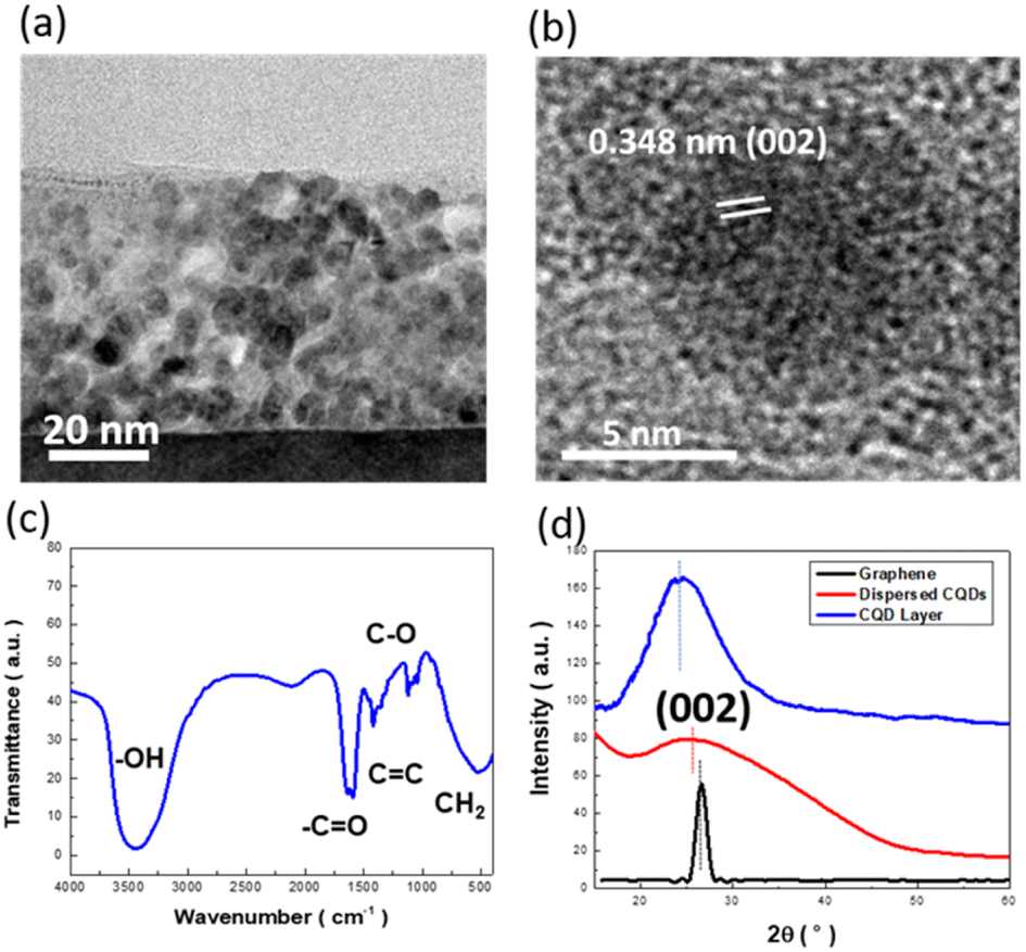 | ||
| Fig. 1 (a) Cross-sectional TEM image of CQDL directly formed on Si substrate. (b) HRTEM image of a representative CQD. (c) FTIR results of CQDL with a thickness of 65 nm. (d) XRD patterns of graphene, dispersed CQDs and CQDL. | ||
Explorations of thickness control over CQDL preparation are displayed in Fig. 2(a). Our findings disclose the reliability of tuning the CQDL thickness by adjusting the cycles of drop coating, where the linear regression of CQDL thickness with respect to the cycling depositions with R2 of 0.998 could be observed. These characteristics displayed sound control over CQDL thickness for the optimization of photodetection capabilities. Another striking property of the CQDL synthesis correlated with consistent film crystallinity by varying the CQDL thickness, as shown in Fig. 2(b). Raman peaks located at 1425 and 1581 cm−1 could be observed, corresponding to the D band and G band of the carbon structures,21–24 respectively, whereas approximately similar intensity ratios, in terms of ID/IG, with a value of 0.66 were in evidence, regardless of a CQDL thickness ranging from 10 to 100 nm. These results indicated sound reliability for further engineering CQDLs in their practical employment in functional optoelectronic applications.
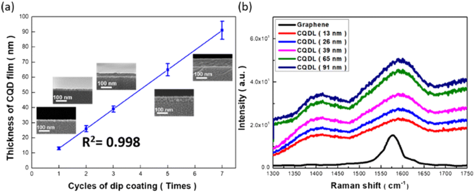 | ||
| Fig. 2 (a) Correlation of CQDL thickness with respect to the cycles of drop coating. (b) Raman results of CQDL with variations in layer thickness. | ||
On the basis of the microstructural, chemical and crystallographic information attained from detailed material characterizations, we attempted to provide insights into the possible mechanism for CQDL formation via in situ self-assembled deposition, where the correlated schematic illustrations are presented in the ESI.† When the drop of CQDs was in contact with Si substrates, a convex surface of the CQD suspension facing Si was formed, which brought about the faster evaporation of the water solvent at the edge of the liquid drop than in the center. This induced a radial outward convective flow from the center along with CQDs to compensate for the partial loss of water solvent due to instant evaporation at the periphery. Moreover, two types of capillary force were created by the deformation of the liquid/air interfaces facing in opposite directions, hydrostatic pressure and surface tension, that were exerted on CQDs at the boundary of the Si substrate and tended to push the self-assembly layered formation of CQDs. While residual water continued to evaporate, the balance of forces was broken, leading to a black surrounding ring formed from an aggregation of CQD clusters at the edge of the substrate surface. This phenomenon has also been observed and interpreted from another two-dimensional ordering of polystyrene sphere nanoparticles by N. Denkov et al.25 Afterwards, a concave meniscus surface of the water solvent forced the CQDs to spread out toward the center of the Si surface. It should be noted that another capillary force, termed sucking capillary pressure, was taking place due to the inherently high hydrophilicity, which mediated the radial inward capillary flux that drove the movement of CQDs toward the unoccupied regions, whereas the involvement of capillary attraction captured the dispersed CQDs towards the ordered region of CQDs.26,27 With such layered formation of CQDs and liquid level drawdown approximately toward the diameter of the CQDs, the hydrostatic pressure and surface tension force were exerted again and applied to an inward convective flow, leading to the multilayered film formation constituted by CQDs.
The spectral light-reflection characteristics of CQDLs with various thicknesses are displayed in Fig. 3(a). To clarify the underlying light/matter interaction, FDTD examinations on light reflectivity were also performed, as shown in Fig. 3(b). It was explicitly found that the experimental results corresponded well with the calculated spectra for bare Si, graphene/Si and five different CQDL/Si. Specifically, the measured average light reflectivity (Rav) of CQDL/Si was found to be fairly low for CQDL thicknesses of 13 nm (Rav = 28.0%) and 26 nm (Rav = 23.8%), where the substantial suppression of light reflectivity was validated compared with either bare Si (Rav = 40.1%) or graphene/Si (Rav = 36.0%) structures, indicating the extraordinary light trapping and utilization capabilities of CQDLs. In addition, the correlated Rav could be further reduced to 17.7%, 16.2% and 13.2% in the cases of 39 nm, 65 nm and 91 nm in CQDL thickness, respectively. All these results essentially reveal the broadband light capture/utilization of CQDLs employed in broadband photosensing applications. To elucidate these findings, the electric-field distributions of CQDL (thickness 65 nm)/Si were calculated under three different light illuminations, of 352 nm, 580 nm and 850 nm, as demonstrated in Fig. 3(c). It could be speculated that the spatial distributions of light trapping effects induced by CQDLs depended on the illumination wavelengths. In general, under short-wavelength (352 nm) illumination, the excited electric fields were substantially confined in the top portions of the CQDLs within the upper two layers of CQDLs owing to the low penetration depth of the incident light. In addition, the regions for field localization of CQDLs extended spatially from the top to the middle range (approximately 1–3 stacked layers and mainly in the 2nd and 3rd stacked layers) and from the top to the bottom range (approximately 1–5 stacked layers and mainly in the 4th and 5th stacked layers) of CQDLs under 580 nm and 850 nm light illumination, respectively. These results explained that the broadband light capturing effects indeed arose through the spectral superposition of light-absorption bands due to the establishment of layered CQD structures rather than the light-induced direct interband transition of individual CQDs, which provided sound evidence for the reflection measurements shown in Fig. 3(a).
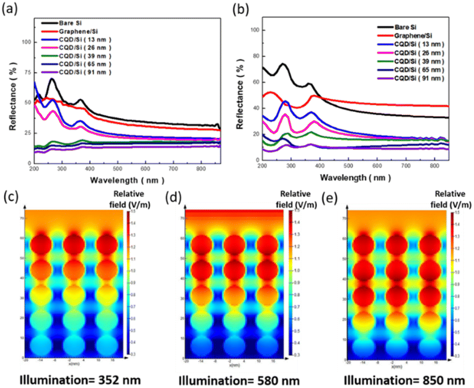 | ||
| Fig. 3 (a) Measured and (b) simulated light-reflection spectra of various samples. FDTD examinations of electric-field distributions of CQDLs (65 nm in thickness) under three various light illuminations: (c) 352 nm, (d) 580 nm and (e) 850 nm. | ||
Photodetection performance
By simply integration with electrode pairs as Ag/CQD/Si/Al sandwiched structures, the CQDL-based photodetectors were created without any sophisticated surface treatment or introducing any additional photonic/collection components. The correlated dark current (I)–voltage (V) relationships of various CQDL-based devices were examined, as shown in Fig. 4(a), and the evaluations of dark currents, and ratio of reverse saturation current and forward/reverse current without the employment of an external bias are summarized in the ESI.† In addition, the dark I–V results of graphene/Si-based devices were also compared. We found that the graphene/Si samples possessed the largest existing dark current (6.02 × 10⁻⁷ A) and reverse saturation current (6.67 × 10⁻³ A), which were an order of magnitude larger in both dark and reversed saturation currents than the correlated results of all CQDL/Si devices. These features could be attributed to the high carrier concentration and large charge mobility inherently existing in the highly conductive graphene layer, which thus inevitably contribute to the service leakage currents that could significantly degrade the photodetection performance.28 By further comparing the device performances of CQDL/Si under dark conditions, the forward/reverse current ratios, functioning as an evaluation of the rectifying behaviors of heterojunction contacts, and depending distinctly on CQDL thickness, are displayed in detail in the ESI.† Specifically, the results indicated that with a CQDL thickness of 13 nm, the corresponding ratio for forward/reverse current reached 527, where the findings closely corresponded to those in the reported literature.29 Nevertheless, the optimal rectifying condition from CQDL/Si photodetectors was achieved when the CQDL thickness increased to 65 nm, reaching a superior ratio of 2.96 × 10⁴, and then gradually decreased to 1.58 × 10⁴ when the CQDL thickness was 91 nm. These features visualized the possible charge blocking phenomena arising from the vertical stacking of CQDs that could facilitate the inhibition of leakage formation reaching the electrode sides. Another possible mechanism that could assist leakage inhibition came from the screening effect from layered CQDLs, because similar charge concentrations appeared in different layered CQDLs and thus could not induce the movement of carriers crossing over the interlayers due to the alleviated driving forces under dark conditions.30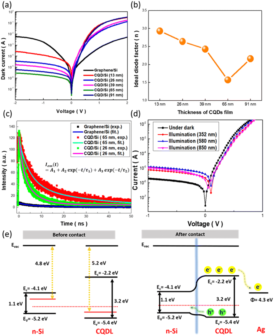 | ||
| Fig. 4 (a) Dark I–V curves of various CQDL/Si and graphene/Si-based devices. (b) Extracted ideal diode factor with respect to the thickness of the CQDL. (c) TRPL examinations of graphene/Si, CQDL (26 nm)/Si and CQDL (65 nm)/Si. The correlated exponential fittings are also shown. (d) Light-driven I–V results of CQDL (65 nm)/Si under various light illuminations. (e) Schematic presentation of band diagrams before and after CQDLs coming into contact with Si substrates. | ||
Another striking piece of evidence regarding the diode behavior of the CQDL/Si heterojunction could be understood through examination of the ideality diode factor, presented as follows,31–33
n = qdV/KTd![[thin space (1/6-em)]](https://www.rsc.org/images/entities/char_2009.gif) lnI lnI | (1) |
In addition, the measured results of time-resolved PL traces at room temperature for the emission peak are displayed in Fig. 4(c). Based on the spectral deconvolution with respect to the PL response, a double exponential equation, I = Aexp(−τ1) + Bexp(−τ2) + C, was utilized for the fitting.34,35 Accordingly, τ1 (τ2) were extracted as 4.95 ns (8.8 ns), 4.77 ns (28.8 ns) and 4.86 ns (16.7 ns) from graphene/Si, CQDL (65 nm)/Si and CQDL (26 nm)/Si, respectively, which were regarded as nonradiative and radiative lifetimes, respectively. A remarkable improvement in radiative carrier lifetime in the case of CQDL (65 nm)/Si could be observed, validating the sound heterojunction involved in the efficient separation of photogenerated carriers that prevented direct charge recombination. In addition, the correlated band diagram is shown in Fig. 4(e), while experimental examinations of the band diagram are demonstrated in the ESI.† When the CQDL was in contact with an n-type Si substrate, interfacial band bending was caused to balance the Fermi-level difference in both sides. Specifically, the edge of the valence band in the CQDL bent upward, which energetically favored the driving of photogenerated holes across interfaces to reach the Si side, which benefited charge separation and in turn avoided direct recombination. On the other hand, a large deviation (2.1 eV) of the conduction band minimum in the CQDL and the work function of the Ag electrode was encountered compared with the energy difference between the conduction band edges of Si and CQDL, termed ΔEc = 1.9 eV. Such circumstances involve a larger rate constant for electron transfer from the CQDL toward the Ag electrode, thus preferentially driving the movement of photogenerated electrons for the generation of photocurrents. Notice that the large potential difference involved could even attain photocurrent formation even when no external bias was employed, and therefore the CQDL/Si could potentially be operated via a self-powered configuration.36,37 These features were evidenced in the measurements of I–V curves under various light illuminations, as shown in Fig. 4(d). Compared with I–V phenomena under dark conditions, remarkably enhanced photoexcited currents covering all the sweeping voltages from −1 to 1 V appeared under the detection of a broad band of light, including 352, 580 and 850 nm.
To evaluate the response time under broadband illumination, repetitive on/off cycles were also recorded, as demonstrated in Fig. 5(a)–(c). Specifically, both the rise time and decay time, defined as the time required for the response to rise from 10% to 90% of the on/off switch peak, and the time required for the response to decay from 90% to 10% of the switch peak, respectively. Accordingly, the evaluated rise time/decay time of devices under 580 nm illumination [Fig. 5(b)] were 12 μs/22 μs, whereas both time parameters turned out to be shorter [6 μs/12 μs, Fig. 5(a)] and longer [14 μs/25 μs, Fig. 5(c)] under 365 nm and 850 nm illumination, respectively. It has been reported that a shorter rise time in terms of switching response correlates with effective photoexcitation and shortened transport length of carriers, and a longer decay time is strongly associated with a reduced probability of carrier recombination, which could be facilitated by charge separation arising from the existence of a heterojunction.
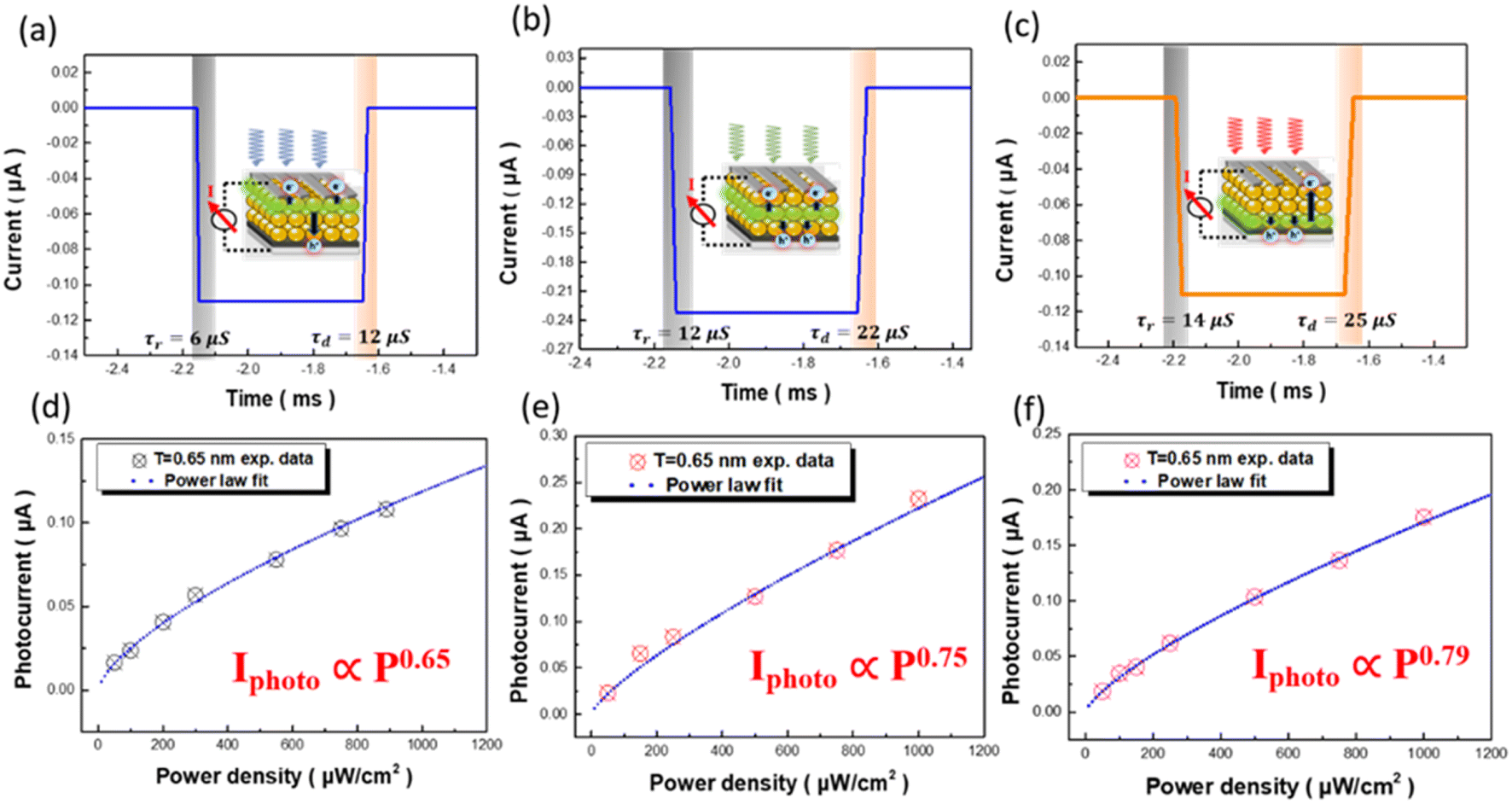 | ||
| Fig. 5 On/off switching of photoresponse for CQDL (65 nm in thickness)/Si photodetectors under light illumination with wavelengths of (a) 365 nm, (b) 580 nm and (c) 850 nm. Relationship between power density of illuminated light with respect to the excitations of photocurrents under illumination wavelengths of (d) 365 nm, (e) 580 nm and (f) 850 nm. | ||
Therefore, we speculated that the distinct dynamic photoexcitation processes of CQDLs depending on illumination wavelengths could be interpreted with the schematic illustrations shown in the insets to Fig. 5(a)–(c), respectively. Under short wavelengths [Fig. 5(a)], the active region for light-absorption/photoexcitation lay in the upper region of the CQDL (highlighted in green) on the basis of FDTD examinations [Fig. 4(c)], and therefore the involvement of rising photocurrent was rapid and responded to the fairly short rise time (6 μs); in contrast, the diminished charge separation, owing to the fact that the existing active CQDL region was far away from the CQDL/Si heterojunction, increased the charge recombination within the CQDL which was in turn reflected in the comparably short decay time. These features could be further supported by the TRPL explorations on thinner CQDL (26 nm)/Si samples, where the reduced radiative carrier lifetime compared with the result of a 65 nm thick CQDL coupled with Si was in evidence, as shown in Fig. 4(c). On the other hand, under long wavelength [Fig. 5(c)], the relatively long transport length for photogenerated electrons to reach the upper electrode and effective hole separation toward the Si side were due to the fact that the active CQDL region for long-wavelength light trapping lay in the proximity of CQDL/Si interfaces. These caused the results of a relatively long rise time and decay time, respectively, in such a spectral situation. Aside from these two spectrally operating edges, one could observe the balance of photoelectron collection and hole separation coming from light illumination with a wavelength of 580 nm, which thus resulted in intermediate rise/decay dynamics compared with short- and long-wavelength excitation. In addition, we also found that the device responsivity (R) and detectivity (D) for sensing 580 nm light reached the highest values among three tested spectral ranges, as detailed in the ESI.† Yet, all the device performances in terms of R and D remained remarkably sound for employment in broadband photodetection applications.
To explore the detection capabilities according to the power intensity of the incident light, the measured photocurrents at zero bias with respect to light power ranging from 0 to 1400 mW cm−2 were examined under three different light illuminations, as shown in Fig. 5(d)–(f), respectively. Mathematical fitting, in terms of power law, was employed to elucidate the underlying power-dependent photosensing characteristics, as presented below,38,39
| Iphoto ∝ Pr | (2) |
Device reliability
Finally, the environmental reliability of the photodetectors was examined, as shown in Fig. 6. Long-term operational tests were performed by conducting 2000 on/off cycles, as shown in Fig. 6(a). The consistent on/off switching without the creation of photocurrent hysteresis within each switch again confirmed the instant signal creation/recovery responding to the spectral variations of the detected light. Aside from that, two practical device parameters, the normalized photocurrent to dark current ratio (NPDR) and noise equivalent power (NEP), were estimated, which clearly validated the maintenance of device reliability for broadband detection, as shown in the ESI.† The influence of environmental temperature on CQDL/Si-based devices was explored by monitoring the device responsivity under a wide temperature range from 0 °C to 400 °C, as shown in Fig. 6(b). It seemed quite promising that the photodetectors could sustain abrupt temperature variations while maintaining a highly stable photosensing response with a slight deviation of less than 1%. These findings indicated the involvement of a quenching effect for the thermal activation of QD architectures, which caused phonon scattering at interparticle edges and thus tended to initiate the non-radiative decay of thermally excited charges that readily diminished the external thermal influences.41Fig. 6(c) presents examinations of the photodetectors under abrasion, where the CQDL/Si devices were subjected to various weight loadings from 0 to 200 g and the CQDL sides were directly polished on a piece of PET film for a length of 50 cm, respectively. The device responsivity recorded with respect to the employment of loading weight explicitly suggested reliable photodetection performances with a trivial reduction in responsivity values of less than 2%, which could be attributed to structural robustness arising from densely layered QD films and approximately defect-free CQDL/Si interfaces. Overall, the results clearly validated the environmental reliability and wearing capability of the devices for potential use in harsh conditions. To shed light on the improvement in device performance, two critical photodetection parameters, the rise time and R of solely nanostructure-based self-powered photodetectors were compared, as shown in Fig. 7, and the detailed results are summarized in the ESI.† The remarkable improvement in device R (9.4 mA W−1) among all the comparative self-powered devices is evident. In addition, the present rise time of CQDL photodetectors in the order of 10−5 s also fell at the top level compared with those in the reported literature. Thus, we would point out that the CQDL/Si self-powered photodetectors could provide excellent sensing responsivity and promising rapid photoresponse dynamics, which might have quite a potential impact on the advanced development of ultrahigh-speed optical communications and further broaden the use of photosensing applications.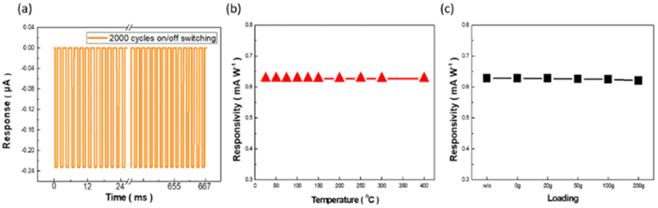 | ||
| Fig. 6 (a) Long-term on/off switching performances of CQDL (65 nm in thickness)/Si photodetectors. Device responsivity of CQDL (65 nm in thickness)/Si photodetectors by examining the influence of (b) environmental temperature and (c) normal loadings on CQDL sides. | ||
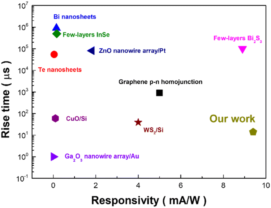 | ||
| Fig. 7 Comparison of device performance of broadband photodetectors in terms of rise time and specific responsivity. | ||
Conclusions
Novel self-powered photodetectors based on thickness-tunable CQDLs were readily manufactured via facile solution deposition. By performing detailed examinations of carrier kinetics, band structures, power-dependent photoresponse characteristics and operational reliability, we found that the CQDL/Si could manifest remarkable photoresponsivity above 9.4 mA W−1 and detectivity above 5.9 × 10¹², and exhibited extremely rapid response with rise time/decay time of <14 μs/<25 μs under broadband light illumination. The superior photodetection performances could be attributed to the synergistic contributions from spatial trapping effects within CQDLs and the established heterojunction that facilitated charge separation, which involved a larger rate constant for electron transfer from a CQDL toward an Ag electrode, thus driving photocurrent generation without the employment of an external bias. Thus, this work could have an impact on the development of single-layer-based photodetectors, and provide further inspiration for other functional photodetection applications.Conflicts of interest
There are no conflicts of interest to declare.Acknowledgements
This work was supported by Ministry of Science and Technology of Taiwan (MOST 110-2223-E-006-003-MY3), and Hierarchical Green-Energy Materials (Hi-GEM) Research Center, from The Featured Areas Research Center Program within the framework of the Higher Education Sprout Project by the Ministry of Education (MOE) and the Ministry of Science and Technology (MOST 107-3017-F-006-003) in Taiwan. The authors greatly thank the Core Facility Center, National Cheng Kung University with the facilities provided for conducting material characterizations.Notes and references
- L. Dou, Y. M. Yang, J. You, Z. Hong, W.-H. Chang, G. Li and Y. Yang, Solution-processed hybrid perovskite photodetectors with high detectivity, Nat. Commun., 2014, 5, 1–6 CrossRef PubMed.
- Z. Zhong, L. Bu, P. Zhu, T. Xiao, B. Fan, L. Ying, G. Lu, G. Yu, F. Huang and Y. Cao, Dark current reduction strategy via a layer-by-layer solution process for a high-performance all-polymer photodetector, ACS Appl. Mater. Interfaces, 2019, 11, 8350–8356 CrossRef CAS PubMed.
- G. Konstantatos, I. Howard, A. Fischer, S. Hoogland, J. Clifford, E. Klem, L. Levina and E. H. Sargent, Ultrasensitive solution-cast quantum dot photodetectors, Nature, 2006, 442, 180–183 CrossRef CAS PubMed.
- T. M. H. Nguyen, S. Kim and C. W. Bark, Solution-processed and self-powered photodetector in vertical architecture using mixed-halide perovskite for highly sensitive UVC detection, J. Mater. Chem. A, 2021, 9, 1269–1276 RSC.
- P. Li, Q. Hao, J. Liu, D. Qi, H. Gan, J. Zhu, F. Liu, Z. Zheng and W. Zhang, Flexible Photodetectors Based on All-Solution-Processed Cu Electrodes and InSe Nanoflakes with High Stabilities, Adv. Funct. Mater., 2022, 32, 2108261 CrossRef CAS.
- Y. Rho, K. Lee, L. Wang, C. Ko, Y. Chen, P. Ci, J. Pei, A. Zettl, J. Wu and C. P. Grigoropoulos, A laser-assisted chlorination process for reversible writing of doping patterns in graphene, Nat. Electron., 2022, 5, 505–510 CrossRef CAS.
- J. Kublitski, A. Hofacker, B. K. Boroujeni, J. Benduhn, V. C. Nikolis, C. Kaiser, D. Spoltore, H. Kleemann, A. Fischer and F. Ellinger, Reverse dark current in organic photodetectors and the major role of traps as source of noise, Nat. Commun., 2021, 12, 1–9 CrossRef PubMed.
- Y. Wei, H. Chen, T. Liu, S. Wang, Y. Jiang, Y. Song, J. Zhang, X. Zhang, G. Lu and F. Huang, Self-Powered Organic Photodetectors with High Detectivity for Near Infrared Light Detection Enabled by Dark Current Reduction, Adv. Funct. Mater., 2021, 31, 2106326 CrossRef CAS.
- M. H. Tran, T. Park and J. Hur, Solution-processed ZnO: graphene quantum dot/poly-TPD heterojunction for high-performance UV photodetectors, Appl. Surf. Sci., 2021, 539, 148222 CrossRef.
- Z. Li, Z. Li, C. Zuo and X. Fang, Application of nanostructured TiO2 in UV photodetectors: a review, Adv. Mater., 2022, 2109083 CrossRef CAS PubMed.
- X. Li, M. Zhu, M. Du, Z. Lv, L. Zhang, Y. Li, Y. Yang, T. Yang, X. Li and K. Wang, High detectivity graphene-silicon heterojunction photodetector, Small, 2016, 12, 595–601 CrossRef CAS PubMed.
- S. Gao, Z. Wang, H. Wang, F. Meng, P. Wang, S. Chen, Y. Zeng, J. Zhao, H. Hu and R. Cao, Graphene/MoS2/Graphene Vertical Heterostructure-Based Broadband Photodetector with High Performance, Adv. Mater. Interfaces, 2021, 8, 2001730 CrossRef CAS.
- X. H. Tai, C. W. Lai, T. C. K. Yang, M. R. Johan, K. M. Lee, C.-Y. Chen and J. C. Juan, Highly effective removal of volatile organic pollutants with pn heterojunction photoreduced graphene oxide-TiO2 photocatalyst, J. Environ. Chem. Eng., 2022, 10, 107304 CrossRef CAS.
- K.-Y. Kuo, S.-H. Chen, P.-H. Hsiao, J.-T. Lee and C.-Y. Chen, Day-night active photocatalysts obtained through effective incorporation of Au@CuxS nanoparticles onto ZnO nanowalls, J. Hazard. Mater., 2022, 421, 126674 CrossRef CAS PubMed.
- H. Nie, M. Li, Q. Li, S. Liang, Y. Tan, L. Sheng, W. Shi and S. X.-A. Zhang, Carbon dots with continuously tunable full-color emission and their application in ratiometric pH sensing, Chem. Mater., 2014, 26, 3104–3112 CrossRef CAS.
- X. Guo, C.-F. Wang, Z.-Y. Yu, L. Chen and S. Chen, Facile access to versatile fluorescent carbon dots toward light-emitting diodes, Chem. Commun., 2012, 48, 2692–2694 RSC.
- L. Tang, R. Ji, X. Cao, J. Lin, H. Jiang, X. Li, K. S. Teng, C. M. Luk, S. Zeng and J. Hao, Deep ultraviolet photoluminescence of water-soluble self-passivated graphene quantum dots, ACS Nano, 2012, 6, 5102–5110 CrossRef CAS PubMed.
- L. Wang, Y. Li, Y. Wang, W. Kong, Q. Lu, X. Liu, D. Zhang and L. Qu, Chlorine-doped graphene quantum dots with enhanced anti-and pro-oxidant properties, ACS Appl. Mater. Interfaces, 2019, 11, 21822–21829 CrossRef CAS PubMed.
- L. Tang, R. Ji, X. Li, K. S. Teng and S. P. Lau, Energy-level structure of nitrogen-doped graphene quantum dots, J. Mater. Chem. C, 2013, 1, 4908–4915 RSC.
- C.-Y. Chen, P.-H. Hsiao, T.-C. Wei, T.-C. Chen and C.-H. Tang, Well incorporation of carbon nanodots with silicon nanowire arrays featuring excellent photocatalytic performances, Phys. Chem. Chem. Phys., 2017, 19, 11786–11792 RSC.
- D. Liu, X. Chen, Y. Hu, T. Sun, Z. Song, Y. Zheng, Y. Cao, Z. Cai, M. Cao and L. Peng, Raman enhancement on ultra-clean graphene quantum dots produced by quasi-equilibrium plasma-enhanced chemical vapor deposition, Nat. Commun., 2018, 9, 1–10 CrossRef PubMed.
- G. Rajender, J. Kumar and P. Giri, Interfacial charge transfer in oxygen deficient TiO2-graphene quantum dot hybrid and its influence on the enhanced visible light photocatalysis, Appl. Catal., B, 2018, 224, 960–972 CrossRef CAS.
- S. Thambiraj and R. Shankaran, Green synthesis of highly fluorescent carbon quantum dots from sugarcane bagasse pulp, Appl. Surf. Sci., 2016, 390, 435–443 CrossRef.
- F. Yuan, Z. Wang, X. Li, Y. Li, Z. a. Tan, L. Fan and S. Yang, Bright multicolor bandgap fluorescent carbon quantum dots for electroluminescent light-Emitting diodes, Adv. Mater., 2017, 29, 1604436 CrossRef PubMed.
- N. Denkov, O. Velev, P. Kralchevski, I. Ivanov, H. Yoshimura and K. Nagayama, Mechanism of formation of two-dimensional crystals from latex particles on substrates, Langmuir, 1992, 8, 3183–3190 CrossRef CAS.
- P. A. Kralchevsky and K. Nagayama, Capillary interactions between particles bound to interfaces, liquid films and biomembranes, Adv. Colloid Interface Sci., 2000, 85, 145–192 CrossRef CAS.
- A. K. S. Kumar, Y. Zhang, D. Li and R. G. Compton, A mini-review: how reliable is the drop casting technique?, Electrochem. Commun., 2020, 121, 106867 CrossRef.
- K. Dave and V. G. Gomes, Carbon quantum dot-based composites for energy storage and electrocatalysis: mechanism, applications and future prospects, Nano Energy, 2019, 66, 104093 CrossRef.
- P.-H. Hsiao, Y.-C. Lai and C.-Y. Chen, Dual-sized carbon quantum dots enabling outstanding silicon-based photodetectors, Appl. Surf. Sci., 2021, 542, 148705 CrossRef CAS.
- L. Zhang, A. Sharma, Y. Zhu, Y. Zhang, B. Wang, M. Dong, H. T. Nguyen, Z. Wang, B. Wen and Y. Cao, Efficient and Layer-Dependent Exciton Pumping across Atomically Thin Organic–Inorganic Type-I Heterostructures, Adv. Mater., 2018, 30, 1803986 CrossRef PubMed.
- S. Mahato and J. Puigdollers, Temperature dependent current-voltage characteristics of Au/n-Si Schottky barrier diodes and the effect of transition metal oxides as an interface layer, Phys. B, 2018, 530, 327–335 CrossRef CAS.
- C.-Y. Chen, T.-C. Wei, P.-H. Hsiao and C.-H. Hung, Vanadium oxide as transparent carrier-selective layer in silicon hybrid solar cells promoting photovoltaic performances, ACS Appl. Energy Mater., 2019, 2, 4873–4881 CrossRef CAS.
- I. R. Putra, J.-Y. Li and C.-Y. Chen, 18.78% hierarchical black silicon solar cells achieved with the balance of light-trapping and interfacial contact, Appl. Surf. Sci., 2019, 478, 725–732 CrossRef CAS.
- A. K. Rana, J. T. Park, J. Kim and C.-P. Wong, See-through metal oxide frameworks for transparent photovoltaics and broadband photodetectors, Nano Energy, 2019, 64, 103952 CrossRef CAS.
- Z. Zheng, J. Yao, L. Zhu, W. Jiang, B. Wang, G. Yang and J. Li, Tin dioxide quantum dots coupled with graphene for high-performance bulk-silicon Schottky photodetector, Mater. Horiz., 2018, 5, 727–737 RSC.
- X. Ren, Z. Li, Z. Huang, D. Sang, H. Qiao, X. Qi, J. Li, J. Zhong and H. Zhang, Environmentally robust black phosphorus nanosheets in solution: application for self-powered photodetector, Adv. Funct. Mater., 2017, 27, 1606834 CrossRef.
- Z. Zhang, Q. Liao, Y. Yu, X. Wang and Y. Zhang, Enhanced photoresponse of ZnO nanorods-based self-powered photodetector by piezotronic interface engineering, Nano Energy, 2014, 9, 237–244 CrossRef CAS.
- D.-S. Tsai, K.-K. Liu, D.-H. Lien, M.-L. Tsai, C.-F. Kang, C.-A. Lin, L.-J. Li and J.-H. He, Few-layer MoS2 with high broadband photogain and fast optical switching for use in harsh environments, ACS Nano, 2013, 7, 3905–3911 CrossRef CAS PubMed.
- A. De Sanctis, G. F. Jones, D. J. Wehenkel, F. Bezares, F. H. Koppens, M. F. Craciun and S. Russo, Extraordinary linear dynamic range in laser-defined functionalized graphene photodetectors, Sci. Adv., 2017, 3, e1602617 CrossRef PubMed.
- A. A. Hussain and A. R. Pal, Enhanced light harvesting through Förster resonance energy transfer in polymer–small molecule ternary system, J. Mater. Chem. C, 2017, 5, 1136–1148 RSC.
- S. Savchenko, A. Vokhmintsev and I. Weinstein, Activation energy distribution in thermal quenching of exciton and defect-related photoluminescence of InP/ZnS quantum dots, J. Lumin., 2022, 242, 118550 CrossRef CAS.
Footnote |
| † Electronic supplementary information (ESI) available. See DOI: https://doi.org/10.1039/d2na00852a |
| This journal is © The Royal Society of Chemistry 2023 |