
 Open Access Article
 This Open Access Article is licensed under a Creative Commons Attribution-Non Commercial 3.0 Unported Licence
Self-array of one-dimensional GaN nanorods using the electric field on dielectrophoresis for the photonic emitters of display pixel†
Sohyeon
Kim
 a,
Hannah
Lee
a,
Gyeong-Hun
Jung
a,
Minji
Kim
a,
Ilsoo
Kim
b,
Myungsoo
Han
b,
Suhan
Lee
c,
Semi
Oh
d,
Jae-Hong
Lim
e and
Kyoung-Kook
Kim
*a
a,
Hannah
Lee
a,
Gyeong-Hun
Jung
a,
Minji
Kim
a,
Ilsoo
Kim
b,
Myungsoo
Han
b,
Suhan
Lee
c,
Semi
Oh
d,
Jae-Hong
Lim
e and
Kyoung-Kook
Kim
*a
aDepartment of IT Semiconductor Convergence Engineering, Research Institute of Advanced Convergence Technology, Tech University of Korea, Siheung 15073, Republic of Korea. E-mail: kim.kk@tukorea.ac.kr
bLG Display Research and Development Center, Seoul 07796, Republic of Korea
cDepartment of Mechanical Engineering, Korea Advanced Institute of Science and Technology (KAIST), Daejeon 34141, Republic of Korea
dGumi Development Research Institute, Gumi Electronics & Information Technology Research Institute (GERI), Gumi 39171, Republic of Korea
eDepartment of Materials Science and Engineering, Gachon University, Seongnam 13120, Republic of Korea
First published on 9th November 2022
Abstract
Recently, high-efficiency III-nitride photonic emitters (PEs) for next-generation displays have been studied. Although micro-light-emitting diodes (μ-LEDs), one of the III-nitride PEs, have attracted considerable attention because of their high efficiency and size flexibility, they have encountered technical limitations such as high defect rate, high processing cost, and low yield. To overcome these drawbacks of μ-LEDs, a lot of research on PEs using one-dimensional (1D) gallium nitride-related nanorods (GNRs) capable of horizontally self-positioning on the electrodes has been carried out. The degree of array of GNRs on the interdigitated electrodes (IDEs) is an important factor in the efficiency of the PEs using GNRs to obtain excellent single-pixel characteristics. Therefore, in this study, we demonstrate that the improved performance of self-arrayed GNRs was realized using the dielectrophoresis technique by changing the thickness of IDEs. In addition, the shape and size of vertically aligned GNRs were controlled by the wet process, and GNR-integrated PEs (GIPEs) were driven by perfectly horizontally self-arrayed GNRs on IDEs. The electroluminescence (EL) intensity of the GIPEs was measured at 4–20 V and showed a maximum intensity value at 15 V. Over the injection voltage at 20 V, the EL intensity decreased due to the high current density of GIPEs. The external quantum efficiency (EQE) property of the GIPEs showed a similar efficiency droop as that of conventional III-nitride PEs.
1. Introduction
In recent decades, III-nitride-related to gallium nitride (GaN)-based photonic emitters (PEs) have been used in general lighting, displays, automobiles, biological agent detection, and sterilization. This is due to their outstanding properties, such as high efficiency and high stability.1–3 Among various applications, the display is one of the industries in high demand for III-nitride PEs. The first use of III-nitride PEs as a display light source was in backlight units (BLUs) of the liquid crystal display (LCD) panel. Recently, there has been increasing research carried out on the miniaturization of PE chips, such as the development of mini light-emitting diodes (mini-LEDs) and micro-light-emitting diodes (μ-LEDs) as a pixel.4,5 μ-LEDs with a chip size of less than 100 μm have attracted significant attention as a light source of pixels for the next-generation displays due to their advantages of high efficiency and size flexibility. Moreover, these μ-LEDs have outstanding properties, such as the realization of excellent image quality and low power consumption compared with the LCDs and the organic light-emitting diodes (OLEDs), both of which are currently the most widely used display light sources in the market.6 However, μ-LEDs encountered a technical limitation in the pick-and-place process to transfer μ-LED chips to the display substrate, which resulted in a high defect rate, high processing cost, low yield, and difficulties in mass production.7,8To overcome these drawbacks of μ-LEDs, considerable research has been conducted on PEs using one-dimensional (1D) GaN-related nanorods (GNRs) capable of horizontal positioning on electrodes.9,10 Particularly, some previous studies have reported that III-nitride PEs using GNRs as single-pixel light sources have significantly higher light efficiency than conventional PEs because of their high crystal quality.11,12 Due to this characteristic, GNR-based PEs can achieve the equivalent single-pixel light output of traditional displays with fewer chips compared to μ-LEDs.
However, to obtain these excellent single-pixel characteristics, the degree of array of GNRs on the electrodes has also emerged as another new technical issue. There are several self-array technologies for 1D nanostructures, such as Langmuir–Blodgett, magnetophoresis, and dielectrophoresis (DEP).13–15 Among them, for GNR self-array, the DEP technology has drawn attention due to its advantage of being able to array numerous GNRs in a wide area with a simple process. In particular, the DEP self-array of GNRs, which have a high aspect ratio (length/diameter) can be conducted at low input voltages.15 DEP uses the property that dipoles induced in an effective electric field (E-field) receive a net force in the direction of a higher E-field density. Here, the effective E-field represents the E-field with an intensity that can force GNRs to self-array between the two sides of the electrodes. Therefore, it is important that the GNRs receive an effective E-field for the formation of stable self-array.
The self-array studies by DEP are influenced by various factors, such as frequency, duration, amplitude of the applied voltage, medium properties, and electrode structure.16–19 Among them, the electrode structure is the key to controlling effective E-field in the device used for PE pixel. Several studies on DEP electrode structures have been reported.19–22 However, previous studies mainly focused on electrode designs and shapes. Moreover, for GNR self-array onto electrodes, there are only a few studies on changing electrode structures. Therefore, we studied the effect of electrode thickness on DEP performance for the realization of self-arrayed GNRs on the electrodes. In addition, we used interdigitated electrodes (IDEs) for DEP electrodes for the fabrication of GNR-integrated photonic emitters (GIPEs) due to their sufficient structural capacity to array high-density GNRs.
In this study, we demonstrated the formation of self-arrayed GNRs by DEP on IDEs and dramatically improved the efficiency of the GIPEs by changing the structure of the IDEs. The shape and diameter of GNRs were controlled by a two-step wet process. Furthermore, the GIPEs were fabricated by horizontally self-arrayed GNRs on IDEs using the effective E-field. The electroluminescence (EL) intensity of the GIPEs was observed at an injection voltage of 4–20 V and showed a maximum value at 15 V. After injection voltage above 20 V, the EL intensity decreased due to the high current density of each GNR in the GIPEs. The external quantum efficiency (EQE) property of the GIPEs showed an efficiency droop similar to that of conventional III-Nitride PEs.
2. Experimental
2.1 GNR fabrication
Fig. 1 shows a schematic of the fabrication procedure of vertically aligned GNRs and GIPEs consisting of horizontally arrayed-GNRs. The III-nitride PE epitaxy wafers were grown via the metal–organic chemical vapor deposition (MOCVD) method. As shown in Fig. 1a, the PE wafers consisted of a 4.7 μm-thick n-GaN, a 50 nm-thick MQWs, a 200 nm-thick p-GaN layer, a 400 nm-thick ITO used as a p-electrode, and a 2 μm-thick SiO2 as a hard mask on the single-polished sapphire substrate. For GNR fabrication, circular-shaped photoresist (PR, AZ GXR-601, AZ Electronic Materials) patterns with a 2 μm spacing were formed by the photo-lithography process on the SiO2 layer, as shown in Fig. 1b. Then, the SiO2 layer was selectively etched using a reactive ion etching (RIE, P-5000, Applied Materials) process. Subsequently, as shown in Fig. 1c, the epitaxy layer was etched by an inductively coupled plasma (ICP, Multiplex ICP, STS) process until the sapphire substrate was exposed. To control the shape and diameter of the GNRs, a wet etching process was performed using a KOH solution (5 mol) at 80 °C, as shown in Fig. 1d–e. Then, a 40 nm-thick Al2O3 layer was deposited on the sidewall of GNRs by atomic layer deposition for passivation, as shown in Fig. 1f. To separate the GNRs from the substrate, as shown in Fig. 1g, the GNR-fabricated wafer was immersed in acetone and ultrasonicated at 400 W for 40 min. Acetone acts as a suspending medium for the separation of GNRs. The length of separated GNRs was confirmed to average 4.7 μm.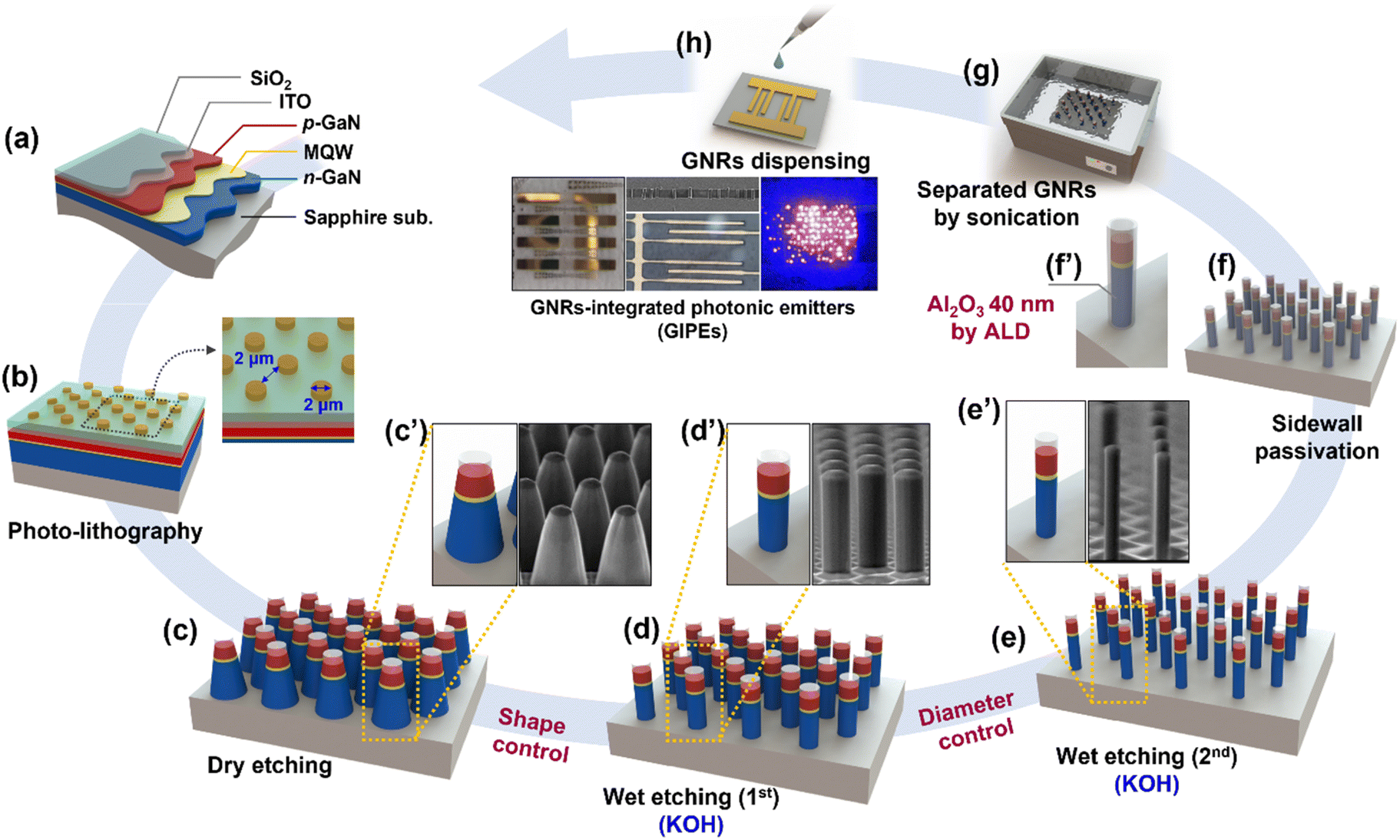 | ||
| Fig. 1 (a) to (f) Schematic illustration of the fabrication procedure for vertically aligned GNRs on the sapphire substrate, (g) GNR separation, and (h) GNRs dispensing on the IDEs for GIPEs. The FE-SEM images of (c′) dry etched GNRs, (d′) first wet etched GNRs, and (e′) second wet etched GNRs. | ||
2.2 IDE fabrication
For the electrode fabrication, a single-polished sapphire was used as the substrate, which was cleaned with acetone, isopropyl alcohol (IPA), and deionized (DI) water. The interdigitated PR patterns were formed on the sapphire substrate. Then, the titanium (Ti) and gold (Au) layers were deposited using an e-beam evaporator. Later, a 50 nm-thick Ti layer was deposited for an adhesive layer. Then, Au was deposited in three thicknesses of 100, 750, and 1550 nm. The Ti/Au layer on the PR pattern was removed by the lift-off process with ultrasonication in acetone. Finally, the three types of Ti/Au IDE structures with different thicknesses of 150, 800, and 1600 nm were obtained. The electrode size was 1.7 × 16.5 mm2 consisting of contact pads and IDE units of 400 ea with 7 μm width and 4 μm spacing (Fig. S3†).2.3 Self-arrayed GNRs
The DEP-assisted GNR self-array process was conducted in a probe station using a function generator (WF 1945A, NF Corp.) and a power amplifier (4005, NF Corp.). The separated GNRs in acetone were dropped with a micro-pipette onto the IDEs, which were connected with probe tips under an AC voltage. The frequency and amplitude of the AC voltage were set at 1 MHz and 4 Vrms, respectively.2.4 GNR characterization
The vertically aligned GNRs on the substrate and the horizontally self-arrayed GNRs on the IDEs were observed by field emission scanning electron microscopy (FE-SEM, S4300, Hitachi). To characterize the optical properties of the GNRs, the light output intensity-injection current (L–I), EQE, and EL were measured using a parameter analyzer (model 2420, Keithley Instruments Inc.) and an optical power meter (model 1830C, Newport Corp.) with a probe station. The emission images were observed using an optical microscope (OM) and a color charge-coupled device (CCD) camera (CVC-5220, Veltek).3. Result and discussion
Fig. 2 shows the FE-SEM images of vertically aligned GNRs after the dry (Fig. 2a) and wet etching process (Fig. 2b and c). The top surface diameter of the tapered GNRs was observed to be approximately 1.5 μm after the dry etching process, as shown in Fig. 2a. To fabricate the tapered GNRs for making columnar shape, the first-step KOH wet etching process was conducted for 90 min. In Fig. 2b, the diameter of the column-shaped GNRs was approximately 1.5 μm, which is the same as the top surface diameter of the tapered GNRs. The FE-SEM image in Fig. 2c shows that GNRs approximately 0.8 μm in diameter were vertically aligned on the substrate after the second-step KOH wet etching process for an additional 30 min.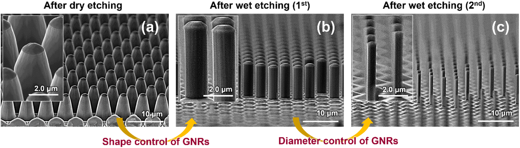 | ||
| Fig. 2 FE-SEM images of (a) the vertically aligned GNRs on the sapphire substrate after dry etching process and (b) and (c) the shape and diameter variation of the GNRs by the two-step KOH wet etching process. | ||
Further, the shape and diameter of GNRs could be controlled by the KOH wet etching time, as shown in Fig. 3. The bottom diameters of GNRs after the wet etching process for 30 and 60 min were 4.15 and 3.57 μm, respectively. These bottom diameters of GNRs were larger than the 2 μm-diameter of the PR mask pattern. In other words, when the KOH wet etching process was performed within 90 min, the shape of GNRs was controlled, and the shape of the GNR sidewalls changed from tapered to columnar. Moreover, in the case of the KOH wet etching process for more than 90 min, the diameters of the column-shaped GNRs decreased with the increase in the wet etching time. The average diameters of GNRs after the KOH wet etching process for 90, 120, 150, and 180 min were 1.48, 0.81, 0.79, and 0.36 μm, respectively. For GIPE fabrication, we obtained the GNRs with a 0.81 μm diameter by 120 min KOH wet etching process.
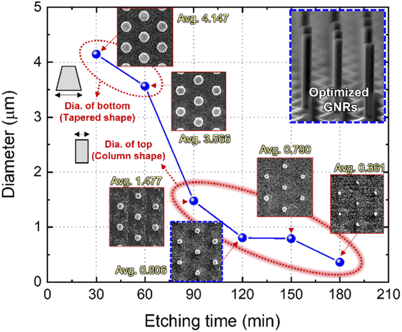 | ||
| Fig. 3 The average diameter of GNRs vs. KOH wet etching time plot with FE-SEM top view images of the vertically aligned GNRs on the sapphire substrate. | ||
Fig. 4 shows the shape control mechanism of the GNRs by selectively etching process of the GNR sidewall using a KOH solution. Fig. 4a shows the atomic-bonding structure of the top (c-plane) and sidewall (r-plane) of the dry-etched atomic structure with the tapered shape of GNRs. In the case of the c-plane, oxygen in the air might be adsorbed with Ga ions on the surface after the dry etching process. When GaN is immersed in KOH solution, the Ga layer with the adsorbed oxygen molecules is removed and the surface turns into N-termination. Hydroxide ions (OH−) cannot approach the surface due to the repulsive force between OH− and the negatively charged N dangling bonds. Then, the reaction is terminated. Moreover, in the case of the r-plane, OH− ions adsorb on the positively charged Ga dangling bonds, as shown in Fig. 4b1. Then, as shown in Fig. 4b2, the OH− ions adsorb all the dangling bonds of Ga ions, and gallium oxide (Ga2O3) and ammonia (NH3) are generated. Finally, Ga2O3 dissolves in an alkali solution, as shown in Fig. 4b3. This reaction can be represented by the following equation:
| 2GaN + 3H2O → Ga2O3 + 2NH3 |
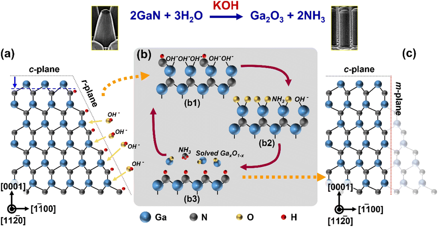 | ||
| Fig. 4 Schematic diagram of the mechanism for changing the shape of vertically aligned GNRs by KOH wet etching process. The atomic structure diagram of (a) a tapered GNR, (b1) adsorbed OH− ions on the GaN surface, (b2) gallium oxide (Ga2O3) and ammonia (NH3) generation, (b3) Ga2O3 dissolution, and (c) a columnar GNR. | ||
Fig. 5a shows three possible positions of a single GNR during the self-array process using DEP. Here, non-arrayed, semi-arrayed, and arrayed GNRs are defined as GNRs not connected to either electrodes, GNRs connected to one of the two electrodes on either side, and GNRs connected to both electrodes, respectively. The degree of the GNR self-array can be affected by the DEP force, as shown in Fig. 5b. For a nanorod suspended in a medium in an AC electric field, the time-averaged DEP force is represented by the following formula:
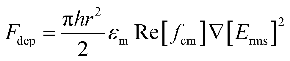
 | ||
| Fig. 5 The illustrated images of (a) dispensed GNRs on the electrodes under AC electric field and (b) to (e) effective E-field area changed by IDE thickness affecting the DEP force. The simulation results of E-field generated between electrodes with ideal structure of thickness (c′) 150 nm, (d′) 800 nm, and (e′) 1600 nm, respectively. FE-SEM images of horizontally positioned GNRs on IDEs of thicknesses (c′′) 150 nm, (d′′) 800 nm, and (e′′) 1600 nm, respectively. | ||
Fig. 5c′′–e′′ show FE-SEM images of the self-arrayed GNRs. In the case of the 150 nm thick-IDEs (where the thickness of the IDEs is less than the diameter of the GNRs), as shown in Fig. 5c′′, the number of arrayed GNRs was seldom. Moreover, non-arrayed and semi-arrayed GNRs were normally observed. Fig. 5d′′ shows GNRs on 800 nm thick-IDEs (where the thickness of the IDEs is the same as the diameter of the GNRs), which are semi-arrayed and arrayed between the electrodes. The number of arrayed GNRs is much higher than that in the 150 nm thick-IDEs. Lastly, in the case of the 1600 nm-thick IDEs (where the thickness of the IDEs is twice the diameter of the GNRs), as shown in Fig. 5e′′, mostly self-arrayed GNRs were observed compared to the GNR arrayed with the both 150 and 800 nm thick-IDEs. Typically, the enhanced degree of self-arrayed GNRs was confirmed with increasing IDE thickness and is similar to the models we assumed in Fig. 5c–e, and the simulation results are displayed in Fig. 5c′–e′.
To evaluate the optical properties of the GNRs, we fabricated GIPEs with the 1600 nm-thick IDEs and measured L–I and EL intensity. Then, the GIPEs were packaged on a printed circuit board (Fig. S4†). Fig. 6a shows the light output power (LOP) and EQE under the current injection. The LOP of the GIPEs increased almost linearly with the applied current. The EQE result showed a decrease from 2.6% to 0.8% at 0.005 mA and 0.06 mA, respectively. The EQE value was lower compared to the EQE value of the other reports.10 However, the measurement results of the GIPE fabricated in this study could not be directly compared with other literature because the important parameters for measurement, such as the chip size, number of GNRs, and process conditions, are all different (Table S1†). Moreover, only a few studies related to PEs using horizontally self-arrayed GNRs have been reported to date.
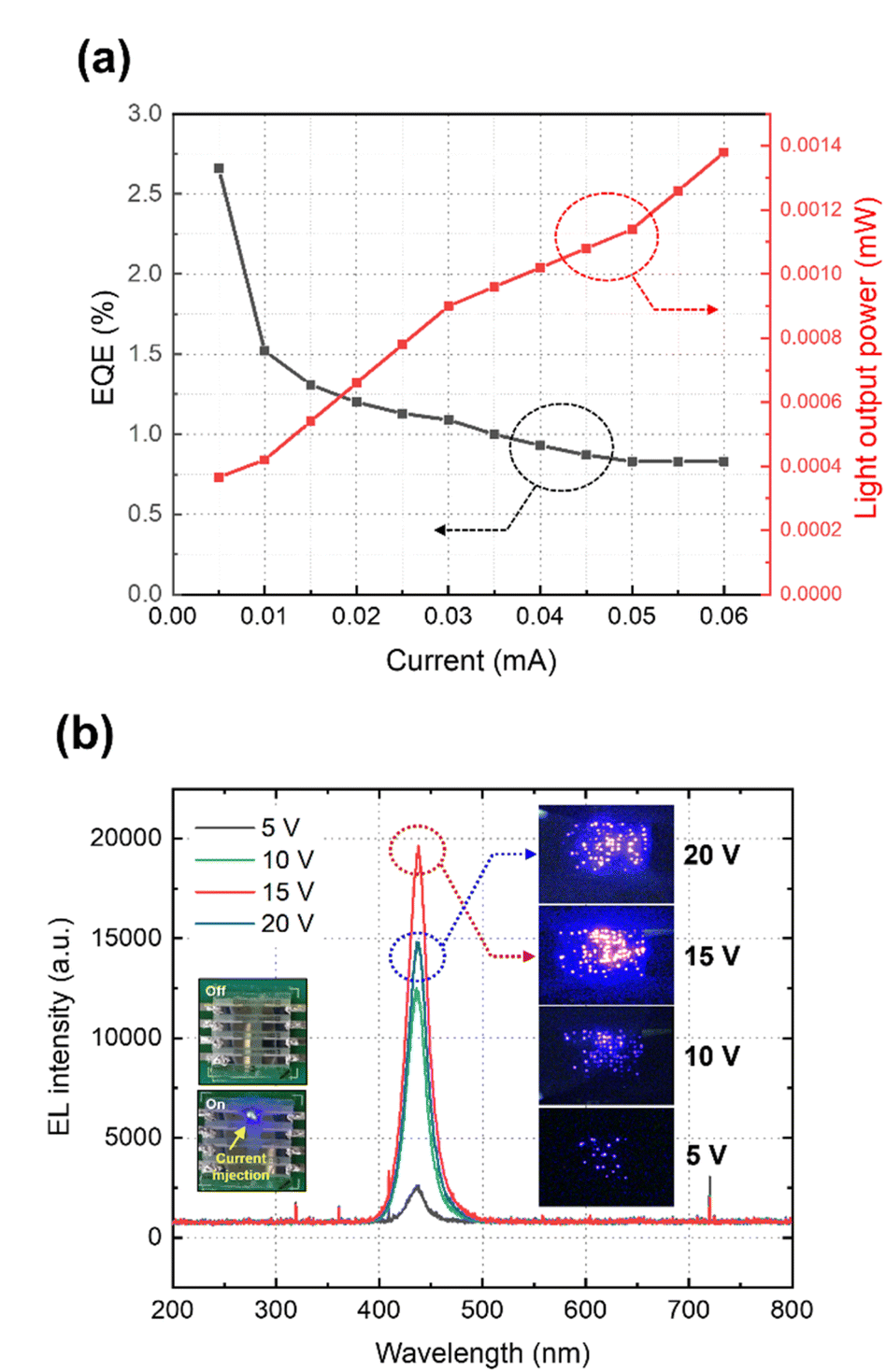 | ||
| Fig. 6 (a) L–I curve and EQE result vs. injection current, (b) EL intensity and emission images of the GIPEs consisting of horizontally self-arrayed GNRs on IDEs. | ||
This EQE droop has mainly three causes:
(1) First, it is because the current density of a single GNR, which is the current per unit area, increases as the applied current increases. As a single GNR has a small emission area, it has more current density even if the same current is injected compared to conventional III-nitride PEs (Fig. S1†). Therefore, GNRs are converted to a non-radiative channel when high current is applied. This phenomenon of low efficiency at high current density is a general characteristic of conventional III-nitride PEs.24,27
(2) Second, large amounts of heat are generated in GIPEs because a GNR has a high current density, as mentioned earlier. A portion of the injected current is converted into heat, which degrades the performance of GIPEs. Conventional III-nitride PEs show good thermal conduction properties, as it is in bulk states, and heat is released to the electrode or the substrate. However, GIPEs designed on a sapphire substrate have low thermal conductivity and poor heat dissipation properties.
(3) Finally, it is because of the poor photon collection of GIPEs during the EQE measurement. Photon extraction efficiency (PEE) affects the EQE of III-nitride PEs, as shown in the following equation:
| EQE = IQE × PEE |
Fig. 6b shows the EL peak wavelengths at the injection voltage of 5, 10, 15, and 20 V. The EL peaks tend to be red-shifted as the applied voltage increases, which is a common characteristic of PEs, that occurs due to a lot of heat generated when a lot of current flows. The EL intensity of the GIPEs was observed starting at 4 V and increased as the applied voltage increased to 15 V. The GIPEs were stable when driven from 4 V to 15 V with sustained time periods. Above 20 V, the EL intensity was higher than that at 15 V just after voltage application (Fig. S2†). However, after 10–20 s, the EL intensity significantly decreased by 25% compared to that at 15 V because of the high current density of GNRs in the GIPEs. The reason for the high operating voltages was because of the high ohmic contact resistance. There was no additional contact layer between the GNRs and IDEs for electrical connection. To reduce the ohmic contact resistance, additional top IDEs, which buried the ends of the GNRs as a sandwich structure, will be needed with bottom IDEs (Fig. S5†). The inset images on the left side of Fig. 6b show the packaged GIPEs and their emission under the current injection. The inset images on the right side of Fig. 6b are the OM images of the GIPE emission under applied voltages of 5–20 V. It is confirmed that the emission at 15 V was the brightest, which is consistent with the trend of the EL intensity. In addition, the EL emissions of the GIPEs with 150 nm-thick IDEs and 800 nm-thick IDEs at 15 V were weaker than that of the GIPE with 1600 nm-thick IDEs (Fig. S6†).
4. Conclusions
In conclusion, we fabricated GIPEs with horizontally self-arrayed GNRs on IDEs for the next-generation displays. The shape and diameter of the vertically aligned GNRs on the sapphire substrate were perfectly controlled by the two-step KOH wet etching process. The sidewall shape of GNRs changed from tapered to columnar shapes by the wet etching process performed for 90 min. Prolonged etching for more than 90 min decreased the diameters of the columnar GNRs. Then, the separated GNRs were self-arrayed on IDEs, with thicknesses of 150, 800, and 1600 nm, by the DEP technology.To improve the self-arrayed GNR properties, we demonstrated that the self-array performance was enhanced by the effective E-field area, which increased with the IDE thickness. The EQE of the GNRs on 1600 nm-thick IDEs showed a decrease from 2.6% to 0.8% at 0.005 mA and 0.06 mA, respectively. Moreover, the EL intensity decreased under a high-voltage application. This was due to poor heat dissipation, poor photon collection, and high current density problems. The fabricated GIPEs had no bottom reflective layer and no structures for photon extraction. In addition, there was no additional contact layer between the GNRs and IDEs. Therefore, to fabricate pixel emitters of the GNR-based display, a higher EQE is expected to be obtained if heat dissipation structures, reflective layers, and connecting metal layers between GNRs and IDEs are added to the GIPEs in future works.
Author contributions
S. Kim, I. Kim, M. Han, and K.-K. Kim conceived and designed the experiments; S. Kim and H. Lee conducted investigation; S. Kim, H. Lee, G.-H. Jung, M. Kim, and S. Lee performed the experiments and formal analysis; S. Kim, H. Lee, and K.-K. Kim analysed the data; J.-H. Lim conducted the simulation; S. Kim wrote the manuscript; S. Oh and K.-K. Kim performed review and editing; I. Kim and M. Han initiated and funded the project; K.-K. Kim contributed to supervision. All authors contributed to discussion of the results and agreed to the published version of the manuscript.Conflicts of interest
There are no conflicts to declare.Acknowledgements
This research was funded by LG Display, Korea Institute for Advancement of Technology (KIAT) grant funded by the Korea Government (MOTIE) (P0008458, HRD Program for Industrial Innovation), and the MSIT (Ministry of Science and ICT), Korea, under the ITRC (Information Technology Research Center) support program (IITP-2018-0-01426) supervised by the IITP (Institute for Information & Communications Technology Planning & Evaluation).Notes and references
- H. S. Wasisto, J. D. Prades, J. Gulink and A. Waag, Appl. Phys. Rev., 2019, 6, 041315 Search PubMed.
- W.-S. Lee, S.-H. Kwon, H.-J. Choi, K.-G. Im, H. Lee, S. Oh and K.-K. Kim, Micromachines, 2020, 11, 346 CrossRef PubMed.
- S.-J. Kim, S. Oh, K.-J. Lee, S. Kim and K.-K. Kim, Micromachines, 2021, 12, 399 CrossRef PubMed.
- T. Wu, C.-W. Sher, Y. Lin, C.-F. Lee, S. Liang, Y. Lu, S.-W. H. Chen, W. Guo, H.-C. Kuo and Z. Chen, Appl. Sci., 2018, 8, 1557 CrossRef.
- Y. Huang, E.-L. Hsiang, M.-Y. Deng and S.-T. Wu, Light: Sci. Appl., 2020, 9, 105 CrossRef CAS PubMed.
- Z. Wang, X. Shan, X. Cui and P. Tian, J. Semicond., 2020, 41, 041606 CrossRef CAS.
- Y.-M. Huang, J.-H. Chen, Y.-H. Liou, K. J. Singh, W.-C. Tsai, J. Han, C.-J. Lin, T.-S. Kao, C.-C. Lin, S.-C. Chen and H.-C. Kuo, Nanomaterials, 2021, 11, 2696 CrossRef CAS PubMed.
- Z. Chen, S. Yan and C. Danesh, J. Phys. D: Appl. Phys., 2021, 54, 123001 CrossRef CAS.
- H. K. Park, S. W. Yoon, Y. J. Eo, W. W. Chung, G. Y. Yoo, J. H. Oh, K. N. Lee, W. Kim and Y. R. Do, Sci. Rep., 2016, 6, 28312 CrossRef CAS PubMed.
- M. Sheen, Y. Ko, D.-U. Kim, J. Kim, J.-H. Byun, Y. Choi, J. Ha, K. Y. Yeon, D. Kim, J. Jung, J. Choi, R. Kim, J. Yoo, I. Kim, C. Joo, N. Hong, J. Lee, S. H. Jeon, S. H. Oh, J. Lee, N. Ahn and C. Lee, Nature, 2022, 608, 56 CrossRef CAS PubMed.
- Y.-H. Ra, R. Wang, S. Y. Woo, M. Djavid, S. M. Sadaf, J. Lee, G. A. Botton and Z. Mi, Nano Lett., 2016, 16, 4608 CrossRef CAS PubMed.
- Q. Li, K. R. Westlake, M. H. Crawford, S. R. Lee, D. D. Koleske, J. J. Figiel, K. C. Cross, S. Fathololoumi, Z. Mi and G. T. Wang, Opt. Express, 2011, 19, 25528 CrossRef CAS PubMed.
- F. Kim, S. Kwan, J. Akana and P. Yang, J. Am. Chem. Soc., 2001, 123, 4360 CrossRef CAS PubMed.
- P. Moritz, 2020 IEEE 33rd International Conference on Micro Electro Mechanical Systems (MEMS), Vancouver, BC, Canada, January, 2020 Search PubMed.
- Y. J. Eo, G. Y. Yoo, H. Kang, Y. K. Lee, C. S. Kim, J. H. Oh, K. N. Lee, W. Kim and Y. R. Do, ACS Appl. Mater. Interfaces, 2017, 9, 37912 CrossRef CAS PubMed.
- A. K. Naieni and A. Nojeh, Nanotechnology, 2012, 23, 495606 CrossRef PubMed.
- M. Duchamp, K. Lee, B. Dwir, J. W. Seo, E. Kapon, L. Forró and A. Magrez, ACS Nano, 2010, 4, 279 CrossRef CAS PubMed.
- J. Castillo, S. Tanzi, M. Dimaki and W. Svendsen, Electrophoresis, 2008, 29, 5026 CrossRef CAS PubMed.
- H. Zhang, H. Chang and P. Neuzil, Micromachines, 2019, 10, 423 CrossRef PubMed.
- R. Zhou, P. Wang and H.-C. Chang, Electrophoresis, 2006, 27, 1376 CrossRef CAS PubMed.
- R.-Z. Lin, C.-T. Ho, C.-H. Liu and H.-Y. Chang, Biotechnol. J., 2006, 1, 949 CrossRef CAS PubMed.
- Y. Wang, F. Du, M. Baune and J. Thöming, Microfluid. Nanofluid., 2014, 17, 499 CrossRef CAS.
- Y.-Y. Lai, S.-C. Hsu, H.-S. Chang, Y. S. Wu, C.-H. Chen, L.-Y. Chen and Y.-J. Chen, Res. Chem. Intermed., 2017, 43, 3563 CrossRef CAS.
- J. Cho, E. F. Schubert and J. K. Kim, Laser Photonics Rev., 2013, 7, 408 CrossRef CAS.
- S. Zhou, B. Cao, S. Liu and H. Ding, Opt. Laser Technol., 2012, 44, 2302 CrossRef CAS.
- X. Jin, 2015 IEEE 15th International Conference on Nanotechnology (IEEE-NANO), Rome, Italy, July, 2015 Search PubMed.
- P. Tian, J. J. D. McKendry and Z. Gong, Appl. Phys. Lett., 2012, 101, 231110 CrossRef.
Footnote |
| † Electronic supplementary information (ESI) available. See DOI: https://doi.org/10.1039/d2na00496h |
| This journal is © The Royal Society of Chemistry 2023 |