
 Open Access Article
 This Open Access Article is licensed under a Creative Commons Attribution-Non Commercial 3.0 Unported Licence
Impact of coherent core/shell architecture on fast response in InP-based quantum dot photodiodes†
Kazuhiro
Nemoto
 ab,
Junpei
Watanabe
bc,
Hiroyuki
Yamada
ab,
Hong-Tao
Sun
b and
Naoto
Shirahata
*abc
ab,
Junpei
Watanabe
bc,
Hiroyuki
Yamada
ab,
Hong-Tao
Sun
b and
Naoto
Shirahata
*abc
aGraduate School of Chemical Sciences and Engineering, Hokkaido University, Sapporo 060-0814, Japan
bInternational Center for Materials Nanoarchitectonics (MANA), National Institute for Materials Science (NIMS), 1-1 Namiki, Tsukuba 305-0044, Japan. E-mail: SHIRAHATA.Naoto@nims.go.jp
cDepartment of Physics, Chuo University, 1-13-27 Kasuga, Bunkyo, Tokyo 112-8551, Japan
First published on 17th January 2023
Abstract
Solution-processed, cadmium-free quantum dot (QD) photodiodes are compatible with printable optoelectronics and are regarded as a potential candidate for wavelength-selective optical sensing. However, a slow response time resulting from low carrier mobility and a poor dissociation of charge carriers in the optically active layer has hampered the development of the QD photodiodes with nontoxic device constituents. Herein, we report the first InP-based photodiode with a multilayer device architecture, working in photovoltaic mode in photodiode circuits. The photodiode showed the fastest response speed with rising and falling times of τr = 4 ms and τf = 9 ms at a voltage bias of 0 V at room temperature in ambient air among the Cd-free photodiodes. The single-digit millisecond photo responses were realized by efficient transportation of the photogenerated carriers in the optically active layer resulting from coherent InP/ZnS core/shell QD structure, fast separation of electron and hole pairs at the interface between QD and Al-doped ZnO layers, and optimized conditions for uniform deposition of each thin film. The results suggested the versatility of coherent core/shell QDs as a photosensitive layer, whose structures allow various semiconductor combinations without lattice mismatch considerations, towards fast response, high on/off ratios, and spectrally tunable optical sensing.
1. Introduction
Colloidal quantum dots (QDs) have tunable excited states depending on their diameters based on the quantum confinement effect, and their excellent optical absorption and emission properties have attracted attention in a wide range of optoelectronic applications, including photodetectors,1–3 solar cells,4,5 light-emitting diodes,6,7 and lasers.8 QD photodetectors have a device structure of primarily photodiodes or phototransistors and can be manufactured at low cost, offering significant advantages in surveying, night vision, optical communications, thermal sensing, and medical diagnostics.9 To date, the ultraviolet spectral range is covered by the QDs having a central element of ZnO or ZnS,10,11 while counterparts of CsPbBr3 and CdSe have been developed to cover the visible wavelength range.12,13 QDs of PbS, PbSe, and CdSexTe1−x dominate the optically active layers for near-infrared (NIR) light sensing.14–16Group III–V compound semiconductors find various applications in optoelectronics for the reasons below.17–19 First, their high electron mobilities such as 78![[thin space (1/6-em)]](https://www.rsc.org/images/entities/char_2009.gif) 000 cm2 V−1 s−1 for InSb,20 34000 cm2 V−1 s−1 for InAs,21 9400 cm2 V−1 s−1 for GaAs,21 and 5200 cm2 V−1 s−1 for InP21 are beyond the values of other semiconductors including Si (1450 cm2 V−1 s−1),22 CdTe (804 cm2 V−1 s−1),23 CdSe (642 cm2 V−1 s−1),23 and CdS (642 cm2 V−1 s−1).23 Second, some of group III–V compound semiconductors (except for GaN, AlAs, AlSb, GaN, and GaP) have low exciton binding energy,24 making it easier to dissociate excitons and extract a net current from the device flow towards the corresponding electrodes for detection of photons. Third, the absorption and emission spectral tunability in a broad wavelength range is realized by a controlled energy gap resulting from alloying of central elements of QDs or their size control.25,26 Fourth, III–V semiconductors are free of toxic heavy metals such as Cd, Pb, and Hg, making them an attractive alternative material platform for optoelectronic device applications.27,28 Nevertheless, compared to group II–VI semiconductor QDs, III–V counterparts have a higher ratio of covalent bond character against the ionic bond one, making nanoparticle crystallization in the solution phase difficult and leaving challenges in their synthesis.
000 cm2 V−1 s−1 for InSb,20 34000 cm2 V−1 s−1 for InAs,21 9400 cm2 V−1 s−1 for GaAs,21 and 5200 cm2 V−1 s−1 for InP21 are beyond the values of other semiconductors including Si (1450 cm2 V−1 s−1),22 CdTe (804 cm2 V−1 s−1),23 CdSe (642 cm2 V−1 s−1),23 and CdS (642 cm2 V−1 s−1).23 Second, some of group III–V compound semiconductors (except for GaN, AlAs, AlSb, GaN, and GaP) have low exciton binding energy,24 making it easier to dissociate excitons and extract a net current from the device flow towards the corresponding electrodes for detection of photons. Third, the absorption and emission spectral tunability in a broad wavelength range is realized by a controlled energy gap resulting from alloying of central elements of QDs or their size control.25,26 Fourth, III–V semiconductors are free of toxic heavy metals such as Cd, Pb, and Hg, making them an attractive alternative material platform for optoelectronic device applications.27,28 Nevertheless, compared to group II–VI semiconductor QDs, III–V counterparts have a higher ratio of covalent bond character against the ionic bond one, making nanoparticle crystallization in the solution phase difficult and leaving challenges in their synthesis.
InP QDs are the most well-studied nanocrystals among the III–V family, but their application remains limited to the optically active layer of light-emitting diodes.29,30 There are only a few reports of InP QDs applied to photoelectrodes, and until now, only two reports of phototransistor structures.31,32 Kwak and co-workers reported a hybrid phototransistor where InP QDs were used as a light-absorbing layer while black phosphorus (BP) was used as a transportation layer.31 In their study, the ligand exchange from oleylamine to 1,2-ethanedithiol, which has a shorter alkyl length, and annealing at high temperature for InP QDs improved the charge injection of the photogenerated carriers from the QD layer to BP layer, leading to a high responsivity and detectivity, but slow speed with a fall time of 120 ms. The slow response speed for fall time is a common problem of entire Cd-free QD photodetectors not limited to III–V counterparts.1,3,32
Here we report, for the first time, a vertical III–V QD photodiode having a high-speed response of rise time of 4 ms and fall time of 9 ms even at a voltage bias of 0 V at room temperature in ambient air. In this device structure, a coherent InP/ZnS core–shell QD as a light-absorbing layer having a single lattice parameter was used. The lattice coherency allowed for high carrier mobility throughout the core/shell QD resulting from the emerging defect-less core/shell interface. A ligand-exchange strategy was developed, in which palmitic acid on the QD with a shorter ligand, i.e., 6-mercapto-1-hexanol, led to greatly improved quality of the QD film by spin coating. Furthermore, the spatial separation of photogenerated excitons was realized by forming a type-II band alignment at the interface between the QD layer and the Al-doped ZnO counterpart, resulting in a fast response at a single-digit millisecond scale.
2. Experimental
2.1 Reagents and materials
Indium(III) acetate [In(Ac)3, 99.99%, Aldrich], zinc acetate [Zn(Ac)2, 99.99%, Aldrich], zinc oxide (ZnO, 99.999%, Aldrich), 1-octadecene (ODE, 90%, Aldrich), sulfur (99.98%, Aldrich), butylamine (99.5%, Aldrich), N,N-dimethylformamide (DMF, anhydrous, 99.8%, Aldrich) oleic acid (OA, 90%, Aldrich), trioctylphosphine (TOP, 97%, Aldrich), 1-dodecanethiol (DDT, >98%, Aldrich), tris(trimethylsilyl)-phosphine [(TMS)3P, 98% Strem Chemicals], palmitic acid (PA, 98%, Tokyo Chemical Industry), n-octylamine (OAm, 98%, Tokyo Chemical Industry), 6-mercapto-1-hexanol (MCH, 97%, Aldrich), and aluminium-doped zinc oxide ink (conductivity: 10−3–10−4 S cm−1, viscosity < 4 mPa s, Aldrich) were used without further purification. Aluminium (Al) wires were purchased from the Nilaco Corporation (Japan). The purity of argon gas was 99.999%. Using an oil rotary vacuum pump, the vacuum conditions of less than 60 Pa were used for degassing and argon gas purge.2.2 Preparation of Zn-oleate
ZnO (2 mmol) and OA (8 mmol) were mixed with 10 mL ODE in a 50 mL three-necked flask. The temperature was measured using a thermocouple inserted directly into the flask from one branch pipe. The other branch pipe was capped with a silicone rubber septum for injection of stainless-steel syringe needles. The flask was connected to the Schlenk line. At first, the system was purged five times with argon gas. The mixture was degassed at 120 °C for 2 h under vacuum conditions, and then the mixture was quickly heated in an argon flow to 290 °C and kept for about 1 h until the mixed solution got transparent for yielding Zn-oleate. The solution was then cooled down to room temperature and stored in an argon-filled vial until use.2.3 Preparation of (TMS)3P–TOP
(TMS)3P (0.12 mmol) in hexane was dissolved in 1 mL of TOP at room temperature inside an argon-filled glovebox where the oxygen and water levels are continuously monitored to maintain both O2 ≤ 1 ppm and H2O ≤ 5 ppm. The mixture was gently stirred until becoming a uniform solution. This step was performed on the day before the synthesis of InP QD.2.4 Synthesis of InP QDs
0.45 mmol of In(Ac)3, 0.075 mmol of Zn(Ac)2, and PA (0.5 mmol) were mixed with 6.3 mL of ODE in a 50 mL three-necked flask which is fixed to a Schlenk line with a reflux condenser. Degassing of the mixture was performed at 120 °C for 12 h under vacuum conditions. The degree of vacuum was controlled at 30 Pa which was measured using a capacitance manometer (ULVAC, Japan). The flask was filled with argon and cooled down to room temperature. The (TMS)3P–TOP was quickly injected into the flask in an argon flow, heated to 40 °C under vacuum, and kept for 10 min for evaporation of hexane. Then, the flask was refilled with argon, heated to 130 °C, and kept for 15 min as suggested by Taylor et al.,33 and heated to 300 °C within 7.5 min and kept for 3 min. After then, the flask was cooled down to room temperature and stored in argon-filled vials.2.5 Synthesis of coherent InP/ZnS core/shell QDs
In a typical synthesis, 8 mL of the InP QD solution, 250 μL DDT and 4 mL Zn-oleate (1.6 mmol) were mixed with 2 mL ODE in another 50 mL three-necked flask. The mixture was degassed at room temperature for 30 min under vacuum. After then, the flask was filled with argon, heated in an argon flow to 230 °C, and kept for 20 min. By successively repeating the previous step, the shell of ZnS was thickened. Specifically, one more layer of the ZnS shell was coated by injection of a mixture of 250 μL DDT and 2 mL Zn-oleate at 230 °C, followed by heating to 240 °C, and the solution was kept for 20 min. The reaction temperature was from 230 to 250 °C, in 10 °C increments. The time span was commonly 20 min at every reaction temperature. At most, we repeated the procedure of injection 2 times. After completing the formation of the shell with a predefined thickness, the solution was cooled down to 80 °C, and then acetone was added for centrifugation for 10 min at 10000 rpm. The InP/ZnS QDs precipitated were redispersed in acetone by centrifugation for 10 min at 10000 rpm. The supernatant was discarded to collect the QDs. Finally, the InP/ZnS QDs were redispersed in 8 mL ODE and stored in argon-filled vials.
2.6 Ligand exchange
8 mL ODE of InP/ZnS QDs was mixed with 0.5 mL MCH in another 50 mL three-necked flask. The mixture was purged five times with Ar gas at room temperature. After then, the mixture was heated to 100 °C and kept for 1 h. The mixture was cooled down to room temperature. Next, the mixture was transferred to an Ar-filled centrifugation tube. After the addition of hexane as a poor solvent, the tube was subjected to centrifugation for 10 min at 9000 rpm. The InP/ZnS QDs precipitated were redispersed in 2 mL ethanol while 4 mL hexane as a poor solvent was added. The mixture was centrifuged for 5 min at 9000 rpm. This centrifugation process was repeated two times for washing the QDs. The supernatant was discarded to collect MCH-capped InP/ZnS QDs. The QDs were redispersed in DMF and stored in argon-filled vials.2.7 Fabrication of vertical-type photodiodes
A 10 × 20 mm2 rectangle soda-lime glass covered with 150 nm thick indium tin oxide (ITO) with a sheet resistance of 10–14 Ω sq−1 was used as the substrate. The ITO film was patterned by chemical etching (Zn powder and 37% HCl) into three narrow strips about 2 mm wide and 20 mm long. The patterned ITO substrates were washed in Milli-Q water of 18.2 MΩ cm resistivity for 15 min with an ultrasonic cleaner, followed by sonication for 15 min in acetone, ethanol, and isopropyl alcohol in that order. After drying, organic contaminants on the surface were removed by exposure to VUV light (Ushio Inc., Japan, UER20-172V; λ = 172 nm and 10 mW cm−2) for 30 min under a reduced pressure of 103 Pa and a N2 flow, resulting in a super hydrophilic surface.Next, the cleaned substrate was moved to the next step for the fabrication of a vertical-type photodiode with a multilayer device structure. Spin-coating and heating were performed in an Ar-filled glove box to fabricate the multilayer films. The sample was then removed from the glove box, mounted in a sample holder, and vacuum evaporated to deposit an aluminum (Al) thin film that would serve as the electrode. Specifically, at first, Al-doped ZnO particle ink of 60 μL was spin coated for 45 s at 3000 rpm, followed by heating for 30 min at 160 °C. Second, 60 μL of the MCH-capped InP/ZnS ink, adjusted to a concentration of 50 mg mL−1 in DMF + butylamine (11:1, vol/vol) mixed solvent, was spin-coated on the Al:ZnO-coated substrate for 30 s at 2000 rpm, followed by heating for 30 min at 80 °C. Finally, an Al electrode was deposited. Pattern deposition was performed by adhering the stainless-steel mask to the substrate.
2.8 Characterization of InP/ZnS QDs
X-ray powder diffraction (XRD) patterns were measured on a MiniFlex 600 (Rigaku Corp., Japan). Samples were measured at an angular step of 0.02° (time per step: 1 s per step) using CuKα (λ = 1.5418 Å) radiation. The samples were observed on a JEOL JEM-ARM200F with STEM mode operating at 200 kV. The observation with the STEM offers an unprecedented opportunity to probe structures with sub-Angström resolution. The dark-field image was acquired with a high-angle annular dark field (HAADF) detector. A low-pass filter was applied to the image for noise reduction. The attenuated total reflection Fourier transform infrared (ATR-FTIR) spectra were acquired using an FT/IR-4100 (JASCO, Japan). Optical absorption and emission properties were measured with the toluene solution of the QDs. Optical absorption spectra were recorded using a UV-vis spectrophotometer (JASCO V-650, Japan). Photoluminescence (PL) measurement was carried out using a modular double grating Czerny–Turner monochromator and an iHR 320 emission monochromator (1200 lines per mm of gratings) coupled to a photomultiplier tube (PMT) on a NanoLog Horiba Jovin Yvon spectrofluorometer with a 450 W xenon arc lamp. The spectral resolution of the system is around 0.3 nm. To avoid scattered excitation lights, a cut-on filter for 395 nm-light was placed in front of the monochromator-PMT setup. The absolute PL quantum yields (QYs) were measured at room temperature using a C9920-02 QY measurement system from Hamamatsu Photonics Co., Ltd. with a 150 W xenon lamp coupled to a monochromator for wavelength discrimination, an integrating sphere as a sample chamber, and a multichannel analyzer for signal detection.2.9 Device characterization
All device testing was performed at room temperature under ambient conditions. Data for the current density–voltage (I–V) measurements were acquired using a Keithley 2425 source meter. A 300 W xenon lamp was used for illumination, with a bandpass filter passing only visible light at 470 ± 5 nm. In the I–V test, multiple devices on a substrate were measured individually and each device was characterized under 470 nm light irradiation, and then under dark conditions (no illumination). No obvious differences were found due to light cycling or repeated measurements on the same device within a few months of the first test. Data for the responsivity measurement were collected on a home-built setup using illumination from the same illumination source, modulated with an optical chopper (#55-783, Edmund Optics). The anode and cathode of the device were connected to a 1 GΩ load resistor and connected to a DS-5624A oscilloscope (Iwatsu Electric Co., Ltd.) to record the modulation changes of the photovoltage under open circuit conditions. The frequency response of the photocurrent was displayed as a fast Fourier transform by the oscilloscope. The response time was calculated using the rise and fall times between 0.1 and 0.9, with the background of the waveform displayed on the oscilloscope as 0 and the maximum photocurrent as 1.3. Results and discussion
We reported previously a new class of InP/ZnS core/shell QDs, where the lattice of InP QD as a core is compressed by 4.1% compared to the bulk crystal while the lattice of ZnS as a shell is expanded by 4.1% compared to the bulk crystal if the shell thickness is less than 0.81 nm (corresponding to three monolayers (3ML) of cubic ZnS) and the diameter of the core QD is less than 2.64 nm.34 The resulting InP/ZnS core/shell QDs have a single lattice constant of 0.563 nm and provide a coherent and homogeneous interface despite the large lattice distortion between the core and the shell materials. In the present work, the coherent InP/ZnS core/shell QDs were used as a light-absorbing layer of the vertical photodiode.Fig. 1 shows a summary of the results of structural and optical characterization of the coherent InP/ZnS (3ML) core/shell QD terminated with the PA monolayer. Panel (a) shows a typical XRD pattern of the QD before and after shell formation. The XRD pattern of the InP core QD has peaks indexed to the (111), (220), and (311) planes of zinc-blend (cubic) bulk crystals of InP, respectively. After the 3ML shell formation, the relative shift of each XRD peak toward a higher diffraction angle side happens to give a lattice constant of 0.563 nm. The peak at around 20° appears because of a ligand peak such as PA or OA as discussed later. In the post-synthesis of InP core QDs, the product was washed rigorously by ultracentrifugation with a mixture of hexane (i.e., good solvent) and methanol (i.e., poor solvent) as many as 10 times, but the peak was still present, suggesting that the PA adsorbs on the InP QD via ionic bonds. As supported by Alivisatos and co-workers, this peak indicates a bound and ordered capping ligand on the QD.35 Panel (b) shows a typical HAADF-STEM image of InP/ZnS (3ML) QDs. As expected, we see QDs with a round shape unlike island-like shapes, and the estimated diameter was 3.2 nm ± 0.3 nm which satisfies the conditions of core size the coherent core/shell structure forms.34 Panels (c) and (d) show optical absorption and emission spectra of the InP core QD and the coherent core/shell QD, respectively. The first exciton peak in the UV–Vis spectrum was sharp and has a much steeper rise. The estimated value of its valley depth [VD, defined as 1 − (Absmin/Absmax)] was 0.55, which is larger than those of the previous InP-based QDs exhibiting the green- (VD = 0.51) and red emission (VD = 0.5),30,34 The PL spectrum has two peaks at 517 nm and 680 nm and the former spectral linewidth (full width half maximum, FWHM) was 53 nm. The broad PL peak at 680 nm could be attributed to the emission originating from the surface trap of indium dangling bonds.36 As evidenced in panel (d), the PL peak at 680 nm disappears by encapsulating the core QD with the shell because of the passivation of the core surface, resulting in a decrease in the dangling bonds. The PL peak positions at 510 nm, and its FWHM is as narrow as 35 nm. The PL quantum yield (QY) improved up to 70% due to the formation of a coherent core/shell nanostructure, giving the defect-less interface between the InP core and the ZnS shell as described above. The value of VD was as high as 0.52 even after the 3ML shell formation, suggesting that the narrow size distribution was maintained.
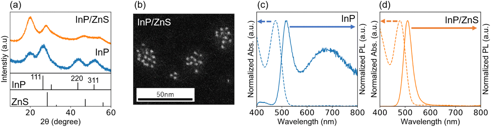 | ||
| Fig. 1 (a) XRD patterns of the core InP and the coherent InP/ZnS core/shell QDs capped with PA monolayers. Standard peak positions of InP and ZnS were assigned using ICDD PDF 00-032-0452 and 01-071-5975. (b) HAADF-STEM image of the coherent InP/ZnS core/shell QD capped with PA monolayers. UV–vis and PL spectra of (c) the core InP and (d) the coherent InP/ZnS core/shell QDs capped with PA monolayers. | ||
In general, a long-chain fatty acid or amine (i.e., oleylamine or oleic acid) is used in synthesis and works as a compact organic barrier bound to QDs, giving colloidal stability. However, the long-chain ligands minimize carrier mobility between QDs by increasing ligand-induced resistance.32,37 Therefore, such long chains are replaced with a short-chain ligand to narrow the interparticle distance between neighboring QDs. Short-chain thiol monolayer is a common capping ligand.38–41 The sulfur head group of the thiol ligand bonds to the surface cation of the QD with ionic strength stronger than the carboxyl head group of the fatty acid.42,43 Besides, colloidal stability is also maintained.44 Bai et al. reported that 6-mercapto-1-hexanol (MCH) as a capping ligand works to enhance the device performance.45 In this study, the PA ligand bound to the coherent InP/ZnS core/shell QD was replaced by MCH. As shown in Fig. 2(a), the PA-capped QDs dispersed in the hexane phase transferred to the ethanol phase due to the ligand exchange. The MCH-capped QDs were highly soluble in polar solvents such as DMF but insoluble in non-polar solvents. The QDs capped with PA were sticky due to the presence of long alkyl chains, but ligand exchange yielded QDs in dry powder form (see Fig. S1, ESI†). An XRD pattern shown in Fig. 2(b) demonstrates a decrease in the intensity of peak at ∼20° due to the substitution for the long-chain fatty acid with the short-chain thiol. Fig. 2(c) shows the ATR-FTIR spectra of the QD samples before and after ligand exchange. After ligand exchange, a broad band centered at 3283 cm−1, which is attributed to the hydroxyl group of the MCH ligand, appeared while the peak at 1550 cm−1, which is attributed to the symmetric carboxylate stretching vibration band,46 disappeared. The other peaks (1000–1500 cm−1) of the MCH-capped sample were confirmed to originate from the MCH molecule,45 indicating that the PA ligand was completely replaced by the MCH ligand. It is particularly noted that the insufficient ligand exchange affects film deposition on ITO-covered substrates. As evidenced in Fig. S2 (ESI†), we could not obtain a uniform QD film by dropping QD ink with inadequate ligand exchange.
 | ||
| Fig. 2 (a) Photograph of the colloidal dispersion of InP/ZnS QDs before and after ligand exchange. (b) XRD pattern of the InP/ZnS QD capped with the MCH monolayer. The peak intensity at 20° decreased by the ligand exchange. (c) ATR-FTIR spectra of the InP/ZnS QD before (upper), after ligand exchange (middle), and MCH solution (bottom). | ||
ATR-FTIR was used to examine whether the ligand exchange is sufficient or inadequate. Fig. S3† shows the ATR-FTIR spectrum of the QDs before and after the ligand exchange. Before ligand exchange (see blue spectrum), there was a peak at 1550 cm−1 attributed to the carboxyl group. The peak position was shifted to the shorter wavelength side compared to the free carboxyl group (1720 cm−1) due to ionic bonding with the metal cation.47 After ligand exchange (see the green spectrum), the peak of COO– disappeared whereas a new peak appeared at 3283 cm−1, which is attributed to the hydroxyl group of the MCH molecule. The absorbance was strong as high as the free MCH molecule (see the red spectrum). When the ligand exchange was inadequate (see the orange spectrum, Fig. S3†), the peak at 3283 cm−1 was weak. The decrease in QD film formability might be due to the aggregation of QDs caused by the difference in polarity of the ligands during the time between when the QD solution is dropped onto the substrate and when it completely dries. A similar aggregation was observed when ethanol was used instead of DMF. The results indicate that QD with both PA and MCH ligands causes a decrease in film formability.
As predicted, the film formation was hindered when this QD ink was used for device fabrication (see Fig. S4, ESI†). To avoid such a problem from arising, the PA-capped QDs were needed to be ultracentrifugally washed with acetone at least twice. The resultant PA-capped QDs were ligand exchanged and used as a QD ink capable of uniform film formation for device fabrication (see Fig. S2, ESI†). Hereafter, the coherent InP/ZnS QD capped with MCH is described by MCH-QD.
Fig. 3 shows schematically shows the device architecture of the photodiode in which the coherent InP/ZnS core/shell QD terminated with the MCH ligand serves as an optically active layer, the energy band diagram under voltage unbiased conditions and a cross-sectional SEM image. As shown in panel (a), the device has an inorganic multilayer stack (i.e., ITO/Al-doped ZnO/MCH-QDs/Al). A 22.5 nm thick Al-doped ZnO nanoparticle layer was deposited on an ITO-covered soda-lime glass substrate by a spin-coating method. Subsequently, a 100 nm thick MCH-QD layer was also formed by the spin-coating method. Finally, a 209 nm Al layer was deposited by vacuum evaporation at 2.0 × 10⁻⁵ Pa. Panel (b) shows the proposed energy level diagram under a zero applied voltage bias. The values of the work function of ITO and Al are taken from the literature.48 Based on the ultraviolet photoelectron spectroscopy (UPS) measurement of the spin-coated layer of Al-doped ZnO nanoparticles, the measured value of ionization energy was −7.12 eV (see Fig. S5 for more details, ESI†). The value of ionization energy for the MCH-QD layer, which was measured by photoelectron yield spectroscopy (PYS), was −5.7 eV (see Fig. S5, ESI†). The calculated value of electron affinity was −3.3 eV, assuming that the green photoemission originates from the fundamental optical gap of MCH-QDs. The Al-doped ZnO was inserted between the MCH-QD layer and the ITO electrode to create a type-II band alignment for exciton dissociation as depicted in panel (b). Panel (c) shows a cross-sectional SEM photograph of our QD-photodiode with good device performance. Unlike the device shown in Fig. S3 (ESI†), the 100 nm thick MCH-QD film is uniform and forms flat heterogeneous interfaces. In this device structure, we did not use organics to avoid the possibility of holes during device operation which degrade the device performance,49 leading to the long-running operation.
 | ||
| Fig. 3 (a) Device structure diagram of the MCH-QD film photodetector with an inorganic multi-layer stack. (b) Energy band diagram under unbiased conditions. (c) Cross-sectional SEM photographs of the multi-layer stack of the device. | ||
Device performances of the MCH-QD-based photodiode measured in ambient air are summarized in Fig. 4 and 5. Fig. 4(a) shows the room-temperature current–voltage curves under 470 ± 5 nm light irradiation. In a narrow measurement voltage ranging from −1.0 to 1.0 V, both forward and reverse scans were applied with steps of 0.02 V and a sweep time of 500 ms. Photocurrent generated was clearly dependent on the photon power of the irradiated light. Surprisingly, the photodiode also responded to even weak light with photon power equivalent to 0.29 mW cm−2. Photocurrent generated under the 470 nm light irradiation at zero voltage bias when the light power density varies from 0 to 11 mW cm−2 is shown in Fig. 4(b). The photocurrent increases linearly with power density of the incident light. Fig. 4(c) shows the responsivity of the device versus bias. Responsivity (R), a measure of the photocurrent generated per unit power of the incident light per unit area, was calculated from the equation: R = Ip/P,50 where Ip is the photocurrent subtracted from dark current, and P is the incident light power density. A trend of decreasing responsivity with increasing irradiation power density was observed, which might be due to the saturation of responsivity at high photon power irradiation.51 The detectivity, denoted by D*, was calculated from the equation: D* = R/(2eIdark/A)1/2, where e is the electron charge, A is the effective surface area, and Idark is the dark current, which is the main constituent of the shot noise current, respectively. As shown in Fig. 4(d), when the incident-light power density varied from 0.1 to 11 mW cm−2 at a bias of 1 V, the maxima of R and D* values were 15.6 mA W−1 and 8 × 10⁹ Jones (1 Jones = cm Hz1/2 W−1) at the incident-light power density of 0.43 mW cm−2, respectively.
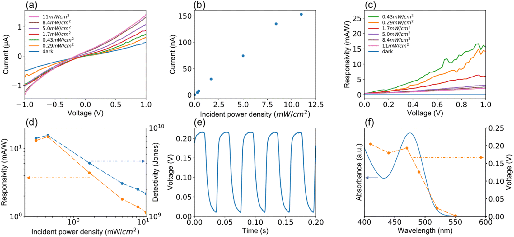 | ||
| Fig. 4 Summary of room-temperature device performances for the MCH-QD photodiode measured under 470 ± 5 nm light illumination at a voltage bias of 0 V (except for the panels (a) and (c)) in ambient air. (a) Changes in photocurrent at different light power densities when the voltage bias varies between −1.0 and 1.0 V. (b) Plots of photocurrent as a function of incident power density. (c) Changes in responsivity with increasing light power density when the voltage bias varies between 0 and 1.0 V. (d) The light power density dependence of responsivity and detectivity. (e) A typical time response curve of photocurrent. (f) Plots of photocurrent at different wavelengths of incident light superimposed on the UV-vis spectrum of MCH-QD. The power density of the incident light was fixed at 10 mW cm−2 for panels (e) and (f). | ||
The temporal response is a critical parameter for the evaluation of the device performance of photodiodes that need the ability to follow fast-changing optical signals utilized in optical communications and image processing. In this study, the response speed was measured at a voltage bias of 0 V under irradiation of 470 nm light with a power density of 11 mW cm−2, where the turn on/off time of the incident light was switched using an optical chopper. As schematically illustrated in Fig. 3(a), the photocurrent signals were recorded using an oscilloscope. A typical result of the time response curve is shown in Fig. 4(e), where a quick and reproducible photocurrent response and good cycling stability were observed even at a voltage bias of 0 V. Furthermore, the response profile exhibits that the measured rise time (τr: from 10% to 90% of the saturated value) and fall time (τf: from 90% to 10% of the peak value) are 4 ms and 9 ms, the fastest among the visible photodetectors based on Cd-free QDs and Pb-free perovskite nanocrystals. In Fig. 4(f), the measured values of photocurrent are plotted when the incident light wavelength varied between 410 and 530 nm. The measurement was performed at a voltage bias of 0 V and the power density was fixed at 10 mW cm−2. A representative optical absorption spectrum of the MCH-QD is superimposed on the plots to assert the incident-light wavelength selectivity of the photodiode. The photocurrent reached a maximum value for light irradiation at 470 nm, decreased at longer wavelengths, and was below the detection limit when the light of 530 nm or longer was irradiated. As expected, the trend of photocurrent generated as a function of irradiation-light wavelength was similar to the UV-vis behavior of the MCH-QD, suggesting that a wavelength selectivity of light detection can be tuned by the QD size.
It is known that a good long-term optical switching behavior has still been a challenge for QD photodiodes. In this study, I–V measurements in the bias ranging between −1 and 1 V were repeated 100 times under irradiation of 470 nm light of 10 mW cm−2. During this running test, we observed good I–V characteristics for each repeating time as presented in Fig. 5(a). The I–V measurements were repeated many times with no change in device performance such as responsivity, waveform, and response time as evidenced in Fig. 5(b). As clearly shown in the inset, the current reversibly switches between high and low conductance with high stability and reproducibility even after 100 times as the light is turned on and off, indicating the successful long-term operation due to device stability.
 | ||
| Fig. 5 Device lifetime of the MCH-QD-based photodiode measured at a voltage bias of 0 V at room temperature in ambient air using a 470 ± 5 nm light with a power density of 10 mW cm−2. Variation of (a) photocurrent and (b) responsivity for different number of measurements. Time response curves as insets were measured at the 1st time and 100th times. Error bars were obtained as the standard deviation by measuring 10 samples. | ||
To date, Cd-free QDs and Pb-free perovskite nanocrystals have been developed to serve as light-absorbing layers in photodiodes and phototransistors, but they have faced the barrier of a slow response time of several hundred millisecond scale (especially, fall time, see Table 1).31,32,52–54 There are two possible reasons for the fast photo responses at a single millisecond level in this work (see Fig. 4(e)). First, the ligand exchange enabled us to prepare a flat film thicker than 100 nm by repeated spin-coating. Furthermore, the molecular replacement with MCH ligands alters the interparticle dielectric environment as well as tunnelling distance, possibly leading to enhanced carrier mobility. Second, we expected that the coherent core/shell QD structure contributes to the efficient dissociation of carriers generated in InP QDs. In this core/shell structure, the 3ML shell is thin enough for traversing the charge carriers from the core QD to the ZnS layer through a slope of energy gradient at this junction. In addition, the emergent defect-less interface between the core and the shell allows the photogenerated carriers to spread over the entire core/shell QD. The reduction of defects at heterogeneous interfaces leads to faster response time.9 By utilizing the type-II band alignment between Al-doped ZnO and the ZnS layers, electrons and holes could separate on ultrafast time scales for detection.
| Material | Wavelength (nm) | Structure | Rise (ms) | Fall (ms) | Detectivity (Jones) | Responsivity (A W−1) | Ref. |
|---|---|---|---|---|---|---|---|
| InP QDs/black phosphorus | 405 | PT | 5 | 120 | 4.5 × 10¹⁶ | 1 × 10⁹ | 31 |
| InP QD | 650 | PT | — | — | — | — | 32 |
| SnS2 QD/MoS2 | UV-NIR | PT | 100 | 100 | 4.75 × 10¹³ | 278 | 52 |
| ZnO-QDs/MoS2 | 635 | PT | 1500 | 1100 | 1.05 × 10¹¹ | 0.084 | 53 |
| Bi2S3 nanocrystals | UV-NIR | PC | 23 | 23 | — | 20 | 54 |
| This work | 470 | PD | 4 | 9 | 8.0 × 10 9 | 0.016 | — |
There is still room to further optimize the device structure to improve the detectivity or responsivity which were inferior to Cd-based photodiodes. To enhance the carrier dissociation at the heterogeneous interfaces, the electron transportation layer should be replaced by a thicker film while blocking the electron leakage from the light-absorbing layer is needed. Further improving the quality of the light-absorbing layer can be realized by atom capping of the core/shell QD surface and such surface engineering is a worthy challenge for further improving device performance.
4. Conclusions
Bulk crystals of group III–V semiconductors including GaN, InP, InAs, and InSb have superior electronic properties such as high electron mobility. Their QDs allow size-dependent tuning of the first exciton peak in the optical absorption spectrum on the basis of the effect of the quantum confinement. Thus, it is expected that the wavelength-selective photodetection is realized using the QDs (as the light absorbing layers) of (i) InAs and InSb for the NIR-SWIR light, (ii) InP for the visible light, and (iii) GaN for the UV light. Nevertheless, few papers have reported photodetectors using their QDs as light-absorbing layers. In the previous paper, we reported the colloidally synthetic conditions to create a coherent InP/ZnS core/shell QD structure with a single lattice constant of 0.56 nm. We found in this work that the coherent core/shell QD as a light absorbing layer works to fabricate a good vertical-type photodiode that could be operated at room temperature in ambient air, showing the fast speed response at single-digit millisecond scale (i.e., τr/τf = 4/9 ms). Furthermore, this device operated in the photovoltaic mode of the photodiode circuit (i.e., 0 V voltage bias), unlike the phototransistors that require a power source to operate.55 The finding of coherent InP/ZnS core–shell QDs working as a photosensitive layer of QD photodiodes suggests that other combinations of core and shell work giving a fast response speed for photodetection.Author contributions
K. N. and N. S. designed the research; K. N. performed synthesis and characterization of QDs, and device fabrication and evaluation; J. W. optimized the experimental conditions for ligand exchange; H. Y. performed SEM to observe the cross-section of the device. K. N., H. S., and N. S. discussed the results, and K. N. and N. S. wrote the paper.Conflicts of interest
There are no conflicts to declare.Acknowledgements
The authors thank the Transmission Electron Microscopy Station of NIMS for HAADF-STEM observation and Yuka Hara for technical support of SEM observation. The authors thank OHSAWA Takeo of NIMS for technical support of the UPS measurements. This work was supported by the WPI program, JSPS KAKENHI Grant-in-Aid for Scientific Research (B) Grant Number 21H01910 and the Murata Science Foundation. H. T. thanks JSPS KAKENHI (Grant Number 21H01743 and 21K18942). H. Y. thanks the Research Fellow of JSPS and JSPS KAKENHI Grant-in-Aid for JSPS Fellows (Grant No. 20J23803).References
- T. Zhao, N. Oh, D. Jishkariani, M. Zhang, H. Wang, N. Li, J. D. Lee, C. Zeng, M. Muduli, H.-J. Choi, D. Su, C. B. Murray and C. R. Kagan, J. Am. Chem. Soc., 2019, 141, 15145–15152 CrossRef CAS PubMed.
- J. Leemans, V. Pejović, E. Georgitzikis, M. Minjauw, A. B. Siddik, Y. Deng, Y. Kuang, G. Roelkens, C. Detavernier, I. Lieberman, P. E. Malinowski, D. Cheyns and Z. Hens, Adv. Sci., 2022, 9, 2200844 CrossRef CAS PubMed.
- M. He, Z. Xu, S.-W. Zhang, M. Zhang, C. Wu, B. Li, J. Li, L. Wang, S. Zhao, F. Kang and G. Wei, Adv. Photonics Res., 2022, 2100305 CrossRef.
- J. H. Song, H. Choi, H. T. Pham and S. Jeong, Nat. Commun., 2018, 9, 4267 CrossRef PubMed.
- S. Yang, P. Zhao, X. Zhao, L. Qu and X. Lai, J. Mater. Chem. A, 2015, 3, 21922–21929 RSC.
- H. Li, W. Zhang, Y. Bian, T. K. Ahn, H. Shen and B. Ji, Nano Lett., 2022, 22, 4067–4073 CrossRef CAS PubMed.
- B. Ghosh, H. Yamada, S. Chinnathambi, İ. N. G. Özbilgin and N. Shirahata, J. Phys. Chem. Lett., 2018, 9, 5400–5407 CrossRef CAS PubMed.
- H. Jung, N. Ahn and V. I. Klimov, Nat. Photonics, 2021, 15, 643–655 CrossRef CAS.
- R. Guo, M. Zhang, J. Ding, A. Liu, F. Huang and M. Sheng, J. Mater. Chem. C, 2022, 10, 7404–7422 RSC.
- D.-Y. Guo, C.-X. Shan, S.-N. Qu and D.-Z. Shen, Sci. Rep., 2015, 4, 7469 CrossRef PubMed.
- H. Kan, W. Zheng, R. Lin, M. Li, C. Fu, H. Sun, M. Dong, C. Xu, J. Luo, Y. Fu and F. Huang, ACS Appl. Mater. Interfaces, 2019, 11, 8412–8418 CrossRef CAS PubMed.
- K. Shen, H. Xu, X. Li, J. Guo, S. Sathasivam, M. Wang, A. Ren, K. L. Choy, I. P. Parkin, Z. Guo and J. Wu, Adv. Mater., 2020, 32, 2000004 CrossRef CAS.
- J. Kim, S.-M. Kwon, Y. K. Kang, Y.-H. Kim, M.-J. Lee, K. Han, A. Facchetti, M.-G. Kim and S. K. Park, Sci. Adv., 2019, 5, eaax8801 CrossRef CAS PubMed.
- Y. Wei, Z. Ren, A. Zhang, P. Mao, H. Li, X. Zhong, W. Li, S. Yang and J. Wang, Adv. Funct. Mater., 2018, 28, 1706690 CrossRef.
- G. Sarasqueta, K. R. Choudhury, J. Subbiah and F. So, Adv. Funct. Mater., 2011, 21, 167–171 CrossRef CAS.
- T. Shen, B. Li, K. Zheng, T. Pullerits, G. Cao and J. Tian, J. Phys. Chem. Lett., 2018, 9, 3285–3294 CrossRef CAS PubMed.
- S. Mokkapati and C. Jagadish, Mater. Today, 2009, 12, 22–32 CrossRef CAS.
- P. Wen, P. Tiwari, S. Mauthe, H. Schmid, M. Sousa, M. Scherrer, M. Baumann, B. I. Bitachon, J. Leuthold, B. Gotsmann and K. E. Moselund, Nat. Commun., 2022, 13, 909 CrossRef CAS.
- X. Dai, S. Zhang, Z. Wang, G. Adamo, H. Liu, Y. Huang, C. Couteau and C. Soci, Nano Lett., 2014, 14, 2688–2693 CrossRef CAS PubMed.
- W. Liu, A. Y. Chang, R. D. Schaller and D. V. Talapin, J. Am. Chem. Soc., 2012, 134, 20258–20261 CrossRef CAS PubMed.
- M. Sotoodeh, A. H. Khalid and A. A. Rezazadeh, J. Appl. Phys., 2000, 87, 2890–2900 CrossRef CAS.
- Semiconductors and Semimetals, ed. S. C. Jain and M. Willander, Elsevier, 2003, vol. 74, pp. 91–145 Search PubMed.
- A. Dutta, M. K. Mukherjee and D. Mukhopadhyay, Czech J. Phys., 1991, 41, 474–483 CrossRef CAS.
- O. Madelung, U. Rössler and M. Schulz, Semiconductors: Group IV Elements, IV–IV and III–V Compounds. Part b – Electronic, Transport, Optical and Other Properties, Springer Materrials, 2002, vol. 41A1β Search PubMed.
- N. Kirkwood, L. De Trizio, A. W. Hoekstra, L. Kleibergen, N. Renaud, R. Koole, P. Baesjou, L. Manna and A. J. Houtepen, Chem. Mater., 2017, 29, 5192–5199 CrossRef PubMed.
- C. Dong, S. Liu, N. Barange, J. Lee, T. Pardue, X. Yi, S. Yin and F. So, ACS Appl. Mater. Interfaces, 2019, 11, 44451–44457 CrossRef CAS.
- S. J. Soenen, B. B. Manshian, T. Aubert, U. Himmelreich, J. Demeester, S. C. De Smedt, Z. Hens and K. Braeckmans, Chem. Res. Toxicol., 2014, 27, 1050–1059 Search PubMed.
- M. Yarema and M. V. Kovalenko, Chem. Mater., 2013, 25, 1788–1792 CrossRef CAS.
- H. Zhang, X. Ma, Q. Lin, Z. Zeng, H. Wang, L. S. Li, H. Shen, Y. Jia and Z. Du, J. Phys. Chem. Lett., 2020, 11, 960–967 CrossRef CAS PubMed.
- Y.-H. Won, O. Cho, T. Kim, D.-Y. Chung, T. Kim, H. Chung, H. Jang, J. Lee, D. Kim and E. Jang, Nature, 2019, 575, 634–638 CrossRef CAS PubMed.
- D.-H. Kwak, P. Ramasamy, Y.-S. Lee, M.-H. Jeong and J.-S. Lee, ACS Appl. Mater. Interfaces, 2019, 11, 29041–29046 CrossRef CAS PubMed.
- W. Liu, J.-S. Lee and D. V. Talapin, J. Am. Chem. Soc., 2013, 135, 1349–1357 CrossRef CAS PubMed.
- D. A. Taylor, J. A. Teku, S. Cho, W.-S. Chae, S.-J. Jeong and J.-S. Lee, Chem. Mater., 2021, 33, 4399–4407 CrossRef CAS.
- K. Nemoto, J. Watanabe, H.-T. Sun and N. Shirahata, Nanoscale, 2022, 14, 9900–9909 RSC.
- J. J. Calvin, T. M. Kaufman, A. B. Sedlak, M. F. Crook and A. P. Alivisatos, Nat. Commun., 2021, 12, 2663 CrossRef CAS PubMed.
- E. Cho, T. Kim, S. Choi, H. Jang, K. Min and E. Jang, ACS Appl. Nano Mater., 2018, 1, 7106–7114 CrossRef CAS.
- F. Hetsch, N. Zhao, S. V. Kershaw and A. L. Rogach, Mater. Today, 2013, 16, 312–325 CrossRef CAS.
- H. Seo, M. Bang, Y. Kim, C. Son, H. B. Jeon and S.-W. Kim, RSC Adv., 2020, 10, 11517–11523 RSC.
- P. Roy, G. Devatha, S. Roy, A. Rao and P. P. Pillai, J. Phys. Chem. Lett., 2020, 11, 5354–5360 CrossRef CAS PubMed.
- Z. Li, Y. Hu, H. Shen, Q. Lin, L. Wang, H. Wang, W. Zhao and L. S. Li, Laser Photonics Rev., 2017, 11, 1600227 CrossRef.
- D. Vasudevan, R. R. Gaddam, A. Trinchi and I. Cole, J. Alloys Compd., 2015, 636, 395–404 CrossRef CAS.
- J. Choi, W. Choi and D. Y. Jeon, ACS Appl. Nano Mater., 2019, 2, 5504–5511 CrossRef CAS.
- M. J. Turo and J. E. Macdonald, ACS Nano, 2014, 8, 10205–10213 CrossRef CAS PubMed.
- W. Lin, Y. Niu, R. Meng, L. Huang, H. Cao, Z. Zhang, H. Qin and X. Peng, Nano Res., 2016, 9, 260–271 CrossRef CAS.
- Z. Bai, W. Ji, D. Han, L. Chen, B. Chen, H. Shen, B. Zou and H. Zhong, Chem. Mater., 2016, 28, 1085–1091 CrossRef CAS.
- J. Simon-Kutscher, A. Gericke and H. Hühnerfuss, Langmuir, 1996, 12, 1027–1034 CrossRef CAS.
- Y. Ren, K. Iimura and T. Kato, Langmuir, 2001, 17, 2688–2693 CrossRef CAS.
- J. Watanabe, H. Yamada, H.-T. Sun, T. Moronaga, Y. Ishii and N. Shirahata, ACS Appl. Nano Mater., 2021, 4, 11651–11660 CrossRef CAS.
- H. Yamada, N. Saitoh, B. Ghosh, Y. Masuda, N. Yoshizawa and N. Shirahata, J. Phys. Chem. C, 2020, 124, 23333–23342 CrossRef CAS.
- M. Ahmadi, T. Wu and B. Hu, Adv. Mater., 2017, 29, 1605242 CrossRef PubMed.
- H.-S. Ra, D.-H. Kwak and J.-S. Lee, Nanoscale, 2016, 8, 17223–17230 RSC.
- C. S. R. Kolli, V. Selamneni, B. A. Muñiz Martínez, A. Fest Carreno, D. Emanuel Sanchez, M. Terrones, E. Strupiechonski, A. De Luna Bugallo and P. Sahatiya, ACS Appl. Mater. Interfaces, 2022, 14, 15415–15425 CrossRef CAS PubMed.
- Y. H. Zhou, Z. B. Zhang, P. Xu, H. Zhang and B. Wang, Nanoscale Res. Lett., 2019, 14, 364 CrossRef.
- G. Konstantatos, L. Levina, J. Tang and E. H. Sargent, Nano Lett., 2008, 8, 4002–4006 CrossRef CAS.
- C. Wang, X. Zhang and W. Hu, Chem. Soc. Rev., 2020, 49, 653–670 RSC.
Footnote |
| † Electronic supplementary information (ESI) available. See DOI: https://doi.org/10.1039/d2na00734g |
| This journal is © The Royal Society of Chemistry 2023 |