
Correlating multimode strain and electrode configurations for high-performance gradient-index phononic crystal-based piezoelectric energy harvesting†
Dae-Su
Kim
a,
Wonjae
Choi
bc,
Sun-Woo
Kim
a,
Eun-Ji
Kim
a,
Sahn
Nahm
 *a and
Miso
Kim
*d
*a and
Miso
Kim
*d
aDepartment of Materials Science and Engineering, Korea University, Seoul 02841, Republic of Korea. E-mail: snahm@korea.ac.kr
bIntelligent Wave Engineering Team, Korea Research Institute of Standards and Science, Daejeon 34113, Republic of Korea
cDepartment of Precision Measurement, University of Science and Technology (UST), Daejeon 34113, Republic of Korea
dSchool of Advanced Materials Science and Engineering, Sungkyunkwan University (SKKU), Suwon 16419, Republic of Korea. E-mail: smilekim@skku.edu
First published on 2nd November 2022
Abstract
A gradient-index phononic crystal (GRIN PnC) capable of manipulating wave propagation can serve as an excellent input wave energy focusing platform for amplifying energy harvesting power generation. However, despite its remarkable focusing capability, the finite wavelength of the propagating elastic waves in the focal area causes voltage cancellation inside a piezoelectric element under multimode strains having opposite directions; this limits the capacity of the GRIN PnC-based energy harvesting system. This study demonstrates a rational electrode configuration for a piezoelectric energy harvesting (PEH) device that can maximize the performance of a given GRIN PnC platform. The multimode strain analysis experimentally performed on the PEHs distributed over the focusing area confirms that the patterned electrode PEH configuration is the most effective in alleviating strain and voltage cancellation while efficiently transferring the focused elastic wave energy. Furthermore, a proper combination of electrical connections between the patterned electrodes substantially increases the piezoelectric potential across the ceramic by maximizing the strain difference. The simultaneous tailoring of the piezoelectric ceramic composition and the electrode configuration leads to a maximum power generation of 7.06 mW even under off-resonance conditions, the largest ever reported in elastic wave energy harvesting.
New conceptsThe demand for sustainable power sources has tremendously increased as required for the small wireless sensor modules for the Internet of Things. Piezoelectric energy harvesting (PEH) offers an attractive, green power solution by converting ambient sources in nature, otherwise wasted, such as sound, vibration and human kinetic motions, to generate useful electricity. However, insufficient power generation for practical application still remains a key challenge. Beyond disruptive approaches of high-performance energy conversion materials, devices, and high-efficiency power management circuits, phononic crystals and metamaterials offer a new paradigm of EH systems that pushes the boundaries to drastic harvesting performance enhancement through the amplification of input mechanical wave energy toward the desired location. Although a number of intriguing metamaterial designs have recently been proposed for metamaterial-based PEH, little attention has been paid to the proper design of piezoelectric materials and devices suitable for such phononic crystal- or metamaterial-assisted EH. In this regard, we identified the proper design of PEH devices particularly suitable for gradient-index phononic crystal (GRIN PnC)-based EH system, based on a systematic analysis of multimode strains. The proposed GRIN PnC-based PEH system with a patterned electrode configuration yields an unprecedented harvesting power output performance of 7.06 mW in elastic wave harvesting. |
1. Introduction
Nature has abundant energy resources including solar, wind, ocean, vibration, and sound energy, as well as human motions. When harvested, these resources can provide essential power generation for small electronics, such as sensors in a wide variety of industrial, wearable, and biomedical applications.1–7 Energy harvesting (EH) enables sustainable power generation by converting ambient input energy resources from the environment, which are otherwise unused, into valuable electrical energy. However, despite the high demand for EH, insufficient power generation for practical usage remains a challenge in this field. To boost the overall power output performance, innovative device designs,8–10 high-performance energy conversion materials,11–13 and disruptive power management circuits13,14 are required to increase the energy efficiency in each step of the energy transfer and conversion in EH: mechanical to mechanical coupling efficiency for enhanced energy, mechanical to electrical energy conversion efficiency, and electrical to electrical coupling efficiency through power management.Piezoelectric materials offer highly efficient and direct mechanical to electrical energy conversion capability within a compact volume; thus, they have been widely explored for energy harvesting.15,16 Piezoelectric materials with high dij × gij, the product of the piezoelectric charge coefficient dij and piezoelectric voltage coefficient gij, are highly desirable to yield high power output.12,16,17 A high-performance Pb(Zr,Ti)O3 (PZT), one of the most important engineering piezoelectric ceramic materials was developed to exhibit a morphotropic phase boundary (MPB) by tuning the solid-solution ratio of the rhombohedral PbZrO3(PZ) and tetragonal PbTiO3(PT) phases.18,19 A high dij × gij value was also achieved by tuning the proper composition of the (1 − x − y)PbZrO3–xPbTiO3–yPb(Ni1/3Nb2/3)O3 (PZ–PT–PNN) ceramic, where the PZ–PT–PNN ceramic must have a rhombohedral-tetragonal MPB structure close to the rhombohedral structure.12 In addition to compositional tuning, chemical doping, material texturing such as template grain growth,20,21 and transitioning to composite materials22 have been extensively adopted in various types of piezoelectric materials, including ceramics, single crystals, polymers, and composites at multi-scales.21–23 Structure-wise, piezoelectric materials develop piezoelectric potentials with opposite signs, depending on whether they are under tension or compression. If regions with opposite polarization orientations exist together within the same piezoelectric material, the developed voltages can cancel each other out. To avoid voltage cancellation, it is necessary to identify the strain nodes where the directions of the applied strain and the induced electrical fields are reversed inside the piezoelectric material during mechanical vibration. Based on multimodal strain analysis, various EH device designs such as segmented piezoelectric ceramics and patterned electrode configurations, whereby the strain node is not located within the same active piezoelectric layer, have been proposed.24–26
Beyond conventional energy harvesting research efforts on materials, devices, and circuits, a further disruptive approach for power enhancement in energy harvesting is required. Phononic crystals (PnCs) and acoustic metamaterials (AMMs) are artificially engineered structures with a remarkable wave manipulation capability owing to their unconventional properties, such as bandgap, negative bulk modulus, negative mass density, and negative refractive index.27–31 The controllability of acoustic and elastic wave propagation offers broad application prospects in the fields of acoustic cloaking,32 superlenses,28 waveguides,33 sound and vibration suppression,34 and energy harvesting.35,36 Using PnCs or AMMs, the input mechanical wave energies can be amplified to the desired point by controlling the wave propagation for focusing or localization.35,37,38 The amplified input energy is then delivered to the piezoelectric device for energy conversion, thereby realizing a significantly amplified power output overall. In the past few years, various intriguing concepts of metamaterials have actively been proposed, including PnCs with defects for wave energy localization,36,37 gradient index (GRIN) PnCs for focusing,35,39 acoustic metamaterials based on local resonances,40 mechanical metamaterials for vibration or sound energy isolation,34 and metasurfaces for phase-control-based energy confinement.41 When integrated with piezoelectric energy harvesting (PEH) devices and circuits, metamaterial-enabled energy harvesting systems demonstrate remarkably enhanced harvesting output performance. For example, as presented in our previous study,37 two-dimensional PnCs with an octagonal-shaped unit cell design enabled a substantial elastic wave localization at the defect owing to the bandgap, resulting in more than 20 times power enhancement. However, efforts into metamaterial-enabled energy harvesting are mostly devoted to pursuing innovative metamaterial designs that can serve as a platform for further amplification of the input wave energy. Nonetheless, the efficient transfer of the amplified input energy into a PEH device at the interface between the metamaterial and the PEH cannot occur without a proper design of a PEH device, irrespective of the quantity of the input energy that is amplified through a given metamaterial. However, notwithstanding the significance of identifying PEH devices suitable for each specific metamaterial design, little work has been reported thus far. Our previous study revealed that the geometric design of piezoelectric energy harvesters depends substantially on the wavelength and mechanical impedance of a given PnC with a defect.36 Based on these findings, a considerably enhanced power output amplification for the same given PnC platform was achieved by properly tailoring the material and geometric properties of the PEH device. Although useful, the study is limited to just defected PnC cases; it does not apply to other structures such as gradient-index phononic crystals (GRIN PnCs).
In this study, a rational patterned electrode configuration is optimized for the enhanced energy harvesting performance of a GRIN PnC-based PEH system. A GRIN PnC is an artificially designed periodic structure comprising several layers with spatially changing refractive indices. The GRIN PnC can modulate acoustic or elastic wave paths, offering a focusing capability for energy harvesting toward the target location.33,35,39 Once input elastic wave energy is focused, as illustrated in Fig. 1a, the amplified input mechanical energy is converted through piezoelectric energy harvesting devices to generate significantly enhanced electrical output power/energy overall (Fig. S2, ESI†). However, because GRIN PnC does not focus to a point but rather to a distributed area, strain and voltage cancellation can occur within the PEH device attached to the focusing area. This can reduce the harvesting output voltage and power performance. To identify the proper electrode and piezoelectric ceramic configurations, three PEH designs that can minimize the strain and voltage cancellation effect owing to the finite wavelength of the GRIN PnC: an ordinary PEH (O-PEH), segmented PEHs (S-PEHs), and a patterned electrode PEH (P-PEH), were considered in this study, as illustrated in Fig. 1. In addition, multimode strain analysis was performed based on the experimentally measured wave propagation behavior of the GRIN PnC with different PEH cases, leading to the idea of different electrical connections between the electrodes of the P-PEHs. The correlation between the applied strain and the developed piezoelectric potential is thoroughly analyzed, which underpins the most significant power output performance of the P-PEH with cross-electrical connections. Finally, with the best electrode configuration, the effect of both lead-containing and lead-free ceramics on the harvesting power output of GRIN PnC-based EH systems were studied. Tailoring the ceramic and electrode designs of the PEH enables power maximization up to 7.06 mW, which is the largest ever reported in elastic wave energy harvesting for the given GRIN PnC.
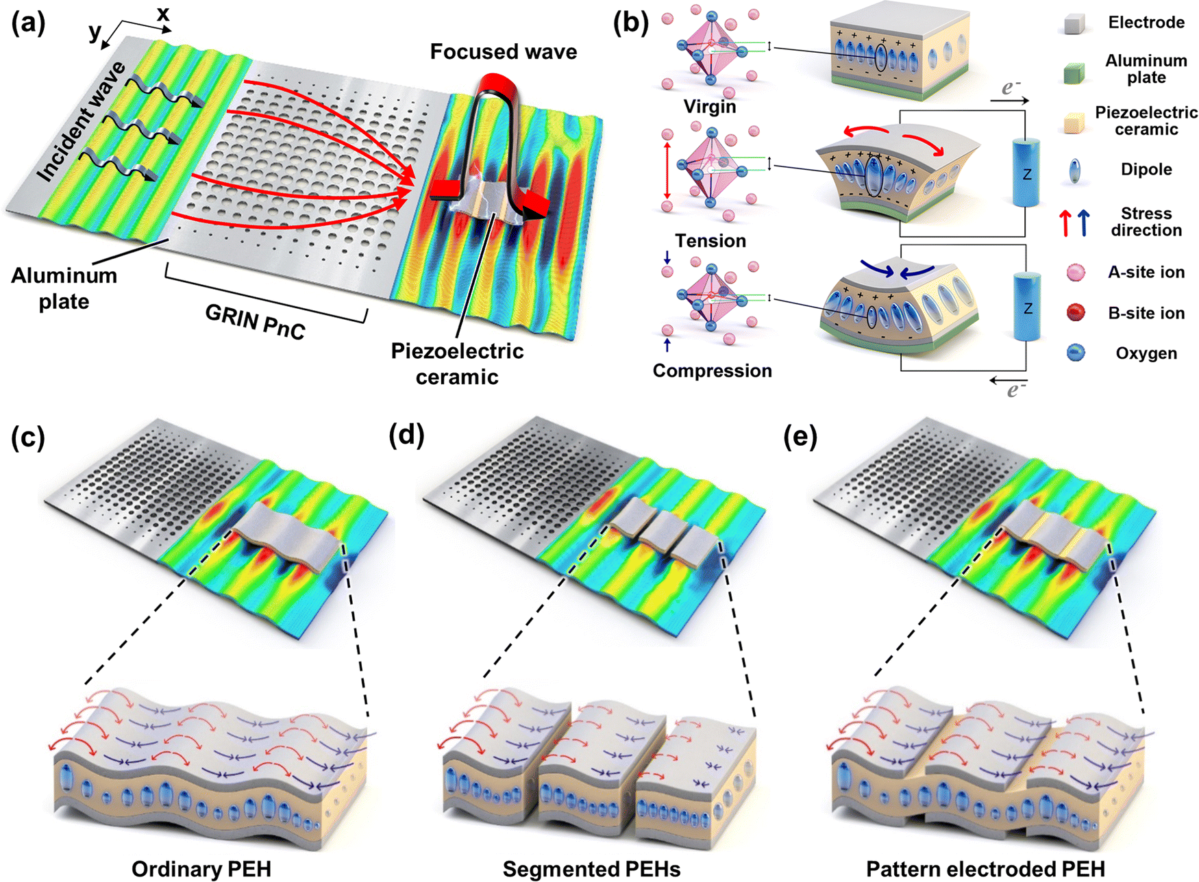 | ||
| Fig. 1 Schematic of a gradient-index phononic crystal (GRIN PnC)-based piezoelectric energy harvesting system: (a) visualization of the wave propagation behavior in the GRIN PnC as an elastic wave energy focusing platform. (b) Illustration of the relative change in the polarization state depending on the stress states: without external stress (virgin state), electrical charge generation under tensile stress and under compressive stress. Illustrations of the distribution of dipoles induced inside the piezoelectric ceramic beam in three different electrode/ceramic configurations: (c) an ordinary piezoelectric ceramic (O-PEH), (d) segmented piezoelectric ceramics and electrodes (S-PEH), and (e) a patterned electrode piezoelectric ceramic (P-PEH). | ||
2. Results and discussion
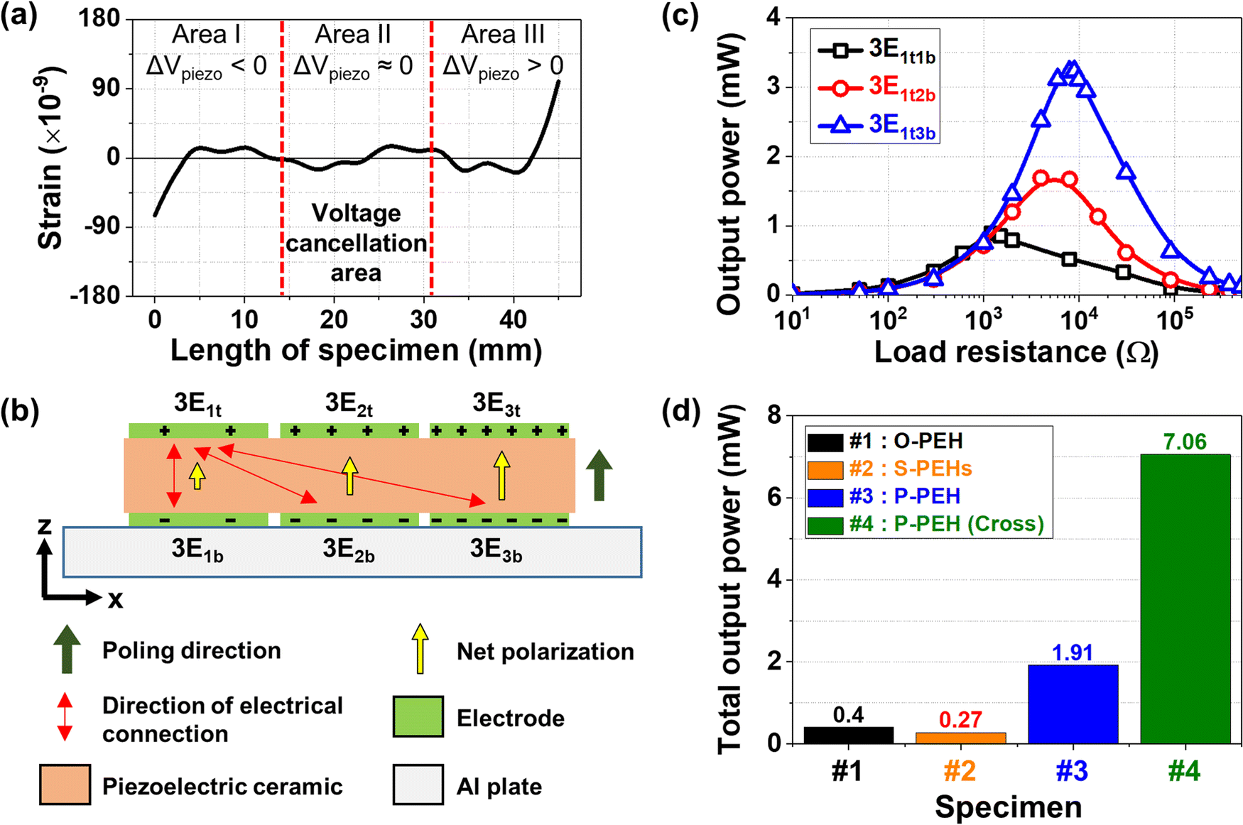
Fig. 1a shows a schematic of the GRIN PnC-based EH system. The same GRIN PnC designed in our previous study35 was used as the fixed platform. Circular hole-type unit cells of the GRIN PnC were systematically designed using a two-dimensional Reissner–Mindlin plate model and a genetic algorithm, which is described in ref. 35 in detail. Briefly summarize, the refractive index profile follows a hyperbolic secant profile, varying from 1 to 1.162 by controlling the circular hole radius from 0 to 2 mm of the square unit cell over the 17 layers (Fig. 1a). The incident plane waves at 50 kHz approach from the left side of the GRIN PnC of a 2 mm thick aluminum plate; prominent focusing occurs behind the GRIN PnC lens, where a PEH is attached. A piezoelectric ceramic disc was previously used35 as an EH device, the size of which was sufficiently smaller than half the wavelength to avoid voltage cancellation. In this study, a rectangular beam-type PEH device with a length that is significantly longer than several wavelengths is selected to cover the entire distributed entire focal area developed by the GRIN PnC and to observe the coexistence of multimode strains. Fig. 1b depicts the cross-section of the piezoelectric ceramic 0.32PZ–0.39PT–0.29PNN (PZT–PNN) with the top and bottom electrodes, where the relative change in the polarization state depending on the stress is indicated. In a virgin state with no applied stress, the intrinsic permanent polarization is associated with the noncentrosymmetric perovskite crystal structure of PZT–PNN. Note that PZT is only indicated as a representative case for simplicity. Under tension, the B-site cation (Zr4+ or Ti4+) displaces further toward the top surface owing to the unit cell volume expansion, resulting in larger dipoles and polarization than those of the virgin state. The change in the electric potential affected the surface charge distribution, resulting in an electrical current flowing from the top electrode to the bottom electrode. Under compression, the perovskite unit cells are suppressed, creating smaller dipoles and reduced polarizability compared to those in the virgin state. This generates current and voltage opposite to those of the tension case. Under the propagation of an elastic wave with a wavelength λ, the PEH device larger than the length of 2λ undergoes both temporally and spatially periodic sinusoidal out-of-plane displacements and experiences both tension and compression; this can cause voltage cancellation within the same ceramic.Fig. 1c–e illustrates the distribution of the dipoles induced inside the piezoelectric ceramic beam in three different electrode/ceramic configurations under elastic wave propagation. First, the O-PEH is a simple capacitor-type device that consists of a single ceramic, with a length L = 45.5 mm (>2λ) and a width w = 18 mm, sandwiched by a pair of top and bottom electrodes of the same size as the piezoelectric ceramic (Fig. 1c). Considerable voltage cancellation is expected in the O-PEH owing to the spatially periodic tension and compression inside. Next, in the nS-PEHs, n multiple PEH pieces with a gap of 1.75 mm in-between are attached in series to cover the same area of L × w as the O-PEH. In Fig. 1d, the 3S-PEHs with n = 3 are depicted. In the S-PEH configuration, each PEH segment can generate electrical output independently with a lower degree of strain cancellation, as each piece is within less than one wavelength. Finally, in Fig. 1e, a single piezoelectric ceramic covered by a pair of “patterned” electrodes–electrode area divided by n (∼L/n) – comprises the nP-PEH. In the nP-PEH, the area under the gap between the electrodes becomes electrically inactive, similar to the S-PEH, whereas the ceramic part mechanically undergoes periodic tension and compression, similar to the O-PEH. The advantage of the patterned electrode configuration is the substantial flexibility in varying the electrical connection combination. Note that the entire area covered by a PEH or multiple PEHs is kept the same for all three cases for a fair comparison.
Fig. 2a and c show how elastic waves propagate through the O-PEH and 3S-PEHs, respectively, based on the relative amplitude and direction of the measured out-of-plane displacement. It was experimentally confirmed that elastic waves travel over an area larger than 2λ without any discontinuity in the O-PEH. The blue- and red-colored areas correspond to the parts under compression and tension, respectively, each having a length of approximately λ/2 (Fig. 2a). Thus, mechanical stress is inevitably applied in opposite directions, causing voltage cancellation, as expected. Consequently, the O-PEH, the device without any design consideration of strain and voltage cancellation, generates an overall power output of 399 μW, as shown in Fig. 2b. In contrast, elastic wave propagation over a length smaller than 1λ was observed in each PEH segment of the 3S-PEHs, as shown in Fig. 2c. Therefore, each segment experiences only a single mode of strain, either tension or compression, which corresponds to the single-colored area of each segment in Fig. 2c. This suits the purpose of the S-PEH design, which is to avoid strain and voltage cancellation within the piezoelectric ceramic. The harvesting output electrical performance of each PEH segment of the 3S-PEHs, denoted as 3S1t1b, 3S2t2b, and 3S3t3b in the order of the closest distance from the incident waves, is characterized, and the results are shown in Fig. 2d. Notably, although strain cancellation is avoided by segmentation, much smaller power output is achieved in all three PEH devices – 3S1t1b, 3S2t2b, and 3S3t3b: 209 μW, 50 μW, and 15 μW, respectively. Furthermore, the sum of output powers from the three PEH devices is 274 μW, which is still smaller than that of the O-PEH. This is because segmentation into three pieces creates more physical boundaries, which causes the propagating waves to reflect backward considerably rather than to transmit into the PEH device, as experimentally confirmed in Fig. S3b (ESI†). For the same reason, the farther the segmented device is located from the GRIN PnC, the smaller the generated power output. Elastic waves are substantially attenuated through the first physical barrier, 3S1t1b, from which elastic waves with much-reduced intensity are transferred to 3S2t2b, which also acts as a barrier, and so on. Interestingly, because the 3S1t1b segment only experiences a single mode of strain, it undergoes a slightly larger deformation than O-PEH, generating a slightly larger output voltage (Fig. S4, ESI†). However, the power output of 3S1t1b is much smaller than that of O-PEH because of the one-third reduced active area. The reduced active area decreases the capacitance of 3S1t1b, resulting in an increase in electrical impedance and a decrease in output power.42
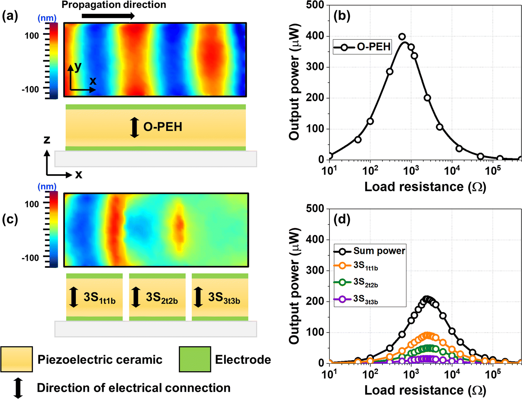 | ||
| Fig. 2 Experimental visualization of elastic wave propagation and harvesting power output in the O-PEH and 3S-PEHs: (a and c) out-of-displacements (z) measured using scanning Laser Doppler vibrometer inside the O-PEH and 3S-PEHs, respectively along with corresponding PEH schematics. (b and d) Power output with respect to the load resistance of the O-PEH and 3S-PEHs, respectively. | ||
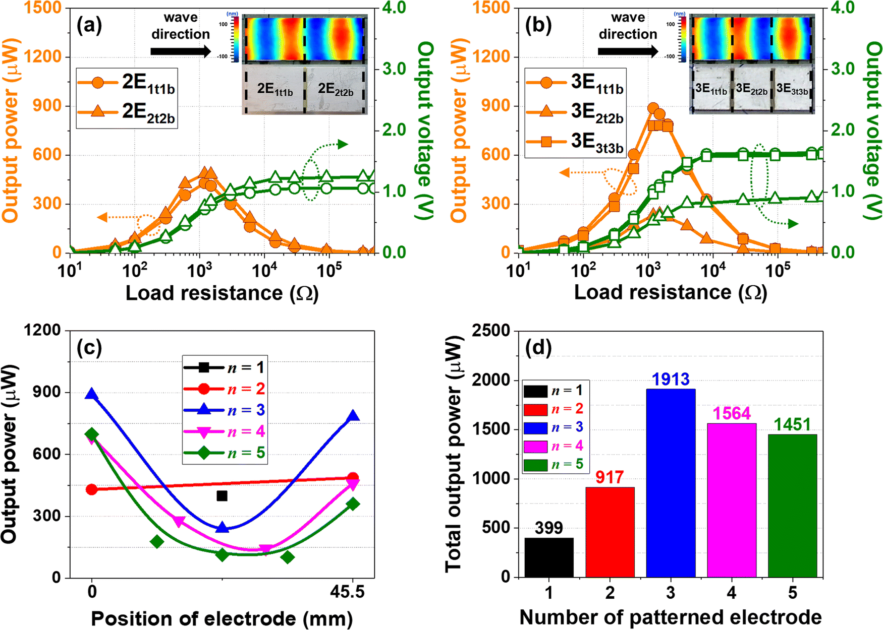
As an alternative, the nP-PEH device is proposed as a solution to mitigate voltage cancellation without any physical barrier for wave propagation within the ceramic. The entire top and bottom surfaces of the piezoelectric ceramic were divided into n regions (n = 1, 2, 3, 4, 5), such that n electrode segments compose the top and bottom surfaces (Fig. S5, ESI†). nEit and nEib, represent the ith electrodes on the top surface and bottom of the nP-PEH, respectively; nEitEjb indicates the case when the top ith and bottom jth electrodes are electrically connected. Fig. 3a and b show the harvesting output voltage and power measured from each electrical connection of the 2P-PEH and 3P-PEH devices, respectively, while the results for 4P-PEH and 5P-PEH are provided in Fig. S6 (ESI†). In the 2P-PEH, the opposite stress conditions coexist inside each area of 2E1t1b and 2E2t2b as indicated by the half-blue and half-red color in the inset of Fig. 3a. Nevertheless, a patterned electrode configuration proved advantageous in alleviating the strain cancellation effect to a certain degree, resulting in enhanced power output. Notably, 2E1t1b and 2E2t2b yield similar power output magnitudes of 430 μW and 487 μW, respectively, which are slightly larger than that of 1E1t1b (![[double bond, length as m-dash]](https://www.rsc.org/images/entities/char_e001.gif) O-PEH). Moreover, the total power from the 2P-PEH (917 μW) is 2.3 times higher than that of 1E1t1b. In the 3P-PEH, the electrode gaps are observed to align more with the boundary at which the state of stress exists, as shown in the inset of Fig. 3b. A single blue- or red-colored area in 3E1t1b and 3E3t3b indicates a prominent reduction in the strain cancellation effect, which is associated with the substantially enhanced power output from 3E1t1b and 3E3t3b.
O-PEH). Moreover, the total power from the 2P-PEH (917 μW) is 2.3 times higher than that of 1E1t1b. In the 3P-PEH, the electrode gaps are observed to align more with the boundary at which the state of stress exists, as shown in the inset of Fig. 3b. A single blue- or red-colored area in 3E1t1b and 3E3t3b indicates a prominent reduction in the strain cancellation effect, which is associated with the substantially enhanced power output from 3E1t1b and 3E3t3b.
 | ||
| Fig. 3 Output power at various load resistances (a) the 2P-PEH and (b) the 3P-PEH devices when the respective facing top and bottom electrodes are directly connected like simple capacitors (e.g., nEitEjb). Insets show photo images and laser Doppler vibrometer scanned results of 2P-PEH and 3P-PEH devices, respectively. (c) Variation of the power output of all nP-PEH devices depending on the electrode position. (d) Variation of the total power output in all 5 cases of the nP-PEH devices. | ||
Meanwhile, the coexistence of the opposite stress conditions within the same piezoelectrically active region accounts for the generation of much lower power output from 3E2t2b, the middle region, even compared to O-PEH. Notably, it is consistently observed in all nP-PEH devices that the middle region yielded the lowest output power, while the regions at both ends produced the largest output power (Fig. 3c). This observation is due to the voltage cancellation effect. The considerable power generation at both ends is attributed to the accumulation of reflected waves at the ceramic wall.43 Once elastic waves are transferred from the GRIN aluminum plate to the ceramic, the transmitted elastic waves encounter the wall of the ceramic at the interface between the ceramic and aluminum plate, where both transmission and reflection occur. The reflected waves propagate back in the opposite direction and then encounter the ceramic wall on the other side. The repetitive reflection at both ends results in the accumulation of elastic wave energy, which can be converted into electric energy through piezoelectricity.
Overall, the 3P-PEH case proved to be the most effective in maximizing the harvesting power for the given GRIN-enabled system. In the plain parallel electric connections, the total power output of the 3P-PEH reaches up to 1.91 mW, which is 4.8 times larger than that of the O-PEH, proving the effectiveness of the patterned electrode configuration. It should be noted that the 4P-PEH generates a smaller total output power than the 3P-PEH despite its higher output voltage generation (Fig. 3d and Fig. S6a, ESI†). However, the matching electrical impedance of the piezoelectric ceramic increases as the electrode area of each region reduces, thus significantly decreasing the output power of each ceramic piece and the total output power of the 4P-PEH.
To further investigate the strain behavior inside the piezoelectric ceramic under elastic wave propagation, the strain distribution in the 3P-PEH at discrete times over one cycle (= λ) is derived, and the results are shown in Fig. 4. Fig. 4a shows a phase difference of ∼π/2 between the output voltage and the corresponding mechanical displacement in the time domain when the maximum power is produced from the 3P-PEH device in the plain parallel electric connections (3E1t1b, 3E2t2b, and 3E3t3b), at its power-optimal electrical resistance of 1.5 kΩ. Thirteen points (in time) that can sufficiently cover one wavelength of the sinusoidal voltage signal are selected, as indicated in Fig. S7 (ESI†). At each of these points, out-of-plane (x–z) mechanical displacement curves are extracted and then differentiated twice to calculate the strain along the centerline of the ceramic (Fig. S8, ESI†). Five representative cases are shown in Fig. 4b–f. Consistent with the observation made in Fig. 3, the middle part of the ceramic simultaneously undergoes mechanical strains in opposite directions with extremely small magnitudes, accounting for the strain and voltage cancellation and the resulting low output power in this area.
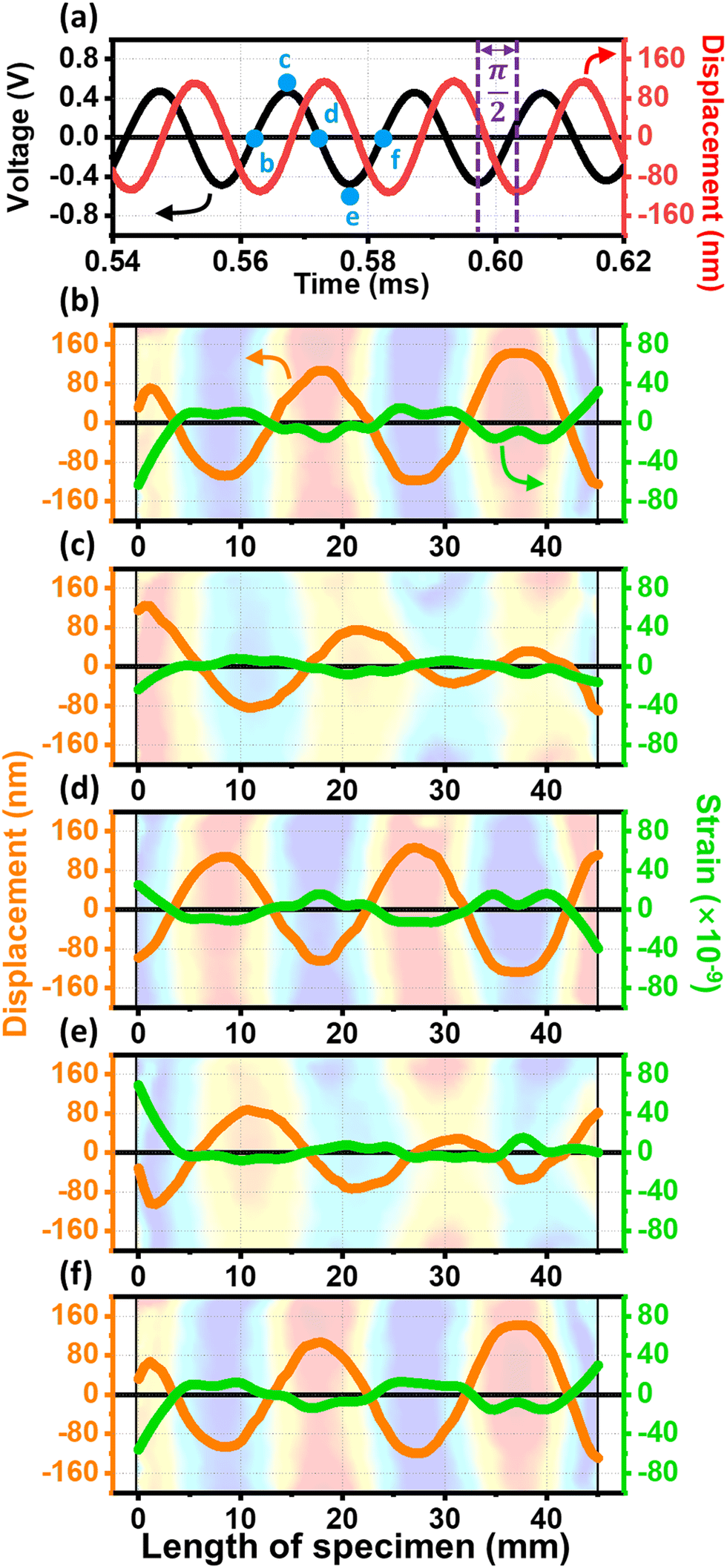 | ||
| Fig. 4 (a) Phase difference between the measured output voltage and the out-of-plane mechanical displacements of the 3P-PEH device in the time domain. (b–f) Measured out-of-plane mechanical displacement (z) curves and the corresponding strain curves calculated along the centerline of the 3P-PEH device at time t: (b) t = 0.5822 ms, (c) t = 0.5872 ms, (d) t = 0.5922 ms, (e) t = 0.5972 ms, and (f) t = 0.6023 ms. | ||
Interestingly, relatively very high strain values repeatedly appear at both ends over time, as shown in Fig. 4b and f, which is responsible for the higher output power in these regions, as shown in Fig. 3. As mentioned earlier, this is attributed to the internal reflection of elastic waves at the boundaries of the ceramic. Most importantly, there is a clear difference between the strain values, although with opposite signs, at both ends over time (Fig. 4b–f and Fig. S8, ESI†).
The above observation suggests a great possibility that we can further boost the piezoelectric potential difference across a ceramic by connecting the top and bottom electrodes in different combinations. Considering the largest strain difference between the electrode ends, it can be postulated that an enormous piezoelectric potential difference can be induced to drive the most significant number of surface charges to move through when a top electrode at one end is cross-connected to a bottom electrode at the other end (e.g., 3E1t3b). Fig. S9 (ESI†) demonstrates the relation between the mechanical displacement and voltage in the time domain, where the two are in phase. Fig. S10 (ESI†) shows the calculated strain distribution along the centerline of the piezoelectric ceramic in the 3E1t3b configuration over one cycle of 1λ, where the same trends of strain behavior as the parallel connection (3E1t1b) are observed, independent of the electrical connection.
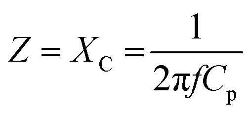
As shown in Fig. 5a (reproduced from the 10th point of Fig. S9 and S10, ESI†), a negative strain with the maximum magnitude is dominant in Area I, which is associated with a negative potential difference (ΔVpiezo < 0) with a reduced net polarization. Likewise, the largest positive strain is predominant in Area III, corresponding to a relatively large net polarization inside the ceramic, thus creating a higher number of surface charges. Therefore, there is a substantially high positive internal potential difference (ΔVpiezo > 0) in Area III. In contrast, because of the coexistence of opposite strains, the net polarization approaches zero (ΔVpiezo ≈ 0) in Area II. For comparison, three different combinations of electrical connections, 3E1t1b, 3E1t12b, and 3E1t3b, illustrated in Fig. 5b – are tested for harvesting output performance; the results are shown in Fig. 5c. The cross-connected 3E1t3b case yielded the maximum output power of 3.22 mW, although the increasing distance between the electrodes resulted in electrical loading across the ceramic. In increasing order of magnitude, the output power generation is 3E1t1b < 3E1t12b < 3E1t3b, which agrees with the increasing order of the internal polarization difference between the electrodes, supporting the postulation made. Notably, the output power of 3.22 mW achieved from the 3E1t3b case is as much as 7.0 times larger than that of 3E1t1b (463 μW). These results demonstrate the best way to maximize output power generation. Combining 3E1t3b, 3E2t2b, and 3E3t1b enables the 3P-PEH to produce a maximum total output power of 7.06 mW (Fig. S11 and Table S1, ESI†). Compared with the O-PEH, the 3P-PEH with optimal cross-electrical connections generates 17.7 times amplified output power in total, as demonstrated in Fig. 5d. One important aspect to note in Fig. 5c is that the power-optimal electrical impedance increases when the distance between the top and bottom electrodes becomes larger (3E1t1b < 3E1t2b < 3E1t3b). The optimum matching impedance of PEHs has the relationship of capacitance and the following eqn (1),
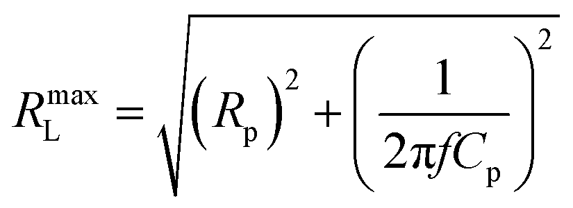 | (1) |
Therefore, the internal impedance (Z) of the piezoelectric ceramics has an inverse relationship with the capacitance. As longer distances between top and bottom electrodes coincide with a larger thickness of the ceramic between the electrodes as a capacitor, it yields reduced capacitance, in turn matching with higher impedance. Therefore, the power-optimal electrical impedance exhibits a higher value in 3E1t3b than in 3E1t1b. This is also experimentally confirmed by the results in Fig. S18 (ESI†).
 | ||
| Fig. 5 Correlation of strain distribution and the electrical connections in 3P-PEH: (a) strain distribution and associated piezoelectric potential difference along the centerline of the PEH. (b) Illustration of possible electrical connections between the top and bottom electrodes (red arrows) in the 3P-PEH device. (c) Power output of various electrical load resistances for each electrical connection, including the cross-connected 3E1t3b of the 3P-PEH device. (d) Overall comparison of the total power output for the PEHs with various electrode configurations. | ||
The proper selection of piezoelectric materials depending on the harvesting environment is essential. In mechanical vibration energy harvesting, several studies have consistently confirmed that piezoelectric materials with a high figure-of-merit dij × gij should be employed for output power maximization, particularly under off-resonant conditions. While very few studies exist on the correlation of piezoelectric materials to harvesting output performance, the same design principle of high figure-of-merit dij × gij for enhanced performance proved applicable to elastic wave energy harvesting in our previous studies.35,36 Meanwhile, in our other previous study,12 the optimal composition of the (1 − x − y)PbZrO3–xPbTiO3–yPb(Ni1/3Nb2/3)O3 (PZ–PT–PNN) ceramic was identified to be 0.32PZ–0.39PT–0.29PNN, which exhibited a sufficiently high d33 × g33 of 25.2 × 10⁻¹² m2 N−1. Interestingly, although PZT–PNN with other compositions, 0.16PZ–0.34PT–0.5PNN, exhibited a significantly high d33 of 855 pC N−1 at the rhombohedral–tetragonal–pseudocubic triple point, the dij × gij is not sufficient because of the high dielectric constant, which causes a reduction in gij (= dij/(εTij/ε0)) simultaneously.44 To achieve a high dij × gij value, it is necessary to significantly lower the dielectric constant, even if the dij value is partially sacrificed. Accordingly, 0.32PZ–0.39PT–0.29PNN, a soft-type lead-based ceramic (soft PZT) that slightly shifted from the MPB to the rhombohedral structure, was selected and fabricated for this study. For comparison, other compositions and constituent materials were selected to fabricate 3P-PEH devices consisting of three representative piezoelectric material types: a hard lead-based piezoelectric ceramic (hard PZT), a soft lead-free piezoelectric ceramic (soft KNN), and a hard lead-free piezoelectric ceramic (hard KNN). In the three representative piezoelectric ceramics, except for hard KNN, two or more phases coexist. For example, both hard PZT and soft PZT rhombohedral(R)–tetragonal(T) MPB structures, whereas soft KNN exhibits a polymorphic phase boundary structure in which orthorhombic(O) and T structures coexist.
Fig. 6a depicts the spontaneous polarization directions of the coexisting phases present in the four types of piezoelectric ceramics in the incident electric field along the [001] direction. The detailed material properties and characterization results are fully provided in Table 1 and Fig. S12–S14 (ESI†), respectively. While both Hard PZT and soft PZT exhibit the coexistence of tetragonal and orthorhombic phases, the relative composition of each crystalline phase differs, as indicated in Fig. 6a, resulting in discerning piezoelectric properties shown in Fig. S14 (ESI†). Likewise, for KNN, soft and hard piezoelectric properties are determined from the dominant crystalline orientation responsible for spontaneous polarization (Fig. 6a). All 3P-PEH devices consisting of the four types of piezoelectric ceramics with the same best cross-electrical connection combination were characterized for elastic GRIN-based wave energy harvesting (Fig. 6 and Fig. S15–S17, ESI†). First, Fig. 6(b) suggests that the increase in the dij × gij values leads to an increase in the total output power performance, confirming the validity of the piezoelectric material figure-of-merit dij × gij for elastic wave energy harvesting with multimode strains. As a result, the highest output power is achieved by the soft PZT, which is used in the aforementioned study. Second, in both Pb-based and Pb-free ceramics, soft piezoelectric materials are found to be much more advantageous than their hard counterparts in terms of elastic wave energy harvesting under off-resonance conditions, similar to vibration energy harvesting. The fundamental resonant frequencies of the ceramic devices would be far off the operating frequency of 50 kHz, as shown in Fig. S18 and S19 (ESI†), validating the off-resonance condition. It is noteworthy that the total output power of 7.06 mW is derived from harvesting elastic waves even under off-resonant conditions. Considering that only a few microwatts of output power can generally be obtained under off-resonance conditions in vibration energy harvesting,45,46 this milliwatt-level output power value is a remarkably enhanced yield. Third, another notable aspect is that the soft KNN with a 1.5 times higher d33 value yields a lower output power than the hard PZT. This is due to the 2.7-fold increase in the permittivity ε, contributing to lowering the overall dij × gij (= dij2/(εTij/ε0)) and the resulting output power.
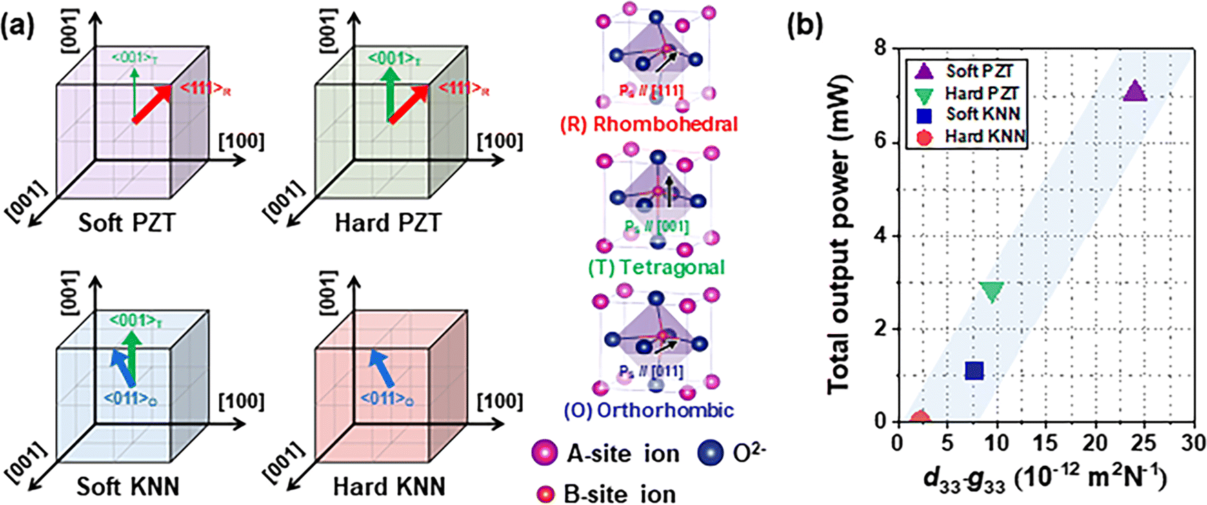 | ||
| Fig. 6 Four representative piezoelectric ceramics and their output performances: (a) dipole configurations and the crystal structure of the unit cell distortions in each of the rhombohedral, tetragonal, and orthorhombic structures in the following four representative piezoelectric ceramics: soft PZT, hard PZT, soft KNN, and hard KNN piezoelectric ceramics. (b) Total harvesting power output of the GRIN PnC-PEH systems as a function of piezoelectric figure-of-merit d33 × g33 values in the same 3P-PEH cross-connection electrode configurations. | ||
| Composition | Type | d 33 (pC N−1) | g 33 (10−3 Vm N−1) | ε T33/ε0 | k p | Q m | d 33 × g33 (10−12 m2 N−1) | |
|---|---|---|---|---|---|---|---|---|
| Lead-based ceramic | 0.32PbZrO3–0.39PbTiO3–0.29Pb(Ni1/3Nb2/3)O3 | Soft | 740 | 32.4 | 2580 | 0.61 | 50 | 24.0 |
| 0.8Pb(Zr0.51Ti0.49)O3–0.2Pb(Zn1/3Nb2/3)O3 + 0.5 wt% MnO2 | Hard | 330 | 25.4 | 1300 | 0.62 | 880 | 9.5 | |
| Lead-free ceramic | 0.96(K0.5Na0.5)(Nb0.89Sb0.11)O3–0.04CaZrO3 + 1.0 mol% CuO | Soft | 490 | 15.6 | 3540 | 0.45 | 27 | 7.7 |
| (K0.5Na0.5)(Nb0.995Fe0.005)O3 + 1.0 mol% CuO | Hard | 80 | 27.4 | 330 | 0.31 | 1900 | 2.2 | |
3. Conclusion
This study demonstrates rational patterned electrode configurations that can maximize the net polarization difference across a piezoelectric ceramic device for GRIN PnC-based elastic wave energy harvesting. To fully take advantage of the amplified input elastic wave energy by the focusing capability of the GRIN PnC, the voltage cancellation effect due to the coexistence of multimode strains with opposite directions was alleviated. Among the PEH devices with three different electrode configurations – O-PEHs, S-PEH, and P-PEH – particularly the 3P-PEH with a pair of three divided electrode patterns, proved to be the most effective in minimizing strain cancellation, while avoiding the creation of any further mechanical impedance, for efficient energy transfer from the GRIN plate to the PEH. The multimode strain analysis performed on the ceramic distributed over the focusing area under dynamic elastic wave propagation offers an idea to further increase the piezoelectric potential across the ceramic by connecting the electrode area with the largest strain difference. For the same optimal electrode pattern and connection configuration, four representative types of piezoelectric ceramic materials were fabricated via composition tuning and thoroughly compared in terms of harvesting performance. As a result, the total output power of 7.06 mW was achieved, which is 17.7 times larger than that of the ordinary PEH device, for the same GRIN PnC platform. To the best of our knowledge, this is the highest level of output power ever reported for elastic-wave energy harvesting. These findings would provide inspiration for the rational design of various phononic crystal- and metamaterial-based energy-harvesting systems with milliwatt-level power generation for practical applications.4. Experimental methods
Fabrication of soft-type lead-based piezoelectric ceramic
A 0.32PbZrO3–0.39PbTiO3–0.29Pb(Ni1/3Nb2/3)O3 [0.32PZ–0.39PT–0.29PNN] piezoelectric ceramic for GRIN PnC-based energy harvesting was prepared using conventional solid-state reaction methods. PbO (99.2%, Dansuk Industry, Korea), ZrO2 (99.2%, Z-Tech, USA), TiO2 (99.2%, Sakai Kagaku, Japan), NiO (99.2%, Nikko Rika, Japan), and Nb2O5 (99.2%, Jiujiang, China) were weighed and mixed by ball milling for 24 h in a Nalgene bottle containing anhydrous ethanol and yttria-stabilized zirconia balls. After ball milling, the powder mixtures were dried and calcined at 880 °C for 4 h. Subsequently, the calcined powders were ball-milled again for 72 h. Rectangle-type and disk-type compacts with dimensions of 45 × 18 × 3 mm and ∅12 × 1 mm, respectively, were formed by uniaxial pressing at 20 MPa. The green specimens were sintered at 1,150 °C for 2 h at a heating rate of 5 °C min−1 and cooled. After a silver paste was formed on both surfaces of the sintered specimens, the specimens were annealed at 600 °C for 10 min at a heating rate of 10 °C min−1, and then cooled in a furnace. In addition, hard PZT and soft and hard KNN materials were fabricated, as explained in the ESI.†Characterization of piezoelectric properties
The crystal structures of the sintered ceramic specimens were investigated by X-ray diffraction (Shimadzu, XRD-6100, Japan). The microstructures of the specimens were studied using field emission scanning electron microscopy (FE-SEM, Hitachi, S-4800, Japan). The poling process was performed by applying an electric field of 3 kV mm−1 to the specimens for 10 min at room temperature in a silicon oil bath for dipole alignment. Disk-type specimens were used to measure the piezoelectric and dielectric properties. The d33 values of the specimens were measured using a d33 meter (Micro-Epsilon Channel Product, DT-3300, USA), and the dielectric properties, piezoelectric voltage coefficient (g33), and electromechanical coupling factor (kp) were obtained using an impedance analyzer (Agilent Technologies, HP 4194A, USA), while the radial vibration modes were calculated using the resonance method.47 Polarization versus electric field (P–E) hysteresis curves and current density versus electric field (J–E) curves were measured using a ferroelectric tester (RT-66C, Precision, USA) with a high-voltage amplifier (Trek, 610E, USA). The P-E curves were measured at 1 Hz in silicon oil.Characterization of the piezoelectric energy harvesting performance
The GRIN PnC was used as a platform for elastic waves focusing upon incident plane waves at 50 kHz. The same experimental procedures were followed for elastic wave focusing characterization, as demonstrated in our previous study.35 Custom-designed cylinder-type piezoelectric transducers (Single Crystal PZT, Ceracomp Co. Ltd, Korea) with a resonant frequency of 50 kHz were attached to a GRIN aluminum plate with a thickness of 2 mm to generate incident elastic waves at 50 kHz. To induce a plane wave, the distance between the piezoelectric transducers and GRIN PnC must be at least 20 times larger than the wavelength of the incident wave. Thus, the transducers were located 500 mm away from the GRIN PnC supercell (Fig. S1, ESI†). For the input signal, a tone burst of 50 kHz with 20 cycles at intervals of 1 s was generated using a function generator (Keysight 33512 B, USA). To control the amplitude, the voltage of the function generator was set to be ±5 V for all experiments. The generated signal was amplified to an 85% gain level using an amplifier (AE-Techron 7224, USA) and input to a piezoelectric transducer. The out-of-plane mechanical displacement z of the GRIN aluminum plate was measured either at a point or over an area, using a scanning laser Doppler vibrometer (LDV, Polytec, PSV-400, OFV-5000, Germany). Regardless of the electrode type of the PEH devices, the maximum peak-to-peak amplitude of the out-of-plane mechanical displacement in the incident plane waves is observed to be 240 mm in all our LDV-scanned results. The ceramic beam-type PEH device of each configuration was attached to the region where the maximum focusing of the elastic waves occurs, based on the scanning LDV scan results (Fig. S20, ESI†). The output voltage generated by the PEH device was measured using an oscilloscope (Teledyne LeCroy, Waverunner 610zi, USA) for various load resistances. The power output was calculated using Ohm's law (output voltage)2/load resistance.Conflicts of interest
There are no conflicts to declare.Acknowledgements
This research was supported by the Basic Science Research Program through the National Research Foundation of Korea (NRF) grant funded by the Korean Government (MEST) (NRF-2021R1A2C2095767), and the Nano. Material Technology Development Program through the NRF funded by the Ministry of Science and ICT(NRF-2021M3A7C2089759), and the Technology Innovation Program (or Industrial Strategic technology development program, Project No. 20008775, Development of display integrated surface vibration and ecofriendly Pb-free piezoelectric materials and application technology) funded by the Ministry of Trade, Industry & Energy (MI, Korea).References
- Z. Yang, S. Zhou, J. Zu and D. Inman, Joule, 2018, 2, 642 CrossRef CAS.
- A. Petritz, E. Karner-Petritz, T. Uemura, P. Schäffner, T. Araki, B. Stadlober and T. Sekitani, Nat. Commun., 2021, 12, 1 CrossRef.
- L. Ruiz-Garcia, L. Lunadei, P. Barreiro and I. Robla, Sensors, 2009, 9, 4728 CrossRef.
- B. Shi, Z. Li and Y. Fan, Adv. Mater., 2018, 30, 1801511 CrossRef.
- X. Pu, W. Hu and Z. L. Wang, Small, 2018, 14, 1702817 CrossRef.
- S. Zeadally, F. K. Shaikh, A. Talpur and Q. Z. Sheng, Renewable Sustainable Energy Rev., 2020, 128, 109901 CrossRef.
- H. Wang, A. Jasim and X. Chen, Appl. Energy, 2018, 212, 1083 CrossRef.
- H. Liu, H. Fu, L. Sun, C. Lee and E. M. Yeatman, Renewable Sustainable Energy Rev., 2021, 137, 110473 CrossRef.
- S. F. Leung, Q. Zhang, M. M. Tavakoli, J. He, X. Mo and Z. Fan, Small, 2016, 12, 2536 CrossRef CAS PubMed.
- B. Chen, W. Tang and Z. L. Wang, Mater. Today, 2021, 50, 224 CrossRef CAS.
- T. Zhu, C. Fu, H. Xie, Y. Liu and X. Zhao, Adv. Energy Mater., 2015, 5, 1500588 CrossRef.
- T. G. Lee, H. J. Lee, S. W. Kim, D. H. Kim, S. H. Han, H. W. Kang, C. Y. Kang and S. Nahm, J. Eur. Ceram. Soc., 2017, 37, 3935 CrossRef CAS.
- S. Priya, H.-C. Song, Y. Zhou, R. Varghese, A. Chopra, S.-G. Kim, I. Kanno, L. Wu, D. S. Ha and J. Ryu, Energy Harvesting Syst., 2017, 4, 3 CrossRef.
- H. Lhermet, C. Condemine, M. Plissonnier, R. Salot, P. Audebert and M. Rosset, IEEE J. Solid-State Circuits, 2008, 43, 246 Search PubMed.
- C. Chen, X. Wang, Y. Wang, D. Yang, F. Yao, W. Zhang, B. Wang, G. A. Sewvandi, D. Yang and D. Hu, Adv. Funct. Mater., 2020, 30, 2005141 CrossRef CAS.
- H. C. Song, S. W. Kim, H. S. Kim, D. G. Lee, C. Y. Kang and S. Nahm, Adv. Mater., 2020, 32, 2002208 CrossRef CAS.
- S. W. Kim, T. G. Lee, D. H. Kim, K. T. Lee, I. Jung, C.-Y. Kang, S. H. Han, H.-W. Kang and S. Nahm, Nano Energy, 2019, 57, 581 CrossRef CAS.
- T. Y. T. Yamamoto, Jpn. J. Appl. Phys., 1996, 35, 5104 CrossRef CAS.
- M. Ahart, M. Somayazulu, R. Cohen, P. Ganesh, P. Dera, H.-k Mao, R. J. Hemley, Y. Ren, P. Liermann and Z. Wu, Nature, 2008, 451, 545 CrossRef CAS PubMed.
- Y. Saito, H. Takao, T. Tani, T. Nonoyama, K. Takatori, T. Homma, T. Nagaya and M. Nakamura, Nature, 2004, 432, 84 CrossRef CAS PubMed.
- Y. Yan, K. H. Cho, D. Maurya, A. Kumar, S. Kalinin, A. Khachaturyan and S. Priya, Appl. Phys. Lett., 2013, 102, 042903 CrossRef.
- S. Mishra, L. Unnikrishnan, S. K. Nayak and S. Mohanty, Macromol. Mater. Eng., 2019, 304, 1800463 CrossRef.
- G. T. Hwang, H. Park, J. H. Lee, S. Oh, K. I. Park, M. Byun, H. Park, G. Ahn, C. K. Jeong and K. No, Adv. Mater., 2014, 26, 4880 CrossRef CAS.
- S. Lee and B. D. Youn, IEEE Trans. Ultrason. Eng., 2011, 58, 629 Search PubMed.
- M. Krishnasamy and T. Lenka, Microsyst. Technol., 2018, 24, 1577 CrossRef.
- O. Pertin, P. Shrivas, K. Guha, K. S. Rao and J. Iannacci, Microsyst. Technol., 2021, 27, 3523 CrossRef.
- T. Brunet, A. Merlin, B. Mascaro, K. Zimny, J. Leng, O. Poncelet, C. Aristégui and O. Mondain-Monval, Nat. Mater., 2015, 14, 384 CrossRef CAS PubMed.
- N. Kaina, F. Lemoult, M. Fink and G. Lerosey, Nature, 2015, 525, 77 CrossRef CAS.
- H. Huang, C. Sun and G. Huang, Int. J. Eng. Sci., 2009, 47, 610 CrossRef CAS.
- X. N. Liu, G. K. Hu, G. L. Huang and C. T. Sun, Appl. Phys. Lett., 2011, 98, 251907 CrossRef.
- S. Yves, R. Fleury, T. Berthelot, M. Fink, F. Lemoult and G. Lerosey, Nat. Commun., 2017, 8, 1 CrossRef PubMed.
- L. Zigoneanu, B. I. Popa and S. A. Cummer, Nat. Mater., 2014, 13, 352 CrossRef CAS PubMed.
- R. Pourabolghasem, R. Dehghannasiri, A. A. Eftekhar and A. Adibi, Phys. Rev. Appl., 2018, 9, 014013 CrossRef CAS.
- P. Zhao, K. Zhang, C. Zhao and Z. Deng, Appl. Math. Mech., 2021, 42, 53 CrossRef.
- J. Hyun, W. Choi and M. Kim, Appl. Phys. Lett., 2019, 115, 173901 CrossRef.
- T. G. Lee, S. H. Jo, H. M. Seung, S. W. Kim, E. J. Kim, B. D. Youn, S. Nahm and M. Kim, Nano Energy, 2020, 78, 105226 CrossRef CAS.
- C. S. Park, Y. C. Shin, S. H. Jo, H. Yoon, W. Choi, B. D. Youn and M. Kim, Nano Energy, 2019, 57, 327 CrossRef CAS.
- S. A. Cummer, J. Christensen and A. Alù, Nat. Rev. Mater., 2016, 1, 1 Search PubMed.
- Y. Jin, B. Djafari-Rouhani and D. Torrent, Nanophotonics, 2019, 8, 685 Search PubMed.
- G. Ma and P. Sheng, Sci. Adv., 2016, 2, e1501595 CrossRef PubMed.
- H. T. Chen, A. J. Taylor and N. Yu, Rep. Prog. Phys., 2016, 79, 076401 CrossRef.
- A. Cammarano, S. Burrow, D. Barton, A. Carrella and L. Clare, Smart Mater. Struct., 2010, 19, 055003 CrossRef.
- J. D. Achenbach, Wave Propagation in Elastic Solids, North-Holland Publishing Company, New York, 1976 Search PubMed.
- T. G. Lee, H. J. Lee, D. H. Kim, H. Xu, S. J. Park, J. S. Park, S. Nahm, C. Y. Kang and S. J. Yoon, J. Eur. Ceram. Soc., 2016, 36, 4049 CrossRef CAS.
- M. Kim, M. Hoegen, J. Dugundji and B. L. Wardle, Smart Mater. Struct., 2010, 19, 045023 CrossRef.
- M. Kim, J. Dugundji and B. L. Wardle, Smart Mater. Struct., 2015, 24, 055006 CrossRef.
- C. H. Hong, H. P. Kim, B. Y. Choi, H. S. Han, J. S. Son, C. W. Ahn and W. Jo, J. Materiomics, 2016, 2, 1 CrossRef.
Footnote |
| † Electronic supplementary information (ESI) available. See DOI: https://doi.org/10.1039/d2mh01041k |
| This journal is © The Royal Society of Chemistry 2023 |