
 Open Access Article
 This Open Access Article is licensed under a Creative Commons Attribution-Non Commercial 3.0 Unported Licence
Solution-processable thin-film transistors from anthradithiophene (ADT) and naphthothiopene (NT) small molecule-based p-type organic semiconductors†
Andrea
Nitti‡
 a,
Mattia
Scagliotti‡
b,
Luca
Beverina
c,
Luigi
Mariucci
b,
Matteo
Rapisarda
*b and
Dario
Pasini
*a
a,
Mattia
Scagliotti‡
b,
Luca
Beverina
c,
Luigi
Mariucci
b,
Matteo
Rapisarda
*b and
Dario
Pasini
*a
aDepartment of Chemistry and INSTM Research Unit, University of Pavia, Via Taramelli 10, Pavia 27100, Italy. E-mail: dario.pasini@unipv.it
bCNR-IMM, Institute for Microelectronics and Microsystems IMM, Via Del Fosso Del Cavaliere 100, 00133, Roma, Italy. E-mail: matteo.rapisarda@cnr.it
cUniversity of Milano-Bicocca and INSTM, Via R. Cozzi, 55, Milan I-20125, Italy
First published on 13th September 2023
Abstract
Sustainable green electronics is increasingly needed for a multitude of new applications that will fill daily life in the coming decades. The search for new semiconductor materials that can be used in light, flexible, ultra-thin and scalable devices has been given great attention, and especially directed towards organic materials, such as small molecules or polymers. One of the main strengths in such materials lies in those applications where it is not only important to achieve high performance in terms of electronic mobility but it is essential to have low temperatures, solution-processable, and low-cost manufacturing processes. We present the synthesis of novel, organic, solution-processable, small molecule semiconductor materials based on key synthons (ADT and NT) obtained through sustainable processes. Such p-type, π-conjugated molecular scaffolds have been obtained through cascade reaction sequences involving, amongst others, direct arylation protocols and cross-aldol condensations, affording organic compounds with intrinsically low E factors. We have realized air-stable, organic thin film transistors with very good performances, and demonstrated their use as UV-VIS photodetecting transistors with responsivity values matching currently available commercial detectors.
Introduction
Thin-Film Transistors (TFTs) are among the basic components in modern electronics, they have been widely adopted in integrated circuits and enable the regulation and amplification of electronic signals.1 Thin-film transistors based on molecular and polymeric organic materials (Organic Thin Film Transistors, OTFTs) have been proposed for a large number of applications, such as displays and radio-frequency identification tags; this approach is driven by their lower cost and simpler packaging when compared to conventional inorganic counterparts, and their compatibility with flexible substrates.2–10 Vapour phase deposition of the organic material thin film was initially reported in the literature as the technique of choice; solution-processable polymers, intrinsically possessing suitable mechanical properties, linked to their macromolecular structure, allowed the use of more cost-effective fabrication techniques for large-area, continuous roll-to-roll production. Alongside with π-conjugated polymers, the development of π-conjugated small molecules with similar and suitable film forming properties and processability characteristics has been an area of significant interest over recent years.11–14 The discrete and well-defined structures of such small molecule materials, which can be prepared in high purity with excellent synthetic reproducibility, avoid the batch-to-batch differences unavoidably related to polymer synthesis. Furthermore, they can be models for the behaviour of their polymeric analogues, for any of the “big three” of plastic electronics: OTFTs, organic photovoltaics (OPVs) and organic light-emitting devices (OLEDs).15–17Thienoacenes with ladder-type molecular structure are one of the most promising classes of semiconducting heteroacenes.18,19 The presence of multiple intermolecular interactions (including S⋯S, S⋯C and C/H⋯π) gives them high charge transfer mobility and superior morphological and optoelectronic properties.20 The optical absorption in the UV-VIS region is useful for the detection and sensing in many applications, for which it is of great technological impact the availability of devices capable of detecting light combined with the mechanical flexibility of easily processable organic materials, synthesized through sustainable processes.21–23
Among various thienoacenes, anthradithiophene (ADT) and benzodithiophenes (BDT) derivatives have been previously used for the fabrication of OTFTs as single molecules.24,25 In addition to linear-fused ADT systems (lADT), angularly fused ADT (aADT) have been reported. Although highly performing in terms of charge transport properties, the synthesis of lADT has been achieved in not less than 5 synthetic steps, yielding both the syn or the anti regioisomer (the sulfur atom of the thiophene moieties pointing to the same or to opposite directions).26,27 The reactive thiophene α-positions at both ends of the molecular framework make ADT and BDT-based compounds suitable and versatile for their incorporation into oligomers and polymer backbones.
In a series of papers, we have demonstrated the rapid, green, and sustainable synthesis of the key π-extended synthons NT (naphthothiophene) and ADT, shown in Fig. 1. The annulation is regiospecific, avoiding the formation of multiple regioisomers difficult to separate and purify. The multi-gram scale synthetic approach makes good use of a cascade annulative protocol, performed by combining a sequence of three reactions: intermolecular direct heteroarylation (DHA),28–31 intramolecular cross-aldol condensation and, at last, alkylation of the carboxylic acid functionalities installed onto the π-core, to introduce flexible, alkyl chain to improve solubility and processability.32–38 The ester substituents have a key role, as electron-withdrawing substituents adjacent to an enolizable methylene group, for our key annulation reaction, since they activate the cross-aldol condensation. In our synthetic design the carboxylic acid functionalities can be viewed as “chemical handles” for the introduction of solubilizing alkyl side chains, although they represent a perturbation of the overall electron donating character of the ADT core.
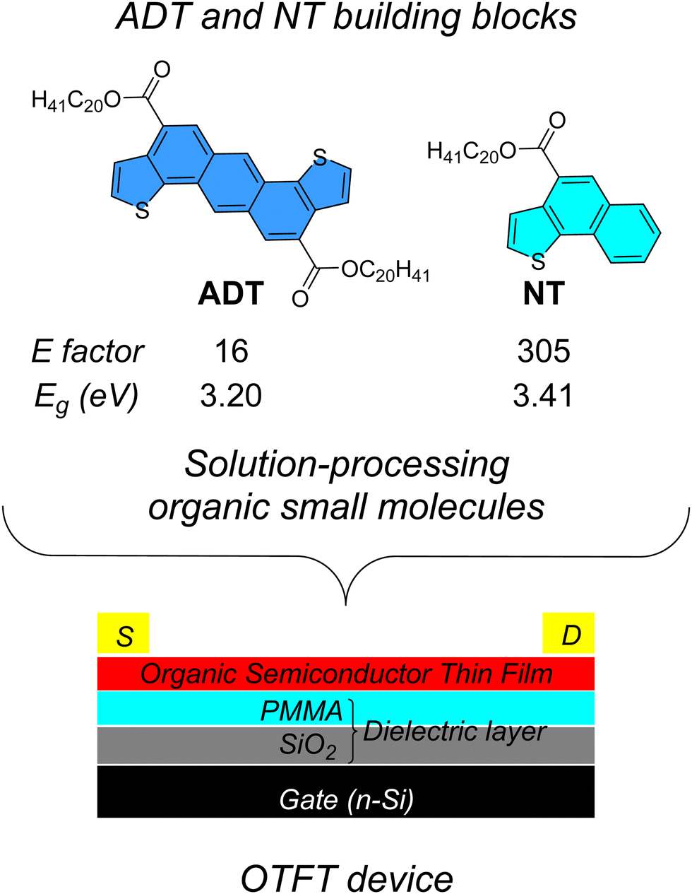 | ||
| Fig. 1 Molecular structures of ADT- and NT-based synthons and their implementation in solution-processable OTFT devices. | ||
Our design scheme for the synthesis of green, sustainable organic small molecule semiconductors relied on the following key points: (a) naphthothiophene (NT), possessing a single α-thiophene position, can act as an endcapping unit, whereas difunctional ADT can serve as the π-core; (b) the use of a BDT derivative for comparison of performance; (c) the exploitation of branched or linear alkyl chains, with different steric hindrance and packing effects, to exploit possible segregation and planarization effects of the organic materials in the solid-state.
Here, we report the synthesis and the evaluation of small molecule semiconductors (compounds 6–8) as low-cost organic and flexible OTFTs electronic devices. Compound 6 has been previously reported,34 but not evaluated in OTFTs. We characterized the electrical performances of the devices and we compared them with the morphology of the semiconductor films, studied through atomic force microscopy (AFM) measurements. Among the possible applications, we propose and effectively demonstrate the competitiveness of these materials as the key components of an organic phototransistor (OPT), capable of detecting low intensity light in a controlled way.
Results and discussion
1. Synthesis and characterization of the molecular organic semiconductors
The synthetic routes to the new semiconductors are shown in Fig. 2. The synthesis of compound 3, already reported,36,38 was substantially improved during this study, as reported in the ESI,† using the alkyl iodide 2 as alkylating agent, in the presence of potassium carbonate as base and tetrabutylammonium iodide (TBAI) as a phase transfer agent, resulting in an overall yield of 73%. The improvement in the yield resulted in an improvement of the corresponding E factor39 from 1836 to 16 (Fig. 1). The E factor, defined as the ratio of the mass of waste per mass of product, is probably the most widely used green metric to characterize organic synthesis. Our E factor calculations do not take into account the solvent of the reaction, which could be entirely recovered by distillation, and of the solvents used in the device preparation. The stannylation reaction of compound 3 to afford compound 4a was again further optimized (the new protocol is reported in the ESI†) and 4a was obtained with a yield of 94%.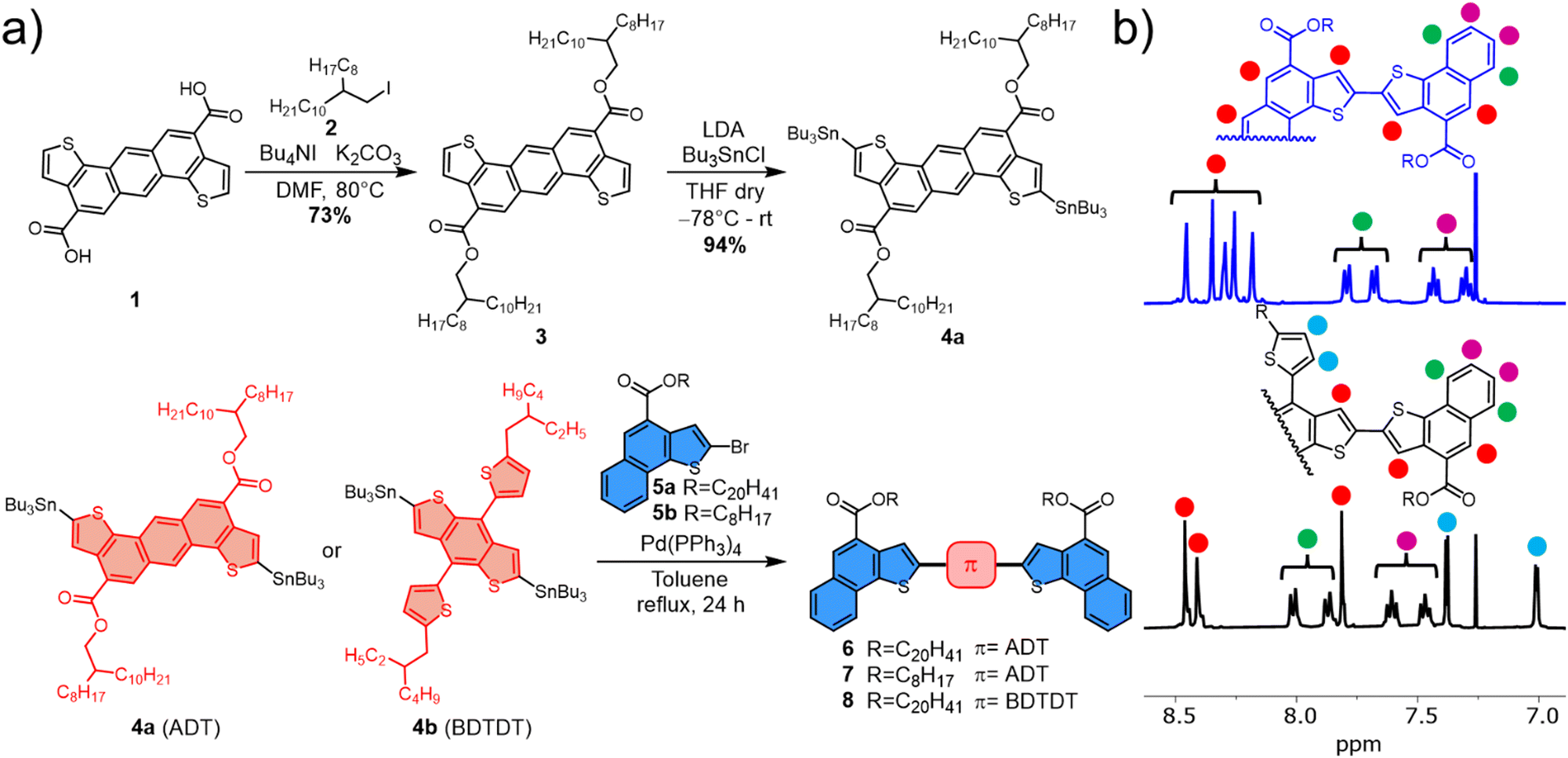 | ||
| Fig. 2 (a) Synthetic scheme of compounds 6–8. (b) Stacked spectra of compounds 6 (blue) and 8 (black) in CDCl3. | ||
As previously mentioned, we were interested in introducing both linear and branched alkyl chains within the conjugated backbone. The stannylation of the ADT analogue of 3 bearing linear octyl alkyl chains failed under all conditions attempted, presumably because of the marked reduction of solubility of the analogue in the optimal stannylation conditions of solvent and temperatures. The variability in introducing branched or linear alkyl chains was therefore addressed using either NT derivatives 5a and 5b. Subsequent Stille reactions with either 4a or 4b, using Pd(PPh3)4 as catalyst in toluene at reflux, afforded compounds 6–8, after purification by flash chromatography, in similar yields (around 70%). The chemical structures and purity of the new compounds were confirmed by 1H NMR, 13C NMR, bidimensional experiments (COSY and HSQC) and MALDI-TOF mass spectrometry (ESI†).
The comparison between the 1H NMR spectra (see Fig. 2 left) of compounds 6 (blue) and 8 (black) in their aromatic region revealed marked differences (>0.3 ppm) in the proton resonances for the two compounds. The doublet and triplet of terminal benzene rings in NT moieties in green and purple, respectively, are particularly affected. Such differences, given that the NT terminal units are the same in both 6 and 8, must be attributed to differences in the extent to which the differing central π-cores distribute π-charge through conjugation (see also below). The homologue 7, instead, in CDCl3 solution at room temperature, showed already the tendency to aggregate (See ESI†), demonstrating how the change from branched to linear alkyl chains had a marked effect on the possibility of the π-cores to stack, even in solution.
The photophysical properties in solution and film of compounds 6 and 8 are compared in Table 1.
| Compound | λ abs (nm, solution) | ε × 104 (M−1 cm−1) | λ em (nm) | QYb (%) | λ abs (nm, film) | E optg (eV, film) | HOMOd (eV) | LUMOd (eV) | λ em (nm, film) |
|---|---|---|---|---|---|---|---|---|---|
| a In CHCl3 (10−5 M). b Fluorescence quantum yield (CHCl3 solutions). c Obtained by casting of CHCl3 solutions (ca. 10−3 M) of the chromophores. d Obtained by cyclic voltammetry in solution. e Data taken from ref. 34. | |||||||||
| 6 | 444 | 4.49 | 524 | 3 | 471 | 2.31 | −5.03 | −2.81 | 766 |
| 8 | 417 | 4.47 | 490 | 8 | 421 | 2.29 | −5.22 | −2.97 | 627 |
In the case of compound 7, the absorption and emission spectra were superimposable to those of analogue 6. Both compounds exhibited strong absorption in the 250–500 nm region with a maximum extinction coefficient of around 4.5 × 10⁴ M−1 cm−1 at the λmax (444 nm and 417 nm, respectively). The absorption bands are broad for 6–8 testifying their flexible structures, induced by the aryl–aryl bonds, around which free rotation, cross-talking and conjugation between the differing chromophores are allowed (Fig. S1, ESI†). The photoluminescent spectra (PL) of compound 8 (Fig. S2, ESI†), similarly to 6 and 7, exhibits broad emission bands, typical of conjugated oligomers with substantial degrees of conformational freedom, with a PLQY of 8% (vs. 3% for 6). Compound 8 displays large Stokes shift in solution, measured as 73 nm (3570 cm−1) vs. 80 nm (3440 cm−1) for 6. In thin films substantially red-shifted profiles with respect to solution for all compounds could be observed. The optical bandgaps in film, estimated from the absorption edges (538 nm and 542 nm), are 2.31 eV and 2.29 eV respectively.
Compounds 6–8 have a shelf life exceeding one year in the solid state, when stored under ambient conditions in the dark. They exhibit good solubility (up to 90 mg mL−1) in common solvents (DCM, CHCl3, toluene and THF), enabling convenient device fabrication via solution processing.
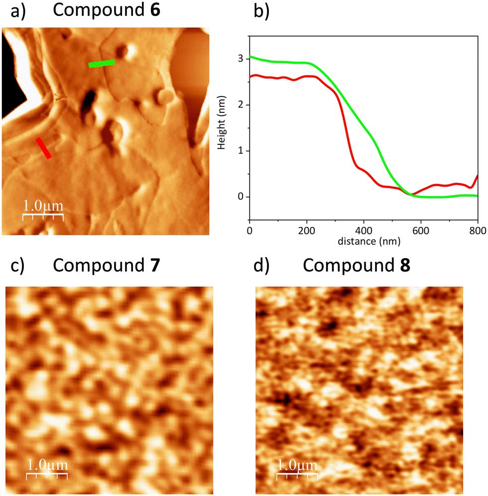 | ||
| Fig. 3 (a) AFM error signal 5 × 5 μm image of compound 6 OTFT device; (b) line profile acquired from topography image corresponding to Fig. 3a, reported in Fig. S3 (ESI†). The line colours correspond to the line reported in Fig. 4d; (c) and (d) AFM topography 5 × 5 μm image of compound 7 and 8 top surface OTFT device, respectively. | ||
The AFM analysis of compound 6 (in Fig. 3a is shown the error signal measurement, the corresponding topography image is reported in Fig. S4b, ESI†) reveals that the surface is rather flat. The film appears to be layered as an overlap of many sheets whose thickness is between 2.5 and 3 nm, as shown in Fig. 3b, where the height profiles measured in the topographic image are shown in correspondence with the coloured segments drawn in Fig. 3a. The measured thickness of the layers is compatible with the size of the central core of ADT of compound 6, about 2.8 nm.36
This suggests that the molecules are aligned with their central core oriented upright with respect to the underlying PMMA substrate.22Fig. 3c and d show 5 × 5 μm topographic AFM images of the surface of the films of compound 7 and 8, respectively. The film of compound 7 does not appear to have any large defects and there are no large holes or unevenness. The RMS roughness is 1.95 nm over the whole image data. The film of compound 8 does not show large defects as well, and in this case the relative roughness RMS calculated is 0.61 nm. However, unlike the film of compound 6, both compound 7 and 8 samples do not show a layered structure, suggesting a different alignment of the molecules in the film.
2. Organic thin film transistor
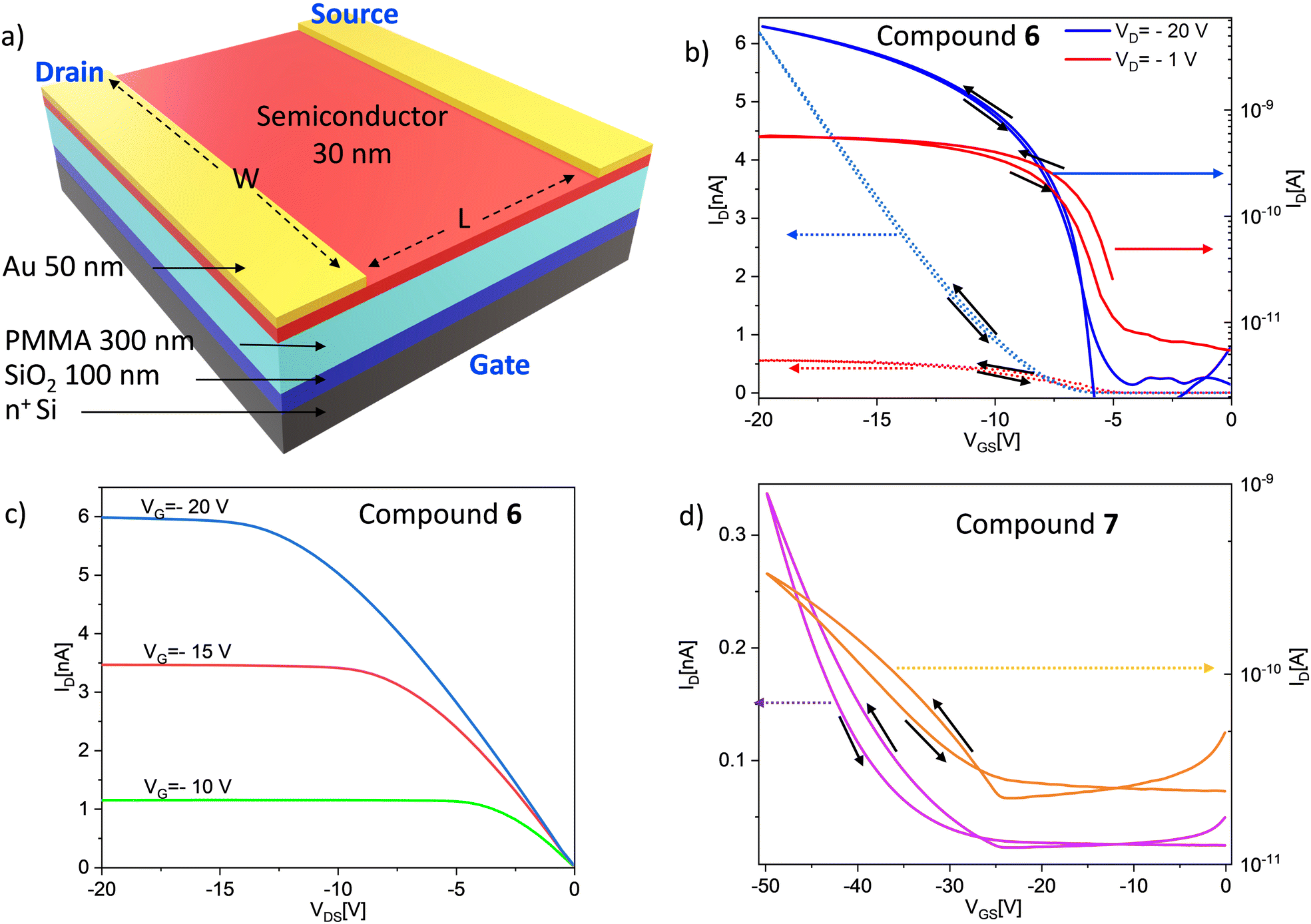 | ||
| Fig. 4 (a) Scheme of the OTFT fabricated with a staggered BGTC structure. (b) Up-down transfer characteristics of L = 100 μm device fabricated with compound 6 semiconductor materials in linear scale (dot lines, left scale) and in log scale (continuous lines, right scale). Red lines are measured in linear regime with applied VDS = −1 V, while blue lines are measured in saturation regime with VDS = −20 V. The black arrows indicate the direction (up or down) of I–V acquisition. (c) Output characteristics of the same OTFT reported in figure (a), for different values of VGS = −10 V, −15 V, −20 V, green, red, and blue curves respectively; (d) Up-down transfer characteristics of L = 50 μm device fabricated with compound 7 semiconductor materials in linear scale (violet line, left scale) and in log scale (orange line, right scale) for VDS = −30 V. The black arrows indicate the direction (up or down) of I–V acquisition. | ||
The above characteristics suggest an excellent quality of the semiconductor/dielectric interface and low defect density in the semiconductor layer. In Fig. 4d the up-down transfer characteristics, of compound 7 OTFT, L = 50 μm, are shown in linear (violet curve) and log scale (orange curve) for VDS = −30 V. The calculated field-effect mobility, threshold voltage and subthreshold slope are μFE = 8.3 × 10⁻⁶ cm2 V−1 s−1, and VTH = −27.6 V, SS = 8 V dec−1, respectively, with a corresponding on/off ratio ranging between 10 and 100. These data evidence that the compound 7 semiconductor has poorer electrical characteristics, compared to compound 6. Furthermore, for this compound the hysteresis in the IDvs. VGS curve shows an instability of the OTFT, probably related to water/oxygen absorption in the semiconductor film. Unlike the compounds 6 and 7, the fabricated compound 8 OTFTs do not show the typical electrical characteristics of a transistor. Indeed, the measured drain current is very low and shows no modulation with the gate voltage. The worse electrical characteristics and worse performances of the compound 7 and 8 OTFTs can be related to the different film structures (molecule alignment) evidenced by the AFM analysis. In the case of compounds 6, although our devices are not high field-effect mobility transistors, their electrical characteristics and performances are superior to many other organic semiconductor systems reported in the literature, even though the device structure was mainly intended for testing of semiconductor characteristics not to optimize the device parameters. On the other hand, other characteristics of this semiconductor, such as the optoelectronic properties, can be exploited for device application, as shown in the next section.
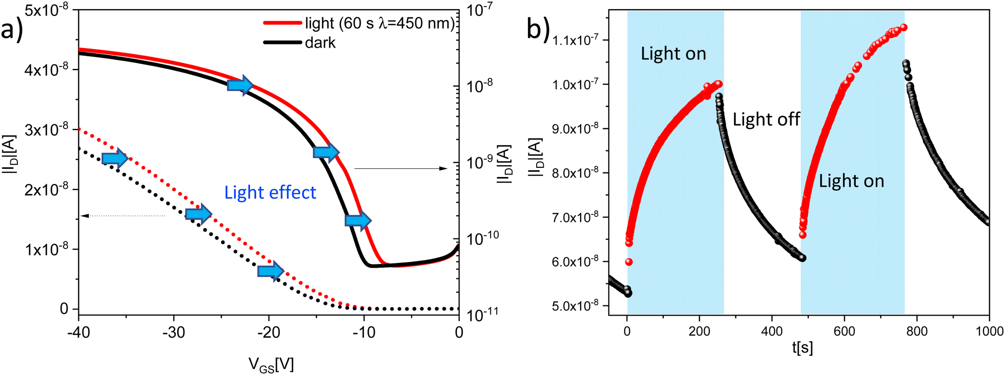 | ||
| Fig. 5 (a) Transfer characteristics of a L = 100 μm OTFT devices acquired in dark conditions (blue curves) and after 60 s of 450 nm illumination (red curves) for VDS = −20 V. The continuous lines refer to right log scale while the dotted lines refer to left linear scale. The blue arrows indicate the rightward threshold shift of the curves as a consequence of the illumination; (b) transient drain current IDvs. time for VDS = −20 V and VGS = −15 V. The blue squares on the graphs represent the time lamps when the device is illuminated. | ||
Conclusions
We have extended our synthetic methodology of green, sustainable organic small molecule semiconductors by realizing and characterizing three substrates, in which NTs acted as endcapping units, and ADT BDT moieties served as the π-core, and in which variability in terms of branched or linear alkyl chains was introduced.These small molecule semiconductors can be effectively used as the active materials in low-cost organic and flexible OTFTs electronic devices. We have obtained good electrical characteristics for materials composed of the ADT scaffold. For compound 6, as evidenced by the AFM measurements, the oligomers manage to organize themselves forming a stratified semiconductor film. The small molecules self-arrange in such a way that the central core, formed by the ADT, is packed with its longest axis vertically with respect to the plane of the substrate, in the so-called chain-on configuration, π-stacking in the plane, that is the most favourable molecular packing configuration for carrier transport in organic semiconductors. The compound 7 cannot orient itself as well as 6, leading to inferior electrical characteristics both in terms of field effect mobility and in terms of stability. The same situation occurs for compound 8, which contains the BDTDT as central scaffold of the polymer, that does not show good transistor electrical characteristics. Finally, we have demonstrated that compound 6 can be efficiently used also as the active layer of an organic phototransistor, with responsivity values of 3.5 A W−1, matching currently available commercial detectors. These optoelectronic properties, combined with the possibility of a green and low-cost synthesis make these devices attractive for competitive and innovative applications.
Author contributions
Conceptualization, D. P., L. M., M. R. and L. B.; methodology, A. N. and M. S.; formal analysis, A. N. and M. S.; writing – original draft preparation M. S., A. N. and D.P.; writing – review and editing, M. R. and D. P.; supervision, M. R. and D. P.; funding acquisition, D. P., L. M. and L. B.Conflicts of interest
There are no conflicts to declare.Acknowledgements
This work was supported by MIUR under 2017YXX8AZ PRIN grant. A. N. and D. P. acknowledge support from the Ministero dell’Università e della Ricerca (MUR) and the University of Pavia through the program “Dipartimenti di Eccellenza 2023–2027”. We thank Chiara Botta (CNR Milan), for help with the emission and quantum yields determination.References
- K. Myny, Nat. Electron., 2018, 1, 30–39 CrossRef CAS.
- B. Crone, A. Dodabalapur, Y. Y. Lin, R. W. Filas, Z. Bao, A. LaDuca, R. Sarpeshkar, H. E. Katz and W. Li, Nature, 2000, 403, 521–523 CrossRef CAS PubMed.
- M. R. Niazi, R. Li, E. Q. Li, A. R. Kirmani, M. Abdelsamie, Q. Wang, W. Pan, M. M. Payne, J. E. Anthony, D.-M. Smilgies, S. T. Thoroddsen, E. P. Giannelis and A. Amassian, Nat. Commun., 2015, 6, 8598 CrossRef CAS PubMed.
- M. R. Cavallari, L. M. Pastrana, C. D. Flecha Sosa, A. M. Rodriguez Marquina, J. E. Eirez Izquierdo, F. Josepetti Fonseca, C. Alexandre de Amorim, L. G. Paterno and I. Kymissis, Materials, 2021, 14, 3 CrossRef CAS PubMed.
- O. A. Melville, B. H. Lessard and T. P. Bender, ACS Appl. Mater. Interfaces, 2015, 7, 13105–13118 CrossRef CAS PubMed.
- C. R. Newman, C. D. Frisbie, D. A. da Silva Filho, J.-L. Bredas, P. C. Ewbank and K. R. Mann, Chem. Mater., 2004, 16, 4436–4451 CrossRef CAS.
- M. E. Roberts, A. N. Sokolov and Z. Bao, J. Mater. Chem., 2009, 19, 3351–3363 RSC.
- Y. Wen and Y. Liu, Adv. Mater., 2010, 22, 1331–1345 CrossRef CAS PubMed.
- S. A. Di Benedetto, A. Facchetti, M. A. Ratner and T. J. Marks, Adv. Mater., 2009, 21, 1407–1433 CrossRef CAS.
- Y. Wen, Y. Liu, Y. Guo, G. Yu and W. Hu, Chem. Rev., 2011, 111, 3358–3406 CrossRef CAS PubMed.
- M. M. Payne, S. R. Parkin, J. E. Anthony, C.-C. Kuo and T. N. Jackson, J. Am. Chem. Soc., 2005, 127, 4986–4987 CrossRef CAS PubMed.
- W.-L. Liau, T.-H. Lee, J.-T. Chen and C.-S. Hsu, J. Mater. Chem. C, 2016, 4, 2284–2288 RSC.
- Q. Meng, L. Jiang, Z. Wei, C. Wang, H. Zhao, H. Li, W. Xua and W. Hu, J. Mater. Chem., 2010, 20, 10931–10935 RSC.
- M.-C. Chen, C. Kim, S.-Y. Chen, Y.-J. Chiang, M.-C. Chung, A. Facchetti and T. J. Marks, J. Mater. Chem., 2008, 18, 1029–1036 RSC.
- V. Coropceanu, J. Cornil, D. A. da Silva Filho, Y. Olivier, R. Silbey and J.-L. Brédas, Chem. Rev., 2007, 107, 926–952 CrossRef CAS PubMed.
- J. Hou, O. Inganäs, R. H. Friend and F. Gao, Nat. Mater., 2018, 17, 119–128 CrossRef CAS PubMed.
- J. X. Chen, Y. F. Xiao, K. Wang, D. Sun, X. C. Fan, X. Zhang, M. Zhang, Y. Z. Shi, J. Yu and F. X.Geng, Angew. Chem., Int. Ed., 2021, 133, 2508–2514 CrossRef.
- K. Takimiya, S. Shinamura, I. Osaka and E. Miyazaki, Adv. Mater., 2011, 23, 4347–4370 CrossRef CAS PubMed.
- A. Velusamy, S. N. Afraj, S. Yau, C.-L. Liu, Y. Ezhumalai, P. Kumaresan and M.-C. Chen, J. Chin. Chem. Soc., 2022, 69, 1253–1275 CrossRef CAS.
- C. Kim, P.-Y. Huang, J.-W. Jhuang, M.-C. Chen, J.-C. Ho, T.-S. Hu, J.-Y. Yan, L.-H. Chen, G.-H. Lee, A. Facchetti and T. J. Marks, Org. Electron., 2010, 11, 1363–1375 CrossRef CAS.
- M. Sobhani, A. Villinger, P. Ehlers and P. Langer, J. Org. Chem., 2022, 87, 4560–4568 CrossRef CAS PubMed.
- D. S. Baranov, A. A. Popov, D. A. Nevostruev, A. A. Dmitriev, Y. V. Gatilov and E. S. Kobeleva, J. Org. Chem., 2021, 86, 11361–11369 CrossRef CAS PubMed.
- C. C. Anghel, I. Stroia, A. Pop, A. Bende, I. Grosu, N. D. Hădade and J. Roncali, RSC Adv., 2021, 11, 9894–9900 RSC.
- L. Yu, G. Portale and N. Stingelin, J. Mater. Chem. C, 2021, 9, 10547–10556 RSC.
- H. Yao, L. Ye, H. Zhang, S. Li, S. Zhang and J. Hou, Chem. Rev., 2016, 116, 7397–7457 CrossRef CAS PubMed.
- M. Mamada, T. Minamiki, H. Katagiri and S. Tokito, Org. Lett., 2012, 14, 4062–4065 CrossRef CAS PubMed.
- B. Tylleman, C. M. L. Vande Velde, J.-Y. Balandier, S. Stas, S. Sergeyev and Y. H. Geerts, Org. Lett., 2011, 13, 5208–5211 CrossRef CAS PubMed.
- G. Albano, A. Punzi, M. A. M. Capozzi and G. M. Farinola, Green Chem., 2022, 24, 1809–1894 RSC.
- A. Baccalini, G. Faita, G. Zanoni and D. Maiti, Chem. – Eur. J., 2020, 26, 9749–9783 CrossRef CAS PubMed.
- A. Nitti, R. Po, G. Bianchi and D. Pasini, Molecules, 2017, 22, 21 CrossRef PubMed.
- L. Levi and T. J. J. Müller, Chem. Soc. Rev., 2016, 45, 2825–2846 RSC.
- F. Corsini, A. Nitti, E. Tatsi, G. Mattioli, C. Botta, D. Pasini and G. Griffini, Adv. Opt. Mater., 2021, 9, 2100182 CrossRef CAS.
- A. Nitti, P. Osw, M. N. Abdullah, A. Galbiati and D. Pasini, Synlett, 2018, 2577–2581 CAS.
- A. Nitti, G. Bianchi, R. Po and D. Pasini, Synthesis, 2019, 677–682 CrossRef CAS.
- P. Osw, A. Nitti, M. N. Abdullah, S. I. Etkind, J. Mwaura, A. Galbiati and D. Pasini, Polymers, 2020, 12, 720 CrossRef CAS PubMed.
- A. Nitti, G. Forti, G. Bianchi, C. Botta, F. Tinti, M. Gazzano, N. Camaioni, R. Po and D. Pasini, J. Mater. Chem. C, 2021, 9, 9302–9308 RSC.
- A. Nitti, P. Osw, G. Calcagno, C. Botta, S. I. Etkind, G. Bianchi, R. Po, T. M. Swager and D. Pasini, Org. Lett., 2020, 22, 3263–3267 CrossRef CAS PubMed.
- G. Bianchi, C. Carbonera, L. Ciammaruchi, N. Camaioni, N. Negarville, F. Tinti, G. Forti, A. Nitti, D. Pasini, A. Facchetti, R. M. Pankow, T. J. Marks and R. Po, Sol. RRL, 2022, 6, 2200643 CrossRef CAS.
- R. A. Sheldon, Green Chem., 2007, 9, 1273–1283 RSC.
- V. R. Rajeev, S. Pillai, J. M. Nunzi and K. N. N. Unni, Macromol. Mater. Eng., 2022, 307, 2100716 CrossRef.
- M. Rapisarda, S. Calvi, M. Barra, F. Chiarella, F. Di Capua, A. Cassinese, A. Aloisio and L. Mariucci, Org. Electron., 2018, 57, 226–231 CrossRef CAS.
- C. Ceriani, M. Scagliotti, T. Losi, A. Luzio, S. Mattiello, M. Sassi, N. Pianta, M. Rapisarda, L. Mariucci, M. Caironi and L. Beverina, Adv. Electron. Mater., 2023, 9, 2201160 CrossRef CAS.
- J. W. Park, B. H. Kang and H. J. Kim, Adv. Funct. Mater., 2020, 30, 1904632 CrossRef CAS.
- F. A. Viola, J. Barsotti, F. Melloni, G. Lanzani, Y.-H. Kim, V. Mattoli and M. Caironi, Nat. Commun., 2021, 12, 5842 CrossRef CAS PubMed.
- O. Vazquez-Mena, L. Gross, S. Xie, L. G. Villanueva and J. Brugger, Microelectron. Eng., 2015, 132, 236–254 CrossRef CAS.
- M. Rapisarda, A. Valletta, A. Daami, S. Jacob, M. Benwadih, R. Coppard, G. Fortunato and L. Mariucci, Org. Electron., 2012, 13, 2017–2027 CrossRef CAS.
- A. Facchetti, Mater. Today, 2007, 10, 28–37 CrossRef CAS.
- J. Zaumseil and H. Sirringhaus, Chem. Rev., 2007, 107, 1296–1323 CrossRef CAS PubMed.
- M. Rapisarda, D. Simeone, G. Fortunato, A. Valletta and L. Mariucci, Org. Electron., 2011, 12, 119–124 CrossRef CAS.
- D. Simeone, S. Cipolloni, L. Mariucci, M. Rapisarda, A. Minotti, A. Pecora, M. Cuscunà, L. Maiolo and G. Fortunato, Thin Solid Films, 2009, 517, 6283–6286 CrossRef CAS.
- S. Calvi, M. Rapisarda, A. Valletta, M. Scagliotti, S. De Rosa, L. Tortora, P. Branchini and L. Mariucci, Org. Electron., 2022, 102, 106452 CrossRef CAS.
- S. Calvi, L. Basiricò, S. M. Carturan, I. Fratelli, A. Valletta, A. Aloisio, S. De Rosa, F. Pino, M. Campajola, A. Ciavatti, L. Tortora, M. Rapisarda, S. Moretto, M. Verdi, S. Bertoldo, O. Cesarini, P. Di Meo, M. Chiari, F. Tommasino, E. Sarnelli, L. Mariucci, P. Branchini, A. Quaranta and B. Fraboni, npj Flexible Electron., 2023, 7, 5 CrossRef CAS.
- K.-J. Baeg, M. Binda, D. Natali, M. Caironi and Y.-Y. Noh, Adv. Mater., 2013, 25, 4267–4295 CrossRef CAS PubMed.
- B. Lucas, T. Trigaud and C. Videlot-Ackermann, Polym. Int., 2012, 61, 374–389 CrossRef CAS.
- M. Scagliotti, A. Valletta, S. Calvi, L. Mariucci and M. Rapisarda, IEEE Sens. Lett., 2023, 7, 1–4 Search PubMed.
- H. Ren, J.-D. Chen, Y.-Q. Li and J.-X. Tang, Adv. Sci., 2021, 8, 2002418 CrossRef CAS PubMed.
Footnotes |
| † Electronic supplementary information (ESI) available. See DOI: https://doi.org/10.1039/d3ma00552f |
| ‡ These authors contributed equally. |
| This journal is © The Royal Society of Chemistry 2023 |