DOI:
10.1039/D3MA00166K
(Paper)
Mater. Adv., 2023,
4, 3246-3256
First principle insights and experimental investigations of the electronic and optical properties of CuInS2 single crystals
Received
11th April 2023
, Accepted 26th June 2023
First published on 10th July 2023
Abstract
The function of the Perdew–Burke–Ernzerhof (PBE) approach is employed in density functional calculations to investigate copper indium disulfide (CuInS2) single crystals. The utilization of the generalized gradient approximation (GGA + U) method enhances the fluency and accuracy of the computation. This enabled the evaluation of band structure and density of states (DOS), including optical features like conductivity, reflectivity, refractive index, loss function, dielectric function, and absorption coefficient. The density of states (DOS) revealed that the valence bands at 0.8 eV are mostly a result of hybridisation between the In(5p) and S(3p) levels with slight input from Cu(3d). The CuInS2 single crystals are synthesised using a chemical vapour transport technique. Optical parameters such as optical density, skin depth, Urbach's parameters, refractive index, extinction coefficient, and dielectric constant are evaluated. The optical direct and indirect bandgap values are found as 1.60 eV and 1.51 eV, respectively. The band tailing or Urbach energy is calculated as 0.056 eV, allowing an accurate indirect bandgap of 1.454 eV to be predicted. The wavelength corresponding to the intersection of the real and imaginary dielectric functions is 819 nm, closer to the absorption band edge (797 nm).
1. Introduction
In the ever-expanding family of three-dimensional materials, for photonic applications, notably in the field of flexible optoelectronics, those having semiconducting properties of transition metal dichalcogenides (TMDCs) are of particular interest in recent advances. The TMDCs are of great attention to researchers due to the variety of their structural and electrical characteristics, such as thermoelectric effect,1,2 thermal study,3–6 superconductivity,7,8 optical study,9,10 photovoltaic devices,11,12 biological applications,13–16etc. Among the TMDCs, chalcopyrite-type semiconducting materials are being sought for their equally significant and environmentally benign nature, as well as prospective applications in a variety of optical instruments in the visible and near-infrared regions. The chalcopyrite CuInS2 (CIS) single crystals belonging to the I–III–IV2 group have increased consideration due to their great chemical stability and distinctive optoelectronic features. They include varying bandgap values with minor stoichiometric variation and an absorption coefficient ideal for optoelectronic devices over the entire range of the electromagnetic spectrum. Furthermore, electronics, opto-electronics, microelectronics, communications, and energy generation are just a few of the many areas where CIS semiconducting materials find widespread use in today's advanced technology and industry.17–19 The CIS single crystals are an excellent candidate for solar-energy conversion because of their significant absorption coefficient (∼105 cm−1) and direct optical energy bandgap (1.36 eV to 1.54 eV).20,21
The electronic and optical properties of single crystals depend on their structure, surface, chemical composition, purity, and mechanical stability. It is crucial to achieve the controlled synthesis of CIS single crystals of large domains and sizes for such a purpose. This is found to be possible by an efficient and affordable chemical vapour transport (CVT) technique. The CVT has shown promise in the synthesis of superior crystals. Several tactics have been suggested to accelerate the development rate of single crystals. Due to the finite size, no crystal could be perfect because a perfect one would extend indefinitely in all directions. The features of a single crystal grown by CVT are affected by both vacuum and growth conditions, which include residual pressure, content, spatial arrangement, and surface topography. It has been the subject of intriguing research in the past and is currently used in optoelectronic devices.
Prior research publications on CIS often focused on investigating electronic and optical aspects.22–25 Despite all this research, several electronic and optical characteristics, such as electronic band structure, optical conductivity, reflectivity, refractive index, loss function, dielectric function, and absorption coefficient, are not done utilising density functional theory (DFT) via the first principles approach. Additionally, a number of optical characteristics, including optical density, skin depth, Urbach's parameters, refractive index, extinction coefficient, and dielectric constant, have not been discussed in relation to previous studies of CIS. As a result, our objective for this work is to enhance existing estimates, investigations, and studies of electronic and optical features of CIS single crystals that have not previously been studied in the literature. Also, the correlation between the electronic and optical parameters estimated from DFT+U and experimental investigation is discussed in detail.
2. First principle calculation
The generalised-gradient approximation (GGA + U, U = 2.5 eV additional energy optimized for Cu transition metal) method with the function of the Perdew–Burke–Ernzerhof (PBE) approach is utilised in the Quantum Espresso simulation programme for the density functional computation method.26,27 The GGA–PBE function estimates cut-off energy of 500 eV. A huge 12 × 12 × 12 grid is used for high symmetric band structure calculation. The energy for ionic relaxation is set to 500 eV, while electronic self-consistent relaxation is set to 0.02 eV A−1, and both are utilised as convergence criteria for the single crystal unit cell grid.
2.1. Crystal structure
CIS crystallises in the tetragonal Ī42d space group, taking on the crystal structure of chalcopyrite (Fig. 1). CuS4 tetrahedra are formed when Cu1+ ions are joined to four S2− ions. These tetrahedra share corners with four CuS4 tetrahedra and eight equivalent InS4 tetrahedra. The bond lengths between Cu and S atoms are uniform and measured as 2.31 Å. Conversely, the In3+ ions form InS4 tetrahedra by bonding with four equivalent S2− atoms. These tetrahedra share corners with four equivalent InS4 tetrahedra and eight equivalent CuS4 tetrahedra. The bond lengths between In and S atoms are consistent and measured as 2.49 Å. Additionally, four S2− ions are bonded to two equivalent Cu1+ atoms and two equivalent In3+ atoms forming CuInS2 tetrahedra that share corners.
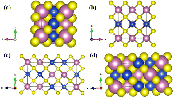 |
| | Fig. 1 (a, b, c, d) Crystal structure of CuInS2; the pink (large), blue (middle), and yellow (small) balls represent In, Cu, and S atoms, respectively. | |
2.2. Electronic band structure
Fig. 2 represents the band structure and density of states (DOS) analysis for a single crystal of CIS (copper indium disulfide). To capture the electronic behaviour accurately, the DFT+U strategy incorporates a Hubbard term with a value of U = 2.5 eV specifically for the Cu(3d) atoms. From Fig. 2(a), it becomes evident that the spin orbital coupling (SOC) acts as a relativistic minor interaction, influencing the Cu (3d) spin within the U = 2.5 potential. Remarkably, the alignment of Cu and S electrons in each other's directions results in negligible changes in the magnetic moments. The lower conduction bands depicted in Fig. 2(a) primarily originate from the In(5s), S(3s), and S(3p) states. On the other hand, the highest valence bands are predominantly determined by the Cu(3d) and S(3p) states, with some contributions from the In(5p) states. At an energy level of 0.8 eV, the valence bands mainly result from the hybridization between the In(5p) and S(3p) levels, with a minor contribution from Cu(3d). Additionally, Fig. 2(b) depicts that the In(5s) state occupies a significantly distant energy range spanning from +5 to −5 eV.
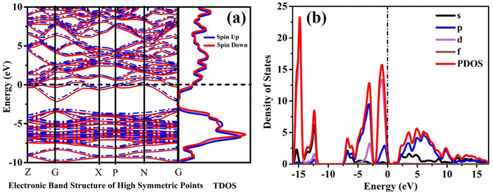 |
| | Fig. 2 The (a) electronic band structure, and (b) projection DOS. | |
2.3. Optical properties
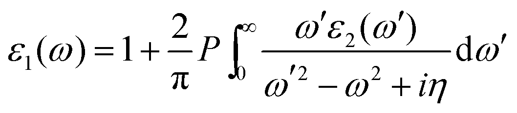
The dielectric function, which varies with frequency, ε(ω) can be utilised to quantify the optical characteristics of a wide range of materials.28 In terms of the most important aspect of optical properties, it is a challenging quantity to deal with. The dielectric function, ε(ω) is represented as,
While considering optical characteristics of different materials, photovoltaics is an example. The PBE–GGA theoretical notations allow us to estimate a crucial aspect of the optical parameters, namely ε2(ω).29
| | 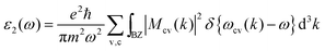 | (2) |
Eqn (2) represents the integral of the initial Brillouin zone. Furthermore,
| | | Mcv(k) = 〈uck|e·∇|uvk〉 | (3) |
where
e denotes the electric field and stands for the potential vector. Direct valence and conduction band transitions are denoted by the symbols
uvk(
r) and
ħωcv, respectively. The transition energy (=
Eck −
Evk) is represented by
ħωcv.
Using the Kramers–Kronig relation,30 the real portion ε1(ω) in eqn (1) may be deduced from the imaginary part ε2(ω). Mathematically,
| |  | (4) |
where
P denotes the integral's principal value, and
g represents an infinitesimal number.
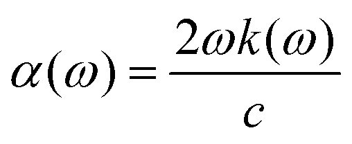
Computing the absorption coefficient employing dielectric functions provides a scientific insight into photovoltaics.31 The absorption coefficient quantifies the amount of a particular wavelength's (or energy's) light that may pass through a substance before being absorbed.32 Absorption curves in semiconductors are generated by a number of inter-band transitions. They can also be assessed throughout the entire band gap region that allows direct band transitions.
The optical absorption coefficient (α) may be estimated using mathematical formula,
| |  | (5) |
The extinction coefficient, denoted as k(ω), relates to dielectric terms that reveal further information on optical properties and computational factors.
The investigation of optical properties contributes to an understanding of the electronic structure.33 The optical characteristics, complex conductivity σ(ω), reflectivity, refractive index, and absorption coefficient are determined. Gaussian smearing with a value of 0.5 eV is employed for all computations.
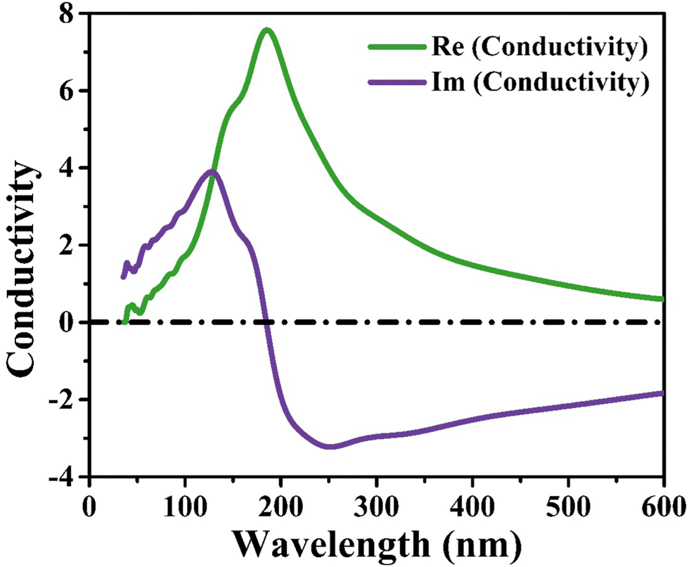
Conductivity.
The photoconductivity σ(ω) of a single crystal is directly connected to its energy band structure.34 Photoconductivity begins with photon energy of 130 nm, Fig. 3. This indicates that the material has a bandgap of around 0.8 nm. Interestingly, for photon energies below 50 nm, an intriguing characteristic emerges - the real component of conductivity becomes completely suppressed, effectively reaching zero. This suggests a unique behaviour in this energy range. However, as the material absorbs photons, a remarkable outcome ensues - the photoconductivity of the material, and consequently its electronic conductivity, experiences a significant boost, signifying a tangible increase in conductivity for CIS.
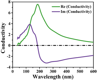 |
| | Fig. 3 The optical conductivity spectra. | |
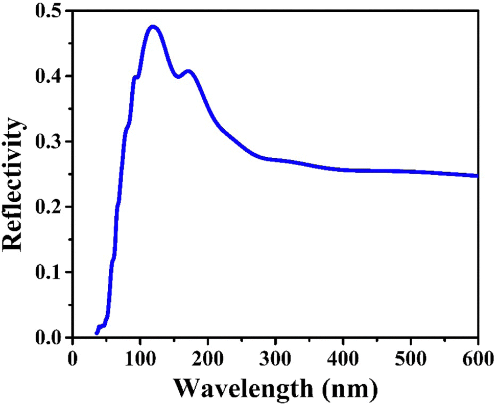
Reflectivity.
The reflectivity of a single crystal is represented by R(ω) = [(n − 1)2 + k2]/[(n + 1)2 + k2] in terms of n1 = 1 and n2 = n+ ik.35 This equation accounts for both the real (n) and imaginary (k) components of the refractive index, capturing the interaction of light with the crystal. To visualize the reflectivity behaviour, Fig. 4 illustrates the reflectivity spectrum specific to CIS. Upon analysing the spectrum, a notable observation emerges - regions characterized by low energy levels exhibit a remarkably high reflectivity. This distinctive characteristic suggests the presence of robust conductance within those particular energy ranges. In other words, the crystal exhibits enhanced reflectivity, signifying its ability to efficiently transmit and reflect light within those low-energy ranges, ultimately indicating strong conductive properties.
 |
| | Fig. 4 The reflectivity spectrum. | |
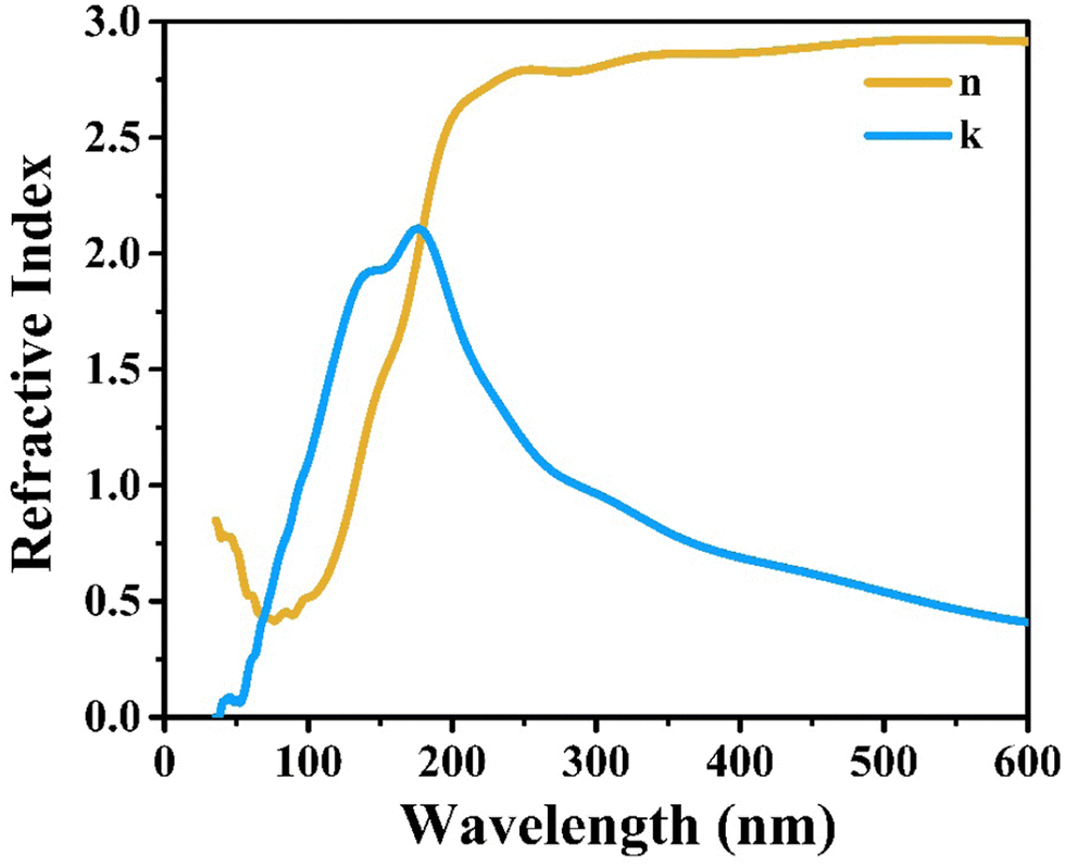
Refractive index.
In order to estimate the n and k values of refractive index and extinction coefficient, respectively, n2 − k2 = ε1, and 2nk = ε2 formulae are utilised.36Fig. 5 depicts the refractive index (n0) as the static refractive index. The plot shows that the refractive index experiences a peak at a wavelength of 240 nm. Concurrently, the extinction coefficient reaches its maximum value at 190 nm before rapidly decreasing beyond that point. These observations provide valuable insights into the optical behaviour of the material at different wavelengths, highlighting significant variations in the refractive index and extinction coefficient across the electromagnetic spectrum.
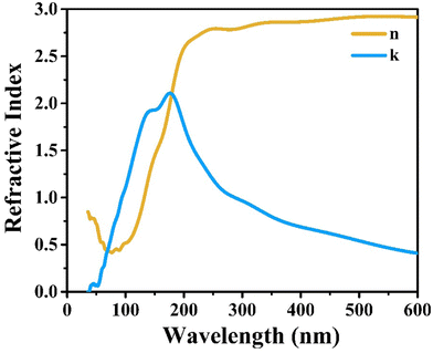 |
| | Fig. 5 The refractive index spectra. | |
Absorption coefficient.
The dielectric function and absorption coefficient are determined from α(ω) = ωε2(ω)/ne, and the absorption coefficient curve is exhibited in Fig. 6. Two notable absorption peaks appear at 50 nm and 140 nm in wavelength and are attributed to an interband transition between the Cu(3d) state in the conduction band and In(3p) level in the valence band. These transitions contribute significantly to the overall absorption behaviour of the CIS single crystal.
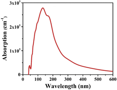 |
| | Fig. 6 The absorption spectrum. | |
Interestingly, the CIS single crystal is optically transparent for photon energy corresponding to wavelengths less than 40 nm and greater than 70 nm. The absorption coefficient increases from 70 nm wavelength to 140 nm wavelength to the highest peak achieving a maximum value of 2.7 × 105 cm−1, and subsequently drops with increasing photon energy until zero at 2.1 × 105 cm−1. These detailed observations provide valuable insights into the optical properties of the CIS crystal and its behaviour across a wide range of photon energies and corresponding wavelengths.
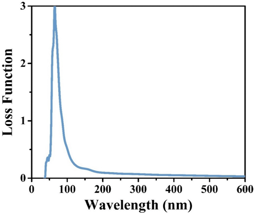
Loss function.
In the energy range of 0–600 nm, the loss function of CIS is estimated and exhibited in Fig. 7. The transmission of electrons through a material is characterised by its loss function, which provides a measure of the energy dissipated by each electron. Additionally, the loss function peak observed at 75 nm wavelength aligns with the trailing edges of the reflection spectrum. When considering a single Cu–In–S system, the intraband transition of the Cu(3d), In(3d), and S(3p) states within the conduction band plays a crucial role. Notably, the S(3p) state emerges as a prominent factor contributing to the peaks observed in the loss-function spectrum. This occurrence can be attributed to the predicted bandgap (0.8 eV), which falls short of the observed value (1.1 eV) specifically at the 75 nm wavelength. In relation to Fig. 6, the absorption spectrum of CIS, the absorption zone is fairly broad, as depicted, and the primary absorption section is located in the UV range. With the Cu–In–S system, the intraband transition between the Cu(3d), In(3d), and S(3p) states in the conduction band causes more absorption to be seen below the absorption edge in the visible area. This phenomenon arises due to the enhanced prominence of the S(3p) state within the conduction band, which further contributes to the absorption behaviour observed in the visible range.
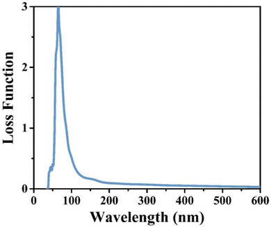 |
| | Fig. 7 The loss function spectrum. | |
Dielectric function.
Fig. 8 illustrates the imaginary dielectric function that represents the continuum of optical properties of the CIS single crystal. In the optical absorption spectrum, the primary peak is situated at 195 nm wavelength. The peak at 195 nm wavelength is caused by an electronic transition between the valence band of the Cu(3d) state and conduction band of the In(3d) state signifying a notable contribution in absorption behaviour.
 |
| | Fig. 8 Real and imaginary dielectric function curves. | |
The faint signal of Re(epsilon) at 132 nm is attributable to a transition in valence bands between the Cu(3d) and S(2p) states. The Im(epsilon) primary peak at 195 nm wavelength is caused by transition between In(3d) and S(2p) states. The plot at low wavelength (140 nm) is caused by the electronic intraband transition between Cu(3d) and In(3d) states in the conduction band, where the change in position is attributed to the S(2p) purity band's localised degree. In the high-wavelength region, these results show that the diverse Cu–In high energy region and In–S configurations mostly impact the optical characteristics in the low energy region. These detailed observations shed light on the complex interplay between different electronic states and their role in shaping the optical properties of the CIS single crystal.
3. Experimental
The CIS single crystals are grown by the CVT technique incorporating a transporting agent (iodine). A quartz ampoule with calibrated dimensions is filled with pure copper (∼99.5%, Alfa Aesar, USA), indium (∼99.99%, Sigma Aldrich, USA) and sulfur (∼99.99%, Oxford Laboratory, India) powders in stoichiometric proportion and iodine (2 mg cc−1) is taken in a narrow capillary to act as a transporting agent. The ampoule is sealed under vacuum of 10−5 torr pressure. This ampoule is placed into a calibrated dual-zone furnace for charge preparation for four days. The prepared charge is maintained in the furnace once more under the required conditions to produce single crystals of CIS. After ten days, this procedure produced shining black, thin flaky crystals of CIS.37
4. Results and discussion
4.1. Optical absorption
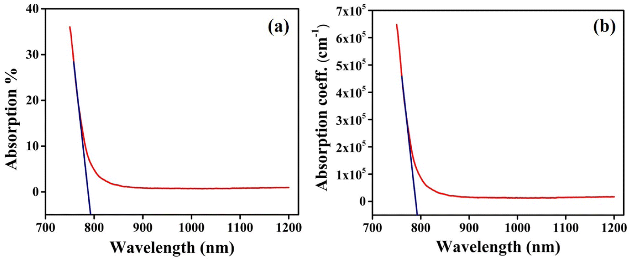
Optical properties of as-grown crystals depend on the preparation technique, conditions, surface morphology, and interaction with the surroundings. The lower energy region correlates to the atomic vibrations, whereas the higher energy region may be used to deduce information about the electronic states present in any semiconducting material through the analysis of spectral behaviour of its absorption coefficient.38 The optical absorption spectrum of the CIS single crystal is measured in the range of spectral wavelengths 700 to 1200 nm as depicted in Fig. 9. The absorption coefficient (α) values are in the order of ∼105 cm−1, confirming the ability of employing CIS single crystal for energy conversion. Extending the steep part of the absorption curve onto the photon energy intercepts a given point giving the absorption edge. The intersection point specifies a 1.55 eV value for the edge of the optical band at 797 nm.
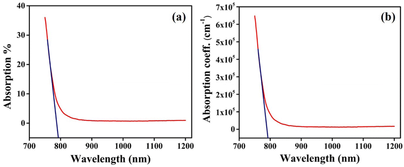 |
| | Fig. 9 The CIS (a) optical absorption %, and (b) absorption coefficient variation with incident wavelength. | |
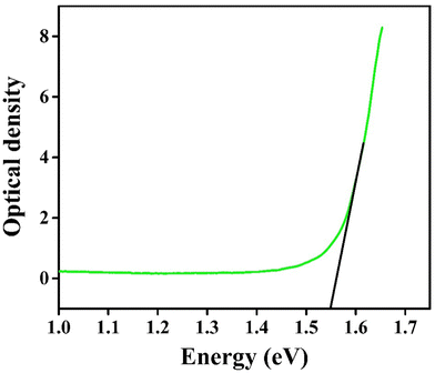
Furthermore, optical density depends on the concentration of the sample and its thickness. It is expressed by the product of the absorption coefficient (α) and thickness of the medium.39 The optical density variation with incident photon energy is shown in Fig. 10. It exhibits a similar nature of optical band edge value corresponding to 1.55 eV (Fig. 9).
 |
| | Fig. 10 The optical density spectrum. | |
4.2. Skin depth (δ)
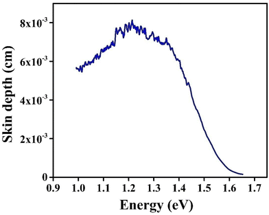
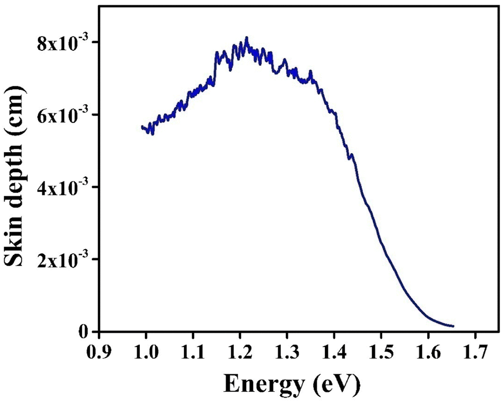
The energy from the incident beam that remains on the sample surface of a semiconductor in spectral areas of strong absorption is energy that is reflected at the surface. Hence, certain distinctive and significant factors, such as the skin depth and optical conductivity, are related to absorption of photons within the crystal structure.40 Due to a variety of factors, including refractive index, surface shape, and sample microstructure, the density of the photon current drops exponentially from the surface to the middle of the crystal. The skin depth (δ) is expressed as the reciprocal of the absorption coefficient (α).41
Due to the high optical absorption coefficient of CIS, it is important to discuss how the optical absorption varies inside it. Fig. 11 depicts the variation of δ with photon energy (hν). When photon energy is raised to a certain value (1.21 eV), a visible rise in skin depth (δ) is observed. Beyond this point, the skin depth declined as a function of photon energy, eventually approaching zero. This energy and its associated wavelength are termed as cut-off energy (Ecut-off) and cut-off wavelength (λcut-off), respectively. The Ecut-off value of the CIS single crystal is 1.68 eV, whereas λcut-off is about 738 nm. For photons with wavelengths larger than the cut-off value, the absorption effect disappears and the amplitude decreases only after the photons travel a very long distance.
 |
| | Fig. 11 The skin depth (δ) variation with photon energy. | |
4.3. Optical bandgap estimation
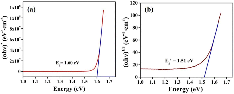
As the results obtained from absorption spectrum, the dependence of the direct and indirect transitions of photons with the absorption coefficient (α) is represented as,42| | | αhν = A(hν − Eg)r (direct) | (6) |
| |  | (7) |
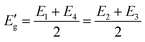
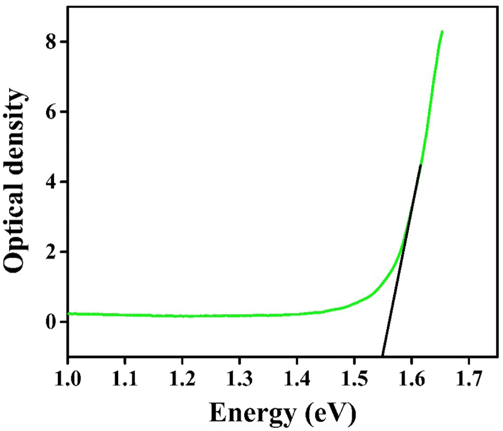
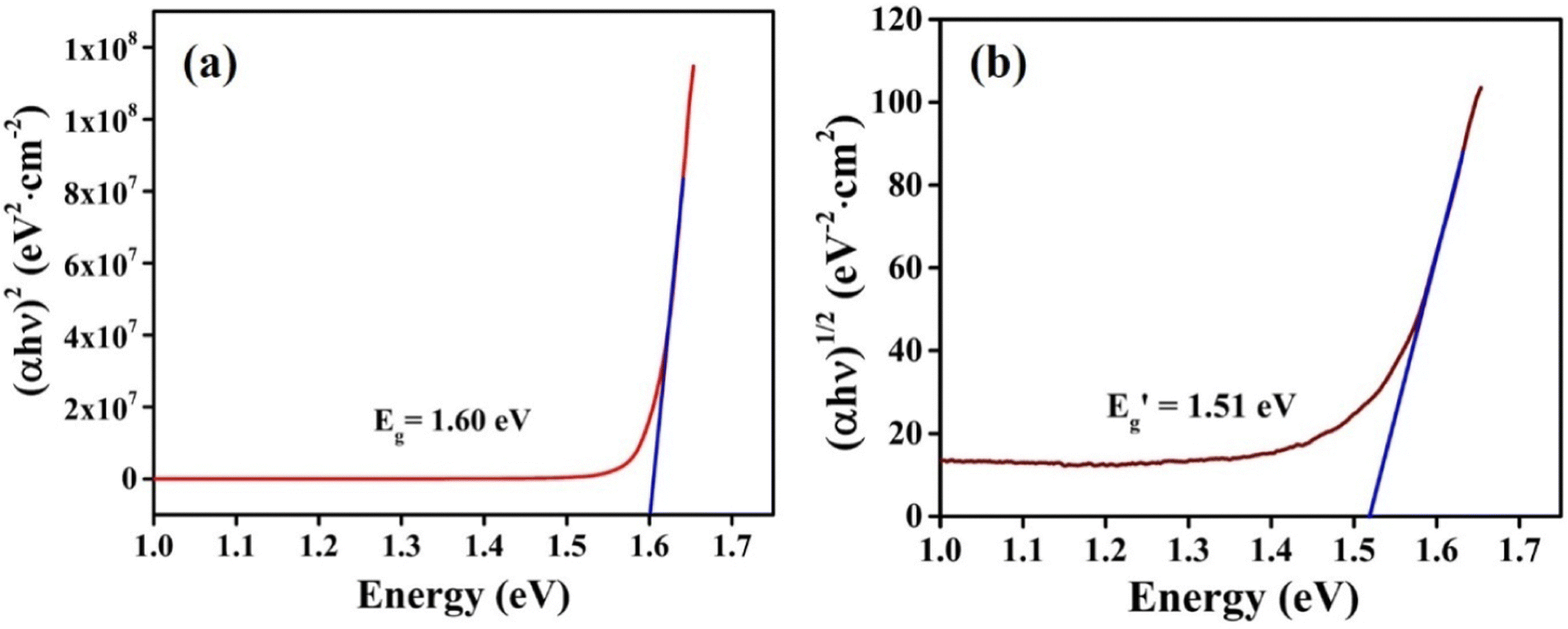
where Eg stands for the energy for the direct transition,  for indirect transition, Epj for phonon energy helping at the indirect transition, and hν for photon energy. The parameters A and B rely more intricately on photon energy, phonon energy Ep, and temperature. Eqn (6) and (7), which are frequently utilised when analysing the results of absorption spectra derived for semiconducting materials, are sufficient to interpret experimental outcomes at a constant temperature. Different values of the constants A and B indicate which transitions are permitted and which are prohibited, and the exponent r in the aforementioned equations varies from 1/2 for direct transitions to 2 for indirect transitions depending on whether or not they are symmetric. It is feasible to ascertain the direct and indirect bandgap for the CIS single crystal by plots of (αhν)2 and (αhν)1/2versus incident photon energy, as depicted in Fig. 12(a and b). The direct and indirect bandgaps obtained from Fig. 12 are 1.60 eV and 1.51 eV, respectively.
 |
| | Fig. 12 The (a) direct, and (b) indirect optical bandgap of the CIS single crystal. | |
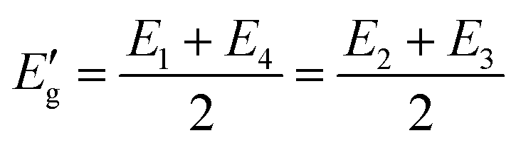
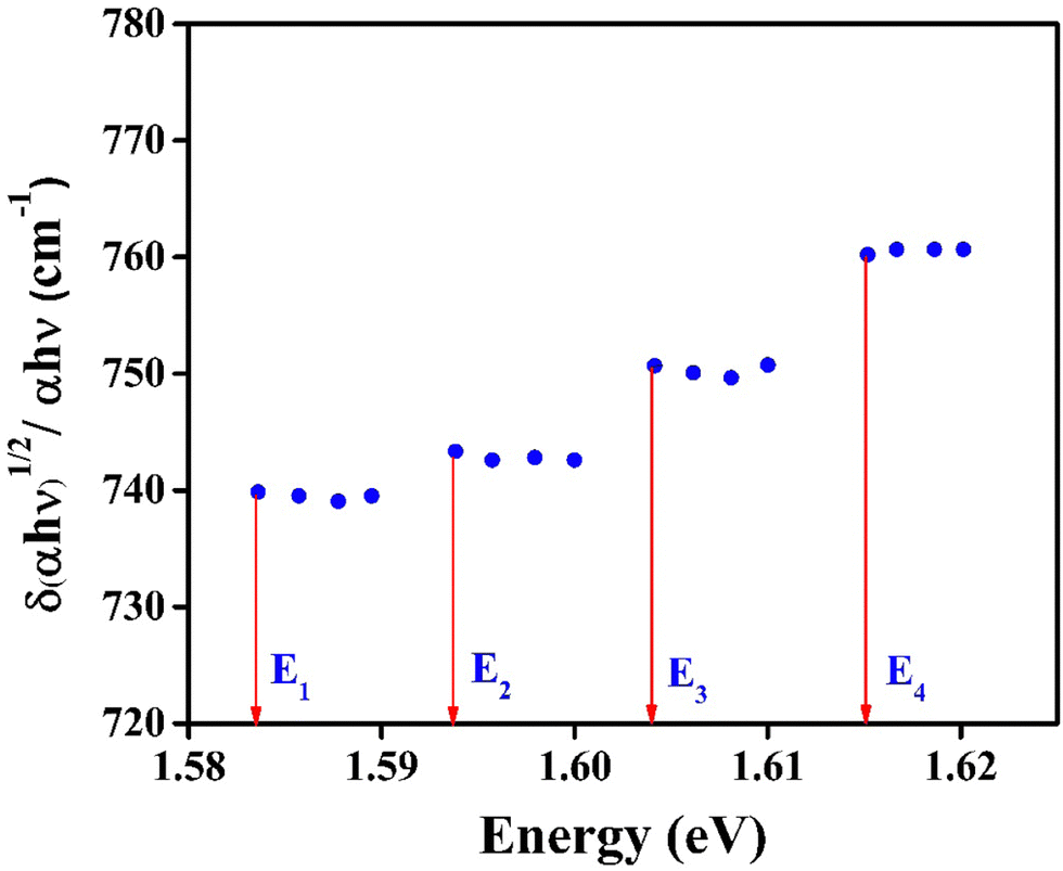
The curves point to a discontinuous straight line, as seen in Fig. 13. They could very well represent an indirect demonstration of how the derivation δ(αhν)1/2/δhν depends on hν involving interband transition of phonon emission or absorption. It is evident from the figure that the derivation is an energy step function consisting of four steps in the well-defined range of E1< E < E2, E2< E < E3, E3< E < E4 and E4 < E, and it is expressed as,43
| |  | (8) |
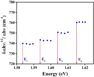 |
| | Fig. 13 The step energies of indirect phonon transition in the CIS single crystal. | |
The energy of the phonons is determined by,44
| |  | (9) |
From the phonon energies, phonon equivalent temperatures are calculated as,
| |  | (10) |
where
kB is the Boltzmann constant.
The step energies, phonon energies and their equivalent temperatures are listed in Table 1.
Table 1 Optical parameters of CIS single crystals
|
E
cut-off (eV) |
1.68 |
|
E
1 (eV) |
1.58 |
|
E
2 (eV) |
1.59 |
|
E
3 (eV) |
1.60 |
|
E
4 (eV) |
1.61 |
 (eV) (indirect) (eV) (indirect) |
1.51 |
|
E
g (eV) (direct) |
1.60 |
|
E
p1 (eV) |
0.015 |
|
E
p2 (eV) |
0.005 |
|
θ
1 (K) |
674 |
|
θ
2 (K) |
224 |
| Band tailing, EU (eV) |
0.056 |
Actual band gap  (eV) (eV) |
1.454 |
| Steepness parameter (s) |
2.19 |
| Electron–phonon interaction (Ee−p) |
0.305 |
4.4. Dielectric constants
Dielectric constant (ε = ε1 + iε2), which is a function of its real and imaginary components, is related to the optical refractive index (η) and extinction coefficient (k) as,45
From eqn (11) and (12), we get,
| | | 4η4 − 4η2ε1 – ε22 = 0 | (13) |
Different values of η can be acquired by solving eqn (13). The positive and real value of 'η’ is utilised to obtain the extinction coefficient from eqn (14). The wavelength-dependent reflectance (R), transmittance (T), and absorption coefficient (α) under normal incidence are given by,46
| | | R = [(η − 1)2 + k2]/[(η2 + 1) + k2] | (15) |
The absorption coefficient (α) in eqn (16) is determined using the equation,
where
λ denotes the wavelength associated with incident photons.
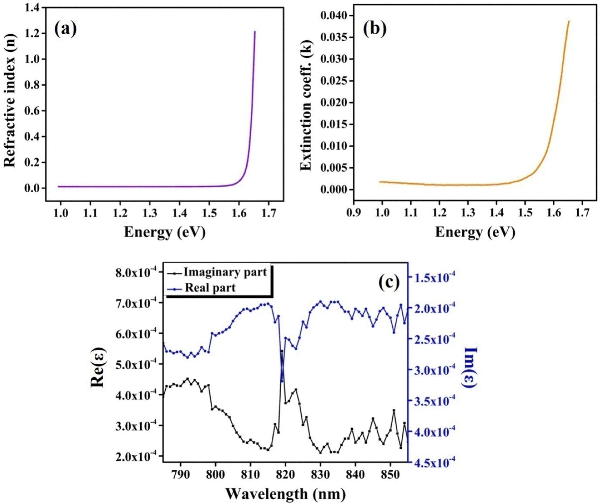
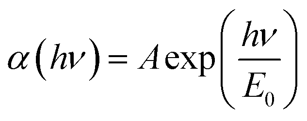
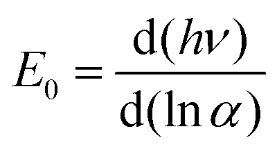
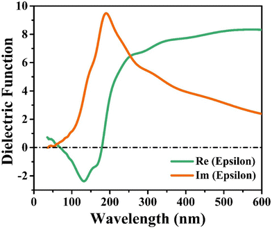
Fig. 14(a and b) represents the refractive index (η) and extinction coefficient (k) variation of CIS single crystals with photon energy. Maximum values for the refractive index (η) and extinction coefficient (k) are found to be 1.22 and 0.039, respectively. Fig. 14(c) clearly illustrates the variation of the real and imaginary dielectric constants with incident photon wavelength. The wavelength corresponding to the intersection of the real and imaginary dielectric functions is 819 nm, which is closer to the absorption band edge (797 nm).
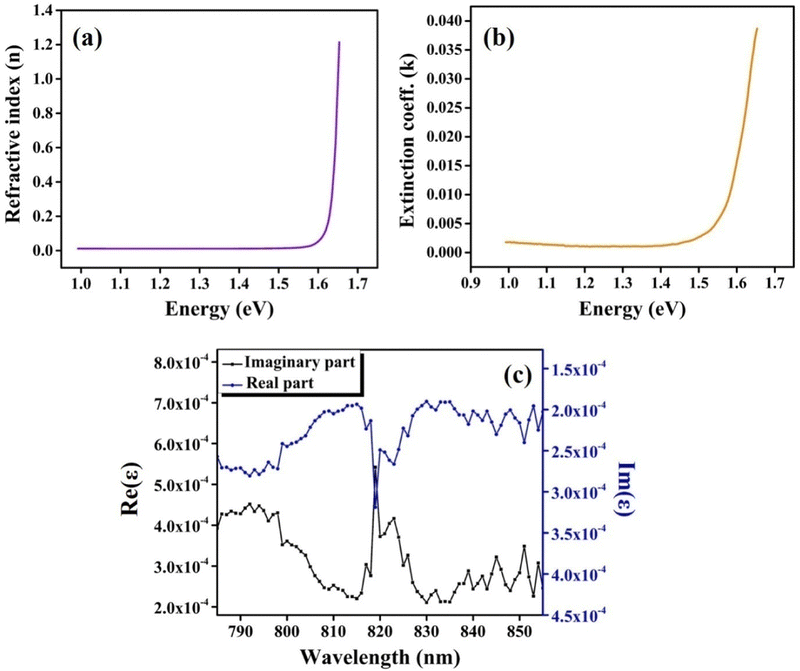 |
| | Fig. 14 (a) Refractive index; (b) extinction coefficient variations with photon energy, and (c) variation of real and imaginary dielectric constants with photon wavelength. | |
4.5. Urbach energy
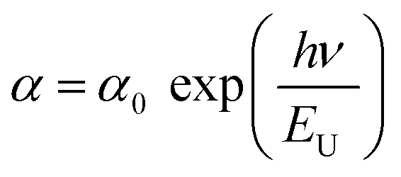
The impurity bands are an evident result of higher impurity concentration; there is also another significant effect that results from the creation of tails that extend the bands to the energy gap, which has drawn a lot of theoretical attention. The valence holes are attracted to an ionised donor, whereas the conduction electrons are attracted to it. Impurities are dispersed at random throughout the host crystal, and thus the strength of the local interaction varies depending on where the impurities are crowded. According to investigations in the low-energy area of the absorption spectrum, the band gap is caused by the occurrence of potential fluctuations in the crystal, which are seen both at the top and bottom of the valence band and typically exhibit an exponential pattern. The formula of the absorption coefficient is:| |  | (18) |
where hν and A represent photon energy and a constant depending on concentration, respectively. The value of E0 is calculated from the absorption edge slope,| |  | (19) |
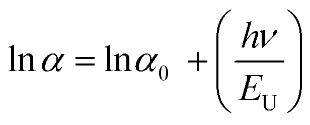
The optical absorption spectrum of the CIS single crystal plays a crucial function as it reveals important details about the composition and optical bandgap. The Urbach empirical rule is implemented to describe the relationship between absorption coefficient (α) and photon energy (hν) in the low photon energy region as,
| |  | (20) |
From eqn (20),
| |  | (21) |
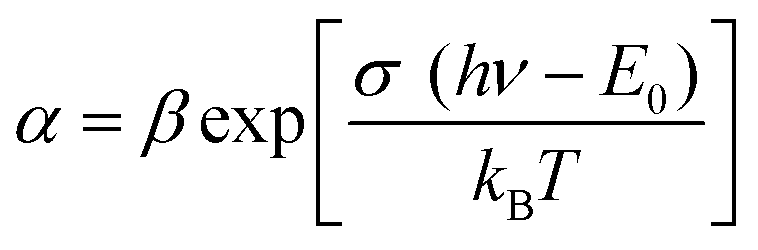
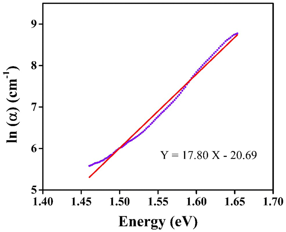
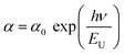
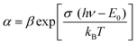
The absorption band tail or Urbach energy (EU) is estimated by potting ln(α) vs. hν (Fig. 15). The slope of the best-fitted line provides EU as 0.056 eV. Urbach suggested another formula in which the absorption coefficient (α) depends on the transition energy (E0), pre-exponential constant (β), incident photon energy (hν), and transition temperature (∼298 K) as,47
| |  | (22) |
 |
| | Fig. 15 The ln(α) versus photon energy curve. | |
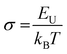
The steepness parameter (σ) is estimated by considering E0 = Eg for direct transition. Using eqn (22)σ can be evaluated from the equation as,
| |  | (23) |
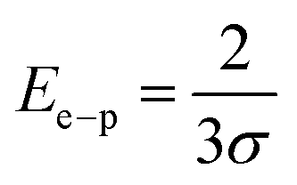
The value of σ is found as 2.19. Electron–phonon interaction strength (Ee−p) is estimated using the equation as,48
| |  | (24) |
The value of Ee−p is found to be 0.305 and all the estimated optical parameters are listed in Table 1.
5. Conclusion
CIS single crystals are synthesised using the CVT technique using iodine as a transporting agent. First principles study is accomplished to predict the band structure and DOS, including optical features like conductivity, reflectivity, refractive index, loss function, dielectric function, and absorption coefficient. The GGA–PBE approach is utilised for the density functional computation method. The DOS revealed that the valence bands at 0.8 eV are mostly a result of hybridisation between In(5p) and S(3p) levels, with a slight input from Cu(3d). Photoconductivity of the crystal begins with photon energy corresponding to 130 nm. High reflectivity occurs in the low-energy area. The peak heights corresponding to refractive index and extinction coefficient are 240 nm and 190 nm, respectively. Two absorption peaks are observed at 50 nm and 140 nm wavelengths, attributed to an inter-band transition between Cu(3d) state in conduction band and In(3p) level in valence band. Loss function peak is observed at 75 nm and corresponds to trailing edges of reflection spectrum. The absorption peak at 195 nm wavelength is related to the electronic transition between the valence band of the Cu(3d) state and conduction band of the In(3d) state. Furthermore, the optical band edge is observed at 797 nm wavelength. The values of Ecut-off and λcut-off are found as 1.68 eV and 738 nm, respectively. Also, the optical direct and indirect bandgap values are estimated to be 1.60 eV and 1.51 eV, respectively. The highest refractive index and extinction coefficient values are estimated to be 1.22 and 0.039, respectively. The wavelength corresponding to intersection of the real and imaginary dielectric functions is 819 nm which is closer to the absorption band edge (797 nm). The band tailing or Urbach energy is calculated as 0.056 eV that allows predicting an accurate indirect bandgap as 1.454 eV. The steepness parameter and electron–phonon interaction strength seemed to be 2.19 and 0.305, respectively.
The electronic and optical parameter findings suggest the CIS single crystal to be a promising material for a wide range of applications ranging to photovoltaics, photodetectors, light-emitting diodes, thermoelectric devices, and so on. The CIS can be used in photoelectrochemical cells to convert light energy into chemical energy. In electrochromic devices, they change their optical properties in response to an applied electric field to find use in smart windows, displays and privacy glass to regulate transparency and light transmission. The material can also find applications in photonic integrated circuits, laser diodes, and other similar devices. As investigation into this versatile material progresses, new applications may be discovered and developed.
Author contributions
RKG contributed to the material preparation, data collection, analysis, and writing of the original draft. SHC assisted in project administration, reviewing, and editing of the manuscript. MSD participated in the data analysis, and methodology. SRB participated in the conceptualisation, investigation, and analysis. AJK participated in reviewing, and editing of the manuscript. RMK participated in data analysis, and methodology. MPD participated in project administration, and acquired resources. MBS participated in the investigation, and data analysis.
Conflicts of interest
There are no conflicts to declare.
References
- W.-Y. Lee, M.-S. Kang, G.-S. Kim, J. W. Choi, N.-W. Park, Y. Sim, Y.-H. Kim, M.-J. Seong, Y.-G. Yoon, E. Saitoh and S.-K. Lee, ACS Nano, 2022, 16, 3404–3416 CrossRef CAS PubMed.
- M.-S. Kang, W.-Y. Lee, Y.-G. Yoon, J. W. Choi, G.-S. Kim, S.-H. Kim, N.-W. Park and S.-K. Lee, ACS Appl. Mater. Interfaces, 2022, 14, 51881–51888 CrossRef CAS PubMed.
- A. J. Khimani, S. H. Chaki, R. K. Giri, R. R. Meena, R. M. Kannaujiya and M. P. Deshpande, Chem. Thermodyn. Therm. Anal., 2023, 100104 CrossRef.
- R. K. Giri, S. H. Chaki, A. J. Khimani, S. R. Patel and M. P. Deshpande, Eur. Phys. J. Plus, 2021, 136, 320 CrossRef CAS.
- R. M. Kannaujiya, S. H. Chaki, A. J. Khimani, A. B. Hirpara, Z. R. Parekh, R. K. Giri, S. Patel and M. P. Deshpande, J. Mater. Sci.: Mater. Electron., 2022, 33, 20823–20836 CrossRef CAS.
- Z. S. Kachhia, S. H. Chaki, R. K. Giri, Z. R. Parekh, R. M. Kannaujiya, A. B. Hirpara, M. P. Deshpande and J. P. Tailor, Mater. Today Proc., 2023 DOI:10.1016/j.matpr.2023.02.240.
- C. Lane and J.-X. Zhu, Phys. Rev. Mater., 2022, 6, 94001 CrossRef CAS.
- F. Xiao, W. Lei, W. Wang, C. Autieri, X. Zheng, X. Ming and J. Luo, Phys. Rev. B, 2022, 105, 115110 CrossRef CAS.
- T. J. Malek, S. H. Chaki, R. K. Giri and M. P. Deshpande, Appl. Phys. A: Mater. Sci. Process., 2022, 128, 830 CrossRef CAS.
- S. Bharucha, M. Dave and R. Vaidya, Mater. Today Proc., 2022, 55, 118–121 CrossRef CAS.
- S. Roy and P. Bermel, IEEE J. Photovoltaics, 2022, 12, 1184–1191 Search PubMed.
- H. Pervaiz, Z. S. Khan, N. Shahzad, N. Ahmed and Q. Jamil, Mater. Chem. Phys., 2022, 290, 126602 CrossRef CAS.
- R. K. Giri, S. Chaki, A. J. Khimani, Y. H. Vaidya, P. Thakor, A. B. Thakkar, S. J. Pandya and M. P. Deshpande, ACS Omega, 2021, 6, 26533–26544 CrossRef CAS PubMed.
- A. B. Hirpara, S. H. Chaki, R. M. Kannaujiya, A. J. Khimani, Z. R. Parekh, Y. H. Vaidya, R. K. Giri and M. P. Deshpande, Appl. Surf. Sci. Adv., 2022, 12, 100338 CrossRef.
- R. M. Kannaujiya, S. H. Chaki, A. J. Khimani, R. K. Giri, A. B. Hirpara, Y. H. Vaidya and M. P. Deshpande, Chem. Phys. Impact, 2023, 100219 CrossRef.
- S. R. Patel, S. H. Chaki, R. K. Giri, A. J. Khimani, Y. H. Vaidya, P. Thakor, A. B. Thakkar and M. P. Deshpande, ACS Appl. Bio Mater., 2023, 6, 2211–2225 CrossRef CAS PubMed.
- H. Liu, X. Yang, K. Wang, Y. Wang, M. Wu, X. Zuo, W. Yang and B. Zou, ACS Appl. Nano Mater., 2020, 3, 2438–2446 CrossRef CAS.
- D. Reishofer, T. Rath, H. M. Ehmann, C. Gspan, S. Dunst, H. Amenitsch, H. Plank, B. Alonso, E. Belamie, G. Trimmel and S. Spirk, ACS Sustainable Chem. Eng., 2017, 5, 3115–3122 CrossRef CAS.
- C. Tablero, Chem. Phys. Lett., 2010, 499, 75–78 CrossRef CAS.
- A. D. P. Leach and J. E. Macdonald, J. Phys. Chem. Lett., 2016, 7, 572–583 CrossRef CAS PubMed.
- R. Klenk, J. Klaer, R. Scheer, M. Lux-Steiner, I. Luck, N. Meyer and U. Ruhle, Thin Solid Films, 2005, 480, 509–514 CrossRef.
- S. Levcenko, N. N. Syrbu, V. E. Tezlevan, E. Arushanov, S. Doka-Yamigno, T. Schedel-Niedrig and M. C. Lux-Steiner, J. Phys.: Condens. Matter, 2007, 19, 456222 CrossRef.
- J. González and C. Rincón, J. Appl. Phys., 1989, 65, 2031–2034 CrossRef.
- N. Nishikawa, I. Aksenov, T. Shinzato, T. Sakamoto and K. S. Katsuaki Sato, Jpn. J. Appl. Phys., 1995, 34, L975 CrossRef CAS.
- R. T. Barradas, C. Rincón, J. González and G. S. Pérez, J. Phys. Chem. Solids, 1984, 45, 1185–1187 CrossRef.
- J. P. Perdew, K. Burke and M. Ernzerhof, Phys. Rev. Lett., 1996, 77, 3865–3868 CrossRef CAS PubMed.
- P. Giannozzi, S. Baroni, N. Bonini, M. Calandra, R. Car, C. Cavazzoni, D. Ceresoli, G. L. Chiarotti, M. Cococcioni, I. Dabo, A. Dal Corso, S. de Gironcoli, S. Fabris, G. Fratesi, R. Gebauer, U. Gerstmann, C. Gougoussis, A. Kokalj, M. Lazzeri, L. Martin-Samos, N. Marzari, F. Mauri, R. Mazzarello, S. Paolini, A. Pasquarello, L. Paulatto, C. Sbraccia, S. Scandolo, G. Sclauzero, A. P. Seitsonen, A. Smogunov, P. Umari and R. M. Wentzcovitch, J. Phys.: Condens. Matter, 2009, 21, 395502 CrossRef PubMed.
- P. Hervé and L. K. J. Vandamme, Infrared Phys. Technol., 1994, 35, 609–615 CrossRef.
- M. Sahnoun, C. Daul, R. Khenata and H. Baltache, Eur. Phys. J. B, 2005, 45, 455–458 CrossRef CAS.
- J. Zheng, C.-H. Lin and C. H. Kuo, J. Appl. Phys., 1997, 82, 792–797 CrossRef CAS.
- A. Chaiken, K. Nauka, G. A. Gibson, H. Lee, C. C. Yang, J. Wu, J. W. Ager, K. M. Yu and W. Walukiewicz, J. Appl. Phys., 2003, 94, 2390–2397 CrossRef CAS.
- S. J. Lim, A. Schleife and A. M. Smith, Nat. Commun., 2017, 8, 14849 CrossRef CAS PubMed.
- N. Feldberg, J. D. Aldous, P. A. Stampe, R. J. Kennedy, T. D. Veal and S. M. Durbin, J. Electron. Mater., 2014, 43, 884–888 CrossRef CAS.
- M. B. Solanki, J. H. Joshi, P. M. Vyas, M. J. Joshi and B. B. Parekh, Invertis J. Sci. Technol., 2017, 10, 98–103 CrossRef.
- M. B. Solanki, P. Patel, S. Shinde, B. B. Parekh and M. Joshi, Ferroelectrics, 2021, 571, 1–25 CrossRef CAS.
- W. Tang, S. Rassay and N. Ravindra, Madridge J. Nanotechnol., 2017, 2, 59–65 Search PubMed.
- R. K. Giri, S. H. Chaki, A. J. Khimani and M. P. Deshpande, J. Alloys Compd., 2023, 959, 170487 CrossRef CAS.
- M. El-Hagary, M. Emam-Ismail, E. R. Shaaban and A. El-Taher, Radiat. Phys. Chem., 2012, 81, 1572–1577 CrossRef CAS.
- A. S. Hassanien and A. A. Akl, J. Alloys Compd., 2015, 648, 280–290 CrossRef CAS.
- A. S. Hassanien and A. A. Akl, Superlattices Microstruct., 2016, 89, 153–169 CrossRef CAS.
- Z. N. Kayani, M. Anjum, S. Riaz, S. Naseem and T. Zeeshan, Appl. Phys. A: Mater. Sci. Process., 2020, 126, 197 CrossRef CAS.
- M. Dave, K. R. Patel and R. Vaidya, Int. J. Phys., Chem. Math. Sci., 2013, 3, 119–126 Search PubMed.
- M. P. Deshpande, G. K. Solanki and M. K. Agarwal, Mater. Lett., 2000, 43, 66–72 CrossRef CAS.
- M. Dave, Bull. Mater. Sci., 2015, 38, 1791–1796 CrossRef CAS.
- E. Turan, M. Kul, A. S. Aybek and M. Zor, J. Phys. D: Appl. Phys., 2009, 42, 245408 CrossRef.
- S. S. P. Parkin and A. R. Beal, Philos. Mag. B, 1980, 42, 627–642 CAS.
- J. Singh, V. Verma, R. Kumar and R. Kumar, Results Phys., 2019, 13, 102106 CrossRef.
- V. Dalouji, N. Rahimi and S. Goudarzi, Mech. Adv. Mater. Struct., 2022, 29, 6634–6647 CrossRef CAS.
|
| This journal is © The Royal Society of Chemistry 2023 |
Click here to see how this site uses Cookies. View our privacy policy here. 
 Open Access Article
 This Open Access Article is licensed under a Creative Commons Attribution-Non Commercial 3.0 Unported Licence
 *a,
Sunil H.
Chaki
*ab,
Mehul S.
Dave
c,
Shivani R.
Bharucha
c,
Ankurkumar J.
Khimani
d,
Rohitkumar M.
Kannaujiya
a,
Milind P.
Deshpande
a and
Mitesh B.
Solanki
e
*a,
Sunil H.
Chaki
*ab,
Mehul S.
Dave
c,
Shivani R.
Bharucha
c,
Ankurkumar J.
Khimani
d,
Rohitkumar M.
Kannaujiya
a,
Milind P.
Deshpande
a and
Mitesh B.
Solanki
e


 for indirect transition, Epj for phonon energy helping at the indirect transition, and hν for photon energy. The parameters A and B rely more intricately on photon energy, phonon energy Ep, and temperature. Eqn (6) and (7), which are frequently utilised when analysing the results of absorption spectra derived for semiconducting materials, are sufficient to interpret experimental outcomes at a constant temperature. Different values of the constants A and B indicate which transitions are permitted and which are prohibited, and the exponent r in the aforementioned equations varies from 1/2 for direct transitions to 2 for indirect transitions depending on whether or not they are symmetric. It is feasible to ascertain the direct and indirect bandgap for the CIS single crystal by plots of (αhν)2 and (αhν)1/2versus incident photon energy, as depicted in Fig. 12(a and b). The direct and indirect bandgaps obtained from Fig. 12 are 1.60 eV and 1.51 eV, respectively.


 (eV) (indirect)
 (eV)
(eV)