
 Open Access Article
 This Open Access Article is licensed under a Creative Commons Attribution-Non Commercial 3.0 Unported Licence
Investigation of the reliability of nano-nickel/niobium oxide-based multilayer thin films deposited on polymer substrates for flexible electronic applications†
Rahul
Sahay
 *ag,
Yen-Cheng
Tu
b,
Izzat
Aziz
c,
Arief S.
Budiman
*adef,
Cher Ming
Tan
bi,
Pooi See
Lee
c,
Olivier
Thomas
g and
Nagarajan
Raghavan
*h
*ag,
Yen-Cheng
Tu
b,
Izzat
Aziz
c,
Arief S.
Budiman
*adef,
Cher Ming
Tan
bi,
Pooi See
Lee
c,
Olivier
Thomas
g and
Nagarajan
Raghavan
*h
aXtreme Materials Lab, Engineering Product Development (EPD) Pillar, Singapore University of Technology and Design (SUTD), 487372, Singapore. E-mail: rahul@sutd.edu.sg; suriadi@alumni.stanford.edu
bCenter for Reliability Sciences and Technologies (CReST), Department of Electronic Engineering, Chang Gung University, Taiwan
cSchool of Materials Science and Engineering, Nanyang Technological University, 639798, Singapore
dDepartment of Manufacturing and Mechanical Engineering and Technology, Oregon Institute of Technology, Klamath Falls, OR 97601, USA
eIndustrial Engineering Department, BINUS Graduate Program-Master of Industrial Engineering, Bina Nusantara University, Jakarta 11480, Indonesia
fOregon Renewable Energy Center (OREC), Klamath Falls, OR 97601, USA
gAix-Marseille Univ., CNRS, Univ. de Toulon, IM2NP UMR 7334, 13397 Marseille, France
hNano-Micro Reliability Lab (MRL), Engineering Product Development (EPD) Pillar, Singapore University of Technology and Design (SUTD), 487372, Singapore. E-mail: nagarajan@sutd.edu.sg
iDepartment of Radiation Oncology, Chang Gung Memorial Hospital, Taoyuan 333, Taiwan
First published on 23rd June 2023
Abstract
Flexible electronics are attractive for a range of applications, such as wearable gadgets and personalized medicine, because of their flexibility, stretchability, and adaptability. However, the reliability of such devices, both mechanical and electrical, is a bottleneck for their widespread application across different use-case scenarios. Here, we report the reliability of nickel–niobium oxide (crystalline–amorphous) sandwich nanolayers on a PI substrate (Ni–Nb2O5–PI) compared to pure nickel (Ni) nanolayers on a PI substrate (Ni–PI) as a potential candidate for electrodes or interconnects for flexible electronic or energy devices. A tailored rate-dependent bending failure/fracture test system was used to analyze the electrical resistance (oscillations) as a function of the loading cycles of the sample deposited on polyimide (PI) (the compliant substrate). Resistance oscillation amplitude during the rate-dependent bending failure/fracture test for Ni–PI (∼6%) was higher compared to that of Ni–Nb2O5–PI (∼2%), suggesting a low resistance change and consequently low mechanical deformation for Ni–Nb2O5–PI. Nanoindentation experiments were also performed to ascertain the hardness and reduced elastic modulus of the samples. Hardness of Ni–PI (∼1.4 GPa) was lower compared to that of Ni-Nb2O5-PI (∼2.4 GPa) suggesting high flow strength for Ni–Nb2O5–PI. Therefore, the incorporation of amorphous niobium oxide into samples otherwise composed of Ni nanolayers significantly improved their fatigue/fracture strength with a slight reduction in electrical conductivity with appreciably low resistance oscillation (amplitude) essential for operational reliability of flexible devices. We also demonstrated that the nickel–niobium oxide/polyimide stack was electrically/mechanically stable up to 500 K stress cycles at a bending radius of 8.5 mm.
Introduction
Flexible electronics have been explored for human–machine interface applications ranging from flexible displays to compliant wearable devices, personalized medicine, and health monitoring sensors.1–3 Flexibility of electronic devices is achieved through the use of compliant substrates and by the introduction of flexible conductors or electrodes. Three approaches are generally used to achieve flexible electronics using compliant substrates: (1) thin metal films, (2) silicon/thin glass, and (3) polymer substrates or paper cellulose substrates.4 Although thin metal substrates offer considerable mechanical strength, corrosion resistance, and high temperature tolerance,5 they suffer from limited bendability and overall achievable thickness.6 Silicon/glass substrates offer high temperature resistance.7 Thin glass substrates also offer high light transmittance. However, thin silicon/glass substrates have poor bendability and machinability. Therefore, there has been an increased emphasis on polymers as substrates to achieve flexibility in electronic devices due to their compliance and pliability.8 The polymers commonly used as substrates are polycarbonate (PC),9 polyvinyl fluoride (PVDF),10 poly(etheretherketone) (PEEK),11 polyethylene terephthalate (PET),12 poly(dimethylsiloxane) (PDMS),13 and chemically and thermally stable polyimide (PI)14,15 as well as natural polymers.16 Although the maximum operating temperature of polymer substrates is lower than that of metal, silicon or glass substrates, they could still provide the compliance and versatility required for flexible electronics.12Approaches to achieving electrode flexibility in electronic devices include the use of corrugated/serpentine metal structures on polymer substrates.17 Although these devices offer some degree of flexibility, they are still not scalable because appropriate manufacturing processes must be developed for their mass production. Other approaches include the fabrication of metal-alloys,18 liquid metals,19 ionic conductors,20 crystalline–amorphous nanolaminates,21–23 metal–metal laminates24,25 and metal-ceramic laminates,26–28 Typically, it should be noted that nanolaminates/nanolayers with an inherently high interfacial area/volume ratio and a controllable layer thickness exhibit improved resistance to crack initiation/propagation and thus achieve high fatigue/fracture resistance compared to that of their bulk metallic counterparts.29 Specifically, the fatigue/fracture resistance of the metal–metal nanolaminate/nanolayers is enhanced with the reduction of the layer thickness; nevertheless, they lack ductility, which is one of the prerequisites for achieving flexible electronics. One possible method to improve ductility of the nanolaminates/nanolayers is the introduction of an amorphous phase into the otherwise crystalline structure. Amorphous metals deform through the shear transformation zones (STZs) (which propagate and join to form a shear band), whereas crystalline materials deform through the propagation/pile-up of dislocations; nevertheless, synergistic interactions between crystalline and amorphous phases (mainly at the interface) have the capability of achieving strong and ductile nanolaminates/nanolayers21–23 Molecular dynamics (MD) simulation studies have been previously performed to elaborate on the role of amorphous layers in crystalline–amorphous nanolaminates/nanolayers. The results indicate that both crack nucleation and propagation were hindered due to the presence of amorphous layers, leading to enhanced ductility and fracture toughness.30 Similarly, Cheng et al.31 through MD simulations also observed interfacial sliding at the crystalline–amorphous interface, which was attributed to a shear-transformation-zone (STZ) plasticity accommodated by dislocation nucleation and proliferation at the interface.
The DC magnetron sputtering is used for the fabrication of multi-/single-layer thin films in the present work, discussed in subsequent sections. DC magnetron sputtering is a versatile production methodology used to deposit precise, uniform, and compositionally controlled single- or multilayer thin films of various materials onto a variety of substrates.32–34 It involves the use of a direct current (DC) power supply to generate plasma and sputter materials from single or multiple targets onto a substrate. DC magnetron sputtering allows for precise control over deposition parameters such as sputtering power, inlet gas composition, substrate temperature, deposition rate, target composition, pressure, and target–substrate distance, thereby allowing for the precise control of the morphology as well as the stoichiometry of the deposited materials.35,36 In the case of multilayer thin films, DC magnetron sputtering allows for excellent control over the interfacial properties. The technique is widely utilized in industries such as electronic, photocatalytic, sensor, and solar cell to create functional coatings and nano-/microlayers with specific properties.37
In this work, nickel (Ni)–niobium oxide (Nb2O5) nanolayers deposited on a PI substrate are used as the configuration for the electrodes or interconnects of flexible devices. The authors believe that designed crystalline–amorphous nickel (Ni)–niobium oxide (Nb2O5) nanolayers on PI materials also have the potential to play a role in the green economy by being used in energy-efficient technologies such as solar cells, LED lights, and batteries as conductive stretchable electrodes, making them more suitable for flexible applications. Nickel (Ni) thin films fabricated through DC magnetron sputtering are being widely used in various electronic and magnetic applications due to their excellent electrical conductivity and magnetic properties. Typically, the resistivity of nickel thin films fabricated through DC magnetron sputtering depends on films’ microstructure and impurities which are in turn related to films’ composition, deposition parameters, and post-deposition treatments. Typical reported resistivity values for nickel thin films deposited by DC magnetron sputtering range from ∼10 to ∼100 μΩ cm.38 Typically, I–V characterization of nickel thin films deposited by DC magnetron sputtering exhibits a linear behaviour (ohmic behaviour). However, deviations from the ohmic behaviour could occur at high voltages due to non-linear effects or the presence of Schottky barriers at the film–film or film–substrate interface. Similarly, the resistivity of niobium oxide thin films fabricated through DC magnetron sputtering depends on factors such as the film composition, deposition parameters, and post-deposition treatments.39 Reported electrical resistivity values for Nb2O5 thin films deposited by DC magnetron sputtering range from a few to hundred Ω cm,40,41 depending on the deposition parameters and resultant film properties. The electrical resistivity of niobium oxide thin films fabricated through DC reactive magnetron sputtering decreases with the increase of inlet oxygen (O2) pressure due to the increase in the Nb2O5 stoichiometry.42 The nickel and niobium oxide alternating multilayer system helped us to achieve alternating crystalline and amorphous structures on the PI substrate, which are studied in detail in the following sections.
PI was selected as the flexible substrate due to its exceptional ductility and flexibility, while the electrode consists of 10 alternating layers of ∼20 nm nickel (Ni) and ∼20 nm niobium oxide (Nb2O5). The control reference sample used is a 400 nm Ni nanolayer. Although copper (conductivity = 5.9 × 10⁷ S m−1) is widely used in nanolaminates/nanolayers due to its excellent conductivity, other materials such as nickel (1.4 × 10⁷ S m−1), niobium and aluminum are also used along with copper as components of sandwiched nanolayers.43,44 Here, a novel Ni–Nb2O5 nanolayer structure is designed and fabricated to test its reliability as an electrode on a flexible substrate for a flexible device. It is hypothesized that the crystalline layers in the Ni–Nb2O5 nanolayers can provide high strength and stiffness, while the amorphous layers can enhance the film's toughness and ductility. Additionally, the interface between the crystalline and amorphous layers acts as an effective barrier to crack propagation. These properties can lead to improved cyclic fatigue properties of Ni–Nb2O5–PI compared to single-phase Ni–PI. A tailored rate-dependent bending failure/fracture test system is used to investigate the electrical performance of the device under repeated cyclic loading. Nanoindentation experiments were also performed to ascertain hardness and reduced elastic modulus of the samples.
Materials and methods
Device fabrication
Nanometric layers of Ni and Nb2O5 were deposited on PI (0.2 mm) using a direct current (DC) sputtering system. The Ni layers are deposited by DC sputtering at a power of 100 W in ambient argon (Ar) at a pressure of 4.7 mTorr at room temperature using a 99.99% pure Ni target. The Nb2O5 layers are also deposited by DC sputtering at a power of 100 W in ambient argon at a pressure of 4.7 mTorr at room temperature. The 99.99% pure Nb target used has undergone surface oxidation before sputtering and therefore has led to the formation of Nb2O5 nanolayers as further verified using transmission electron microscopy (TEM) and simultaneous energy dispersive X-ray (EDX) analysis discussed in the subsequent sections. Initially, the sputtering chamber is evacuated to a base pressure of 2 × 10⁻⁶ torr before introducing 99.99% pure noble argon. DC sputtering steps were repeated to form multiple alternating layers of Ni and Nb2O5 leading to metal–metal oxide sandwich nanolayers. For the Ni–Nb2O5 nanolayers, 10 layers (thickness = ∼20 nm) of Ni and Nb2O5 were deposited alternately on the PI (see Fig. S6 in the ESI†). The final thickness was the same for the Ni–Nb2O5 nanolayers as for the control Ni nanolayer and was ∼400 nm. For both samples, the nanolayer(s) (both Ni and Nb2O5) were sputtered onto a ∼0.2 mm thick PI substrate using the same vacuum cycle.Test methodology
A customized rate-dependent bending failure/fracture test system45 (EVOtest from Laryee Technology Company) was used for the bending failure/fracture tests of the specimens (see Fig. 1 for the configuration of the test). The tests were conducted in accordance with GB/T 228.1-2010 to measure the change in resistance of the specimens in bending mode under cyclic loading. The specimen was mounted between two plates with a fixed gap (2r ∼17 mm). The upper plate was stationary, while the lower plate was movable. The lower plate moved cyclically parallel to the upper plate. The motion of the lower plate was sinusoidal, with a frequency of 5 Hz and an amplitude of 14 mm. The length and width of the Ni–Nb2O5 nanolayers and Ni nanolayers deposited on PI were 70 mm and 5 mm, respectively. A 0.2 mm thick PI was used as the standard substrate for all the samples studied. Samples with an overall thickness of the nanolayer(s) of ∼400 nm deposited on a PI substrate were tested (see the ESI,† Fig. S1). The resistance during the rate-dependent bending failure/fracture tests was measured using a DC low Ohmmeter (Donghui TH2512+). At least 5 samples for both Ni–Nb2O5–PI and Ni–PI were tested using the rate-dependent bending failure/fracture test.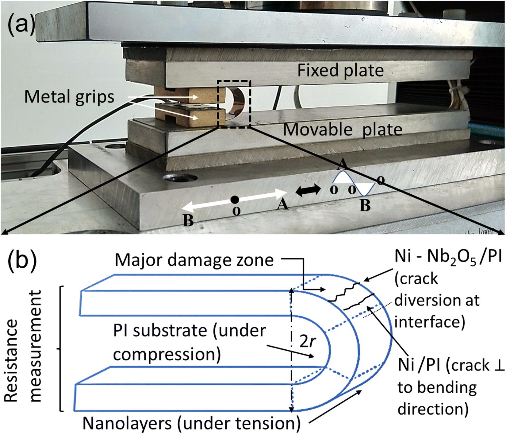 | ||
| Fig. 1 The configuration of the customized rate-dependent bending failure/fracture test, (a) picture of the experimental setup. The upper plate is stationary, while the lower plate is movable. The lower plate moved cyclically parallel to the upper plate. The motion of the lower plate was sinusoidal with a frequency of 5 Hz and an amplitude of 14 mm, (b) schematic of the configuration of the sample shows the substrate (PI) on the inside (compressive state) and the nanolayer(s) on the outside (tensile state). The cracks occur perpendicular to the applied stress, i.e., to the bending direction, in the major damage zone. Representative schematics of cracks are shown for Ni–Nb2O5–PI (crack with diversion at the interface) and nickel/PI (cracks predominately perpendicular to the bending direction), which are discussed in detail in the subsequent paragraphs. | ||
Nanoindentation
Nanoindentation was performed using a TI 950 Tribo-lndenter (Hysitron) with a Berkovich indenter to ascertain the hardness and reduced elastic modulus of the samples. The loading rate was 5 nm s−1, while the unloading rate was 10 nm s−1. The peak displacement ranged from 100 nm to 400 nm and the data were recorded with a displacement resolution of ∼10 nm. Mechanical properties such as hardness and reduced Young's modulus produced by nanoindentation helped in the subsequent analysis of the rate-dependent bending failure/fracture tests.Characterization
The surface morphology and the cross-sectional profiles of the specimens were recorded using a field emission scanning electron microscope (FE-SEM) (JEOL JSM-7600F). SEM is used to observe surface cracks that developed or propagated during the rate-dependent bending failure/fracture tests. TEM (JEOL 2100F with integrated Oxford EDX) at 200 kV in STEM mode was used to study the crack propagation in the samples. Firstly, a focused ion beam (FIB, FEI Nova NanoLab 600i DualBeam) was employed for the preparation of lamellas perpendicular to surface cracks (see ESI,† Fig. S2). Later, both of these lamella samples were mounted on a Cu grid, and were then used to analyse the propagation of cracks along the thickness of the samples by TEM. EDX combined with TEM was also used for determining the composition (in at%) of the components of the layers in the nanolayers.Results
Metal–metal oxide nanolayers
Typically, monolithic metal layers were deposited on polymer substrates to achieve flexibility (while maintaining electrical conductivity) such as bismuth telluride on polyimide.46 Nevertheless, bimetallic nanolayers with higher interfacial density offer better resistance to crack initiation and growth47–50 compared to monolithic metallic layers. However, crystalline/crystalline bimetallic nanolayers lack ductility, which could be improved by the introduction of amorphous layers in the otherwise crystalline/crystalline nanolayers. Here, the transition metals, crystalline Ni (∼10 to ∼100 μΩ cm38) and amorphous Nb2O5 (∼few to hundreds Ω cm40,41), were selected to fabricate crystalline–amorphous nanolayers. It is worth mentioning that the electrical conductivities of Ni and Nb2O5 mentioned are bulk values. In the case of Nb2O5 nanolayers, it should be noted that the decrease in the oxygen flow rate during the fabrication of their thin oxide film through reactive magnetron sputtering induces oxygen vacancies, which therefore increases the conductivity of the film.51 In the present study, it is believed that Nb2O5 was realized due to surface oxidation of the Nb target before sputtering, which was performed in an inert environment. In this scenario, where the oxygen supply is limited, there are high chances for the presence of oxygen vacancies, therefore, resulting in a much higher conductivity of the Nb2O5 nanolayers compared to its bulk value. In other words, our Nb2O5 layers are highly oxygen-deficient, which helps in maintaining high conductivity for Ni–Nb2O5 nanolayers. Furthermore, in the case of the crystalline–amorphous sandwich nanolayers, the interfaces could absorb dislocations (emanating from the crystalline layer) or block shear band propagation (emanating from the amorphous layer)52,53 thereby hindering the initiation/propagation of cracks under continuous cyclic loading. Therefore, the crystalline–amorphous interfaces in the Ni–Nb2O5 nanolayers provide higher fracture/failure resistance compared to the pure Ni nanolayer.EDX combined with TEM was used to determine the composition of the crystalline and amorphous layers of the nanolayered structure (see the ESI,† Fig. S3–S5). The EDX along the cross-section, along the amorphous as well as along the crystalline layers of the Ni–Nb2O5/PI are shown in Fig. S3–S5, respectively, in the ESI.† Theoretically, the atomic percentages (at%) of niobium and oxygen in Nb2O5 are 28.57 (2/7 × 100) and 71.42% (5/7 × 100), respectively, which are found to be close to those measured through the EDX data (see Fig. S3 and S5), ∼27% for niobium and ∼70% for oxygen. The presence of Nb2O5 that is amorphous is further confirmed by TEM (discussed in detail in the analysis regarding TEM).
Nanoindentation analysis
Since the total thickness of Ni–Nb2O5 nanolayers and Ni nanolayer is ∼400 nm, the upper indentation limit is set at 400 nm. It was experimentally observed that the indenter is less sensitive to displacements of less than 100 nm. Therefore, the indentation depth was configured to range between 100 nm and 400 nm. Subsequently, measurements were performed employing a Berkovich indenter with a tip radius of ∼100 nm using a continuous stiffness measurement method at standard temperature and pressure (STP). We attained load vs. displacement curves and then used them to calculate the reduced Young's modulus (Er) and hardness (H) of the samples. The mechanical properties are measured by indenting the samples at different spatial locations along the length of the sample to verify the repeatability of the results. Samples from different batches are also measured and the resultant behaviour of the samples is shown in Fig. 2. Fig. 2(a and b) show the hardness and reduced Young's modulus curves of the Ni–Nb2O5–PI and Ni–PI samples, respectively. In Fig. 2(a), both the samples exhibited similar trends, i.e., a decrease in hardness with indentation depth. Similar trends of hardness and Young's modulus (Er) with indentation depth were observed for metallic nanolayers deposited on either a stiff or compliant substrate.54–56 The hardness of the Ni–Nb2O5–PI is higher than that of the Ni–PI, which can be attributed to the insertion of Nb2O5 into the multilayer structure. For the Berkovich indenter, hardness (H) is correlated with the flow stress, σf, obtained from tensile testing at a strain of ∼8% as H = kσf, where k is Tabor's constraint factor for metallic materials, k ∼ 2.7.57 Therefore, an increase in H signifies a growth in the flow stress/strength of Ni–Nb2O5–PI compared to Ni–PI. Apart from the increase in flow stress, the crystalline–amorphous nanolayers also achieve higher plasticity due to interfacial shear occurring at the crystalline–amorphous interface.23,31 Reduced Young's modulus (Er) was observed to be slightly higher for Ni–PI in comparison to Ni–Nb2O5–PI due to the insertion of Nb2O5 (a modulus of elasticity of ∼137–161 GPa58,59) into Ni (with a modulus of elasticity of ∼207 Pa) (see Table 1).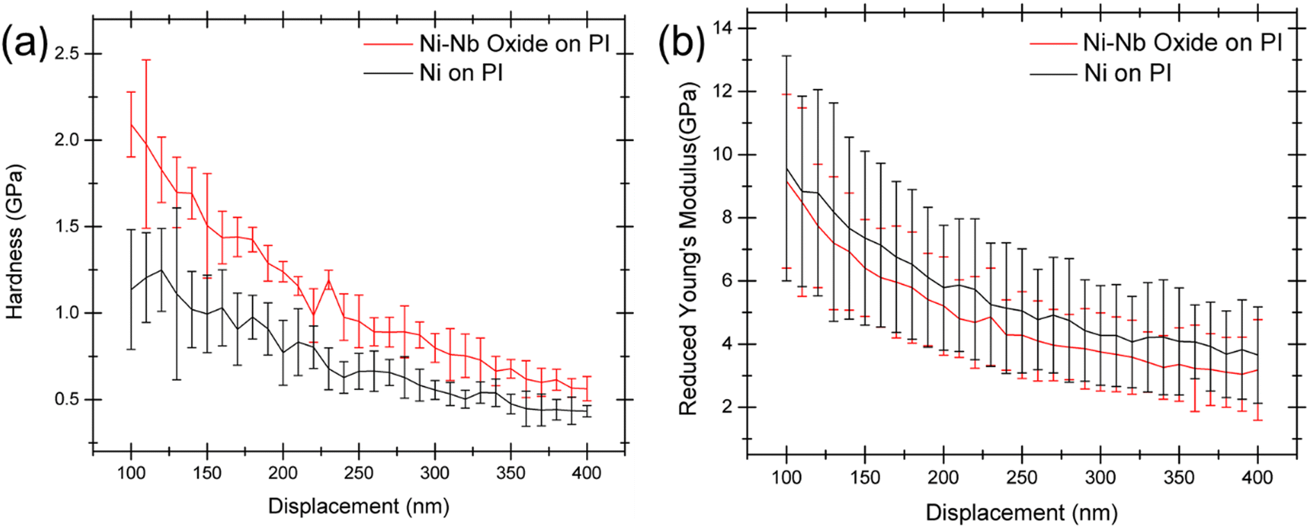 | ||
| Fig. 2 (a and b) show the comparison of hardness and reduced Young's modulus curves (the curves represent the mean values of the parameters, whereas the error bars are SD(Er±) of the Ni–Nb2O5–PI and Ni–PI). | ||
| Samples | Structure | Hardness (GPa) | Resistivity (Ω cm) | ΔR/R% after 0.5 million cycles (%) | Young's modulus (GPa) | Surface crack density per 10 μm2 | Crack dimensions (mean±SD, min., max. μm) per 10 μm2 |
|---|---|---|---|---|---|---|---|
| Ni–Nb2O5–PI | Crystalline-amorphous | ∼2.4 | Nickel (∼10 to ∼100 × 10−6)–niobium oxide (few to hundreds) | ∼115 | Nickel (207)–niobium oxide (∼137–161) | 34 | 1.20 ± 0.69; 0.30, and 3.37 |
| Ni–PI | Crystalline FCC | ∼1.4 | ∼10 to ∼100 × 10−6 | ∼94 | 207 | 111 | 0.76 ± 0.61; 0.22, and 3.88 |
Rate-dependent bending failure/fracture test
The variation in electrical resistance of the Ni–Nb2O5 nanolayers and Ni nanolayers deposited on PI under bending strain was measured using the rate-dependent bending failure/fracture tests. At least 5 samples for both Ni–Nb2O5–PI and Ni–PI were tested. The final resistance for Ni–PI was in the range of ∼0.027–0.033 KΩ whereas the initial resistance was in the range of ∼0.016–0.019 KΩ based on the samples tested for 0.5 million cycles. Similarly, the final resistance for Ni–Nb2O5–PI was in the range of ∼0.110–0.210 kΩ whereas the initial resistance was in the range of ∼0.05–0.09 KΩ based on the samples tested for 0.5 million cycles. The bending strain employed to the samples is inversely proportional to the bending radius (estimated from t/(2r), where t is the overall thickness of the stack and r is the bending radius (see Fig. 1)). The bending strain on the samples was ∼1.16% for t ∼0.2 mm and 2r ∼17 mm. Fig. 3 reveals percentage variations of the resistance normalized by the initial resistance of the samples (ΔR/R%) under a bending strain of ∼1.16%.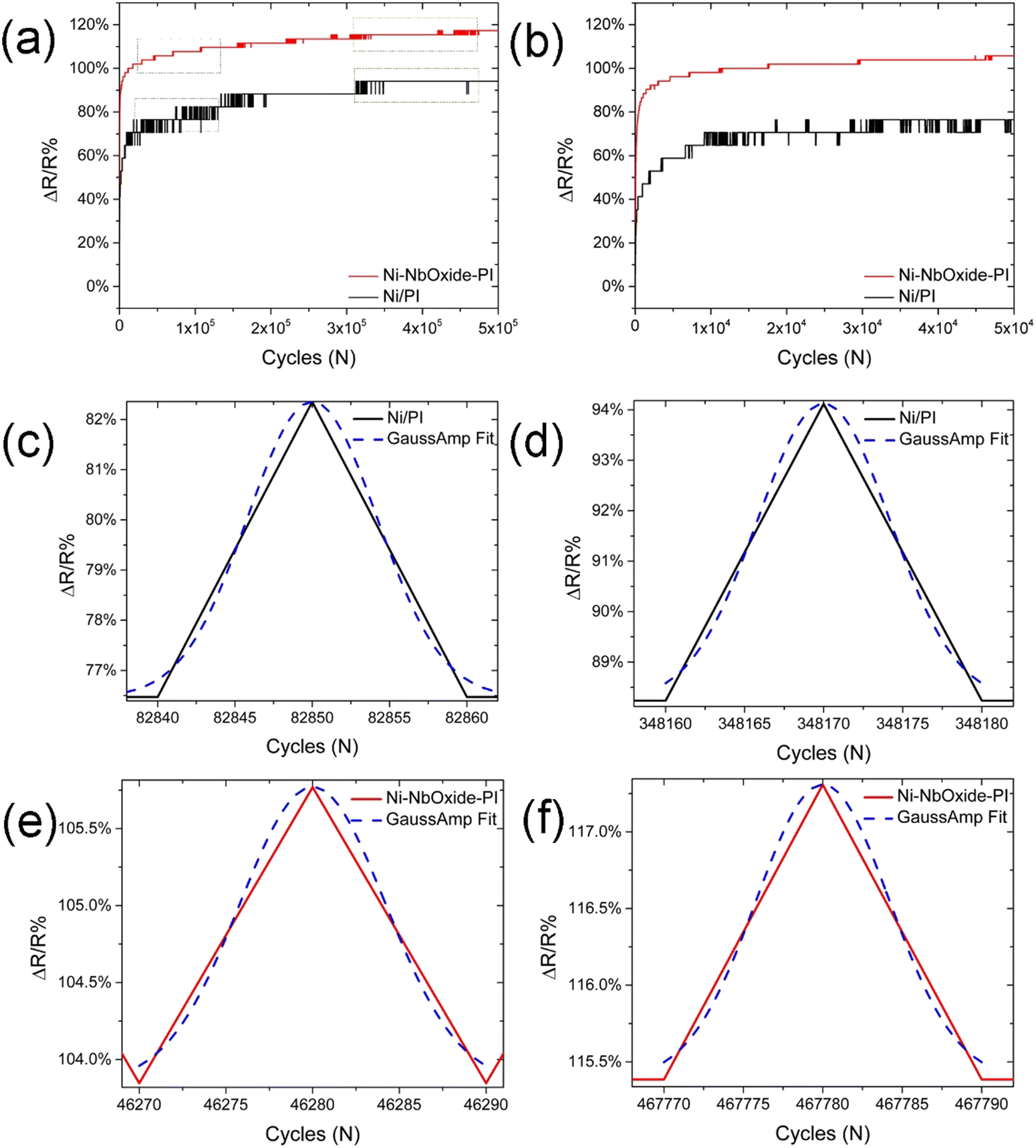 | ||
| Fig. 3 (a and b) ΔR/R% of Ni–Nb2O5–PI and Ni–PI as a function of loading cycles: (a) 5.0 × 10⁴ and (b) 5.0 × 10⁵ cycles. The resistances were normalized by the initial resistances of the samples, (c and d) representative resistance peaks and corresponding Gaussian fits to measure FWHM and amplitude for Ni–PI for initial and final resistance oscillations (shown by the rectangular boxes in (a)), respectively, and (e and f) similarly, representative resistance peaks and corresponding Gaussian fits to measure FWHM and amplitude for Ni–Nb2O5–PI for initial and final resistance oscillations (shown by the rectangular boxes in (a)), respectively. | ||
ΔR/R% increased for both Ni–Nb2O5–PI, and Ni–PI, exhibiting significant growth in the early stages (the first ∼5.0 × 10⁴ cycles) (see Fig. 3(a and b)). The most significant difference between Ni–Nb2O5–PI and Ni–PI was the initial resistance change/oscillation experienced by the Ni–PI sample. It should be noted that up to ∼2.0 × 10⁵ cycles, the Ni–PI sample exhibited considerable resistance oscillations indicating the formation of more microcracks and extrusions for Ni–PI compared to Ni–Nb2O5–PI (see Fig. 3). Fig. 3(c and d) show resistance oscillation peaks and the corresponding Gaussian fits used to measure full width at half maximum (FWHM) values and amplitudes for Ni–PI for initial and final resistance oscillations, respectively, and Fig. 3(e and f) similarly show resistance oscillation peaks and the corresponding Gaussian fits for Ni–Nb2O5–PI for initial and final resistance oscillations, respectively. The amplitude of the resistance oscillations can be used to study the mechanical deformation of the samples. The resistance oscillation peaks in Fig. 3(c–f) show no major variation in the amplitude over cycles for the samples, although the amplitude for Ni–PI was higher than that for Ni–Nb2O5–PI with negligible low resistance (LR) drift. The LR drift typically determines the mechanical stability of a sample against externally applied stress. Although the LR drift is negligible, the high resistance oscillation amplitude for Ni–PI (∼6%) compared to Ni–Nb2O5–PI (∼2%) suggests a high resistance change and consequently higher mechanical deformation. Therefore, negligible LR drift with low resistance oscillation amplitude suggests that the incorporation of Nb2O5 nanolayers into the Ni nanolayers strongly improved their electromechanical robustness.
Furthermore, the FWHM for a resistance peak can be a measure of applied strain and the electronic structure of the sample over time. The decrease in FWHM (sharpening of the resistance peak waveform) is an indication of an increase in the rate of resistance (with respect to cycles) signalling an increase in the applied strain in the sample. The ΔR/R% vs. cycle curves for both samples feature highly non-repeatable resistance oscillation peaks as compared to distinctive and repeatable resistance peaks for pure metals with growing cycle numbers. This can be attributed to two- and three phase systems for Ni–PI and Ni–Nb2O5–PI, respectively, compared to a single-phase system for pure metals (see Fig. 3 and Fig. S7, S8 in the ESI†). FWHM for a representative resistance oscillation peak (see Fig. 3(c–f)) is ∼9.89 cycles for both the samples, which were found to be unchanged from the early resistance oscillation peaks to the final resistance oscillation peaks, which shows that applied strain more or less remains constant over time.
Here, the electrical reliability of the samples is directly associated with the nucleation/propagation of cracks caused by the local stress concentration during the bending failure/fracture tests. In the case of Ni–Nb2O5–PI, the insertion of Nb2O5 results in high plasticity at the crystalline–amorphous interface due to interfacial sliding, which restricts the accumulation of the dislocations and formation of shear bands and thereby retarding the formation of catastrophic cracks compared to the crystalline Ni–PI sample. The interfacial sliding is certainly higher for crystalline–amorphous interfaces compared to crystalline–crystalline interfaces, thereby increasing the overall plasticity of the nanolayers, which avoids or restricts the motion of dislocations and flow of shear bands at the interface and thereby formation of catastrophic cracks, which was not observed in the case of Ni nanolayer confirmed by the occurrence of numerous micro-cracks and extrusions especially till 2.0 × 10⁵ cycles.31,60 The ΔR/R% was higher for Ni–Nb2O5–PI (∼115%) in comparison to Ni–PI (∼94%) after half a million cycles. The low conductivity of Nb2O5 (∼few to hundred Ω cm40,41) in Ni–Nb2O5–PI contributes to the higher ΔR/R%. Furthermore, the reduction of the weight fraction of conductive Ni in Ni–Nb2O5–PI compared to Ni–PI is also attributed to its slightly higher ΔR/R% compared to Ni–Nb2O5–PI. The crystalline–amorphous interface in Ni–Nb2O5–PI not only hinders the movement of dislocations or flow of shear bands but also hinders the flow of electrons (through its scattering at the interfaces). The blunting of cracks at the crystalline–amorphous interface could result in the deposition of dislocations at the interfaces during the rate-dependent bending failure/fracture tests, which will further exaggerate scattering of the electrons at the interface. On the other hand, high resistance oscillation amplitude signifies higher crack density in the case of Ni–PI, also visible in Fig. 4 and Fig. S9 in ESI,† therefore the electrical resistance of metallic Ni–PI can be considered to be roughly independent of the applied stress/stain during the rate-dependent bending failure/fracture test because the single 400 nm Ni layer on PI (without any interface) provides several available electrical paths for the flow of current. Also, cracks that are not through the thickness, most likely include metallic connecting ligaments electrically linking the crack faces depicted by low ΔR/R% for Ni–PI in comparison to Ni–Nb2O5–PI. Therefore, slightly higher ΔR/R% for Ni–Nb2O5–PI in comparison to Ni–PI is to be attributed to the predominately conductive behaviour of Ni on the PI substrate, crystalline–amorphous interfaces, and inherent low conductivity of Nb2O5 and low weight fraction of Ni.
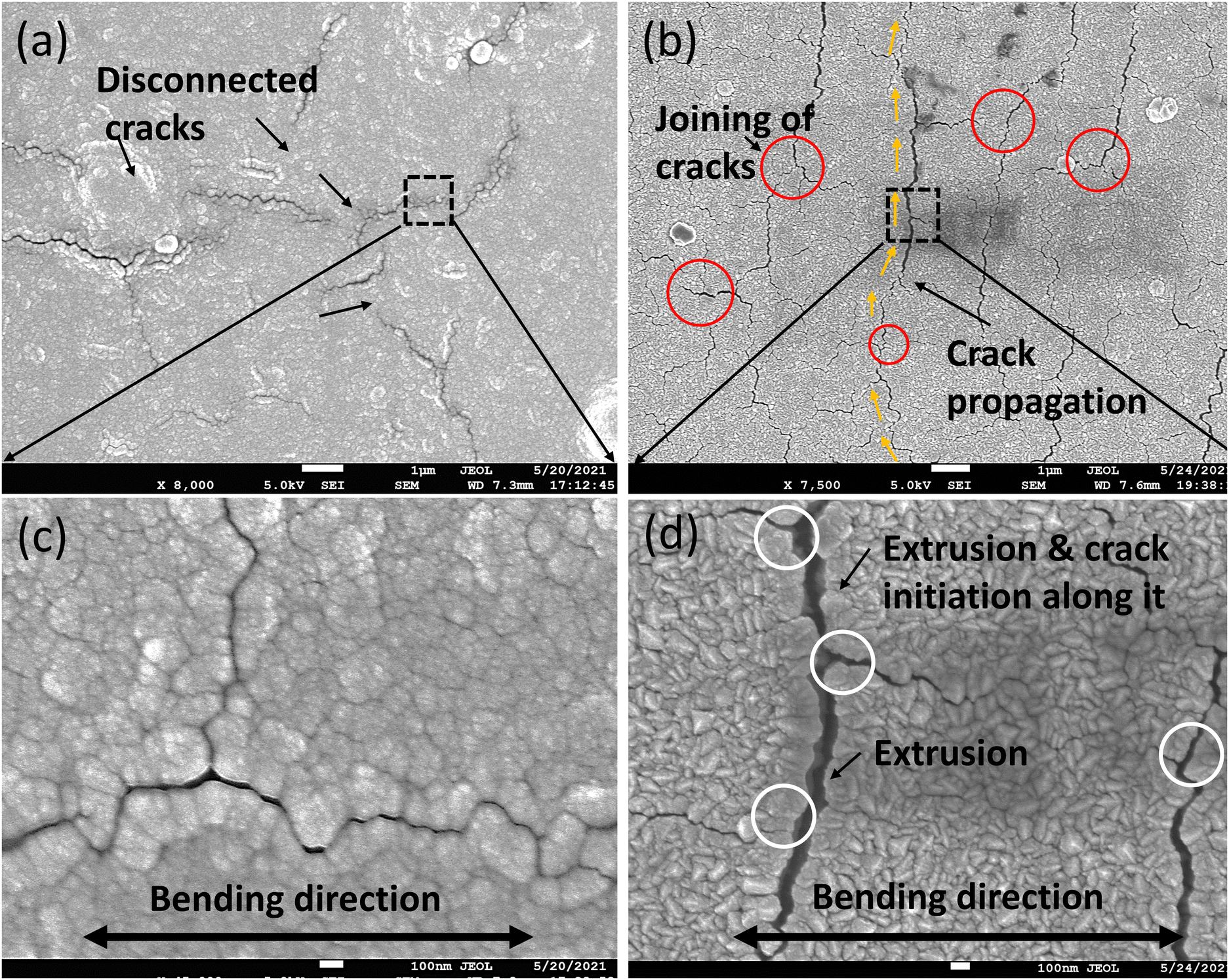 | ||
| Fig. 4 SEM micrographs of the samples after rate-dependent bending failure/fracture tests for (a and c) Ni–Nb2O5–PI. The surface cracks were discontinuous in nature with the no apparent presence of extrusions and (b and d) Ni–PI. Figures show the creation of surface extrusions, and then crack initiation along the extrusions. Cracks are predominantly perpendicular to the applied stress, i.e., to the bending direction especially for Ni–PI obtained in the major damage zone, also shown schematically in Fig. 1(b). These images were used for the calculation of surface crack density per 10 μm2 and crack dimensions (see Fig. S9, in ESI†). | ||
For a flexible device, the number of repeated bending cycles it can sustain before losing conductivity determines its operating life. Therefore, the aim of performing the rate-dependent bending failure/fracture test was to investigate how well the samples age over time i.e., how well the samples maintain their reliability over time. During the rate-dependent bending failure/fracture test, small imperfections or defects can initiate a crack. These imperfections/defects could be pre-existing or generated under the action of external stress. Later, crack growth could occur under the continued loading of the material during the test, which can be the main contributor to the failure of the material. As can be seen in Fig. 3, apart from the initial resistance oscillations and some intermittent resistance oscillations, the trend of ΔR/R% plateaus becomes more or less constant over time, especially for Ni–Nb2O5–PI, which signifies that the Ni–Nb2O5–PI ages well compared to Ni–PI over 0.5 million cycles. We believe that the highly compliant polyimide substrate and the insertion of Nb2O5 into the Ni nanolayers improve the reliability of the sample and this effect has been commonly observed for metal/metal nanolayers deposited on polymer substrates.45 It is worth noting that while the initial resistance and ΔR/R% are slightly higher for Ni–Nb2O5–PI than for Ni–PI due to the crystalline–amorphous interface, conductive behavior of 400 nm Ni on the PI substrate and inherent low conductivity of Nb2O5 as well as the low weight fraction of Ni, nevertheless, the crystalline–amorphous Ni–Nb2O5–PI nanolayers improve the operational reliability of the flexible device by having low resistance oscillations (amplitude) compared to Ni nanolayers, which is essential for robust electrical performance of the flexible devices.
Discussion
We investigated the Ni–Nb2O5–PI and Ni–PI samples via scanning electron microscopy (SEM) after the rate-dependent bending failure/fracture tests (see Fig. 3). Also, the cross-sectional SEM images of the samples (see ESI,† Fig. S6) confirmed the presence of columnar grains in both samples. For Ni–Nb2O5–PI, the average length of the grains along the horizontal direction is roughly identical to the thickness of the nanolayer (∼20 nm) (equiaxed). The cracks generated in the nanolayers are regarded as the leading cause of conductivity loss. The cracks occur in the upper damage area (see Fig. 1), which is shown in Fig. 4 for both samples. Typically, in the literature, as the layer thickness and the grain size reduce to ∼1–∼3 μm, extrusions become rarer, and for further smaller layer thicknesses and grain sizes amongst ∼1 μm to 100 nm, discrete dislocations are only noted and extrusions are practically repressed and exchanged by cracks laterally along the grain boundaries at the submicron scale61,62 (also seen in the cross-sectional TEM micrographs discussed later). In the present experiments, the total nanolayer thickness is ∼400 nm with ∼20 nm layer thickness for Ni–Nb2O5–PI. In the present case, the formation of extrusions is reduced but not absent, as seen in Fig. 4(d) for Ni–PI. In the case of face-centered-cubic (FCC) Ni, the initiation/propagation of cracks are related to cyclic strain localization leading to the creation of surface extrusions and then crack initiation along the extrusions causing a gradual decrease in fatigue/fracture strength of the sample (Ni–PI).62 On the other hand, for Ni–Nb2O5–PI, crystalline–amorphous interfaces and their related interfacial plasticity restrict the movement of dislocations or flow of shear bands and therefore cracks, leading to cracks that tend to be disconnected in nature, thus providing improved fatigue/fracture strength with possibly appreciable ductility (discussed in detail in the subsequent paragraphs related to the TEM analysis).The surface crack density per 10 μm2 for Ni–Nb2O5–PI and Ni–PI was ∼34 and ∼111, respectively. The crack dimensions are 1.20 ± 0.69 μm (min ∼0.30 μm and max ∼3.37 μm) and 0.76 ± 0.61 μm (min ∼0.22 μm and max ∼3.88 μm) for Ni–Nb2O5–PI and Ni–PI, respectively (see Fig. S9 in the ESI† and Table 1). The large surface crack density of Ni–PI is considered responsible for the severe oscillation of its ΔR/R% (see Fig. 3). In the case of Ni–PI, the crack propagation is relatively perpendicular to the direction of the applied stress, i.e., the bending direction, during rate-dependent bending failure/fracture tests. Nevertheless, the mean surface crack length is higher for Ni–Nb2O5–PI (1.20 μm) compared to Ni–PI (0.76 μm). Therefore, in order to supplement the surface crack analysis, cross-sectional TEM analyses of the samples were performed after the rate-dependent bending failure/fracture test.
TEM analysis is performed to analyze the fracture behavior of the nanolayers after rate-dependent bending failure/fracture tests as shown in Fig. 5 to 8. In the Ni–Nb2O5–PI sample, due to the high interfacial area/volume ratio, the interfaces play a vital role in defining its final properties. In the case of crystalline–amorphous nanolayers, the interfaces could absorb dislocations or block dislocations/shear band propagation. In addition, interfacial sliding may occur, which could improve the mechanical properties (strength and ductility) of the nanolayers and provide hindrance to the flow of cracks.52,53 TEM cross-sectional analysis of the sample after rate-dependent bending failure/fracture tests shows no interfacial delamination at the crystalline–amorphous interfaces. Furthermore, no thickness variation of the layers in Ni–Nb2O5–PI was observed after the tests. The TEM micrographs also confirm the expected thickness of 400 nm single layer Ni on PI and formation of 400 nm sandwich Ni–Nb2O5–PI (20 nm nickel (10 layers) and ∼20 nm niobium oxide (10 layers)) (see Fig. S6, ESI†). As expected, it is clear from the TEM micrographs (Fig. 5), that it is easier for the crack to nucleate and propagate vertically through the crystalline Ni–PI compared to Ni–Nb2O5–PI as there is no obstruction to the flow of dislocations (2 cracks through the thickness of the Ni–PI sample, typically along the grain boundary, see Fig. 5(c)). On the other hand, for Ni–Nb2O5–PI, the crystalline–amorphous interface obstructs the movement of dislocations or flow of shear bands and therefore, no catastrophic cracks were visible in Fig. 5(a and b).
 | ||
| Fig. 5 TEM cross-sectional micrographs of (a and b) Ni–Nb2O5–PI and (c and d) Ni–PI. For Ni–PI, it is easier for the crack to nucleate and propagate through the thickness compared to Ni–Nb2O5–PI, where interface obstructs the flow of dislocations thereby avoiding catastrophic failure. | ||
 | ||
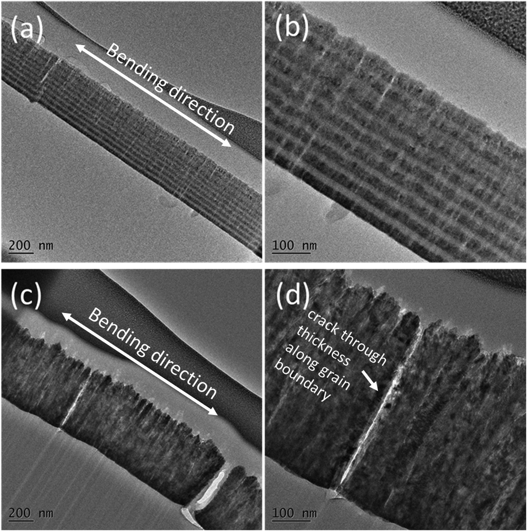
| Fig. 6 TEM cross-sectional micrographs with increasing magnification from (a–c) of Ni–PI showing the creation of cracks along the grain boundary originating from the substrate (PI). | ||
 | ||
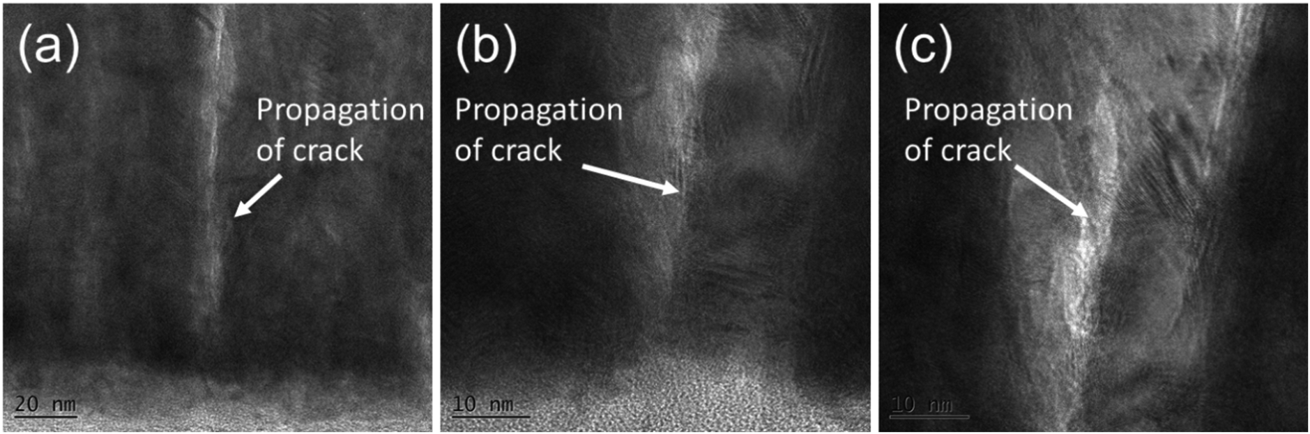
| Fig. 7 TEM cross-sectional micrographs of Ni–Nb2O5–PI showing (a) the motion of cracks and its diversions at the crystalline–amorphous interface due to interfacial sliding and (b) strong shear localization across the crystalline and amorphous layers due to alignment of slip plane in the crystalline layer with the shear band in the amorphous layer. | ||
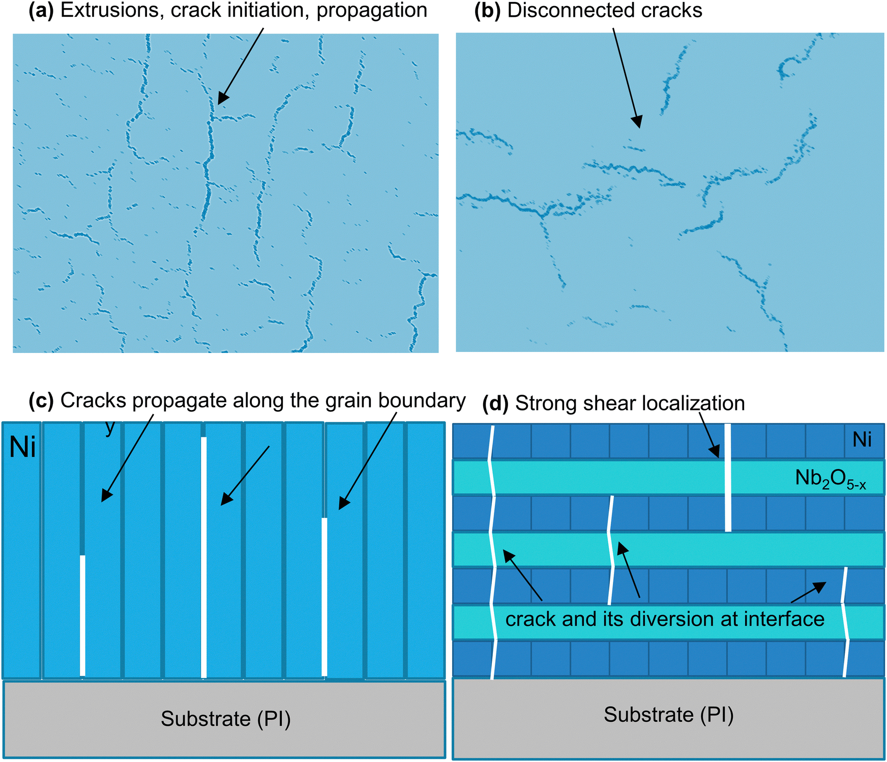 | ||
| Fig. 8 Schematic of the top view and cross-section of the sample after rate-dependent bending failure/fracture tests for (a and c) Ni–PI and (b and d) Ni–Nb2O5–PI. Crystalline–amorphous interface in Ni–Nb2O5–PI impedes the movement of dislocations or flow of shear bands as can be seen by disconnected cracks in the top view (b) and diversion of the cracks at the interface in the cross-sectional view (d), whereas in the crystalline Ni–PI, the cracks nucleate and propagate through the thickness as documented by extrusions and micro-cracks in the top view (a) and cracks through the thickness causing catastrophic failure in the cross-sectional view (c). | ||
Deng et al.63 through MD simulations, noted that the atomic structure of the crystalline–amorphous interface is mainly the result of inter-diffusion across the interface, which revealed no strong reliance on the crystallographic orientation of the crystalline nanolayer, unlike free surfaces and grain boundaries in predominantly crystalline materials. Nevertheless, the yielding/plasticity of crystalline–amorphous nanolayers depend on the actuated slip systems in the crystalline layer. For instance, once a certain slip plane in the crystalline nanolayer is aligned with a shear band in the amorphous nanolayer, robust shear localization through the crystalline–amorphous interface can be generated, as can be seen in Fig. 7(b). Moreover, at a few locations, the crack propagation is not parallel to the grain boundary as is the case for Ni–PI (see Fig. 5(c and d)); in Fig. 7(a), crack appears to have changed direction at the interface. This phenomenon is attributed to the crystalline–amorphous interface where shear bands are formed in the amorphous layer, accompanied by plastic deformation (flow of the dislocation) in the crystalline layer and their alignment is restricted due to interfacial sliding. The crystalline–amorphous interfaces mitigate the occurrence of catastrophic cracks, which was a common occurrence for nickel/PI (see Fig. 5(c and d) and 6).
Conclusions
Novel Ni–Nb2O5–PI sandwich crystalline–amorphous layers were fabricated and their electro-mechanical reliability as a flexible substrate (with electrode) for flexible electronic devices was investigated through a series of carefully executed nanoscale characterization tools and techniques. Our analysis clearly shows that the Nb2O5 layers in the Ni–Nb2O5–PI nanolayers create a crystalline–amorphous interface that impedes the movement of dislocations or flow of shear bands, thereby preventing the initiation/propagation of cracks and increasing the overall fracture/failure strength of the device (see Fig. 8). A tailored rate-dependent bending failure/fracture test system is used to study the electrical performance of the samples under repeated cyclic loading. The Ni–Nb2O5–PI sample has a slightly higher ΔR/R% than Ni–PI due to the high density of crystalline–amorphous interfaces and the inherently low conductivity of Nb2O5 and reduced weight fraction of Ni compared to Ni–PI. Furthermore, the electrical resistance of metallic Ni–PI can be considered to be roughly independent of the applied stress/stain during rate-dependent bending failure/fracture test because the single 400 nm Ni layer on PI (without any interface) provides several available electrical paths for the flow of current. Nevertheless, Ni–Nb2O5–PI samples displayed appreciably low resistance oscillations compared to Ni–PI, which is essential for operational reliability and robustness of the flexible device. These results suggest that a compromise amongst the electrical and mechanical properties of nanolayer-based flexible devices could certainly be achieved by careful tailoring of the nanolayer stack thickness, interface plasticity, conductivity, and microstructure. The layer thickness/composition (here, 20 nanometers, amorphous layers) of the inserted material in the otherwise crystalline nanolayers could be optimized according to the application of the flexible devices, which will be the focus of our future work. This inserted material layer thickness/composition, if carefully selected, would ensure appreciable fracture/failure resistance (with or without ductility), while minimizing the degradation/oscillation of electrical conductivity.Data availability statement
The data that support the findings of this study are available from the corresponding author upon a reasonable request.Author contributions
R. S.: conceptualization, methodology, investigation, visualization, validation, data collection, data analysis, writing – original draft, writing – review and editing, and supervision. Y. C. T.: visualization, data collection, and data analysis. I. A.: sample preparation, data collection, data analysis, and focused ion beam (FIB) and TEM analyses. A. S. B.: conceptualization, funding acquisition, methodology, investigation, writing – review and editing, and supervision. C. M. T.: supervision, writing – review and editing. P. S. L.: supervision, writing–review and editing. O. T.: supervision, writing – review and editing. N. R.: funding acquisition, methodology, investigation, writing – review and editing, and supervision. All the authors have read and agreed to the published version of the manuscript.Conflicts of interest
The authors declare no conflicts of interest.Acknowledgements
We gratefully acknowledge co-funding provided by the National Research Foundation (NRF), Singapore through the Grant NRF2018-NRF-ANR042 (Street Art Nano) and the ANR (Agence Nationale de la Recherche) of the French government through the Grant ANR ANR18-CE09-003801 (Street Art Nano). The corresponding author (Nagarajan Raghavan) would also like to acknowledge the support of the research surplus funding from Singapore University of Technology and Design (SUTD) under grant no. RS-INSUR-00019-E0601-S00 for Open Access article publication fee charges. ASB gratefully acknowledges the Oregon Renewable Energy Center (OREC)'s support and resources provided through the Grant OREC/WIND titled “Novel Materials Coating for Wind Turbine Blades Protection and Deicing” at OregonTech. RS, ASB and NR also acknowledge support from the eASIA JRP (Joint Research Program) Materials Informatics 2021, via JST SICORP JPMJSC21E1, Japan, titled “Data-Driven Design of Mechanical properties in Metallic Layered Structures”.References
- M. Kaltenbrunner, T. Sekitani, J. Reeder, T. Yokota, K. Kuribara, T. Tokuhara, M. Drack, R. Schwödiauer, I. Graz and S. Bauer-Gogonea, Nature, 2013, 499, 458–463 CrossRef CAS PubMed.
- S.-I. Park, Y. Xiong, R.-H. Kim, P. Elvikis, M. Meitl, D.-H. Kim, J. Wu, J. Yoon, C.-J. Yu and Z. Liu, Science, 2009, 325, 977–981 CrossRef CAS PubMed.
- T. Sekitani, H. Nakajima, H. Maeda, T. Fukushima, T. Aida, K. Hata and T. Someya, Nat. Mater., 2009, 8, 494–499 CrossRef CAS PubMed.
- J. Xiong, S. Li, J. Ciou, J. Chen, D. Gao, J. Wang and P. S. Lee, Adv. Funct. Mater., 2021, 31, 2006120 CrossRef CAS.
- W. S. Wong and A. Salleo, Flexible electronics: materials and applications, Springer Science & Business Media, 2009, vol. 11 Search PubMed.
- P.-C. Kuo, V. G. Chouvardas, J. A. Spirko, K. M. Hatalis and M. K. Hatalis, MRS Online Proc. Libr., 2007, 1030, 1–6 Search PubMed.
- T. Rachow, S. Reber, S. Janz, M. Knapp and N. Milenkovic, Energy Sci. Eng., 2016, 4, 344–351 CrossRef CAS.
- Y. H. Jung, T.-H. Chang, H. Zhang, C. Yao, Q. Zheng, V. W. Yang, H. Mi, M. Kim, S. J. Cho and D.-W. Park, Nat. Commun., 2015, 6, 1–11 Search PubMed.
- E. Lay, D.-S. Wuu, S.-Y. Lo, R.-H. Horng, H.-F. Wei, L.-Y. Jiang, H.-U. Lee and Y.-Y. Chang, Surf. Coat. Technol., 2011, 205, 4267–4273 CrossRef CAS.
- X. Chen, X. Han and Q. Shen, Adv. Electron. Mater., 2017, 3, 1600460 CrossRef.
- M. Melzer, J. I. Mönch, D. Makarov, Y. Zabila, G. S. Cañón Bermúdez, D. Karnaushenko, S. Baunack, F. Bahr, C. Yan and M. Kaltenbrunner, Adv. Mater., 2015, 27, 1274–1280 CrossRef CAS PubMed.
- V. Zardetto, T. M. Brown, A. Reale and A. Di Carlo, J. Polym. Sci. B Polym. Phys., 2011, 49, 638–648 CrossRef CAS.
- D. Qi, K. Zhang, G. Tian, B. Jiang and Y. Huang, Adv. Mater., 2021, 33, 2003155 CrossRef CAS PubMed.
- X. Liu, Y.-Z. Long, L. Liao, X. Duan and Z. Fan, ACS Nano, 2012, 6, 1888–1900 CrossRef CAS PubMed.
- Q.-H. Lu and F. Zheng, Advanced Polyimide Materials, Elsevier, 2018, pp. 195–255 Search PubMed.
- D. Gao, J. Lv and P. S. Lee, Adv. Mater., 2021, 2105020 Search PubMed.
- P. Lee, J. Lee, H. Lee, J. Yeo, S. Hong, K. H. Nam, D. Lee, S. S. Lee and S. H. Ko, Adv. Mater., 2012, 24, 3326–3332 CrossRef CAS PubMed.
- A. Khalajhedayati, Z. Pan and T. J. Rupert, Nat. Commun., 2016, 7, 1–8 Search PubMed.
- H. Bark and P. S. Lee, Chem. Sci., 2021, 12, 2760–2777 RSC.
- J. Lee, M. W. M. Tan, K. Parida, G. Thangavel, S. A. Park, T. Park and P. S. Lee, Adv. Mater., 2020, 32, 1906679 CrossRef CAS PubMed.
- W. Guo, E. Jägle, J. Yao, V. Maier, S. Korte-Kerzel, J. M. Schneider and D. Raabe, Acta Mater., 2014, 80, 94–106 CrossRef CAS.
- M. C. Liu, X. H. Du, I. C. Lin, H. J. Pei and J. C. Huang, Intermetallics, 2012, 30, 30–34 CrossRef.
- Y. Wang, J. Li, A. V. Hamza and T. W. Barbee, Proc. Natl. Acad. Sci. U. S. A., 2007, 104, 11155–11160 CrossRef CAS PubMed.
- H. P. A. Ali, I. Radchenko, N. Li and A. Budiman, J. Mater. Res., 2019, 34, 1564–1573 CrossRef.
- H. Huang and F. Spaepen, Acta Mater., 2000, 48, 3261–3269 CrossRef CAS.
- N. Li, H. Wang, A. Misra and J. Wang, Sci. Rep., 2014, 4, 1–6 Search PubMed.
- S. K. Tippabhotla, N. G. Diesta, X. Zhang, S. Sridhara, C. V. Stan, N. Tamura, A. A. O. Tay and A. S. Budiman, Sol. Energy Mater. Sol. Cells, 2019, 193, 387–402 CrossRef CAS.
- S. K. Tippabhotla, W. J. R. Song, A. A. O. Tay and A. S. Budiman, Sol. Energy, 2019, 182, 134–147 CrossRef CAS.
- T. Nizolek, I. J. Beyerlein, N. A. Mara, J. T. Avallone and T. M. Pollock, Appl. Phys. Lett., 2016, 108, 2–6 CrossRef.
- Z. Pan and T. J. Rupert, Acta Mater., 2015, 89, 205–214 CrossRef CAS.
- B. Cheng and J. R. Trelewicz, Acta Mater., 2016, 117, 293–305 CrossRef CAS.
- G. Hakansson, J. Sundgren, D. Mcintyre, J. E. Greene and W. MiiNZ, N. B. Alloys Grown Dc Magnetron Sputter Deposition, Leybold-Heraeus GmbH, 55 Microstructure And Physical Properties Of Polycrystalline Metastable Ti, 1987, vol. 153 Search PubMed.
- S. Takeda, S. Suzuki, H. Odaka and H. Hosono, Photocatalytic TiO thin film deposited onto glass by DC 2 magnetron sputtering, 2001, vol. 392 Search PubMed.
- O. Wilhelmsson, J. P. Palmquist, E. Lewin, J. Emmerlich, P. Eklund, P. O. Å. Persson, H. Högberg, S. Li, R. Ahuja, O. Eriksson, L. Hultman and U. Jansson, J. Cryst. Growth., 2006, 291, 290–300 CrossRef CAS.
- J. T. Gudmundsson, Plasma Sources Sci. Technol., 2020, 29 Search PubMed.
- J. Musil, Recent advances in magnetron sputtering technology, 1998, vol. 1 Search PubMed.
- S. Takeda, S. Suzuki, H. Odaka and H. Hosono, Photocatalytic TiO thin film deposited onto glass by DC 2 magnetron sputtering, 2001, vol. 392 Search PubMed.
- W. Posadowski, A. Wiatrowski and G. Kapka, Mater. Sci., 2018, 36, 69–74 CAS.
- G. Ramírez, S. E. Rodil, S. Muhl, D. Turcio-Ortega, J. J. Olaya, M. Rivera, E. Camps and L. Escobar-Alarcón, J. Non Cryst. Solids, 2010, 356, 2714–2721 CrossRef.
- A. Mallikarjuna Reddy, A. Sivasankar Reddy and P. Sreedhara Reddy, Vacuum, 2011, 85, 949–954 CrossRef CAS.
- J. Keraudy, J. García Molleja, A. Ferrec, B. Corraze, M. Richard-Plouet, A. Goullet and P. Y. Jouan, Appl. Surf. Sci., 2015, 357, 838–844 CrossRef CAS.
- M. P. F. Graça, M. Saraiva, F. N. A. Freire, M. A. Valente and L. C. Costa, Thin Solid Films, 2015, 585, 95–99 CrossRef.
- H. P. Anwar Ali and A. Budiman, J. Mater. Res., 2019, 34, 1449–1468 CrossRef CAS.
- S.-S. Hwang, S.-Y. Jung and Y.-C. Joo, J. Appl. Phys., 2008, 104, 44511 CrossRef.
- S.-M. Yi, I.-S. Choi, B.-J. Kim and Y.-C. Joo, Elec. Mater. Lett., 2018, 14, 387–404 CrossRef CAS.
- K. Kato, Y. Hatasako, M. Kashiwagi, H. Hagino, C. Adachi and K. Miyazaki, J. Electron. Mater., 2014, 43, 1733–1739 CrossRef CAS.
- H. P. A. Ali, I. Radchenko, N. Li and A. Budiman, J. Mater. Sci. Eng. A, 2018, 738, 253–263 CrossRef.
- A. S. Budiman, R. Sahay, H. P. A. Ali, S. K. Tippabhotla, I. Radchenko and N. Raghavan, J. Mater. Sci. Eng. A, 2020, 140705 Search PubMed.
- I. Radchenko, H. P. Anwarali, S. K. Tippabhotla and A. S. Budiman, Acta Mater., 2018, 156, 125–135 CrossRef CAS.
- R. Shivakumar, S. K. Tippabhotla, V. A. Handara, G. Illya, A. A. O. Tay, F. Novoa, R. H. Dauskardt and A. S. Budiman, Procedia Eng., 2016, 139, 47–55 CrossRef.
- S. L. Fernandes, L. G. S. Albano, L. J. Affonço, J. H. D. da Silva, E. Longo and C. F. de O. Graeff, Front. Chem., 2019, 7, 50 CrossRef CAS PubMed.
- T. G. Nieh and J. Wadsworth, Intermetallics, 2008, 16, 1156–1159 CrossRef CAS.
- J. Y. Zhang, G. Liu, S. Y. Lei, J. J. Niu and J. Sun, Acta Mater., 2012, 60, 7183–7196 CrossRef CAS.
- S. P. Baker and W. D. Nix, Optical Thin Films III: New Developments, International Society for Optics and Photonics, 1990, vol. 1323, pp. 263–276 Search PubMed.
- G. Feng, A. S. Budiman, W. D. Nix, N. Tamura and J. R. Patel, J. Appl. Phys., 2008, 104, 43501 CrossRef.
- S. M. Han, R. Saha and W. D. Nix, Acta Mater., 2006, 54, 1571–1581 CrossRef CAS.
- W. A. Spitzig, A. R. Pelton and F. C. Laabs, Acta Metall., 1987, 35, 2427–2442 CrossRef CAS.
- N. Hossain, O. Günes, C. Zhang, C. Koughia, Y. Li, S.-J. Wen, R. Wong, S. Kasap and Q. Yang, J. Mater. Sci.: Mater. Electron., 2019, 30, 9822–9835 CrossRef CAS.
- C. Nico, T. Monteiro and M. P. F. Graça, Prog. Mater. Sci., 2016, 80, 1–37 CrossRef CAS.
- J. Guénolé, J. Godet and S. Brochard, Phys. Rev. B: Condens. Matter Mater. Phys., 2013, 87, 45201 CrossRef.
- D. Wang, P. A. Gruber, C. A. Volkert and O. Kraft, J. Mater. Sci. Eng. A, 2014, 610, 33–38 CrossRef CAS.
- G. P. Zhang, C. A. Volkert, R. Schwaiger, P. Wellner, E. Arzt and O. Kraft, Acta Mater., 2006, 54, 3127–3139 CrossRef CAS.
- E. Alishahi and C. Deng, Comput. Mater. Sci., 2018, 141, 375–387 CrossRef CAS.
Footnote |
| † Electronic supplementary information (ESI) available. See DOI: https://doi.org/10.1039/d3ma00147d |
| This journal is © The Royal Society of Chemistry 2023 |