DOI:
10.1039/D2MA00911K
(Paper)
Mater. Adv., 2023,
4, 215-222
Improved electrical conductivity of Co(II) and Cu(II) ladder polymers in the fabrication of photoresponsive Schottky devices†
Received
19th September 2022
, Accepted 9th November 2022
First published on 10th November 2022
Abstract
In this work, two new Cu(II) and Co(II) based coordination polymers (CPs), [Co2(bpd)2(nac)2]·2CH3OH·H2O (Co-CP) and [Cu2(bpd)2(nac)2]·2CH3CN·2H2O (Cu-CP) respectively, have been synthesized using a bidentate pyridyl ligand, N,N′-bis(1-pyridine-4-yl-ethylidene) (bpd), linker with the less explored 3-(1-naphthyl)acrylic acid (nac) ligand appended at the metal centre to fulfil the molecular geometry. Here, Co-CP forms a one-dimensional (1D) ladder polymer, whereas Cu-CP consists of a combination of 1D chains and 1D ladder polymers. Interestingly, both the CPs exhibit semiconducting behaviour with increased conductivity upon illumination, signifying the photosensitive nature. However, Cu-CP reveals better conductivity as compared to Co-CP. This is obvious from the field emission electron microscopy (FESEM) study, where Cu-CP with flower-like morphology shows a higher surface area with respect to the rod-shaped morphology of Co-CP, resulting in higher charge transport. To the best of our knowledge, Co/Cu based CPs showing photosensitivity seem to be scarce. Thus, this study opens a new avenue in the fabrication of photoresponsive electronic devices.
Introduction
The dramatic revolution of laboratory to land applications of materials chemistry propagates at an extraordinary pace. Application of materials has directly been governed by the structural architecture and morphology. In this regard, coordination polymers (CPs)1–9 have attracted materials researchers mostly because of their unique molecular structures and excellent stabilities. These hybrid molecular systems are constructed through inorganic metal ions or metal clusters and organic ligands.10–15 Hence, the molecular properties as well as applications are also regulated by the nature of the metal centers and ligands. A combination of organic components (O-donor and N-donor ligands) is commonly exploited to achieve structural varieties and desired molecular properties.16–18 In these coordination systems, metal salts or organic linkers are judiciously selected to confer the application field. In fact, there is an essential relationship between the structural architecture, properties and utilities of the materials. Rational construction and scientific judgment during the engineering of these crystalline materials make them easier to characterize and illustrate important structure–property relationships. In the construction of higher dimensional supramolecular architecture, various supramolecular interactions such as hydrogen bonding, π⋯π, C–H⋯π, cation⋯π, anion⋯π, halogen⋯halogen, halogen⋯π and van der Waals interactions play the crucial role.19–21 Sometimes, these self-assembled structures are entirely unlike and more proficient than the unassembled forms. The discussed inorganic–organic hybrid materials are extremely applicable in the territory of gas sorption, molecular storage and separation, ion exchange, electrochemical catalysis, energy technology, drug delivery, temperature-dependent magnetism, sensing and detection of noxious ions and emerging analytes, proton conductance, electrical conductivity, electronic device fabrication, etc.22–34
Of these, utilization of CPs in electrical conductivity and device fabrication is particularly important as these CPs can be explored to overcome the energy crisis situation and for technological interest. However, in CPs, the poor extended electronic coupling among the metal nodes and the ligands impedes competent charge transport.35–38 The consequential electronic bands display nominal dispersion, which indicates that the electrons are strongly localized over the whole lattice. The band dispersion determines the efficacy of the compound to transmit electrical current. Therefore, the crucial facet is to adjust the electronic connection among the metal centers and the organic ligands to enhance delocalization for higher conductivity.39–41 In this regard, a substantive number of CPs based on d10 metal ions (Zn2+/Cd2+) have been reported and those behave as semiconducting materials. Some of the materials have also exhibited photosensitivity properties, i.e. enhancement of conductivity upon illumination.37 However, varying metal ions in tailor-fit synthesis, we can easily regulate the semiconducting nature as well as the photosensitivity behavior of CPs. In this facet, CPs based on Co(II)/Cu(II) metal ions with semiconducting properties have not been much explored and remain more elusive in regard to photosensitivity.8,40
Herein, we report two Co(II) and Cu(II) based one-dimensional (1D) CPs [Co2(bpd)2(nac)2]·2CH3OH·H2O (Co-CP) and [Cu2(bpd)2(nac)2]·2CH3CN·2H2O (Cu-CP) which have been utilized to fabricate metal–semiconductor (MS) junction Schottky devices (SDs). The current–voltage (I–V) characteristics of the fabricated SDs were measured to estimate the diode parameters, such as on/off ratio, photosensitivity, ideality factor, barrier height, and series resistance. The study reveals that both the CPs exhibit higher charge conduction upon illumination signifying the photosensitive nature. The charge transport parameters including mobility and lifetime of the charge carriers were also investigated with the help of the space–charge limited current (SCLC) theory, which demonstrates the improved device performance of Co-CP and Cu-CP. However, Cu-CP exhibits better conductivity with respect to Co-CP. This observation is also supported by a field emission scanning electron microscope (FESEM) study. Flower-like morphology of Cu-CP offers higher surface area as compared to rod-shaped Co-CP and exhibits increased electrical conductivity.
Results and discussion
Structural description of [Co2(bpd)2(nac)2]·2CH3OH·H2O (Co-CP)
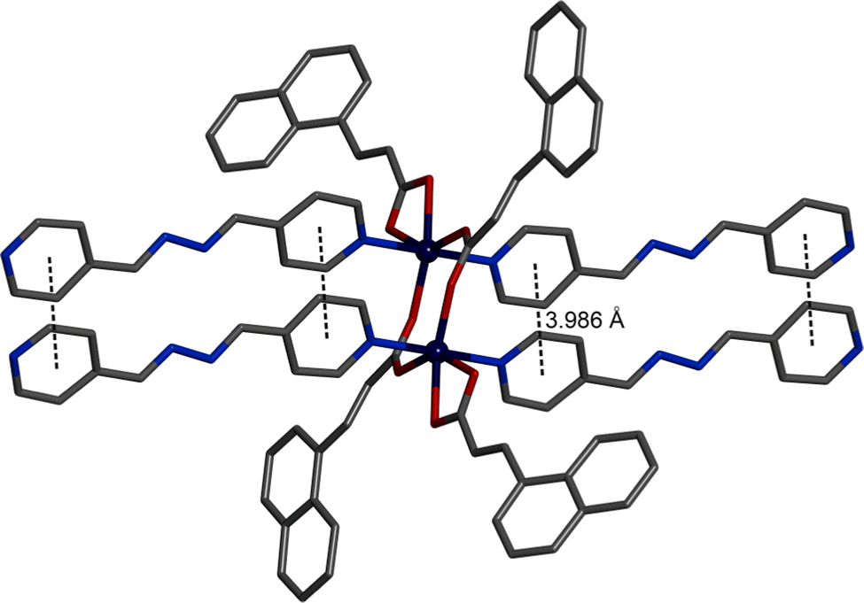
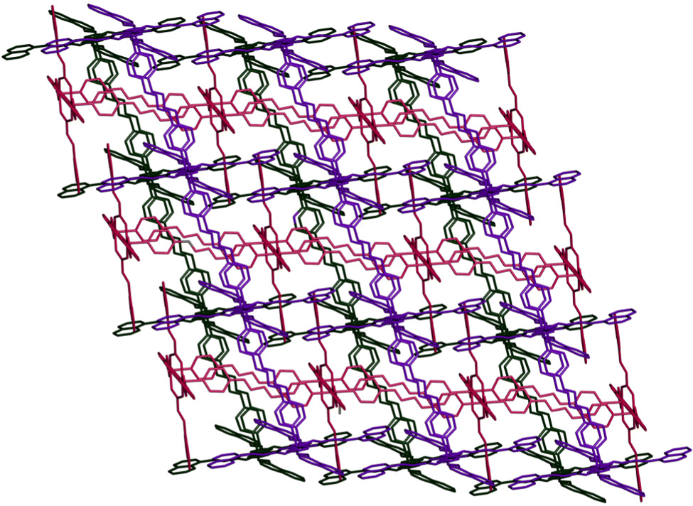
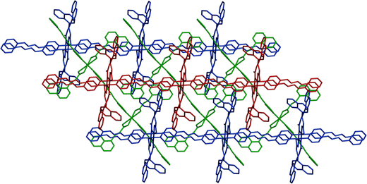
The single crystal X-ray diffraction (SCXRD) study reveals that Co-CP crystallizes in the monoclinic space group C2/c. The asymmetric unit consists of one Co(II) centre, two nac ligands and a bpd ligand. The asymmetric unit further contains one each of CH3OH and H2O molecules in the lattice (Fig. S1, ESI†). The Co(II) centre adopts a six-coordinated octahedral geometry (Fig. 1). The equatorial plane is defined by two O atoms of a chelating nac ligand and two O atoms of two bridging nac ligands. To complete the octahedron, two N atoms from two bpd ligands take the axial positions. Here also, two Co(II) centres and two bridging carboxylate groups form a dinuclear 8-membered [Cu2(O2CC)2] secondary building unit (SBU) with Co⋯Co distance of 4.3064 Å. Thereby, a pair of bpd ligands are aligned parallel via π⋯π stacking contacts with the centroid–centroid distance of 3.986 Å (Fig. 1). A crystallographic inversion centre is also found in the middle of the ring. The SBUs and a pair of bpd ligands are combined to generate a 1D ladder polymer. Further, the 1D ladder polymers undergo extensive π⋯π stacking interactions with the centroid–centroid distance of 3.766–3.849 Å to form a 3D supramolecular assembly. In the solid-state structure, if the π⋯π interactions are considered as joining the ladder polymers, they would generate a 2D layer structure. The aligned bpd pairs act as pillars which join the 2D layers into a doubly interpenetrated 3D supramolecular pillar-layered network of cubic topology (Fig. 2 and Fig. S2, ESI†).
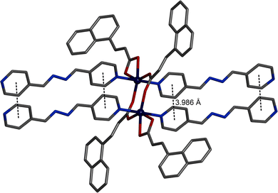 |
| | Fig. 1 Dimeric SBU of Co-CP with coordination environment around Co(II) centres. Carbon: gray; nitrogen: blue; oxygen: red; cobalt: navy. Hydrogen atoms and solvent molecules are not shown for clarity. Dashed lines represent the π⋯π contacts between bpd ligands. | |
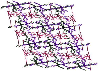 |
| | Fig. 2 Doubly interpenetrated 3D supramolecular pillar-layered structure of Co-CP. | |
Structural description of [Cu2(bpd)2(nac)2]·2CH3CN·2H2O (Cu-CP)
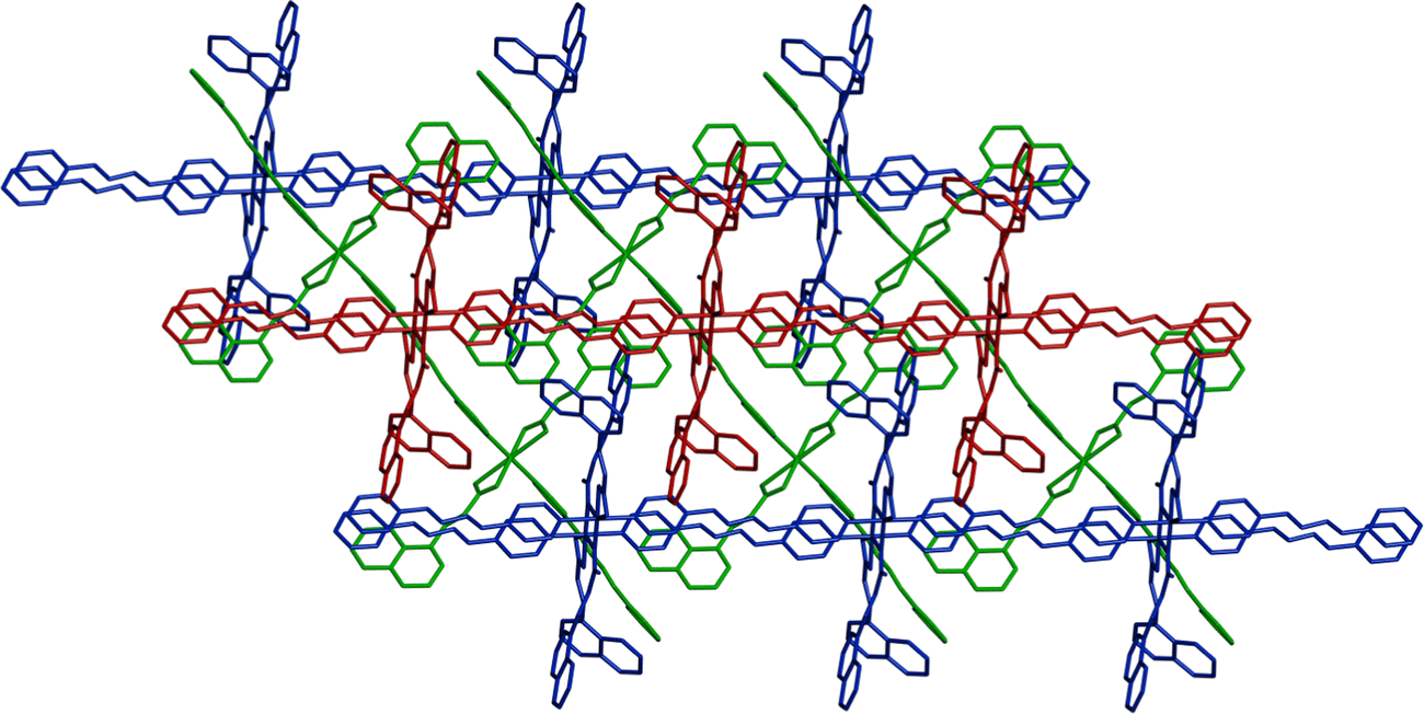
The SCXRD study reveals that Cu-CP also crystallizes in the monoclinic space group C2/c. The asymmetric unit contains two parts (Fig. S3, ESI†). The first part consists of a Cu(II) centre (Cu1), one bpd ligand and two nac ligands. However, the second part comprises a Cu(II) centre (Cu2), half a bpd ligand and one nac ligand. The asymmetric unit further consists of one each of CH3CN and H2O molecules in the lattice (Fig. S3, ESI†). All the Cu(II) centres adopt six-coordinated octahedral geometries (Fig. 3). The equatorial plane of the octahedron is formed by two O atoms from a chelating nac ligand and two O atoms from two nac ligands. Two N atoms of two bpd ligands occupy the axial positions. Here, two Cu(II) centres and bridging carboxylate groups form a 8-membered dinuclear [Cu2(O2CC)2] secondary building unit (SBU) with Cu⋯Cu distance of 3.4843(6) Å. A pair of bpd ligands are aligned via face-to-face π⋯π stacking interactions (centroid–centroid distance 3.776 Å) (Fig. 3). A crystallographic inversion centre is present in the middle of the [Cu2(O2CC)2] ring. A 1D ladder polymer is obtained by the combination of SBUs and a pair of bpd ligands (Fig. 4).
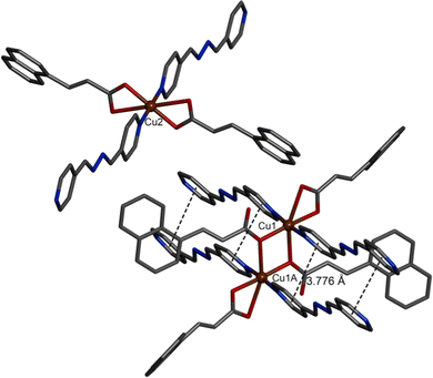 |
| | Fig. 3 Coordination environment around Cu(II) centres of Cu-CP. Carbon: gray; nitrogen: blue; oxygen: red; copper: brown. Hydrogen atoms and solvent molecules are not shown for clarity. Dashed lines represent the π⋯π stacking interactions between bpd ligands. | |
 |
| | Fig. 4 The 3D supramolecular network of Cu-CP comprising 1D ladder polymers and 1D linear chains. | |
On the other hand, the Cu2 centre is surrounded by four O atoms of two carboxylate groups from two individual chelating nac ligands forming the equatorial plane, while two N atoms from two individual bpd ligands complete the octahedral geometry. The connectivity of the Cu2 centre and nac ligand leads to the formation of a 1D linear chain. Further, 1D ladder polymers and 1D linear chains are assembled to form 3D supramolecular frameworks by the arrangement of extensive face-to-face π⋯π stacking interactions (centroid–centroid distance 3.834 Å), and C–H⋯π interactions with edge-to-face distance of 3.023–3.160 Å (Fig. 4 and Fig. S4, ESI†).
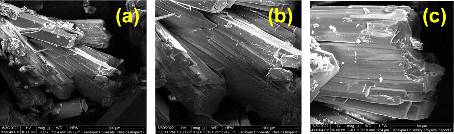
Surface morphological studies
The surface morphologies of the Co-CP and Cu-CP were investigated using FESEM micrographs and are displayed in Fig. 5 and 6. These kinds of microstructures of the polymers not only help to study shapes and sizes, but also show the characteristics of the MS junction that is formed while fabricating the Schottky diodes. It is observed from the images that the Co-CP are rod-shaped (Fig. 5), while the Cu-CP are flower-like (Fig. 6). The flower-like shapes offer higher surface area, contributing to the higher contact area and larger electrical conduction.42 This study prompts us to investigate further the electrical conductivity of the materials.
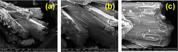 |
| | Fig. 5 FESEM micrographs of Co-CP. | |
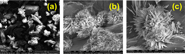 |
| | Fig. 6 FESEM micrographs of Cu-CP. | |
Optical properties
The optical spectra of Co-CP and Cu-CP were recorded to estimate their optical band gaps. To deduce the band gaps, Tauc's equation (eqn (1))43 was employed, which is given by:where α is the absorption coefficient, Eg is the bandgap, h is Planck's constant, ν is frequency, A is a constant, and n = 2 and 1/2 corresponding to the allowed direct and indirect optical transitions, respectively. By extrapolating the linear region of the plot (αhν)2vs. hν to α = 0, as displayed in Fig. S11 (ESI†), the direct optical band gaps of Co-CP and Cu-CP were evaluated as 3.48 eV and 3.46 eV respectively, which suggest the intermediate band gap region.31
Device fabrication method
To study the electrical characteristics of Co-CP and Cu-CP, the MS junction SDs based on these CPs were fabricated. In a typical method, first ITO-coated glass substrates were cleaned using acetone, followed by 2-propanol and distilled water. Then, on the top of the cleaned indium tin oxide (ITO) coated substrate, a thin film of Co-CP/Cu-CP was deposited by the spin coating unit. Subsequently, the as-prepared films were dried in a vacuum oven for 1 h. Next, as a metallic contact, aluminium (Al) was deposited onto the coated film using a vacuum coating unit (12A4D, HINDHIVAC) under an atmospheric pressure of 4.7 × 10⁻⁶ torr in the deposition method. In this process, a typical quad punch-hole shadow mask was used to control the effective diode area of the Schottky device as 7.065 × 10⁻⁶ m−2. The schematic diagram of the Al/CPs/ITO structure is portrayed in Scheme 1.
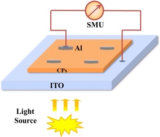 |
| | Scheme 1 Schematic diagram of the fabricated Al/CPs/ITO SDs. | |
Current–voltage (I–V) measurement
The electrical properties of the MS junction thin-film devices of Co-CP and Cu-CP were investigated. For this, the current–voltage (I–V) characteristics of the CP based Schottky devices were studied between the applied bias voltage of ±1 V under dark and light conditions. The I–V characteristics of the ITO/CPs/Al configurations presented in Fig. 7 exhibit a nonlinear rectifying behaviour for the SDs. The conductivities of the CPs under dark and light conditions were measured. It has been observed that the charge conduction is higher under illumination for both of the CPs, signifying the photo-responsive nature.
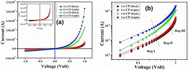 |
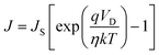
| | Fig. 7 (a) I–V characteristics curves for Co-CP and Cu-CP based devices. (b) I–V curves on logarithmic scale. | |
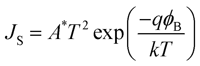
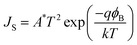
The current vs. voltage characteristics of the CP-based SDs were further discussed using thermionic emission (TE) theory.44 Here, the differential method first exploited by Cheung et al. was employed to evaluate different SD parameters.45 The current density (J) vs. voltage (V) curves could be written as:46
| |  | (2) |
where
q is the charge of the electron,
k is the Boltzmann constant,
T is the temperature,
VD is the potential drop and
η is the ideality factor
J and
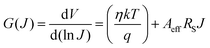
JS are respectively the current density and the current density at saturation, which is also given by:
| |  | (3) |
where
A* stands for the Richardson constant and
ϕB is the barrier height. Considering
VD =
V −
IRS using the Cheung and Cheung method,
47eqn (2) could be reduced to the following differential form:
| |  | (4) |
Furthermore, considering the function
H(
J) as
eqn (5), the barrier or potential height of the SDs was deduced using the following
eqn (6):
| |  | (5) |
The
G(
J)
vs. J and
H(
J)
vs. J graphs for dark and light conditions are presented in
Fig. 8(a–d) respectively. The ideality factor (
η) and series resistance (
RS) were determined from the intercept and slope of the linearly fitted plot of
G vs. J, respectively. On the other hand, the barrier heights (
ϕB) for the
Co-CP and
Cu-CP based devices are determined from the
H vs. J plot. The obtained values of the photosensitivity and the dc conductivity under dark and illumination conditions are listed in
Table 1, which depicts that
Cu-CP is more photo responsive than
Co-CP. Also,
Cu-CP exhibits higher conductivity as compared to
Co-CP.
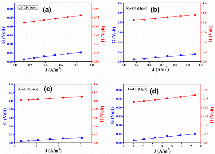 |
| | Fig. 8
G vs. J and H vs. J plots under dark and light conditions for (a and b) Co-CP, and (c and d) Cu-CP based thin-film devices. | |
Table 1 Charge transport parameters
|
|
Photosensitivity (S) |
Conductivity (σ) (S m−1) |
| Dark |
Light |
|
Co-CP
|
0.41 |
4.78 × 10⁻⁶ |
6.15 × 10⁻⁶ |
|
Cu-CP
|
0.86 |
19.97 × 10⁻⁶ |
70.61 × 10⁻⁶ |
The measured ideality factors (η), series resistances (RS) and barrier heights (ϕB) for Co-CP and Cu-CP under both dark and illumination conditions are listed in Table 2. It is observed that, after light soaking, the ideality factor of both of the CP-based devices approached very close to 1, indicating a more ideal device. This is generally due to the reduced photo-carrier recombination at the junction under light irradiation.43 In the presence of light, the series resistances were drastically reduced compared to the dark condition, causing a large increase in the photocurrent. The evaluated values of barrier height also show that under light, the turn-on voltages were slightly decreased. Table 2 manifests the improved diode behaviour for the Cu-CP based diodes. Also, the enhanced performance of both of the devices after light illumination portrays the excellent potential of Co-CP and Cu-CP in the field of various optoelectronic devices.
Table 2 Schottky diode parameters
|
|
Ideality factor (η) |
Barrier height (ϕB) (eV) |
Series resistance (RS) (kΩ) |
| Dark |
Light |
Dark |
Light |
Dark |
Light |
|
Co-CP
|
0.89 |
1.15 |
0.72 |
0.71 |
23.42 |
16.41 |
|
Cu-CP
|
1.43 |
1.01 |
0.70 |
0.66 |
4.21 |
2.60 |
The study of different diode parameters led us to thoroughly observe the charge transport properties of the CPs. In this regard, the I–V curves are plotted on the logarithmic scale (Fig. 7b). Fig. 7b reveals three distinguishable slopes, which are marked as region-I, II and III. In region-I, the current follows as I ∝ V, which denotes the ohmic region. In the second region, the slope is close to 2, where the current varies as I ∝ V2 and is controlled by the space–charge limited current (SCLC) field (Fig. 9).48 The injected carriers increase much higher as proportional to the background carriers. As a result, it spreads all over the space and creates a space–charge field. In region III, the injection level of electrons is much higher and they follow the power-law (I ∝ Vn, where n > 2).
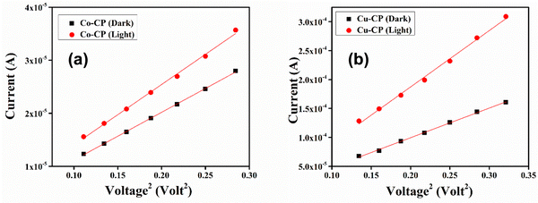 |
| | Fig. 9
I vs. V
2 curves under both dark and light conditions for (a) Co-CP and (b) Cu-CP based thin-film devices. | |
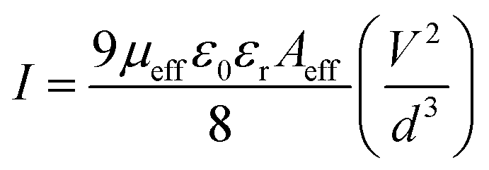
Following this model, the effective carrier mobility was deduced using the Mott–Gurney equation:49
| |  | (7) |
where
Aeff,
ε0,
εr and
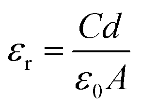
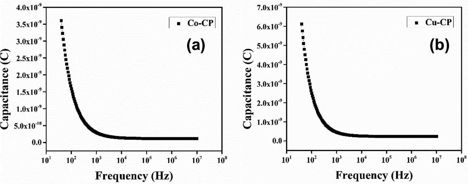
d are the effective diode area, the free space permittivity, the dielectric constant of the materials and the thickness of the diode, respectively. The dielectric constant (
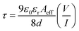
εr) was evaluated from the capacitance
vs. frequency plot (
Fig. 10) by employing the following equation:
50| |  | (8) |
where
C is the capacitance at saturation,
d is the thickness of the film,
A is the effective area and
ε0 is the permittivity of free space.
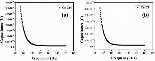 |
| | Fig. 10 Capacitance versus frequency (C–f) plots of (a) Co-CP and (b) Cu-CP. | |
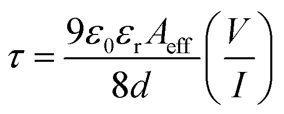
Transit time (τ), which is another key parameter to study charge transport across the SD junction,51 was evaluated using the following equation:
| |  | (9) |
All the deduced values of the diode parameters displayed that the charge conduction of the CPs was improved after light irradiation (
Table 3). Also, the higher conductivity (
Table 1) of
Cu-CP could be accredited to its higher mobility and lower transit or lifetime. It is also to be noted that the diode characteristics as well as the transport parameters of both the Co(
II) and Cu(
II) CP based SDs demonstrate much enhanced charge transfer properties after light soaking (Scheme S1, ESI
†). The transient photocurrent
vs. time measurements were performed to study the conducting mechanism of the CPs. It is observed that the conductivity of the CP does not vary with the passage of time (Fig. S12, ESI
†). Thus,
Co-CP and
Cu-CP display immense potential to be employed in photoresponsive device applications.
Table 3 SCLC parameters
|
|
ε
r
|
μ
eff (m2 V−1 s−1) |
τ (s) |
| Dark |
Light |
Dark |
Light |
|
Co-CP
|
1.15 × 10⁻¹⁰ |
6.94 × 10⁻⁷ |
8.72 × 10⁻⁷ |
1.66 × 10⁻⁶ |
1.31 × 10⁻⁶ |
|
Cu-CP
|
2.34 × 10⁻¹⁰ |
1.94 × 10⁻⁶ |
3.70 × 10⁻⁶ |
5.51 × 10⁻⁷ |
2.90 × 10⁻⁷ |
Conclusion
In summary, the present work analyses an unusual utilization of transition metal ions in the fabrication of CPs. Here, less explored nac acts as an ancillary ligand and bpd links the metal centres to generate 1D chains. The materials have been employed to fabricate semiconducting Schottky devices; through which electrical properties have been analyzed. Interestingly, the electrical conductivities of the materials have been enhanced upon light illumination. Therefore, the synthesized CPs can act as next generation photosensitive electronic materials. Charge transportation and electrical conductivity are also well tuned with the metal nodes present in the structural architecture. This work can be an inspiration for future researchers in the field of materials science.
Conflicts of interest
There are no conflicts to declare.
Acknowledgements
This work was supported by UGC-DAE CSR, India (Grant No. CRS/2021-22/02/538 Dated 30/03/2022). B. D. thanks the Indian Institute of Science Education and Research Kolkata for IISER-K PDF fellowship. P. P. R. gratefully acknowledges the financial support of this work by SERB-DST, Govt. of India (Sanction No. EMR/2016/005387, Dated – 24.07.2017). All the authors thank Jadavpur University, Kolkata, India for the instrumental facility.
References
-
S. R. Batten, S. M. Neville and D. R. Turner, Coordination Polymers: Design, Analysis and Application, Royal Society of Chemistry, Cambridge, 2009 Search PubMed.
- H.-C. Zhou and S. Kitagawa, Chem. Soc. Rev., 2014, 43, 5415–5418 RSC.
- S. Halder, A. Dey, A. Bhattacharjee, J. Ortega-Castro, A. Frontera, P. P. Ray and P. Roy, Dalton Trans., 2017, 46, 11239–11249 RSC.
- J. Duan, W. Jin and S. Kitagawa, Chem. Soc. Rev., 2017, 332, 48–74 CAS.
- D. Sun, S. Yuan, H. Wang, H.-F. Lu, S.-Y. Feng and D.-F. Sun, Chem. Commun., 2013, 49, 6152–6154 RSC.
- S. S. Kumar, N. Kurra and H. N. Alshareef, J. Mater. Chem. C, 2016, 4, 215–221 RSC.
- D. Cardenas-Morcoso, E. Vey, M. Heiderscheid, G. Frache and N. D. Boscher, J. Mater. Chem. C, 2022, 10, 2194–2204 RSC.
- F. Ahmed, S. Halder, B. Dutta, S. Islam, C. Sen, S. Kundu, C. Sinha, P. P. Ray and M. H. Mir, New J. Chem., 2017, 41, 11317–11323 RSC.
- B. Dutta, A. Dey, C. Sinha, P. P. Ray and M. H. Mir, Inorg. Chem., 2019, 58, 5419–5422 CrossRef CAS.
- T. Panda and R. Banerjee, Proc. Natl. Acad. Sci., India, Sect. A, 2014, 84, 331–336 CrossRef CAS.
- K. Naskar, S. Sil, N. Sahu, B. Dutta, A. M. Z. Slawin, P. P. Ray and C. Sinha, Cryst. Growth Des., 2019, 19, 2632–2641 CrossRef CAS.
- F. Ahmed, S. R. Ghosh, S. Halder, S. Guin, S. M. Alam, P. P. Ray, A. D. Jana and M. H. Mir, New J. Chem., 2019, 43, 2710–2717 RSC.
- J. J. Vittal, Coord. Chem. Rev., 2007, 251, 1781–1795 CrossRef CAS.
- M. Dincă and J. R. Long, J. Am. Chem. Soc., 2005, 127, 9376–9377 CrossRef.
- B. Dutta, A. Dey, K. Naskar, S. Maity, F. Ahmed, S. Islam, C. Sinha, P. Ghosh, P. P. Ray and M. H. Mir, New J. Chem., 2018, 42, 10309–10316 RSC.
- A. A. Talin, A. Centrone, A. C. Ford, M. E. Foster, V. Stavila, P. Haney, R. A. Kinney, V. Szalai, F. El Gabaly, H. P. Yoon, F. Leonard and M. D. Allendorf, Science, 2014, 343, 66–69 CrossRef CAS PubMed.
- B. Dutta, R. Jana, A. K. Bhanja, P. P. Ray, C. Sinha and M. H. Mir, Inorg. Chem., 2019, 58, 2686–2694 CrossRef CAS PubMed.
- T. Komatsu, J. M. Taylor and H. Kitagawa, Inorg. Chem., 2016, 55, 546–548 CrossRef CAS PubMed.
- S. Naaz, B. Debnath, S. Islam, S. Khan, F. Ahmed, B. Dutta, A. D. Jana and M. H. Mir, Cryst. Growth Des., 2022, 22, 1253–1262 CrossRef CAS.
- P. Ghorai, A. Dey, A. Hazra, B. Dutta, P. Brandão, P. P. Ray, P. Banerjee and A. Saha, Cryst. Growth Des., 2019, 19, 6431–6447 CrossRef CAS.
- F. Ahmed, B. Dutta and M. H. Mir, Dalton Trans., 2021, 50, 29–38 RSC.
- F. B. de Almeida, M. da Silva Cunha, W. P. Barros, H. A. De Abreu and R. Diniz, J. Phys. Chem. C, 2020, 124, 21103–21112 CrossRef.
- M. I. Velasco, R. H. Acosta, W. A. Marmisollé, O. Azzaroni and M. Rafti, J. Phys. Chem. C, 2019, 123, 21076–21082 CrossRef CAS.
- B. Dutta, R. Jana, A. K. Bhanja, P. P. Ray, C. Sinha and M. H. Mir, Inorg. Chem., 2019, 58, 2686–2694 CrossRef CAS.
- M. L. Hu, M. Abbasi-Azad, B. Habibi, F. Rouhani, H. Moghanni-Bavil-Olyaei, K. G. Liu and A. Morsali, ChemPlusChem, 2020, 85, 2397–2418 CrossRef CAS.
- Y. Park, J. Jung and M. Chang, Appl. Sci., 2019, 9, 1070 CrossRef CAS.
- G. Chakraborty, I.-H. Park, R. Medishetty and J. J. Vittal, Chem. Rev., 2021, 121, 3751–3891 CrossRef CAS PubMed.
- T. A. Fernandes, I. F. Costa, P. Jorge, A. C. Sousa, V. André, N. Cerca and A. M. Kirillov, ACS Appl. Mater. Interfaces, 2021, 13, 12836–12844 CrossRef CAS.
- M. Moghaddam-Manesh, D. Ghazanfari, E. Sheikhhosseini and M. Akhgar, Appl. Organomet. Chem., 2020, 34, e5543 CrossRef CAS.
- B. Dutta, R. Jana, C. Sinha, P. P. Ray and M. H. Mir, Inorg. Chem. Front., 2018, 5, 1998–2005 RSC.
- W.-M. Chen, X.-L. Meng, G.-L. Zhuang, Z. Wang, M. Kurmoo, Q.-Q. Zhao, X.-P. Wang, B. Shan, C.-H. Tung and D. Sun, J. Mater. Chem. A, 2017, 5, 13079–13085 RSC.
- L.-L. Han, S.-N. Wang, Z. Jagličić, S.-Y. Zeng, J. Zheng, Z.-H. Li, J.-S. Chen and D. Sun, CrystEngComm, 2015, 17, 1405–1415 RSC.
- X. Gao, S.-S. Zhang, H. Yan, Y.-W. Li, Q.-Y. Liu, X.-P. Wang, C.-H. Tung, H.-Y. Ma and D. Sun, CrystEngComm, 2018, 20, 4905–4909 RSC.
- X.-P. Wang, Y.-Q. Zhao, Z. Jagličić, S.-N. Wang, S.-J. Lin, X.-Y. Li and D. Sun, Dalton Trans., 2015, 44, 11013–11020 RSC.
- B. Dutta, A. Dey, S. Maity, C. Sinha, P. P. Ray and M. H. Mir, ACS Omega, 2018, 3, 12060–12067 CrossRef CAS.
- V. Stavila, A. A. Talin and M. D. Allendorf, Chem. Soc. Rev., 2014, 43, 5994–6010 RSC.
- S. Roy, A. Dey, P. P. Ray, J. Ortega-Castro, A. Frontera and S. Chattopadhyay, Chem. Commun., 2015, 51, 12974 RSC.
- S. Islam, J. Datta, S. Maity, B. Dutta, S. Khan, P. Ghosh, P. P. Ray and M. H. Mir, Cryst. Growth Des., 2019, 19, 4057–4062 CrossRef CAS.
- P. Amo-Ochoa, O. Castillo, S. S. Alexandre, L. Welte, P. J. de Pablo, I. Rodriguez-Tapiador, J. Gomez-Herrero and F. Zamora, Inorg. Chem., 2009, 48, 7931–7936 CrossRef CAS PubMed.
- F. Ahmed, J. Datta, S. Khan, B. Dutta, S. Islam, S. Naaz, P. P. Ray and M. H. Mir, New J. Chem., 2020, 44, 9004–9009 RSC.
- B. Dutta, A. Dey, C. Sinha, P. P. Ray and M. H. Mir, Dalton Trans., 2019, 48, 11259–11267 RSC.
- A. R. Padmavathi, P. Sriyutha Murthy, A. Das, P. A. Nishad, R. Pandian and T. S. Rao, Biofouling, 2019, 35, 1007–1025 CrossRef CAS PubMed.
- J. Tauc, R. Grigorovici and A. Vancu, Phys. Status Solidi B, 1966, 15, 627–637 CrossRef CAS.
-
S. M. Sze, Physics of Semiconductor Devices, Wiley, New York, 2nd edn, 1981 Search PubMed.
- S. K. Cheung and N. W. Cheung, Appl. Phys. Lett., 1986, 49, 85–87 CrossRef CAS.
-
E. H. Rhoderick and R. H. Williams, Metal–semiconductor contacts, Clarendon, Oxford, 2nd edn, 1988 Search PubMed.
- M. Das, J. Datta, R. Jana, S. Sil, S. Halder and P. P. Ray, New J. Chem., 2017, 41, 5476–5486 RSC.
- M. Soylu and B. Abay, Phys. E: Low-Dimens. Syst. Nanostructures, 2010, 43, 534–538 CrossRef CAS.
- I. Ullah, M. Shah, M. Khan and F. Wahab, J. Electron. Mater., 2016, 45, 1175–1183 CrossRef CAS.
- S. Sil, A. Dey, J. Datta, M. Das, R. Jana, S. Halder, J. Dhar, D. Sanyal and P. P. Ray, Mater. Res. Bull., 2018, 106, 337–345 CrossRef CAS.
- D. Das, M. Das, S. Sil, P. Sahu and P. P. Ray, ACS Omega, 2022, 7, 26483–26494 CrossRef CAS.
Footnotes |
| † Electronic supplementary information (ESI) available: Experimental section, Tables S1–S5, Fig. S1–S12, Scheme S1 and X-ray crystallographic data in CIF format for compounds Co-CP and Cu-CP. CCDC 2203412 (Co-CP) and 2203413 (Cu-CP). For ESI and crystallographic data in CIF or other electronic format see DOI: https://doi.org/10.1039/d2ma00911k |
| ‡ These authors contributed equally. |
|
| This journal is © The Royal Society of Chemistry 2023 |
Click here to see how this site uses Cookies. View our privacy policy here. 
 Open Access Article
 This Open Access Article is licensed under a Creative Commons Attribution-Non Commercial 3.0 Unported Licence
 ab,
Dhananjoy
Das‡
c,
Kumari
Raksha
a,
Chittaranjan
Sinha
ab,
Dhananjoy
Das‡
c,
Kumari
Raksha
a,
Chittaranjan
Sinha