
 Open Access Article
 This Open Access Article is licensed under a
 Creative Commons Attribution 3.0 Unported Licence
Binary solvent engineering for small-molecular organic semiconductor crystallization
Zhengran
He
 *a,
Ziyang
Zhang
b,
Kyeiwaa
Asare-Yeboah
c and
Sheng
Bi
*d
*a,
Ziyang
Zhang
b,
Kyeiwaa
Asare-Yeboah
c and
Sheng
Bi
*d
aDepartment of Electrical and Computer Engineering, The University of Alabama, Tuscaloosa, AL 35487, USA. E-mail: zhe3@crimson.ua.edu
bDepartment of Electrical Engineering, Columbia University, New York City, NY 10027, USA
cDepartment of Electrical and Computer Engineering, Penn State Behrend, Erie, PA 16563, USA
dKey Laboratory for Precision and Non-traditional Machining Technology of the Ministry of Education, Dalian University of Technology, Dalian, Liaoning 116024, China. E-mail: bish@dlut.edu.cn
First published on 10th January 2023
Abstract
Solution processed, flexible electronics has garnered great research attention in the last decade, and has found promising applications in semiconductor device fabrication such as in thin film transistors and organic gas sensors. Binary solvents have been demonstrated to exert an important impact on the semiconductor dissolution, crystal growth, phase segregation, film morphology, crystal alignment, film crystallinity and charge transport of organic semiconductors. In this article, we conducted a comprehensive review on the effect of engineering binary solvents on the crystallization of organic semiconductors. By studying the organic semiconductor 6,13-bis(triisopropylsilylethynyl)pentacene as a representative example, we showcase that the optimization of solvent choices can play a vital role in modulating the solvent evaporation, intermolecular interaction, supramolecular aggregation, semiconductor nuclei, crystal orientation and charge carrier mobilities. Based on a detailed review of these important works, we wish to shed light on the great potential of fine-tuning the solvent choices in order to optimize the charge transport and electrical performance of flexible electronic devices.
1. Background and challenges
In recent years, flexible electronics, which is mainly the application of solution processable organic semiconductors in electronic device fabrication, has attracted considerable research attention.1–8 Significant progress has been achieved in improving the charge carrier mobilities and air stabilities of organic semiconductors. Various small-molecular solution processed organic semiconductors, such as 6,13-bis(triisopropylsilylethynyl) pentacene (TIPS pentacene),9–11 5,6,11,12-tetraphenyltetracene (rubrene),12–14 2,7-dioctyl[1]benzothieno[3,2-b][1]benzothiophene (C8-BTBT),15–17 and 2,7-didodecyl[1]benzothieno [3,2-b][1]benzothiophene (C12-BTBT)18–21 based thin film transistors have been reported with mobilities close to or even higher than 10 cm2 V−1 s−1 by various research groups. These organic semiconductors also demonstrated enhanced electrical stability when exposed to air,22 bias,23 or illumination.24 These high charge carrier mobilities and exceptional stabilities have opened up more pathways for implementing organic semiconductors in the fabrication of high performance semiconductor devices including organic thin film transistors,25–28 organic gas sensors,29–33 organic optoelectronic devices,34–40 and complimentary circuits.41–43Nevertheless, a challenging issue in organic semiconductor growth is the control of crystallization and morphology. This is mainly caused by the intrinsic crystal misorientation when the organic semiconductor is grown in solution, as reported in many small molecular organic semiconductors. For example, TIPS pentacene, when deposited via the method of drop casting, can exhibit dendritic structures of morphology with each organic crystal pointing in different directions.44–49 The organic semiconductor 5,6,11,12-tetrachlorotetracene was also reported to exhibit multiple layers of misoriented wires stacking upon one another.50 The 2,5-di-(2-ethylhexyl)-3,6-bis(5′′-n-hexyl-2,2′,5′,2′′]terthiophen-5-yl)-pyrrolo[3,4-c]pyrrole-1,4-dione (SMDPPEH) semiconductor from drop casting in a single solvent showed star-shaped organic crystals while a majority of semiconductors formed aggregations on the substrate without full crystallization.51 Other issues besides the crystal misorientation include poor film coverage on the substrate52 and abundant grain boundaries.53–55 These obstacles have unfortunately led to the failure of many endeavors to apply small molecular organic semiconductors in the fabrication of the aforementioned high performance semiconductor devices.
In order to more precisely manipulate the crystal orientation and enhance the film morphology, enormous efforts have been made to explore possible pathways to control the organic semiconductor growth in a more consistent manner. One successful pathway to obtain a desirable morphology is to mix organic semiconductors with polymer additives.56,57 Amorphous polymers including poly(α-methylstyrene) (PαMS),58–62 poly(methyl methacrylate) (PMMA),63–68 polystyrene (PS),69–74 and poly(triaryl)amine (PTAA)75–79 can both improve the semiconductor film uniformity and induce a vertically phase-separated active layer structure. This further forms a semiconductor sublayer with an elevated semiconductor concentration at the dielectric layer interface,80,81 and/or a polymer encapsulation layer at the air interface,82,83 which favors the charge transport and air stability of the transistor device. Other types of polymers, such as conjugated polymers84–89 and semicrystalline polymers,90–93 have also been reported for their capability to tune the polymorphism, diffusivity, surface energies and nucleation of organic semiconductors. Another pathway is to apply external forces to align the crystal growth direction at the same time when the semiconductor undergoes crystallization.94 This gives rise to miscellaneous alignment methods, such as air force navigation,95,96 pinning confinement,97,98 solution shearing,99–104 blade coating,105,106 zone casting,107–109 and selective patterning.110–112 Regardless of polymer mixing or external alignment, it is still imperative to control the various factors that critically influence semiconductor crystallization. One of these factors is the choice of solvents that are used to dissolve organic semiconductors. The solvent choices not only impact the solubility the semiconductor, but also influence the nucleation,113,114 crystallization,115,116 alignment,117,118 phase segregation,119,120 film morphology,121 and charge transport.122,123
2. Binary solvent effect on crystallization
The solvent choices can be divided into single solvent and binary solvents. A single solvent should possess good solubility of the organic semiconductor. As compared to a single solvent, binary solvents are composed of a main solvent and an additive solvent, in which the organic semiconductor may find varying solubility. The engineering and optimization of binary solvent choices have various advantages and exert beneficial effects on enhancing the crystal alignment, tuning phase segregation, controlling nucleation sites, reducing grain boundaries, and eliminating charge trap centers of the organic semiconductors. It is important to note that the direction of crystal alignment is determined by the direction of the solution drying. In this section, we will discuss the advantages of optimizing solvent choices in greater detail.Crystal alignment: as mentioned above, solution based growth of organic semiconductors can result in inferior crystal alignment. Poor crystal alignment can further cause considerable mobility variations as measured from a batch of transistor devices,124–131 which make them infeasible for flexible electronics applications. By intentionally aligning the crystal orientation at different angles to the direction from the source to drain contacts, the mobility variations can reach one order of magnitude.132–136 In this regard, a binary solvent system has been proved to be highly effective in aligning the crystal orientations when combined with other external alignment methods. It is important to note that without applying the binary solvent method, some alignment methods, such as the controlled evaporative self-assembly method (CESA),51 cannot solely eliminate the random orientations of organic semiconductor crystals.
Phase segregation: when an organic semiconductor is mixed with a polymeric additive to form a binary system, the system can likely go through vertical phase segregation,137 lateral phase segregation, or a combination of both phase segregations.138,139 The type and extent of phase segregation can strongly influence the crystallization process, semiconductor morphology and charge transport.140–143 The boiling point of the solvent is an important factor, among various other factors, that impact the phase segregation between the semiconductor and polymeric additive.144,145 In particular, binary solvents with a high boiling point can possess a low evaporation rate. As a result, the organic semiconductor deposited in binary solvents with a high boiling point has sufficient time to diffuse within the semiconductor/polymer mixture and forms more pronounced phase segregation with the polymer.
Nucleation sites: instead of dissolving the organic semiconductor in a single solvent, a binary solvent system can be used to better modulate the nucleation and crystallization process of the semiconductor.50 The binary solvent system is primarily composed of a “good” solvent (in which the semiconductor has a good solubility) as the main solvent and a “bad” solvent (in which the semiconductor has limited or little solubility) as the additive solvent. When the organic semiconductor is first dissolved in the main solvent and then injected into a larger volume of the additive solvent, dramatically reduced solubility in the binary solvent can promote nucleation of the organic semiconductor. The subsequent oversaturation upon solvent deposition and evaporation further promotes the semiconductor nucleation, which exerts a greater effect on facilitating the crystallization and crystal orientation alignment.
Grain boundaries: the different solvent choices and binary solvents can effectively control the grain width of the organic semiconductor crystals. In particular, binary solvents with a higher boiling point can take longer to dry out, which allows more time for the organic semiconductor to crystallize and form crystals with enlarged grain width. Crystalline defects exist at the grain boundaries as trap centers of charge carriers.146–150 Increased size of the crystal domains can reduce the amount of crystalline defects and thereby clear the pathways for charge transport.151–155
A desirable morphology of drop-casted organic semiconductors would include good crystal alignment, absence of grain boundary, high-quality charge transport interface, as well as morphology uniformity. Specifically, crystal alignment favors charge carrier mobility, which can be 10 times higher from crystals perpendicular to the source and drain contacts than the counterpart based on crystals parallel with the contacts.156 The absence of grain boundary and negligible crystalline defects benefit charge transport at the interface between the dielectric layer and organic semiconductor layer. Good film uniformity not only improves charge transport but also enhances device-to-device mobility consistency.
The effect of crystalline deformities from the grain boundaries on the organic semiconductor charge transport can be further understood based on the “grain width-dependent mobility model”. Assume L is the length of the channel, and n is the number of grain boundaries. Then L can be reasonably divided into the sum of crystal length LG and the sum of grain boundary LGB in the channel:
| L = nLG + (n − 1)LGB | (1) |
Given the small dimension of LGB (approximately 1–2 nm) in connection in series, LGB is much smaller than L. The total effective mobility μE can be calculated based on both the mobility at the crystal grains (μG) and the mobility at grain boundaries (μGB):157–159
 | (2) |
Merging eqn (1) and (2):
 | (3) |
Since n (n ≫ 1) is a large number, (n − 1) is approximated to n. The grain boundary and crystal length can be correlated by designating WG as the grain width:
 | (4) |
 | (5) |
By designating  and
and  , then eqn (3) becomes after merging eqn (5) into (3):
 | (6) |
Eqn (6) dictates a “grain width-dependent mobility model” and shows the effective total mobility μE is proportionally dependent on the grain width. Thereby, a larger grain width benefits effective mobility thanks to the fewer crystalline defects.
3. Binary solvent technique
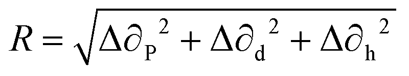
A binary solvent system is mainly composed of a main solvent as well as an additive solvent. When the additive solvent is mixed with the main solvent, the molecular structure of the additive solvent can have a significant impact on tuning the evaporation rate of the binary solvent system as well as on modifying the dissolving of the solute. In a solution that is composed of both solute and solvent, three different types of intermolecular interactions can exist, between solute and solute, between solvent and solvent, as well as between solute and solvent. The solvent's affinity for solute material can determine the extent of these intermolecular interactions and regulate other semiconductor crystallization and film formation processes. The Hansen's solubility theory can be employed to estimate the affinity of the solvent for the solute.Three different Hansen's solubility parameters, including ∂p, ∂d, and ∂h, represent the polar, dispersive and hydrogen bonding component of the intermolecular interaction force.160,161 The similarity of these three Hansen's solubility parameters can give rise to good solubility of the solute in the solvent. The mismatch parameter R can be quantitatively obtained based on the following equation:
 | (7) |
Eqn (7) can be utilized to calculate the mismatch parameter and provides a useful baseline for quantitatively assessing the solubility of a solute in a given solvent, and essentially denotes that a larger mismatch parameter leads to lower solubility in the given solvent. The criteria of choosing appropriate binary solvents include the dielectric constant, boiling point as well as the Hansen's solubility parameters. The higher dielectric constant of a solvent means a higher polarity and thereby greater ability for the solvent to stabilize the charges. Similar boiling points of the binary solvents can ensure simultaneous solvent evaporation and greater control of the semiconductor evaporation. In terms of the Hansen's solubility parameters, both solvents in the binary solvent system will have similar solubility parameters. As similar solubility parameters result in a small mismatch parameter based on eqn (7), a preferred choice of solvent shall thereby possess a small value of mismatch parameter.
In the following section, we will mainly review the application of binary solvents in controlling the single crystal growth and the crystal alignment and of organic semiconductors. We will focus our discussion on the effect of binary solvents on improving the semiconductor crystallization, thin film morphology and charge carrier mobilities of thin film transistors. It is important to note that in addition to thin film transistor applications, the binary solvent method has also been reported in the application of gas sensors and optoelectronic devices. For instance, Ogbeide et al. reported a binary solvent of isopropanol (IPA) and 2-butanol as the ink solvent carrier in order to suppress the adverse coffee-ring effect, which improves the printing uniformity and enhances the detection limit of the gas sensor.162 Fo et al. reported binary solvents composed of 1-chloronaphthalene (CN) and diphenyl ether (DPE) as additives to improve the crystallinity and phase segregation domain of the acceptor material, which in turn inhibits charge recombination and enhances power conversion efficiency.163 In addition to the organic semiconductors, the binary solvent system has also been studied on other types of semiconductors such as small molecular MoS2, and C60. For example, Majd et al. reported a binary solvent method composed of N,N-dimethylformamide (DMF) and IPA to obtain two-dimensional MoS2 nanosheets with an enlarged surface area for application in detecting miRNA-155 in breast cancer.164 Wang et al. reported a binary solvent of chitosan and tetrahydrofuran to homogeneously disperse MoS2 nanosheets with ultrathin thickness to tune the smoke safety property of the epoxy (EP) nanocomposites matrix.165 Ghasemi et al. reported a binary solvent method composed of DMF and N-methyl-2-pyrrolidone (NMP) to modulate the size and thickness of MoS2 nanoflakes.166 The resultant MoS2 nanoflakes with few-layer thickness without lateral dimensional shrinking were applied in phototransistor applications and exhibited a decent response to laser excitation. Zhao et al. reported a binary solvent (m-xylene as the main solvent, and IPA, EtOH and MeOH as the secondary/antisolvent solvent) based vapor diffusion method to grow millimeter-length C60 single crystals and to improve photodetector responsivity by 10 times.167
3.1. Application in single crystal growth
Kim et al. reported a solvent exchange method in order to grow TIPS pentacene microribbon single crystals.168 The triisopropylsilyl side groups of TIPS pentacene provide conformational flexibility, giving rise to good solubility in various hydrophobic solvents such as toluene, while enhanced density of the bulky groups allows tight packing of the backbones and maximizes the π–π interactions. Consequently, the TIPS pentacene organic semiconductor is insoluble in solvents with more polarity such as acetonitrile. Thereby, TIPS pentacene was first dissolved in toluene, before the solution was injected into a large volume of acetonitrile. The minimized interactions with the acetonitrile solvent promoted the intermolecular π–π interactions of TIPS pentacene, and gave rise to the formation of long-extended, single crystal microribbons after the solution was deposited via a simple drop casting method for crystallization, as shown by the scanning electron microscopy (SEM) and transmission electron microscopy (TEM) images of Fig. 1(A) and (B), respectively. Fig. 1(C) shows the selected area electron diffraction pattern of a TIPS pentacene microribbon, which demonstrated high crystallinity of the microribbon. Thin film transistors were fabricated based on the microribbon crystal (Fig. 1(D)), producing an enhanced hole mobility of 1.42 cm2 V−1 s−1. This work shows that the single crystalline TIPS pentacene 1D microribbons exhibit a preferred growth direction along the [010] direction which is also parallel with the π–π stacking direction of TIPS pentacene small molecules, resulting in an improved charge carrier mobility. | ||
| Fig. 1 (A) SEM image and (B) TEM image of a TIPS pentacene microribbon crystal grown by using the solvent exchange method. (C) Selected area electron diffraction pattern of a TIPS pentacene microribbon. (D) Polarized optical image of a transistor device based on a TIPS pentacene microribbon as the active layer. Reproduced from ref. 168, with permission from Wiley. | ||
He et al. combined a binary solvent exchange method with a nucleation agent to control and disperse the self-assembly process of TIPS pentacene microribbon single crystals.169 TIPS pentacene, when drop casted from a single solvent toluene, formed misoriented bulk crystals as shown by the polarized optical microscopic images in Fig. 2(a). A solvent-exchange method composed of both toluene and acetonitrile was employed to alter the crystal growth from bulk crystals to microribbon crystals. However, the resultant microribbon crystals were aggregated (Fig. 2(b)). Thereby, the nucleation agent 4-hexylbenzoic acid (HBA) was employed to disperse the aggregated microribbons. HBA was first dissolved in toluene, and was then mixed with acetonitrile at a volume ratio of 1![[thin space (1/6-em)]](https://www.rsc.org/images/entities/char_2009.gif) :50. Subsequently, the TIPS pentacene solution was injected into the HBA/toluene/acetonitrile mixture. After deposition via drop casting, HBA self-assembled onto the substrate forming an interfacial layer, while its hydrophobic tails underwent interactions with the alkyl chains of TIPS pentacene molecules. Consequently, effective dispersion of TIPS pentacene microribbons with more uniform coverage and morphology were observed in the optical images of Fig. 2(c) and (d). Thin film transistors incorporating the dispersed microribbons as the active layer demonstrated a hole mobility of 0.36 cm2 V−1 s−1 as well as a 9 times increase in average mobility when compared to the counterpart based on the pristine crystals. This work showcases that the self-assembled process from the HBA nucleation agent can effectively modulate the nucleation and crystallization of the organic single crystals while simultaneously improving the film uniformity by dispersing single crystal aggregations.
:50. Subsequently, the TIPS pentacene solution was injected into the HBA/toluene/acetonitrile mixture. After deposition via drop casting, HBA self-assembled onto the substrate forming an interfacial layer, while its hydrophobic tails underwent interactions with the alkyl chains of TIPS pentacene molecules. Consequently, effective dispersion of TIPS pentacene microribbons with more uniform coverage and morphology were observed in the optical images of Fig. 2(c) and (d). Thin film transistors incorporating the dispersed microribbons as the active layer demonstrated a hole mobility of 0.36 cm2 V−1 s−1 as well as a 9 times increase in average mobility when compared to the counterpart based on the pristine crystals. This work showcases that the self-assembled process from the HBA nucleation agent can effectively modulate the nucleation and crystallization of the organic single crystals while simultaneously improving the film uniformity by dispersing single crystal aggregations.
 | ||
| Fig. 2 Polarized optical images of (a) pristine TIPS pentacene bulk crystals, (b) TIPS pentacene microribbon crystals, and (c and d) TIPS pentacene microribbon crystals incorporating the HBA small molecule as a nucleation agent. Images (a–c) have the same scale bar. Reproduced from ref. 169, with permission from The Japan Society of Applied Physics. | ||
Li et al. reported a binary solvent based approach to fabricate large TIPS pentacene single crystals with sizes extending to millimeters.170 Two different binary solvent systems, including IPA/toluene and EtOH/toluene, exhibit a positive azeotropic point but opposing polarities. The TIPS pentacene solutions were drop casted in an ambient clean room environment or in a nitrogen environment. Different ratios of the binary solvents were tested, which gave rise to the distinct thin film morphology of the resultant TIPS pentacene crystals as shown in the polarized optical images of Fig. 3. The TIPS pentacene morphology abruptly transitioned to single crystals with a large domain size from polycrystalline films, as the solvent composition of the binary solvents reached the azeotropic point. In particular, the azeotropic point is at 50.1/49.9 for the IPA/toluene solvents and at 59.8/40.2 for the EtOH/toluene solvents. Accordingly, the charge carrier mobility of self-assembly TIPS pentacene large single crystals were enhanced by 4 times to 0.73 cm2 V−1 s−1. Besides, the single crystal-based transistor devices showed a threshold voltage close to zero, implying a high-quality interface between the active layer and the gate dielectric layer. The improved interface quality was attributed to the high crystallinity, well-defined facets of the single crystals, the specific thermodynamics of the azeotrope mixture, as well as the mechanical flexibility of crystal ribbons. This work shows azeotropic binary solvent mixtures provide an effective method to fabricate organic single crystals via a self-assembled process, with crystals ranging from small needles to large parallelepipeds dependent on the binary solvent ratios with respect to the azeotropic point.
 | ||
| Fig. 3 Cross-polarized optical images showing the TIPS pentacene morphology abruptly changed from polycrystalline films to single crystals with a large domain size as the binary solvent ratios reached the azeotropic point: at 50.1/49.9 for the IPA/toluene solvents as shown in (A), and at 59.8/40.2 for the EtOH/toluene solvents as shown in (B). All images share the same scale bar of 200 mm. Reproduced from ref. 170, with permission from Wiley. | ||
Minemawari et al. reported a binary solvent system, including chlorobenzene as the main solvent and DMF as the antisolvent, to deposit single-domain TIPS pentacene film by using a double-shot ink-jet printing (DS-IJP) technique.122 A piezoelectric IJP apparatus mounted with dual IJP heads was employed for the alternate deposition of semiconductor solution microdroplets. Various printing conditions were tested including droplet volume, travel velocity, repetition frequency and deposition sequence of the antisolvent ink and solution ink. Without adding the antisolvent, inkjet printing TIPS pentacene resulted in a nonuniform film with undesirable coffee rings. Thereby, a different deposition sequence involving the main solvent and antisolvent was tested on the morphology of the resultant thin film morphology. For the first sequence, TIPS pentacene/antisolvent ink was deposited first followed by overprinting of the TIPS pentacene/chlorobenzene ink. Optical microscopic images showed plate-like crystals with a large thickness. For the second sequence, TIPS pentacene/chlorobenzene ink was deposited before the TIPS pentacene/antisolvent ink instead. This gave rise to large single crystal domains of TIPS pentacene, yielding a hole mobility of 0.042 cm2 V−1 s−1. The improved hole mobility was due to uniform thin films free of pinholes, enlarged crystal domains as well as uniform film thickness. This work indicates that the crystalline preference of a small molecular organic semiconductor should be a key consideration when optimizing the inkjet printing processes.
Balakrishnan et al. reported the growth of one-dimensional propoxyethyl-PTCDI single crystalline nanobelts using a solvent exchange method.171 The propoxyethyl side chain of propoxyethyl-PTCDI has conformational flexibility and provides sufficient solubility in various hydrophobic solvents such as chloroform. On the other hand, the perylene backbones exhibit tight packing as a result of the small side chain size and increased density. These properties resulted in insolubility of propoxyethyl-PTCDI in more polar solvents. Therefore, when the propoxyethyl-PTCDI/chloroform solvent was injected into a polar solvent such as methanol, it promoted the nanocrystal phase to self-assemble and to form nanobelts. The solution was drop casted onto the substrate for various characterizations. As shown in the SEM image of Fig. 4(A), the propoxyethyl-PTCDI nanobelts were in well-defined nanostructures. The TEM images presented in Fig. 4(B) and (C) showed uniform nanobelt structures. The diffraction pattern indicated sharp diffraction spots, as shown in the inset of Fig. 4(C). The AFM image of propoxyethyl-PTCDI nanobelts was presented in Fig. 4(D), showing an average thickness of 100 nm. This work showcases that a simple self-assembling process in a binary solvent system results in the formation of the uniaxial crystal structure of the nanobelt.
 | ||
| Fig. 4 (A) SEM photo of propoxyethyl-PTCDI nanobelts grown based on the solvent exchange method. (B) TEM image of propoxyethyl-PTCDI nanobelts, with the zoom-in TEM image shown in (C). (D) AFM image of propoxyethyl-PTCDI nanobelts with an average thickness of 100 nm. Reproduced from ref. 171, with permission from the American Chemical Society. | ||
Chae et al. reported DPE and CN as additives to the main solvent in order to tune the crystallization and thin film morphology of TIPS pentacene single crystalline domains.172 TIPS pentacene was first dissolved in the anisole solvent and the solvent additives were mixed at different concentrations including 0.25%, 0.5% and 1% for DPE as well as 0.2%, 0.25% and 0.5% for CN. The TIPS pentacene solution was drop casted onto substrates preheated at various temperatures for crystallization. Polarized optical images indicated 0.5% DPE solvent gave rise to the formation of V-shaped microcrystals with an enlarged crystal width. In addition, 0.2% CN solvent additive caused the TIPS pentacene crystals to form highly packed crystal domains with improved uniformity in the grain size distribution. Accordingly, the highest mobility of 0.73 cm2 V−1 s−1 and 0.71 cm2 V−1 s−1 was obtained from the TIPS pentacene thin film transistors based on the 0.5% DPE and 0.2% CN solvent additive, respectively. The enhanced charge transport was mainly a result of the enlarged grain width and reduced grain boundaries. This work demonstrates a facile solvent additive approach to improve the charge carrier mobility by tuning the grain boundary density and crystalline defects.
The various binary solvent papers reviewed in this section, along with the author, semiconductor material, binary solvent choice, crystallization method, result and mobility, are summarized in Table 1. Although the mobility values reported in section 1 are slightly higher than those based on solvent exchange in section 3, it is important to point out that the higher mobilities can be partially attributed to the following factors. Organic semiconductors reported in more recent years, such as C8-BTBT, tend to have higher mobilities, reaching approximately 50 cm2 V−1 s−1. Also, external alignment methods such as solution shearing, blade coating and bar coating have been reported to enhance the mobility values. Besides, blending organic semiconductors with polymer additives such as polystyrene has been shown to improve the charge transport properties.173 Therefore, the various advantages of the solvent exchange method as reported in this review article shed light on more universal application on other types of high mobility organic semiconductors as well as on combination with these external alignment and polymer blending methods. In general, controlling the binary solvent choices and compositions provide an effective method to modulate the important morphological factors such as crystal orientation, phase segregation, and grain size. Binary solvents composed of a “good” solvent and a “bad” solvent effectively modulate the semiconductor solubility, nucleation, crystallization and crystal alignment. Besides, solvents with a high boiling point possess a slow evaporation rate and provide sufficient time for solute diffusion, which not only promotes more pronounced phase segregation, but also results in an enlarged grain size with reduced grain boundaries and crystalline defects.
| Author | Semiconductor | Binary solvent | Crystallization method | Result | Mobility (cm2 V−1 s−1) |
|---|---|---|---|---|---|
| Kim et al. | TIPS pentacene | Toluene/acetonitrile | Drop casting | Solvent exchange method promoted the intermolecular π–π interactions and formed single crystalline microribbons | 1.42 |
| He et al. | TIPS pentacene | Toluene/acetonitrile | Drop casting | Solvent exchange method, combined with a nucleation agent, was used to disperse the aggregated microribbons | 0.36 |
| Li et al. | TIPS pentacene | IPA/toluene, EtOH/toluene | Drop casting | Binary solvents with a positive azeotropic point but opposing polarities gave rise to large single crystals | 0.73 |
| Minemawari et al. | TIPS pentacene | Chlorobenzene/DMF | Ink-jet printing | Adding DMF as an antisolvent ink eliminated the coffee ring and led to large single crystal domains | 0.042 |
| Balakrishnan et al. | Propoxyethyl-PTCDI | Chloroform/methanol | Drop casting | Binary solvent promoted the nanocrystal phase to self-assemble and form well-defined nanostructures | Not reported |
| Chae et al. | TIPS pentacene | Anisole/DPE or CN | Drop casting | Binary solvent with solvent additive led to V-shaped microcrystals and highly packed enlarged crystal domains | 0.73 |
3.2. Application in crystal alignment
He et al. combined the binary solvent method with a controlled solvent evaporation method to realize the aligned crystallization of a p-type organic semiconductor 5,6,11,12-tetrachlorotetracene.50 The binary solvent system is composed of a chloroform solvent as the “good” solvent and a methanol solvent as the “bad” solvent. The organic semiconductor 5,6,11,12-tetrachlorotetracene was first dissolved in the chloroform solvent and the solution was then injected into methanol, which caused supramolecular aggregations to form as indicated by the blue shift in the UV-vis absorption spectra. These supramolecular aggregations serve as seeds for the 5,6,11,12-tetrachlorotetracene semiconductor to nucleate and crystallize. In the meantime, a controlled solvent evaporation method was applied to induce capillary force, which aligned the growth direction of the 5,6,11,12-tetrachlorotetracene semiconductor. In order to optimize the thin film morphology and crystal alignment, different ratios between chloroform and methanol including 1:0, 10:1, 5:1, and 3:1 were tested. A simple drop casting method was adopted to deposit the organic semiconductor solution. As shown in the polarized optical images of Fig. 5, without the methanol solvent, the 5,6,11,12-tetrachlorotetracene crystal growth based on the pure chloroform solvent showed random patterns, leaving a majority of the substrate uncovered with crystals. In contrast, both crystal alignment and substrate coverage were enhanced at 10:1 and 5:1 ratios of the chloroform/methanol binary solvent. When the ratio further changed to 3:1, the alignment started to wane. Electrical characterization results indicated that the 5,6,11,12-tetrachlorotetracene based thin film transistors with chloroform/methanol binary solvent at 10:1 exhibited an improved hole mobility of 1.1 cm2 V−1 s−1, which was attributed to the improved crystal alignment and coverage. This work shows the solvent exchange method effectively modulates the supramolecular aggregations, nucleation formation and crystallization of the organic semiconductor 5,6,11,12-tetrachlorotetracene, and when in combination with the controlled solvent evaporation method, can powerfully lead to the directional alignment of crystal growth.
 | ||
| Fig. 5 Polarized optical images showing the thin film morphologies of 5,6,11,12-tetrachlorotetracene crystals grown by drop casting in binary solvents and applying the controlled solvent evaporation method. The images in (a–d) correspond to chloroform/methanol binary solvent at ratios of 1:0, 10:1, 5:1, and 3:1, respectively. The images in (a–d) have the same scale bar of 100 microns. Reproduced from ref. 50, with permission from Elsevier. | ||
A similar method of combining controlled evaporation with a binary solvent system was also employed to realize the organized crystallization of SMDPPEH.51 In this work, Bi et al. used chloroform as the good solvent and ethanol as the bad solvent. The controlled evaporative self-assembly method, abbreviated as “CESA”, involved the placement of a Pinner on the substrate to induce capillary force. The SMDPPEH solution was deposited onto the substrate with a preset Pinner via a simple drop casting method. The resultant thin film morphology of SMDPPEH, in terms of crystal orientation alignment, film coverage as well as grain width, was observed to correlate to the different ratios between chloroform and ethanol. The misorientation angle was calculated to more accurately evaluate the change of crystal alignment with different binary solvent ratios. At ratios of 15:1, 10:1, 5:1, 1:1 and 1:5, average misorientation angles of 6 ± 5°, 4 ± 3°, 4 ± 2°, 11 ± 7° and 30 ± 20° were measured, respectively, which indicated the greatest advances in alignment at both 10:1 and 5:1 ratios. The aligned SMDPPEH crystal based OTFTs at the binary solvent ratio of 5:1 exhibited an enhanced mobility of 0.016 cm2 V−1 s−1. The binary solvent method in combination with the CESA method as reported in this work effectively controls the contact line pinning, enhances the evaporation rate at the droplet edge, elevates the solution concentration, facilitates outward flow of solute, promotes nucleation formation, and improves crystallization.
Abdullah et al. reported the impact of anisole/decane binary solvents on the crystallization and thin film morphology of TIPS pentacene.113 When the composition of the anisole/decane binary solvent ranged between 96/4 wt% and 85/15 wt%, an azeotropic composition is maintained in the solution mixture, giving rise to a constant boiling point at 152 °C as well as constant binary solvent composition during the solvent evaporation. TIPS pentacene solution was drop casted at a temperature of 30 °C onto a slightly tilted substrate and allowed to dry for 3 hours. As the content of decane increased, the interaction between the solute and solvent became weakened, which promoted the nucleation of TIPS pentacene and consequently the formation of large crystals. The TIPS pentacene film deposited from pure anisole solvent showed grain like nanodots with a roughness of 6.3 nm. When the anisole was mixed with decane at 96/4 wt% and 90/10 wt%, the TIPS pentacene film changed to a terrace like morphology with a larger surface roughness. To fabricate the thin film transistors, a polyvinyl pyrrolidone (PVP) and poly(melamine-co-formaldehyde) hybrid layer was used as the gate dielectric before TIPS pentacene was drop casted in the binary solvents to form the active layer. A hole mobility of up to 0.16 cm2 V−1 s−1 was obtained based on the 93/7 wt% binary solvent. This work shows that the binary solvents composed of anisole and decane can effectively modulate the mean size of nanodots of TIPS pentacene as well as its average surface roughness, promoting step-flow crystal growth, layer ordering and long-range alignment.
Bharti et al. studied the correlation between the dissimilarity of binary solvents, the molecular aggregation, and the charge transport of organic semiconductors.123 In this work, TIPS pentacene was dissolved in different solvents including single solvent toluene, as well as binary solvents of toluene/benzene, toluene/cyclohexane, and toluene/hexane. A simple drop casting method was used to dispense the TIPS pentacene solution on a tilted substrate. The addition of hexane as a nonsolvent effectively resulted in a weaker repulsive force between the TIPS pentacene solute molecules and thereby stronger molecular aggregations due to enhanced molecular interactions. Terracing structures of TIPS pentacene were obtained based on the single solvent. The addition of cyclohexane and hexane, which exhibit more different structures from that of toluene, resulted in more irregular terracing structures of TIPS pentacene. In particular, hexane has the most dissimilar structure with toluene and hence promotes the strongest molecular aggregation of TIPS pentacene. As a result, TIPS pentacene crystals grown based on the toluene/hexane binary solvent showed improved crystallinity and the highest hole mobility of 0.15 cm2 V−1 s−1. This work demonstrates that increased dissimilarity of the additive solvent in the binary solvent system makes it more challenging to overcome intermolecular forces and thereby favors molecular aggregation of TIPS pentacene, leading to enhanced crystallinity.
Lim et al. reported the effect of solvent mixture including chlorobenzene as the main solvent and hexane, o-dichlorobenzene or dodecane as the additive solvent to tune the crystal growth and alignment of TIPS pentacene.118 An ink-jet printer mounted with a single-nozzle piezoelectric head and a two-axis motorized positioning system was employed to deposit 40–50 picoliters of the TIPS pentacene solution onto the substrate which is 0.5 mm away from the head. TIPS pentacene deposited from chlorobenzene resulted in a homogeneous film but undesirable molecular misorientations, as shown in the optical image of Fig. 6(a). Thereby, various solvents including hexane, o-dichlorobenzene or dodecane, were mixed with chlorobenzene as a solvent additive. The resultant thin film morphology was presented in Fig. 6(b)–(d), respectively. The addition of hexane resulted in thicker aggregation of TIPS pentacene at the perimeter of the inkjet printed droplets. Mixing o-dichlorobenzene with the main solvent led to a more uniform morphology (Fig. 6(b)). Besides, hexane, which has a high boiling point, allows a recirculation flow of the solution and also induces a Marangoni flow that contradicts the convective flow (Fig. 6(c)). TIPS pentacene crystals deposited from the chlorobenzene/dodecane binary solvent showed orientation enhancement, as shown in the optical image of Fig. 6(d). As a result, the best average hole mobility of 0.12 cm2 V−1 s−1 was obtained from the inkjet printed TIPS pentacene based on the chlorobenzene/dodecane binary solvent. This work reveals that in order to obtain highly aligned TIPS pentacene crystals with high crystallinity, it is important to ensure the minor solvent has a higher boiling point as well as lower surface tension than the main solvent, which induces a recirculation flow opposite to the convective flow and promotes crystal self alignment.
 | ||
| Fig. 6 Optical microscopic images of inkjet printed TIPS pentacene films based on different solvent choices including (a) chlorobenzene, (b) chlorobenzene/hexane, (c) chlorobenzene/o-dichlorobenzene, and (d) chlorobenzene/dodecane. The volume ratio of chlorobenzene is maintained at 25% for all cases. Reproduced from ref. 118, with permission from Wiley. | ||
Zhao et al. reported a binary solvent method to grow large scaled TIPS pentacene crystals with orientation alignment.174 A Marangoni effect-controlled oriented growth (MOG) method was used to enable large-area deposition of TIPS pentacene solution and allowed the substrate to move in an upward and downward manner, which promoted contact line pinning, liquid membrane spreading, film formation and crystal alignment. The binary solvent system is composed of toluene and carbon tetrachloride with different boiling points. Carbon tetrachloride has a low boiling point and high surface tension, whereas toluene has a high boiling point and low surface tension. Since the solvent evaporation had a faster rate at the contact line than inside the liquid interior, the composition of toluene in the binary solvent at the contact time increased over time due to its higher boiling point. As a result, the contact line had a lower surface tension, which created a Marangoni flow from the contact line towards the liquid interior. This Marangoni flow further counterbalanced the convective flow and promoted a recirculation flow, giving rise to well-aligned TIPS pentacene crystals with large scaled domain size. As a result, the TIPS pentacene thin film transistors based on the binary solvent showed a mobility of 0.7 ± 0.22 cm2 V−1 s−1. The MOG method in combination with the binary solvent method is effective in promoting directed formation of semiconducting small molecules and self-organization of highly aligned crystalline structures.
Lada et al. reported a binary solvent system in order to tune the morphology and charge transport of TIPS pentacene.175 The solvent system is composed of mesitylene as the main solvent, and a series of additive solvents including two types of alkyl aromatics (cumene and indane), two types of aromatic acetates (butyl and amyl acetate) and two types of aromatic ethers (anisole and 4-methylanisole), which give rise to a range of boiling points close to that of the main solvent. TIPS pentacene and the polymer additive PS finds good solubility in the main solvent and additive solvent, respectively. The TIPS pentacene solution with PS additive was deposited via spin coating. Optical images showed that TIPS pentacene film exhibited small crystallite size when deposited in the single solvent, generating a low mobility of 0.1 cm2 V−1 s−1. In contrast, adding anisole as the additive solvent yielded a considerable increase in the crystal size of TIPS pentacene, and thereby generated a much higher saturation mobility of 1.16 cm2 V−1 s−1 as well as a lower threshold voltage due to the reduced number of grain boundaries. This work demonstrates choosing the appropriate solubility differentials of the binary solvents promoting phase segregation, crystallite size as well as active layer flatness.
The various binary solvent papers reviewed In this section, along with the author, semiconductor material, binary solvent choice, crystallization method, result and mobility, are summarized in Table 2.
| Author | Semiconductor | Binary solvent | Crystallization method | Result | Mobility (cm2 V−1 s−1) |
|---|---|---|---|---|---|
| He et al. | 5,6,11,12-Tetrachlorotetracene | Chloroform/methanol | Drop casting | Binary solvents promoted supramolecular aggregations to form as nucleation seeds | 1.1 |
| Bi et al. | SMDPPEH | Chloroform/ethanol | Drop casting | Binary solvents along with a “CESA” method reduced crystal misorientation and improved alignment | 0.016 |
| Abdullah et al. | TIPS pentacene | Anisole/decane | Drop casting | Binary solvents promoted semiconductor nucleation and formation of large crystals | 0.16 |
| Bharti et al. | TIPS pentacene | Toluene/benzene, cyclohexane, or hexane | Drop casting | Solvent additive with the most dissimilar structure promoted the strongest molecular aggregation and improved crystallinity | 0.15 |
| Lim et al. | TIPS pentacene | Chlorobenzene/hexane, o-dichlorobenzene or dodecane | Ink-jet printing | Binary solvent with dodecane additive led to enhanced orientation alignment | 0.12 |
| Zhao et al. | TIPS pentacene | Toluene/carbon tetrachloride | MOG method | Binary solvent created Marangoni flow that counterbalanced convective flow and promoted crystal alignment | 0.7 ± 0.22 |
| Lada et al. | TIPS pentacene | Mesitylene/various aromatics-based solvents | Spin coating | Binary solvent incorporating hexane increased the crystal size of TIPS pentacene and reduced grain boundaries | 1.16 |
4. Summary and outlook
In this work, we have reviewed a binary solvent technique for modulating the organic semiconductor nucleation, controlling the crystallization behavior, improving the film crystallinity and enhancing the charge transport of organic semiconductor based thin film transistors. Using TIPS pentacene as a primary example for the general solution processed, organic semiconductors, we discussed the effects of engineering different solvent choices on the organic semiconductor thin film morphologies, phase segregation, grain width and crystal orientation. We also explored the important correlation between the different solvent choice, thin film morphology and charge carrier mobility of the organic semiconductor based thin film transistors. These works demonstrated that binary solvents can provide an effective approach to promote supramolecular aggregation, counterbalance undesirable convective flow, and enhance crystal orientation alignment when combined with miscellaneous external alignment methods.Organic semiconductor based thin film transistors can be implemented in a variety of device applications such as photodetectors, gas sensors and logic circuits. The exploration and optimization of the solvent choices for solution processed organic semiconductors becomes more important when future endeavors are made to expand the application of organic semiconductors in these related electrical device fabrications. Future research in the following aspects will shed light on the pathway to achieve high performance flexible electronics. First of all, binary solvent is an effective method to induce the crystallization of single crystals. A single crystal is free of grain boundaries and crystalline defects, which can yield ultra-high charge carrier mobilities and thereby have significant applications for high performance flexible electronic devices.176–180 Besides, ternary solvents, as opposed to a single solvent or binary solvent, have been extensively demonstrated to control the domain of size of perovskite films for enhancing solar cell performances.181,182 The ternary solvent system could be a potential pathway to control the crystallization of solution processed organic semiconductors since it has been reported to effectively improve the semiconductor morphology uniformity, enhance the crystal alignment in a long range order, control the domain size, and modulate the interface. These factors exert positive effects on organic semiconductor charge transport: improved crystal morphology uniformity and long-range alignment improves crystal bridging of contact electrodes and ensures efficient charge transport; enlarged domain sizes help diminish grain boundaries, crystalline defects and charge trap centers; improved quality of the interface between the semiconductor active layer and dielectric layer gives rise to better charge transport. Furthermore, due to the increasingly urgent call for a green environment, green solvents such as n-amyl acetate or 1,3-dioxolane provide an effective alternative to the binary solvent while simultaneously bringing little to no toxicity to the environment.183,184 Finally, miscellaneous external alignment methods such as bar-casting,185–188 dip-casting,189–194 drop-pinned crystallization,195–198 off-center coating199–205 have been previously reported as highly effective in aligning the crystal orientation, patterning crystals on a large area, improving areal coverage and continuity, which is preferred to enhance charge transport capability. While previous binary solvent studies mainly employ drop casting as the crystallization method as shown in this review article, combining these methods with the binary solvent method, thereby, would further improve the charge carrier properties and expand the application in organic optoelectronics or organic circuits. We expect that future efforts in these aforementioned aspects will expedite the progress of flexible electronic devices.
Conflicts of interest
There are no conflicts to declare.Acknowledgements
S. Bi acknowledges the support from the Science and Technology Project of Liaoning Province (20180540006).References
- M. R. Cavallari, L. M. Pastrana, C. D. Sosa, A. M. Marquina, J. E. Izquierdo, F. J. Fonseca, C. A. Amorim, L. G. Paterno and I. Kymissis, Organic Thin-Film Transistors as Gas Sensors: A Review, Materials, 2021, 14, 3 CrossRef CAS PubMed.
- A. K. Gupta, Z. Zhang, E. Spuling, M. Kaczmarek, Y. Wang, Z. Hassan, I. D. W. Samuel, S. Braese and E. Zysman-Colman, Electron-withdrawing Group Modified Carbazolophane Donors for Deep Blue Thermally Activated Delayed Fluorescence OLEDs, Mater. Adv., 2021, 6684–6693 RSC.
- R. Colucci, H. F. d P. Barbosa, F. Günther, P. Cavassin and G. C. Faria, Recent advances in modeling organic electrochemical transistors, Flexible Printed Electron., 2020, 5, 013001 CrossRef CAS.
- W. Zhou, N. J. Yutronkie, B. H. Lessard and J. L. Brusso, From chemical curiosity to versatile building blocks: unmasking the hidden potential of main-group phthalocyanines in organic field-effect transistors, Mater. Adv., 2021, 2, 165–185 RSC.
- S. Bi, W. Jin, X. Han, X. Cao, Z. He, K. Asare-Yeboah and C. Jiang, Ultra-Fast-Responsivity with Sharp Contrast Integrated Flexible Piezo Electrochromic Based Tactile Sensing Display, Nano Energy, 2022, 107629 CrossRef CAS.
- M. J. Mirshojaeian Hosseini and R. A. Nawrocki, A Review of the Progress of Thin-Film Transistors and Their Technologies for Flexible Electronics, Micromachines, 2021, 12, 655 CrossRef PubMed.
- K. J. Thorley, M. Benford, Y. Song, S. R. Parkin, C. Risko and J. E. Anthony, What is special about silicon in functionalised organic semiconductors?, Mater. Adv., 2021, 2, 5415–5421 RSC.
- A. Salehi, X. Fu, D.-H. Shin and F. So, Recent Advances in OLED Optical Design, Adv. Funct. Mater., 2019, 29, 1808803 CrossRef.
- Z. Lin, X. Guo, L. Zhou, C. Zhang, J. Chang, J. Wu and J. Zhang, Solution-processed high performance organic thin film transistors enabled by roll-to-roll slot die coating technique, Org. Electron., 2018, 54, 80–88 CrossRef CAS.
- C. T. da Rocha, K. Haase, Y. C. Zheng, M. Loffler, M. Hambsch and S. C. B. Mannsfeld, Solution Coating of Small Molecule/Polymer Blends Enabling Ultralow Voltage and High-Mobility Organic Transistors, Adv. Electron. Mater., 2018, 4, 1800141 CrossRef.
- Z. He, Z. Zhang and S. Bi, Nanoparticles for organic electronics applications, Mater. Res. Express, 2020, 7, 012004 CrossRef CAS.
- M. Uno, T. Uemura, Y. Kanaoka, Z. H. Chen, A. Facchetti and J. Takeya, High-speed organic single-crystal transistors gated with short-channel air gaps: Efficient hole and electron injection in organic semiconductor crystals, Org. Electron., 2013, 14, 1656–1662 CrossRef CAS.
- T. Zimmerling and B. Batlogg, Improving charge injection in high-mobility rubrene crystals: From contact-limited to channel-dominated transistors, J. Appl. Phys., 2014, 115, 164511 CrossRef.
- H. Chang, W. Li, H. Tian, Y. Geng, H. Wang, D. Yan and T. Wang, High performance of rubrene thin film transistor by weak epitaxy growth method, Org. Electron., 2015, 20, 43–48 CrossRef CAS.
- Z. Wang, H. Guo, J. Li, L. Wang and G. Dong, Marangoni Effect-Controlled Growth of Oriented Film for High Performance C8-BTBT Transistors, Adv. Mater. Interfaces, 2019, 6, 1801736 CrossRef.
- J. Panidi, A. F. Paterson, D. Khim, Z. P. Fei, Y. Han, L. Tsetseris, G. Vourlias, P. A. Patsalas, M. Heeney and T. D. Anthopoulos, Remarkable Enhancement of the Hole Mobility in Several Organic Small-Molecules, Polymers, and Small-Molecule:Polymer Blend Transistors by Simple Admixing of the Lewis Acid p-Dopant B(C6F5)(3), Adv. Sci., 2018, 5, 1700290 CrossRef PubMed.
- J.-m Cho, T. Higashino and T. Mori, Band-like transport down to 20K in organic single-crystal transistors based on dioctylbenzothienobenzothiophene, Appl. Phys. Lett., 2015, 106, 193303 CrossRef.
- S. Tazuhara, T. Nagase, T. Kobayashi, Y. Sadamitsu and H. Naito, Understanding the influence of contact resistances on short-channel high-mobility organic transistors in linear and saturation regimes, Appl. Phys. Express, 2021, 14, 041010 CrossRef CAS.
- Z. Chen, S. Duan, X. Zhang, B. Geng, Y. Xiao, J. Jie, H. Dong, L. Li and W. Hu, Organic Semiconductor Crystal Engineering for High-Resolution Layer-Controlled 2D Crystal Arrays, Adv. Mater., 2021, 34, 2104166 CrossRef PubMed.
- Y. Zhu, Y. Fan, S. Li, P. Wei, D. Li, B. Liu, D. Cui, Z. Zhang, G. Li, Y. Nie and G. Lu, Soluble poly(4-fluorostyrene): a high-performance dielectric electret for organic transistors and memories, Mater. Horiz., 2020, 7, 1861–1871 RSC.
- Z. Chen, S. Duan, X. Zhang and W. Hu, Dual-function surfactant strategy for two-dimensional organic semiconductor crystals towards high-performance organic field-effect transistors, Sci. China: Chem., 2021, 64, 1057–1062 CrossRef CAS.
- D. K. Hwang, C. Fuentes-Hernandez, J. B. Kim, W. J. Potscavage and B. Kippelen, Flexible and stable solution-processed organic field-effect transistors, Org. Electron., 2011, 12, 1108–1113 CrossRef CAS.
- D. Bharti and S. P. Tiwari, Phase separation induced high mobility and electrical stability in organic field-effect transistors, Synth. Met., 2016, 221, 186–191 CrossRef CAS.
- S. K. Park, D. A. Mourey, J. I. Han, J. E. Anthony and T. N. Jackson, Environmental and operational stability of solution-processed 6,13-bis(triisopropyl-silylethynyl) pentacene thin film transistors, Org. Electron., 2009, 10, 486–490 CrossRef CAS.
- Y. Takumi, F. Hiroki, K. Yoshinari, H. Yoshiaki and K. Masatoshi, Wide-range work function tuning in gold surfaces modified with fluorobenzenethiols toward application to organic thin-film transistors, Flexible Printed Electron., 2020, 5, 014011 CrossRef.
- K. Asare-Yeboah, S. Bi, Z. He and D. Li, Temperature gradient controlled crystal growth from TIPS pentacene-poly(alpha-methyl styrene) blends for improving performance of organic thin film transistors, Org. Electron., 2016, 32, 195–199 CrossRef CAS.
- Z. He, S. Shaik, S. Bi, J. Chen and D. Li, Air-stable solution-processed n-channel organic thin film transistors with polymer-enhanced morphology, Appl. Phys. Lett., 2015, 106, 183301 CrossRef.
- R. Basu, A review on single crystal and thin film Si–Ge alloy: growth and applications, Mater. Adv., 2022, 3, 4489–4513 RSC.
- S. Hou, X. Zhuang, H. Fan and J. Yu, Grain Boundary Control of Organic Semiconductors via Solvent Vapor Annealing for High-Sensitivity NO2 Detection, Sensors, 2021, 21, 226 CrossRef CAS PubMed.
- N. Caicedo, R. Leturcq, J. P. Raskin, D. Flandre and D. Lenoble, Detection mechanism in highly sensitive ZnO nanowires network gas sensors, Sens. Actuators, B, 2019, 297, 126602 CrossRef CAS.
- A. Rianjanu, R. Aflaha, N. I. Khamidy, M. Djamal, K. Triyana and H. S. Wasisto, Room-temperature ppb-level trimethylamine gas sensors functionalized with citric acid-doped polyvinyl acetate nanofibrous mats, Mater. Adv., 2021, 2, 3705–3714 RSC.
- R. Malik, N. Joshi and V. K. Tomer, Advances in the designs and mechanisms of MoO3 nanostructures for gas sensors: a holistic review, Mater. Adv., 2021, 2, 4190–4227 RSC.
- J. M. Suh, T. H. Eom, S. H. Cho, T. Kim and H. W. Jang, Light-activated gas sensing: a perspective of integration with micro-LEDs and plasmonic nanoparticles, Mater. Adv., 2021, 2, 827–844 RSC.
- K. Asare-Yeboah, Q. Li, C. Jiang, Z. He, S. Bi, Y. Liu and C. Liu, High Performance and Efficiency Resonant Photo-Effect-Transistor by Near-Field Nano-Strip-Controlled Organic Light Emitting Diode Gate, J. Phys. Chem. Lett., 2020, 11, 6526–6534 CrossRef CAS PubMed.
- S. Bi, Q. Li, Z. He, Q. Guo, K. Asare-Yeboah, Y. Liu and C. Jiang, Highly enhanced performance of integrated piezo photo-transistor with dual inverted OLED gate and nanowire array channel, Nano Energy, 2019, 66, 104101 CrossRef CAS.
- M. Y. Lee, J. Park and J. H. Oh, High-Performance Ambipolar Organic Phototransistors Based on Core–Shell p–n Junction Organic Single Crystals, ACS Appl. Electron. Mater., 2020, 2, 9–18 CrossRef.
- M. Mamada, H. Nakanotani and C. Adachi, Amplified spontaneous emission from oligo(p-phenylenevinylene) derivatives, Mater. Adv., 2021, 2, 3906–3914 RSC.
- S. Ghosh, H. Shankar and P. Kar, Recent developments of lead-free halide double perovskites: a new superstar in the optoelectronic field, Mater. Adv., 2022, 3, 3742–3765 RSC.
- R. E. Aderne, B. G. A. L. Borges, H. C. Ávila, F. von Kieseritzky, J. Hellberg, M. Koehler, M. Cremona, L. S. Roman, C. M. Araujo, M. L. M. Rocco and C. F. N. Marchiori, On the energy gap determination of organic optoelectronic materials: the case of porphyrin derivatives, Mater. Adv., 2022, 3, 1791–1803 RSC.
- S. Bi, W. Zhao, Y. Sun, C. Jiang, Y. Liu, Z. He, Q. Li and J. Song, Dynamic photonic perovskite light-emitting diodes with post-treatment-enhanced crystallization as writable and wipeable inscribers, Nanoscale Adv., 2021, 3, 6659–6668 RSC.
- Z. Yang, S. Lin, J. Liu, K. Zheng, G. Lu, B. Ye, J. Huang, Y. Zhang, Y. Ye, T. Guo and G. Chen, Integration of highly crystalline C8-BTBT thin-films into simple logic gates and circuits, Org. Electron., 2020, 78, 64–71 Search PubMed.
- H. J. Cho, D.-H. Lee, E.-K. Park, M. S. Kim, S. Y. Lee, K. Park, H. Choe, J.-H. Jeon and Y.-S. Kim, Solution-processed organic-inorganic hybrid gate insulator for complementary thin film transistor logic circuits, Thin Solid Films, 2019, 673, 14–18 CrossRef CAS.
- A. Bilgaiyan, S.-I. Cho, M. Abiko, K. Watanabe and M. Mizukami, Flexible, high mobility short-channel organic thin film transistors and logic circuits based on 4H–21DNTT, Sci. Rep., 2021, 11, 11710 CrossRef CAS PubMed.
- Y. Sun, Z. Zhang, K. Asare-Yeboah, S. Bi and Z. He, Poly(butyl acrylate) polymer enhanced phase segregation and morphology of organic semiconductor for solution-processed thin film transistors, J. Appl. Polym. Sci., 2021, 138, 50654 CrossRef CAS.
- Z. He, K. Asare-Yeboah, Z. Zhang and S. Bi, Manipulate organic crystal morphology and charge transport, Org. Electron., 2022, 103, 106448 CrossRef CAS.
- J. H. Chen, D. C. Martin and J. E. Anthony, Morphology and molecular orientation of thin-film bis(triisopropylsilylethynyl) pentacene, J. Mater. Res., 2007, 22, 1701–1709 CrossRef CAS.
- K. Asare-Yeboah, R. M. Frazier, G. Szulczewski and D. Li, Temperature gradient approach to grow large, preferentially oriented 6,13-bis(triisopropylsilylethynyl) pentacene crystals for organic thin film transistors, J. Vac. Sci. Technol., B: Nanotechnol. Microelectron.: Mater., Process., Meas., Phenom., 2014, 32, 052401 Search PubMed.
- Z. He, Z. Zhang, S. Bi, K. Asare-Yeboah and J. Chen, Ultra-low misorientation angle in small-molecule semiconductor/polyethylene oxide blends for organic thin film transistors, J. Polym. Res., 2020, 27, 75 CrossRef CAS.
- H. B. Akkerman, H. Y. Li and Z. N. Bao, TIPS-pentacene crystalline thin film growth, Org. Electron., 2012, 13, 2056–2062 CrossRef CAS.
- Z. He, N. Lopez, X. Chi and D. Li, Solution-based 5,6,11,12-tetrachlorotetracene crystal growth for high-performance organic thin film transistors, Org. Electron., 2015, 22, 191–196 CrossRef CAS.
- S. Bi, Z. He, J. Chen and D. Li, Solution-grown small-molecule organic semiconductor with enhanced crystal alignment and areal coverage for organic thin film transistors, AIP Adv., 2015, 5, 077170 CrossRef.
- Z. He, K. Xiao, W. Durant, D. K. Hensley, J. E. Anthony, K. Hong, S. M. Kilbey, II, J. Chen and D. Li, Enhanced Performance Consistency in Nanoparticle/TIPS Pentacene-Based Organic Thin Film Transistors, Adv. Funct. Mater., 2011, 21, 3617–3623 CrossRef CAS.
- Z. He, Z. Zhang and S. Bi, Long-range crystal alignment with polymer additive for organic thin film transistors, J. Polym. Res., 2019, 26, 173 CrossRef.
- J. H. Chen, C. K. Tee, M. Shtein, J. Anthony and D. C. Martin, Grain-boundary-limited charge transport in solution-processed 6,13 bis(tri-isopropylsilylethynyl) pentacene thin film transistors, J. Appl. Phys., 2008, 103, 114513 CrossRef.
- Z. He, Z. Zhang, S. Bi, K. Asare-Yeboah, J. Chen and D. Li, A facile and novel route to improve TIPS pentacene based organic thin film transistor performance with elastomer, Synth. Met., 2020, 262, 116337 CrossRef CAS.
- Z. He, J. Chen and D. Li, Polymer Additive Controlled Morphology for High Performance Organic Thin Film Transistors, Soft Matter, 2019, 15, 5790–5803 RSC.
- Z. He, Z. Zhang and S. Bi, Tailoring the molecular weight of polymer additives for organic semiconductors, Mater. Adv., 2022, 3, 1953–1973 RSC.
- L.-H. Chou, W.-C. Chang, G.-Y. He, Y.-C. Chiu and C.-L. Liu, Controllable electrical performance of spray-coated semiconducting small molecule/insulating polymer blend thin film for organic field effect transistors application, React. Funct. Polym., 2016, 108, 130–136 CrossRef CAS.
- J. I. Han, C.-Y. Lim, S. K. Park and Y.-H. Kim, High-Performance 2,8-Difluoro-5,11-bis(triethylsilylethynyl) Anthradithiophene Thin-Film Transistors Facilitated by Predeposited Ink-Jet Blending, Jpn. J. Appl. Phys., 2013, 52, 031601 CrossRef.
- N. L. Vaklev, R. Muller, B. V. O. Muir, D. T. James, R. Pretot, P. van der Schaaf, J. Genoe, J. S. Kim, J. H. G. Steinke and A. J. Campbell, High-Performance Flexible Bottom-Gate Organic Field-Effect Transistors with Gravure Printed Thin Organic Dielectric, Adv. Mater. Interfaces, 2014, 1, 1300123 CrossRef PubMed.
- H. L. Zhong, J. Smith, S. Rossbauer, A. J. P. White, T. D. Anthopoulos and M. Heeney, Air-Stable and High-Mobility n-Channel Organic Transistors Based on Small-Molecule/Polymer Semiconducting Blends, Adv. Mater., 2012, 24, 3205–3211 CrossRef CAS PubMed.
- Z. Zhang, K. Asare-Yeboah, S. Bi and Z. He, Poly(α-methyl styrene) polymer additive for organic thin film transistors, J. Mater. Sci.: Mater. Electron., 2022, 33, 1101–1122 CrossRef CAS.
- N. Onojima, N. Akiyama, Y. Mori, T. Sugai and S. Obata, Small molecule/polymer blends prepared by environmentally-friendly process for mechanically-stable flexible organic field-effect transistors, Org. Electron., 2020, 78, 105597 CrossRef CAS.
- S. Hou, J. Yu, X. Zhuang, D. Li, Y. Liu, Z. Gao, T. Sun, F. Wang and X. Yu, Phase separation of P3HT/PMMA blend film formed semiconducting and dielectric layers in organic thin film transistors for high sensitivity NO2 detection, ACS Appl. Electron. Mater., 2019, 11, 44521–44527 CrossRef CAS PubMed.
- S. Y. Yeo, S. Park, Y. J. Yi, D. H. Kim and J. A. Lim, Highly Sensitive Flexible Pressure Sensors Based on Printed Organic Transistors with Centro-Apically Self-Organized Organic Semiconductor Microstructures, ACS Appl. Mater. Interfaces, 2017, 9, 42996–43003 CrossRef CAS PubMed.
- N. Onojima, K. Hara and A. Nakamura, Vertical phase separation of 6,13-bis(triisopropylsilylethynyl) pentacene/poly(methyl methacrylate) blends prepared by electrostatic spray deposition for organic field-effect transistors, Jpn. J. Appl. Phys., 2017, 56, 5S2 CrossRef.
- L. Zhang, D. Yang, Y. Wang, H. Wang, T. Song, C. Fu, S. Yang, J. Wei, R. Liu and B. Zou, Performance Enhancement of FET-Based Photodetector by Blending P3HT With PMMA, IEEE Photonics Technol. Lett., 2015, 27, 1535–1538 CAS.
- J. Soeda, T. Okamoto, C. Mitsui and J. Takeya, Stable growth of large-area single crystalline thin films from an organic semiconductor/polymer blend solution for high-mobility organic field-effect transistors, Org. Electron., 2016, 39, 127–132 CrossRef CAS.
- Z. Yang, S. Lin, J. Liu, K. Zheng, G. Lu, B. Ye, J. Huang, Y. Zhang, Y. Ye, T. Guo and G. Chen, Sharp phase-separated interface of 6, 13-bis (triisopropylsilylethynyl) pentacene/polystyrene blend films prepared by electrostatic spray deposition, Org. Electron., 2020, 78, 206–210 Search PubMed.
- X. Xiao, G. Pan and F. Zhang, High transparency and enhanced mobility of field-effect transistors of the semiconductor/insulator polymer blends with ultralow semiconductor content, Org. Electron., 2020, 82, 105709 CrossRef CAS.
- N. Onojima, Y. Mori, T. Ozawa, T. Sugai, N. Akiyama and S. Obata, Flexible organic field-effect transistors based on 6,13-bis(triisopropylsilylethynyl) pentacene/polystyrene blend film prepared by electrostatic spray deposition, Jpn. J. Appl. Phys., 2019, 59, SDDA13 CrossRef.
- T. Shen, H. Zhou, J. Xin, Q. Fan, Z. Yang, J. Wang, T. Mei, X. Wang, N. Wang and J. Li, Controllable microstructure of polymer-small molecule blend thin films for high-performance organic field-effect transistors, Appl. Surf. Sci., 2019, 498, 143822 CrossRef CAS.
- S. Park, B. Lee, B. Bae, J. Chai, S. Lee and C. Kim, Ambipolar thin-film transistors based on organic semiconductor blend, Synth. Met., 2019, 253, 40–47 CrossRef CAS.
- H. J. Jung, Y. J. Shin, Y. J. Park, S. C. Yoon, D. H. Choi and C. Park, Ultrathin, Organic, Semiconductor/Polymer Blends by Scanning Corona-Discharge Coating for High-Performance Organic Thin-Film Transistors, Adv. Funct. Mater., 2010, 20, 2903–2910 CrossRef CAS.
- M. H. Chung, J. H. Kwon, T. Y. Oh, S. J. Lee, D. H. Choi and B. K. Ju, Polymer binder effects on the electrical characteristics of 6, 13-bis(triisopropylsilylethynyl)-pentacene thin-film transistors in different solvents, Thin Solid Films, 2010, 518, 6289–6294 CrossRef CAS.
- S. Hunter, J. H. Chen and T. D. Anthopoulos, Microstructural Control of Charge Transport in Organic Blend Thin-Film Transistors, Adv. Funct. Mater., 2014, 24, 5969–5976 CrossRef CAS.
- J. B. Kim, C. Fuentes-Hernandez, D. K. Hwang, S. P. Tiwari, W. J. Potscavage and B. Kippelen, Vertically stacked complementary inverters with solution-processed organic semiconductors, Org. Electron., 2011, 12, 1132–1136 CrossRef CAS.
- Y. J. Lee, Y. U. Lee, H. W. Yeon, H. A. S. Shin, L. A. Evans and Y. C. Joo, Influences of semiconductor morphology on the mechanical fatigue behavior of flexible organic electronics, Appl. Phys. Lett., 2013, 103, 241904 CrossRef.
- J. H. Kwon, S. I. Shin, K. H. Kim, M. J. Cho, K. N. Kim, D. H. Choi and B. K. Ju, Organic thin film transistors using 6,13-bis(tri-isopropylsilylethynyl)pentacene embedded into polymer binders, Appl. Phys. Lett., 2009, 94, 3 Search PubMed.
- T. Ohe, M. Kuribayashi, R. Yasuda, A. Tsuboi, K. Nomoto, K. Satori, M. Itabashi and J. Kasahara, Solution-processed organic thin-film transistors with vertical nanophase separation, Appl. Phys. Lett., 2008, 93, 053303 CrossRef.
- N. Shin, J. Kang, L. J. Richter, V. M. Prabhu, R. J. Kline, D. A. Fischer, D. M. DeLongchamp, M. F. Toney, S. K. Satija, D. J. Gundlach, B. Purushothaman, J. E. Anthony and D. Y. Yoon, Vertically Segregated Structure and Properties of Small Molecule-Polymer Blend Semiconductors for Organic Thin-Film Transistors, Adv. Funct. Mater., 2013, 23, 366–376 CrossRef CAS.
- Y. H. Kim, J. E. Anthony and S. K. Park, Polymer blended small molecule organic field effect transistors with improved device-to-device uniformity and operational stability, Org. Electron., 2012, 13, 1152–1157 CrossRef CAS.
- J. Kang, N. Shin, D. Y. Jang, V. M. Prabhu and D. Y. Yoon, Structure and properties of small molecule-polymer blend semiconductors for organic thin film transistors, J. Am. Chem. Soc., 2008, 130, 12273–12275 CrossRef CAS PubMed.
- J. Chen, M. Shao, K. Xiao, Z. He, D. Li, B. S. Lokitz, D. K. Hensley, S. M. Kilbey, II, J. E. Anthony, J. K. Keum, A. J. Rondinone, W.-Y. Lee, S. Hong and Z. Bao, Conjugated Polymer-Mediated Polymorphism of a High Performance, Small-Molecule Organic Semiconductor with Tuned Intermolecular Interactions, Enhanced Long-Range Order, and Charge Transport, Chem. Mater., 2013, 25, 4378–4386 CrossRef CAS.
- S. Bi, Y. Li, Z. He, Z. Ouyang, Q. Guo and C. Jiang, Self-assembly diketopyrrolopyrrole-based materials and polymer blend with enhanced crystal alignment and property for organic field-effect transistors, Org. Electron., 2019, 65, 96–99 CrossRef CAS.
- G. Sauvé, A. E. Javier, R. Zhang, J. Liu, S. A. Sydlik, T. Kowalewski and R. D. McCullough, Well-defined, high molecular weight poly(3-alkylthiophene)s in thin-film transistors: side chain invariance in field-effect mobility, J. Mater. Chem., 2010, 20, 3195–3201 RSC.
- D. M. Russell, C. J. Newsome, S. P. Li, T. Kugler, M. Ishida and T. Shimoda, Blends of semiconductor polymer and small molecular crystals for improved-performance thin-film transistors, Appl. Phys. Lett., 2005, 87, 222109 CrossRef.
- M. G. Mohamed, A. F. M. El-Mahdy, M. G. Kotp and S.-W. Kuo, Advances in porous organic polymers: syntheses, structures, and diverse applications, Mater. Adv., 2022, 3, 707–733 RSC.
- H. Yamauchi, M. Nakabayashi, M. Kawada, Y. Hino, S. Inayama, H. Tanikubo and S. Hayashi, Synthesis of acrylonitrile side chain-appended π-conjugated polymers by a Suzuki cross-coupling polycondensation and a Knoevenagel condensation, and their optical properties, Mater. Adv., 2022, 3, 3835–3841 RSC.
- Z. He, Z. Zhang, K. Asare-Yeboah, S. Bi, J. Chen and D. Li, Polyferrocenylsilane Semicrystalline Polymer Additive for Solution-Processed p-Channel Organic Thin Film Transistors, Polymers, 2021, 13, 402 CrossRef CAS PubMed.
- E. Orgiu, A. M. Masillamani, J.-O. Vogel, E. Treossi, A. Kiersnowski, M. Kastler, W. Pisula, F. Dötz, V. Palermo and P. Samorì, Enhanced mobility in P3HT-based OTFTs upon blending with a phenylene–thiophene–thiophene–phenylene small molecule, Chem. Commun., 2012, 48, 1562–1564 RSC.
- Z. He, Z. Zhang, S. Bi and J. Chen, Effect of Polymer Molecular Weight on Morphology and Charge Transport of Small-Molecular Organic Semiconductors, Electron. Mater. Lett., 2020, 16(5), 441–450 CrossRef CAS.
- B. Burkhart, P. P. Khlyabich and B. C. Thompson, Influence of the Ethylhexyl Side-Chain Content on the Open-Circuit Voltage in rr-Poly(3-hexylthiophene-co-3-(2-ethylhexyl)thiophene) Copolymers, Macromolecules, 2012, 45, 3740–3748 CrossRef CAS.
- Z. He, J. Chen and D. Li, Crystal alignment for high performance organic electronics devices, J. Vac. Sci. Technol., A, 2019, 37, 040801 CrossRef.
- Z. He, J. Chen, Z. Sun, G. Szulczewski and D. Li, Air-flow navigated crystal growth for TIPS pentacene-based organic thin-film transistors, Org. Electron., 2012, 13, 1819–1826 CrossRef CAS.
- M. J. Kim, H. W. Heo, Y. K. Suh and C. K. Song, Morphology control of TIPS-pentacene grains with inert gas injection and effects on the performance of OTFTs, Org. Electron., 2011, 12, 1170–1176 CrossRef CAS.
- S. Duan, X. Gao, Y. Wang, F. Yang, M. Chen, X. Zhang, X. Ren and W. Hu, Scalable Fabrication of Highly Crystalline Organic Semiconductor Thin Film by Channel-Restricted Screen Printing toward the Low-Cost Fabrication of High-Performance Transistor Arrays, Adv. Mater., 2019, 31, 1807975 CrossRef PubMed.
- H.-j Kwon, K. Kim, T. K. An, S. H. Kim and C. E. Park, Effect of lateral confinement on crystallization behavior of a small-molecule semiconductor during capillary force lithography for use in high-performance OFETs, J. Ind. Eng. Chem., 2019, 75, 187–193 CrossRef CAS.
- F. Leonardi, Q. Zhang, Y.-H. Kim and M. Mas-Torrent, Solution-sheared thin films of a donor-acceptor random copolymer/polystyrene blend as active material in field-effect transistors, Mater. Sci. Semicond. Process., 2019, 93, 105–110 CrossRef CAS.
- B. Y. Peng, S. Y. Huang, Z. W. Zhou and P. K. L. Chan, Solution-Processed Monolayer Organic Crystals for High-Performance Field-Effect Transistors and Ultrasensitive Gas Sensors, Adv. Funct. Mater., 2017, 27, 1700999 CrossRef.
- S. Huang, B. Peng and P. K. L. Chan, Ambipolar Organic Field-Effect Transistors Based on a Dual-Function, Ultrathin and Highly Crystalline 2,9-didecyldinaphtho[2,3-b:2′,3′-f]thieno[3,2-b]thiophene (C10-DNTT) Layer, Adv. Electron. Mater., 2017, 3, 1700268 CrossRef.
- M. J. Han, D.-W. Lee, E. K. Lee, J.-Y. Kim, J. Y. Jung, H. Kang, H. Ahn, T. J. Shin, D. K. Yoon and J.-I. Park, Molecular Orientation Control of Liquid Crystal Organic Semiconductor for High-Performance Organic Field-Effect Transistors, ACS Appl. Mater. Interfaces, 2021, 13, 11125–11133 CrossRef CAS PubMed.
- A. Tamayo, S. Hofer, T. Salzillo, C. Ruzié, G. Schweicher, R. Resel and M. Mas-Torrent, Mobility anisotropy in the herringbone structure of asymmetric Ph-BTBT-10 in solution sheared thin film transistors, J. Mater. Chem. C, 2021, 9, 7186–7193 RSC.
- Z. Wu, Y. Yan, Y. Zhao and Y. Liu, Recent Advances in Realizing Highly Aligned Organic Semiconductors by Solution-Processing Approaches, Small Methods, 2022, 2200752 CrossRef CAS PubMed.
- K. Kim, K. Nam, X. Li, D. Y. Lee and S. H. Kim, Programmed Design of Highly Crystalline Organic Semiconductor Patterns with Uniaxial Alignment via Blade Coating for High-Performance Organic Field-Effect, ACS Appl. Mater. Interfaces, 2019, 11, 42403–42411 CrossRef CAS PubMed.
- M. R. Niazi, R. P. Li, E. Q. Li, A. R. Kirmani, M. Abdelsamie, Q. X. Wang, W. Y. Pan, M. M. Payne, J. E. Anthony, D. M. Smilgies, S. T. Thoroddsen, E. P. Giannelis and A. Amassian, Solution-printed organic semiconductor blends exhibiting transport properties on par with single crystals, Nat. Commun., 2015, 6, 8598 CrossRef CAS PubMed.
- J. Kim, J. Kim, B. Ahn, T. Hassinen, Y. Jung and S. Ko, Optimization and improvement of TIPS–pentacene transistors (OTFT) with UV–ozone and chemical treatments using an all-step solution process, Curr. Appl. Phys., 2015, 15, 1238–1244 CrossRef.
- Y. J. Su, X. Gao, J. G. Liu, R. B. Xing and Y. C. Han, Uniaxial alignment of triisopropylsilylethynyl pentacene via zone-casting technique, Phys. Chem. Chem. Phys., 2013, 15, 14396–14404 RSC.
- D. T. James, J. M. Frost, J. Wade, J. Nelson and J. S. Kim, Controlling Microstructure of Pentacene Derivatives by Solution Processing: Impact of Structural Anisotropy on Optoelectronic Properties, ACS Nano, 2013, 7, 7983–7991 CrossRef CAS PubMed.
- W. Li, L. Li, Q. Sun, X. Liu, M. Kanehara, T. Nakayama, J. Jiu, K. Sakamoto and T. Minari, Direct fabrication of high-resolution and high-performance flexible electronics via surface-activation-localized electroless plating, Chem. Eng. J., 2021, 416, 127644 CrossRef CAS.
- I. Bae, S. K. Hwang, R. H. Kim, S. J. Kang and C. Park, Wafer-Scale Arrays of Nonvolatile Polymer Memories with Microprinted Semiconducting Small Molecule/Polymer Blends, ACS Appl. Mater. Interfaces, 2013, 5, 10696–10704 CrossRef CAS PubMed.
- Y. Li, C. Liu, A. Kumatani, P. Darmawan, T. Minari and K. Tsukagoshi, Patterning solution-processed organic single-crystal transistors with high device performance, AIP Adv., 2011, 1, 022149 CrossRef.
- I. Abdullah, H. Lan, J. Morrison, A. Alharbi, J. E. Macdonald and S. G. Yeates, The synergistic role of azeotropic solvent mixtures and atactic polystyrene on the morphology, crystallization and field effect mobility of thin film 6,13-bis(triisopropylsilylethynyl)-pentacene based semiconductors, J. Mater. Sci.: Mater. Electron., 2018, 29, 9804–9813 CrossRef CAS.
- Z. He, Z. Zhang, K. Asare-Yeboah, S. Bi, J. Chen and D. Li, Crystal growth of small-molecule organic semiconductors with nucleation additive, Curr. Appl. Phys., 2021, 21, 107–115 CrossRef.
- Y. D. Park, H. S. Lee, Y. J. Choi, D. Kwak, J. H. Cho, S. Lee and K. Cho, Solubility-Induced Ordered Polythiophene Precursors for High-Performance Organic Thin-Film Transistors, Adv. Funct. Mater., 2009, 19, 1200–1206 CrossRef CAS.
- L. Z. Qiu, X. Wang, W. H. Lee, J. A. Lim, J. S. Kim, D. Kwak and K. Cho, Organic Thin-Film Transistors Based on Blends of Poly(3-hexylthiophene) and Polystyrene with a Solubility-Induced Low Percolation Threshold, Chem. Mater., 2009, 21, 4380–4386 CrossRef CAS.
- C. Pitsalidis, N. Kalfagiannis, N. A. Hastas, P. G. Karagiannidis, C. Kapnopoulos, A. Ioakeimidis and S. Logothetidis, High performance transistors based on the controlled growth of triisopropylsilylethynyl-pentacene crystals via non-isotropic solvent evaporation, RSC Adv., 2014, 4, 20804–20813 RSC.
- J. A. Lim, W. H. Lee, H. S. Lee, J. H. Lee, Y. D. Park and K. Cho, Self-organization of ink-jet-printed triisopropylsilylethynyl pentacene via evaporation-induced flows in a drying droplet, Adv. Funct. Mater., 2008, 18, 229–234 CrossRef CAS.
- D. K. Hwang, C. Fuentes-Hernandez, J. D. Berrigan, Y. N. Fang, J. Kim, W. J. Potscavage, H. Cheun, K. H. Sandhage and B. Kippelen, Solvent and polymer matrix effects on TIPS-pentacene/polymer blend organic field-effect transistors, J. Mater. Chem., 2012, 22, 5531–5537 RSC.
- Z. He, Z. Zhang, S. Bi, J. Chen and D. Li, Conjugated Polymer Controlled Morphology and Charge Transport of Small-Molecule Organic Semiconductors, Sci. Rep., 2020, 10, 4344 CrossRef PubMed.
- X. Wang, M. Yuan, X. Xiong, M. Chen, M. Qin, L. Qiu, H. Lu, G. Zhang, G. Lv and A. H. W. Choi, Process optimization for inkjet printing of triisopropylsilylethynyl pentacene with single-solvent solutions, Thin Solid Films, 2015, 578, 11–19 CrossRef CAS.
- H. Minemawari, T. Yamada and T. Hasegawa, Crystalline film growth of TIPS-pentacene by double-shot inkjet printing technique, Jpn. J. Appl. Phys., 2014, 53, 05HC10 CrossRef.
- D. Bharti and S. P. Tiwari, Crystallinity and performance improvement in solution processed organic field-effect transistors due to structural dissimilarity of the additive solvent, Synth. Met., 2016, 215, 1–6 CrossRef CAS.
- Z. He, Z. Zhang, K. Asare-Yeboah and S. Bi, Poly(α-methylstyrene) polymer and small-molecule semiconductor blend with reduced crystal misorientation for organic thin film transistors, J. Mater. Sci.: Mater. Electron., 2019, 30, 14335–14343 CrossRef CAS.
- K. Sakamoto, J. Ueno, K. Bulgarevich and K. Miki, Anisotropic charge transport and contact resistance of 6,13-bis(triisopropylsilylethynyl) pentacene field-effect transistors fabricated by a modified flow-coating method, Appl. Phys. Lett., 2012, 100, 123301 CrossRef.
- Z. He, Z. Zhang and S. Bi, Small-molecule additives for organic thin film transistors, J. Mater. Sci.: Mater. Electron., 2019, 30, 20899–20913 CrossRef CAS.
- J. Y. Lee, S. Roth and Y. W. Park, Anisotropic field effect mobility in single crystal pentacene, Appl. Phys. Lett., 2006, 88, 252106 CrossRef.
- Z. He, J. Chen, J. K. Keum, G. Szulczewski and D. Li, Improving performance of TIPS pentacene-based organic thin film transistors with small-molecule additives, Org. Electron., 2014, 15, 150–155 CrossRef CAS.
- M. Uno, Y. Tominari, M. Yamagishi, I. Doi, E. Miyazaki, K. Takimiya and J. Takeya, Moderately anisotropic field-effect mobility in dinaphtho[2,3-b:2′,3′-f]thiopheno[3,2-b]thiophenes single-crystal transistors, Appl. Phys. Lett., 2009, 94, 223308 CrossRef.
- Z. He, Z. Zhang and S. Bi, Polyacrylate Polymer Assisted Crystallization: Improved Charge Transport and Performance Consistency for Solution-Processable Small-Molecule Semiconductor Based Organic Thin Film Transistors, J. Sci.: Adv. Mater. Devices, 2019, 4, 467–472 Search PubMed.
- Z. He, Z. Zhang, S. Bi and J. Chen, Tuning charge transport in organic semiconductors with nanoparticles and hexamethyldisilazane, J. Nanopart. Res., 2021, 23, 5 CrossRef CAS.
- R. L. Headrick, S. Wo, F. Sansoz and J. E. Anthony, Anisotropic mobility in large grain size solution processed organic semiconductor thin films, Appl. Phys. Lett., 2008, 92, 3 CrossRef.
- J. H. Park, H. Lim, H. Cheong, K. M. Lee, H. C. Sohn, G. Lee and S. Im, Anisotropic mobility of small molecule-polymer blend channel in organic transistor: Characterization of channel materials and orientation, Org. Electron., 2012, 13, 1250–1254 CrossRef CAS.
- Z. He, Z. Zhang and S. Bi, Nanoscale alignment of semiconductor crystals for high-fidelity organic electronics applications, Appl. Nanosci., 2021, 11, 787–795 CrossRef CAS.
- N. Kumari, M. Pandey, S. Nagamatsu, M. Nakamura and S. S. Pandey, Investigation and Control of Charge Transport Anisotropy in Highly Oriented Friction-Transferred Polythiophene Thin Films, ACS Appl. Mater. Interfaces, 2020, 12, 11876–11883 CrossRef CAS PubMed.
- A. S. M. Tripathi, M. Pandey, S. Sadakata, S. Nagamatsu, W. Takashima, S. Hayase and S. S. Pandey, Anisotropic charge transport in highly oriented films of semiconducting polymer prepared by ribbon-shaped floating film, Appl. Phys. Lett., 2018, 112, 123301 CrossRef.
- Z. He, S. Bi, K. Asare-Yeboah and Z. Zhang, Phase segregation effect on TIPS pentacene crystallization and morphology for organic thin film transistors, J. Mater. Sci.: Mater. Electron., 2020, 31, 4503–4510 CrossRef CAS.
- Z. He, D. Li, D. K. Hensley, A. J. Rondinone and J. Chen, Switching phase separation mode by varying the hydrophobicity of polymer additives in solution-processed semiconducting small-molecule/polymer blends, Appl. Phys. Lett., 2013, 103, 113301 CrossRef.
- Z. Zhang, Z. He, S. Bi and K. Asare-Yeboah, Phase Segregation Controlled Semiconductor Crystallization for Organic Thin Film Transistors, J. Sci.: Adv. Mater. Devices, 2020, 5, 151–163 Search PubMed.
- W. H. Lee, J. A. Lim, D. Kwak, J. H. Cho, H. S. Lee, H. H. Choi and K. Cho, Semiconductor-Dielectric Blends: A Facile All Solution Route to Flexible All-Organic Transistors, Adv. Mater., 2009, 21, 4243–4248 CrossRef CAS.
- K. Zhao, O. Wodo, D. Ren, H. U. Khan, M. R. Niazi, H. Hu, M. Abdelsamie, R. Li, E. Q. Li, L. Yu, B. Yan, M. M. Payne, J. Smith, J. E. Anthony, T. D. Anthopoulos, S. T. Thoroddsen, B. Ganapathysubramanian and A. Amassian, Vertical Phase Separation in Small Molecule Polymer Blend Organic Thin Film Transistors Can Be Dynamically Controlled, Adv. Funct. Mater., 2016, 26, 1737–1746 CrossRef CAS.
- J. Smith, R. Hamilton, I. McCulloch, N. Stingelin-Stutzmann, M. Heeney, D. D. C. Bradley and T. D. Anthopoulos, Solution-processed organic transistors based on semiconducting blends, J. Mater. Chem., 2010, 20, 2562–2574 RSC.
- T. Ohe, M. Kuribayashi, A. Tsuboi, K. Satori, M. Itabashi and K. Nomoto, Organic Thin-Film Transistors with Phase Separation of Polymer-Blend Small-Molecule Semiconductors: Dependence on Molecular Weight and Types of Polymer, Appl. Phys. Express, 2009, 2, 12 Search PubMed.
- J. H. Kwon, S. I. Shin, J. Choi, M. H. Chung, T. Y. Oh, K. H. Kim, M. J. Cho, K. N. Kim, D. H. Choi and B. K. Ju, Channel width effect for organic thin film transistors using TIPS-pentacene employed as a dopant of poly-triarylamine, Org. Electron., 2009, 10, 729–734 CrossRef CAS.
- Y.-H. Kim, Y. U. Lee, J.-I. Han, S.-M. Han and M.-K. Han, Influence of Solvent on the Film Morphology, Crystallinity and Electrical Characteristics of Triisopropylsilyl Pentacene OTFTs, J. Electrochem. Soc., 2007, 154, H995–H998 CrossRef CAS.
- J. Zhang, J. P. Rabe and N. Koch, Grain-Boundary Evolution in a Pentacene Monolayer, Adv. Mater., 2008, 20, 3254–3257 CrossRef CAS.
- S. Wo, R. L. Headrick and J. E. Anthony, Fabrication and characterization of controllable grain boundary arrays in solution-processed small molecule organic semiconductor films, J. Appl. Phys., 2012, 111, 073716 CrossRef.
- M. Weis, K. Gmucová, V. Nádaždy, E. Majková, D. Haško, D. Taguchi, T. Manaka and M. Iwamoto, Grain Boundary Effect on Charge Transport in Pentacene Thin Films, Jpn. J. Appl. Phys., 2011, 50, 04DK3 CrossRef.
- Y. Seo, J. H. Lee, J. E. Anthony, K. V. Nguyen, Y. H. Kim, H. W. Jang, S. Ko, Y. Cho and W. H. Lee, Effects of Grain Boundary Density on the Gas Sensing Properties of Triethylsilylethynyl-Anthradithiophene Field-Effect Transistors, Adv. Mater. Interfaces, 2018, 5, 1701399 CrossRef.
- K. V. Nguyen, M. M. Payne, J. E. Anthony, J. H. Lee, E. Song, B. Kang, K. Cho and W. H. Lee, Grain Boundary Induced Bias Instability in Soluble Acene-Based Thin-Film Transistors, Sci. Rep., 2016, 6, 33224 CrossRef CAS PubMed.
- Y. Sun, Z. Zhang, K. Asare-Yeboah, S. Bi and Z. He, Large-Dimensional Organic Semiconductor Crystals with Poly(butyl acrylate) Polymer for Solution-Processed Organic Thin Film Transistors, Electron. Mater. Lett., 2021, 17, 33–42 CrossRef CAS.
- J. Rivnay, L. H. Jimison, J. E. Northrup, M. F. Toney, R. Noriega, S. F. Lu, T. J. Marks, A. Facchetti and A. Salleo, Large modulation of carrier transport by grain-boundary molecular packing and microstructure in organic thin films, Nat. Mater., 2009, 8, 952–958 CrossRef CAS PubMed.
- T. Minari, T. Nemoto and S. Isoda, Fabrication and characterization of single-grain organic field-effect transistor of pentacene, J. Appl. Phys., 2004, 96, 769–772 CrossRef CAS.
- G. Horowitz and M. E. Hajlaoui, Mobility in Polycrystalline Oligothiophene Field-Effect Transistors Dependent on Grain Size, Adv. Mater., 2000, 12, 1046–1050 CrossRef CAS.
- M. Shtein, J. Mapel, J. B. Benziger and S. R. Forrest, Effects of film morphology and gate dielectric surface preparation on the electrical characteristics of organic-vapor-phase-deposited pentacene thin-film transistors, Appl. Phys. Lett., 2002, 81, 268–270 CrossRef CAS.
- J. H. Chen, C. K. Tee, M. Shtein, D. C. Martin and J. Anthony, Controlled solution deposition and systematic study of charge-transport anisotropy in single crystal and single-crystal textured TIPS pentacene thin films, Org. Electron., 2009, 10, 696–703 CrossRef CAS.
- A. Di Carlo, F. Piacenza, A. Bolognesi, B. Stadlober and H. Maresch, Influence of grain sizes on the mobility of organic thin-film transistors, Appl. Phys. Lett., 2005, 86, 263501 CrossRef.
- J. Levinson, F. R. Shepherd, P. J. Scanlon, W. D. Westwood, G. Este and M. Rider, Conductivity behavior in polycrystalline semiconductor thin film transistors, J. Appl. Phys., 1982, 53, 1193–1202 CrossRef CAS.
- F. V. Farmakis, J. Brini, G. Kamarinos, C. T. Angelis, C. A. Dimitriadis and M. Miyasaka, On-current modeling of large-grain polycrystalline silicon thin-film transistors, IEEE Trans. Electron Devices, 2001, 48, 701–706 CrossRef CAS.
- G. W. Kim, M. Kim and Y. D. Park, Effect of Solvent Exchange at the Biphasic Dip-Coating Interface on the Formation of Polythiophene Thin Films, J. Phys. Chem. C, 2018, 122, 2432–2439 CrossRef CAS.
- H. Opoku, B. Nketia-Yawson, E.-S. Shin and Y.-Y. Noh, Organic field-effect transistors processed by an environmentally friendly non-halogenated solvent blend, J. Mater. Chem. C, 2018, 6, 661–667 RSC.
- O. Ogbeide, G. Bae, W. Yu, E. Morrin, Y. Song, W. Song, Y. Li, B.-L. Su, K.-S. An and T. Hasan, Inkjet-Printed rGO/binary Metal Oxide Sensor for Predictive Gas Sensing in a Mixed Environment, Adv. Funct. Mater., 2022, 32, 2113348 CrossRef CAS.
- W.-Z. Fo, G. Y. Xu, H.-J. Dong, L.-N. Liu, Y. W. Li and L. Ding, Highly Efficient Binary Solvent Additive-Processed Organic Solar Cells by the Blade-Coating Method, Macromol. Chem. Phys., 2021, 222, 2100062 CrossRef CAS.
- S. M. Majd, A. Salimi and F. Ghasemi, An ultrasensitive detection of miRNA-155 in breast cancer via direct hybridization assay using two-dimensional molybdenum disulfide field-effect transistor biosensor, Biosens. Bioelectron., 2018, 105, 6–13 CrossRef CAS PubMed.
- D. Wang, L. Song, K. Zhou, X. Yu, Y. Hu and J. Wang, Anomalous nano-barrier effects of ultrathin molybdenum disulfide nanosheets for improving the flame retardance of polymer nanocomposites, J. Mater. Chem. A, 2015, 3, 14307–14317 RSC.
- F. Ghasemi and S. Mohajerzadeh, Sequential Solvent Exchange Method for Controlled Exfoliation of MoS2 Suitable for Phototransistor Fabrication, ACS Appl. Mater. Interfaces, 2016, 8, 31179–31191 CrossRef CAS PubMed.
- X. Zhao, T. Liu, Y. Cui, X. Hou, Z. Liu, X. Dai, J. Kong, W. Shi and T. J. S. Dennis, Antisolvent-assisted controllable growth of fullerene single crystal microwires for organic field effect transistors and photodetectors, Nanoscale, 2018, 10, 8170–8179 RSC.
- D. H. Kim, D. Y. Lee, H. S. Lee, W. H. Lee, Y. H. Kim, J. I. Han and K. Cho, High-mobility organic transistors based on single-crystalline microribbons of triisopropylisilylethynl pentacene via solution-phase self-assembly, Adv. Mater., 2007, 19, 678–682 CrossRef CAS.
- Z. He, K. Asare-Yeboah, Z. Zhang and S. Bi, Self-assembly crystal microribbons with nucleation additive for high-performance organic thin film transistors, Jpn. J. Appl. Phys., 2019, 58, 061009 CrossRef CAS.
- X. R. Li, B. K. C. Kjellander, J. E. Anthony, C. W. M. Bastiaansen, D. J. Broer and G. H. Gelinck, Azeotropic Binary Solvent Mixtures for Preparation of Organic Single Crystals, Adv. Funct. Mater., 2009, 19, 3610–3617 CrossRef CAS.
- K. Balakrishnan, A. Datar, R. Oitker, H. Chen, J. Zuo and L. Zang, Nanobelt Self-Assembly from an Organic n-Type Semiconductor: Propoxyethyl-PTCDI, J. Am. Chem. Soc., 2005, 127, 10496–10497 CrossRef CAS PubMed.
- G. J. Chae, S. H. Jeong, J. H. Baek, B. Walker, C. K. Song and J. H. Seo, Improved performance in TIPS-pentacene field effect transistors using solvent additives, J. Mater. Chem. C, 2013, 1, 4216–4221 RSC.
- C. T. da Rocha, K. Haase, Y. C. Zheng, M. Loffler, M. Hambsch and S. C. B. Mannsfeld, Solution Coating of Small Molecule/Polymer Blends Enabling Ultralow Voltage and High-Mobility Organic Transistors, Adv. Electron. Mater., 2018, 4, 1800141 CrossRef.
- H. Zhao, Z. Wang, G. Dong and L. Duan, Fabrication of highly oriented large-scale TIPS pentacene crystals and transistors by the Marangoni effect-controlled growth method, Phys. Chem. Chem. Phys., 2015, 17, 6274–6279 RSC.
- M. Lada, M. J. Starink, M. Carrasco, L. C. Chen, P. Miskiewicz, P. Brookes, M. Obarowska and D. C. Smith, Morphology control via dual solvent crystallization for high-mobility functionalized pentacene-blend thin film transistors, J. Mater. Chem., 2011, 21, 11232–11238 RSC.
- M.-W. Kim, S. Kwon, J. Kim, C. Lee, I. Park, J. H. Shim, I.-S. Jeong, Y.-R. Jo, B. Park, J.-H. Lee, K. Lee and B.-J. Kim, Reversible Polymorphic Transition and Hysteresis-Driven Phase Selectivity in Single-Crystalline C8-BTBT Rods, Small, 2020, 16, 1906109 CrossRef CAS PubMed.
- L. Shaw and Z. N. Bao, The Large-Area, Solution-Based Deposition of Single-Crystal Organic Semiconductors, Isr. J. Chem., 2014, 54, 496–512 CrossRef CAS.
- J. Ren, Y. Liu and H. Li, Incorporating polymers within a single-crystal: From heterogeneous structure to multiple functions, J. Polym. Sci., 2022, 60, 1151–1173 CrossRef CAS.
- L. Bai, N. Wang and Y. Li, Controlled Growth and Self-Assembly of Multiscale Organic Semiconductor, Adv. Mater., 2022, 34, 2102811 CrossRef CAS PubMed.
- M. Ding, X. Gu, L. Guo, R. Zhang, X. Zhu, R. Li, X. Zhang, W. Hu and X. Sun, The prospects of organic semiconductor single crystals for spintronic applications, J. Mater. Chem. C, 2022, 10, 2507–2515 RSC.
- J. Chen, L. Gan, F. Zhuge, H. Li, J. Song, H. Zeng and T. Zhai, A Ternary Solvent Method for Large-Sized Two-Dimensional Perovskites, Angew. Chem., Int. Ed., 2017, 56, 2390–2394 CrossRef CAS PubMed.
- L. Xie, H. Hwang, M. Kim and K. Kim, Ternary solvent for CH3NH3PbI3 perovskite films with uniform domain size, Phys. Chem. Chem. Phys., 2017, 19, 1143–1150 RSC.
- M. Kim, S.-Y. Cho, Y.-S. Shin, Y.-C. Seok, H.-W. Kim, J.-Y. Yoon, R. Choi and J.-H. Lee, Improving Electrical Stability of a-InGaZnO Thin-Film Transistors with Thermally Deposited Self-Assembled Monolayers, Electron. Mater. Lett., 2020, 16, 451–456 CrossRef CAS.
- S. Obata, Y. Miyazawa, J. Yamanaka and N. Onojima, Environmentally-friendly fabrication of organic field-effect transistors based on small molecule/polymer blend prepared by electrostatic spray deposition, Jpn. J. Appl. Phys., 2019, 58, SBBG02 CrossRef CAS.
- J. Bai, Y. Jiang, Z. Wang, Y. Sui, Y. Deng, Y. Han and Y. Geng, Bar-Coated Organic Thin-Film Transistors with Reliable Electron Mobility Approaching 10 cm2 V−1 s−1, Adv. Electron. Mater., 2020, 6, 1901002 CrossRef CAS.
- S. B. Lee, S. Lee, D. G. Kim, S. H. Kim, B. Kang and K. Cho, Solutal-Marangoni-Flow-Mediated Growth of Patterned Highly Crystalline Organic Semiconductor Thin Film Via Gap-Controlled Bar Coating, Adv. Funct. Mater., 2021, 31, 2100196 CrossRef CAS.
- G.-S. Ryu, B. Nketia-Yawson, E.-Y. Choi and Y.-Y. Noh, Diketopyrrolopyrrole-based polymer transistors for hazardous volatile organic compound detection, Org. Electron., 2017, 51, 264–268 CrossRef CAS.
- I. Bae and C. Park, 5 – Ferroelectric polymer blends for optoelectronic applications, in Organic Ferroelectric Materials and Applications, ed. K. Asadi, Woodhead Publishing, 2022, pp. 113–151 Search PubMed.
- C. Wang, Z. Lu, W. Deng, W. Zhao, B. Lu, J. Xiao, X. Zhang, J. Jie and X. Zhang, Precise patterning of single crystal arrays of organic semiconductors by a patterned microchannel dip-coating method for organic field-effect transistors, J. Mater. Chem. C, 2021, 9, 5174–5181 RSC.
- J. Jang, S. Nam, K. Im, J. Hur, S. N. Cha, J. Kim, H. B. Son, H. Suh, M. A. Loth, J. E. Anthony, J.-J. Park, C. E. Park, J. M. Kim and K. Kim, Highly Crystalline Soluble Acene Crystal Arrays for Organic Transistors: Mechanism of Crystal Growth During Dip-Coating, Adv. Funct. Mater., 2012, 22, 1005–1014 CrossRef CAS.
- Z. Wang, S. Wang, L. Huang, L. Li and L. Chi, Microstructured Ultrathin Organic Semiconductor Film via Dip-Coating: Precise Assembly and Diverse Applications, Acc. Mater. Res., 2020, 1, 201–212 CrossRef CAS.
- B. Wang, T. Zhu, L. Huang, T. L. D. Tam, Z. Cui, J. Ding and L. Chi, Addressable growth of oriented organic semiconductor ultra-thin films on hydrophobic surface by direct dip-coating, Org. Electron., 2015, 24, 170–175 CrossRef CAS.
- K. Wu, H. Li, L. Li, S. Zhang, X. Chen, Z. Xu, X. Zhang, W. Hu, L. Chi, X. Gao and Y. Meng, Controlled Growth of Ultrathin Film of Organic Semiconductors by Balancing the Competitive Processes in Dip-Coating for Organic Transistors, Langmuir, 2016, 32, 6246–6254 CrossRef CAS PubMed.
- M. Li, C. An, W. Pisula and K. Müllen, Alignment of Organic Semiconductor Microstripes by Two-Phase Dip-Coating, Small, 2014, 10, 1926–1931 CrossRef CAS PubMed.
- W. H. Lee, H. Min, N. Park, J. Lee, E. Seo, B. Kang, K. Cho and H. S. Lee, Microstructural Control over Soluble Pentacene Deposited by Capillary Pen Printing for Organic Electronics, ACS Appl. Mater. Interfaces, 2013, 5, 7838–7844 CrossRef CAS PubMed.
- D. H. Kim, J. A. Lim, W. Cha, J. H. Lee, H. Kim and J. H. Cho, Directed self-assembly of organic semiconductors via confined evaporative capillary flows for use in organic field-effect transistors, Org. Electron., 2014, 15, 2322–2327 CrossRef CAS.
- Y. Diao, L. Shaw, Z. A. Bao and S. C. B. Mannsfeld, Morphology control strategies for solution-processed organic semiconductor thin films, Energy Environ. Sci., 2014, 7, 2145–2159 RSC.
- R. Janneck, D. Karagiannis, P. Heremans, J. Genoe and C. Rolin, Influence of Solute Concentration on Meniscus-Guided Coating of Highly Crystalline Organic Thin Films, Adv. Mater. Interfaces, 2019, 6, 1900614 CrossRef CAS.
- X. Zhuang, S. Han, B. Huai, W. Shi and Y. Junsheng, Sub-ppm and high response organic thin-film transistor NO2 sensor based on nanofibrillar structured TIPS-pentacene, Sens. Actuators, B, 2019, 279, 238–244 CrossRef CAS.
- V. Chaudhary, R. K. Pandey, R. Prakash, N. Kumar and A. K. Singh, Highly aligned and crystalline poly(3-hexylthiophene) thin films by off-center spin coating for high performance organic field-effect transistors, Synth. Met., 2019, 258, 116221 CrossRef CAS.
- D. Bharti, S. P. Tiwari and IEEE, Improved Alignment and Crystallinity of TIPS-Pentacene Thin Films by Off-Center Spin Coating, 2015 Ieee 15th International Conference on Nanotechnology (Ieee-Nano), 2015, pp. 432–435.
- N.-K. Kim, S.-Y. Jang, G. Pace, M. Caironi, W.-T. Park, D. Khim, J. Kim, D.-Y. Kim and Y.-Y. Noh, High-Performance Organic Field-Effect Transistors with Directionally Aligned Conjugated Polymer Film Deposited from Pre-Aggregated Solution, Chem. Mater., 2015, 27, 8345–8353 CrossRef CAS.
- K. Zhang, T. Marszalek, P. Wucher, Z. Wang, L. Veith, H. Lu, H.-J. Räder, P. M. Beaujuge, P. W. M. Blom and W. Pisula, Crystallization Control of Organic Semiconductors during Meniscus-Guided Coating by Blending with Polymer Binder, Adv. Funct. Mater., 2018, 28, 1805594 CrossRef.
- G. Lee, H. Kim, S. B. Lee, D. Kim, E. Lee, S. K. Lee and S. G. Lee, Tailored Uniaxial Alignment of Nanowires Based on Off-Center Spin-Coating for Flexible and Transparent Field-Effect Transistors, Nanomaterials, 2022, 12, 1116 CrossRef CAS PubMed.
- P. Hu, X. He and H. Jiang, Greater than 10cm2 V−1 s−1: A breakthrough of organic semiconductors for field-effect transistors, InfoMat, 2021, 3, 613–630 CrossRef CAS.
| This journal is © The Royal Society of Chemistry 2023 |