
 Open Access Article
 This Open Access Article is licensed under a Creative Commons Attribution-Non Commercial 3.0 Unported Licence
Recent advances in doped Ge2Sb2Te5 thin film based phase change memories
Neeru
Bala
a,
Bheem
Khan
a,
Kamaljit
Singh
a,
Palwinder
Singh
b,
Abhinav Pratap
Singh
 c and
Anup
Thakur
*a
c and
Anup
Thakur
*a
aAdvanced Materials Research Lab, Department of Physics, Punjabi University Patiala, 147 002 Punjab, India. E-mail: dranupthakur@gmail.com
bDepartment of Physics Atmospheric Science Dalhousie University, Halifax, NS, Canada
cDepartment of Physics, Dr B. R. Ambedkar National Institute of Technology, Jalandhar, Punjab 144 011, India
First published on 21st December 2022
Abstract
Nowadays, chalcogenide-based phase change materials (PCMs) are proving themselves superior in the category of memory devices due to a combination of their unique set of properties. PCMs have the capability of reversible switching, which makes them unique among all other existing data storage devices. Among various existing PCMs, stoichiometric composition Ge2Sb2Te5 (GST) is considered as one of the best compositions on the pseudo-binary tie line of GeTe–Sb2Te3. They can exhibit fast read and write speeds, high scalability, and better data retention. Despite these commendable advantages, some key challenges need to be addressed, such as the limited cyclability, high RESET current, and weak thermal stability. A probable approach to deal with these challenges effectively can be either by varying GST composition or doping a suitable element in the host lattice. Over the past few years, several types of dopants have been added to make GST composition applicable for fast processing memory and high-speed switching devices. The present review briefly summarizes the effect of various dopants on the various properties of GST thin films. The comprehension of doping-induced properties of GST materials helps to recognize their technological applicability for desired applications and opens up a window in the context of new applications.
 Neeru Bala | Neeru Bala: She received her MSc (2017) degree from Himachal Pradesh University, Shimla, Himachal Pradesh, India. She is now working as a Senior research fellow at Punjabi University, Patiala, Punjab, India. Her research work mainly focuses on studying the structural, optical, electrical, and phase transitions of Ga-doped Ge2Sb2Te5 thin films. Her research interest includes chalcogenide-based phase change materials for data storage applications. |
 Bheem Khan | Bheem Khan: He received his MSc (2017) degree from Punjabi University, Patiala, Punjab, India. He is now working as a Research fellow at Punjabi University, Patiala, Punjab, India. His research work includes studying swift heavy ion induced modification in structural, electrical and optical properties of chalcogenide thin films. |
 Kamaljit Singh | Kamaljit Singh: He received his MSc (2016) degree from Punjabi University, Patiala, Punjab, India. He is now working as a Research fellow at Punjabi University, Patiala, Punjab, India. His research work includes studying the effect of additives on the structural, electrical and optical properties of GeTe thin films. |
 Palwinder Singh | Dr. Palwinder Singh: He received his PhD (2018) degree in Physics from Punjabi University, Patiala, Punjab, India. He studied the effect of Ag incorporation in Ge2Sb2Te5 thin films on the structural and optical properties during his doctoral thesis. After that, he worked as a Post Doctoral Fellow at the Institute of Nano Science and Technology, Mohali, India and Chungbuk National University, South Korea. Presently, he is working as a postdoctoral fellow at Dalhousie University, Halifax, Canada. His research interest includes chalcogenide-based phase change materials, transition metal di-chalcogenide, strongly correlated materials, quantum emitters, ultrafast pump-probe spectroscopy, THz time-domain spectroscopy etc. |
 Abhinav Pratap Singh | Dr. Abhinav Pratap Singh: He received his PhD (2010) degree from Inter University Accelerator Centre, New Delhi, India. After that, he worked as a Post Doctoral fellow at Pohang Accelerator Laboratory (PAL), Pohang University of Science & Technology (POSTECH), South Korea. Presently he is working as Assistant Professor in the Department of Physics, NIT Jalandhar, Punjab, India. His main area of research are oxides, correlated electron systems, thin films and diluted magnetic semiconductors. This includes the use of Pelletron accelerator to synthesize single phase diluted magnetic semiconductors and using the X rays from synchrotron sources for material's characterization. |
 Anup Thakur | Dr. Anup Thakur: He received his PhD (2006) degree from Panjab University, Chandigarh, India. After that, he worked as a Post Doctoral fellow at Pohang Accelerator Laboratory (PAL), Pohang University of Science & Technology (POSTECH), South Korea. He is now working as Associate professor in the Department of Physics, Punjabi University, Patiala, Punjab, India. His research interest mainly includes chalcogenide-based phase change materials, transparent semiconducting oxides, and nanophosphors. |
1 Introduction
The human brain is considered to be the most powerful memory device to store and recall data.1 However, because of its limitation, it usually forgets or fails to remember the stored data, which prompted humans to store information in other ways.2 Traditionally, humans used notched sticks, knotted animal hair, scribed or incised tablets, carved or incised bones, shells, and painted or scraped rocks for storing information. In India, palm leaves were used for storing information. Quipu, an assembly of coloured knotted cotton cords, is considered an ancient ancestor to the floppy disk.3,4 In this way, memory devices evolved with more data endurance, flexibility, scalability, and overwriting capability. The invention of floppy disks and hard drives is considered a revolution in the data storage industry. Later, the optical data storage industry with compact discs (CD) and digital versatile discs (DVD) came into the limelight. Simultaneously, the electronic sector introduced devices like flash memories, memory sticks, and many others. However, these memory devices were found to be having certain limitations, such as high power consumption of flash memories and the volatility issue of random access memories. So, various research groups have worked in parallel to tackle these challenges effectively.In the late 1960s, Dr. S. R. Ovshinsky invented chalcogenide-based phase change memories from the special class of materials known as phase change materials.5 These materials emerged as a superior class of data storage devices. Phase change materials (PCMs) are substances that absorb and release thermal energy during the process of melting and freezing. These materials mainly exist in one of the two solid phases, i.e., the crystalline or amorphous phase. As the name suggests, the principle of working for PCMs is based upon phase switching between the amorphous and crystalline phase. PCMs exhibit different properties in amorphous and crystalline phases because of the significant difference in their structural arrangement. But still, to realize their technological applications in data storage devices, these PCMs need to rapidly switch between these two distinct phases along with enough stability.6 Also, these PCMs are not limited to only rewritable memory devices but have applications as optical switches,7–15 light modulators,7,16 in thermal storage,17 near-infrared (NIR) transmission windows,18,19 drug delivery,20 image recording,21,22etc. The superlattice based on the composition Ge2Sb2Te5 (GST) is a potential candidate for neuromorphic (brain-inspired) computing which can outperform existing von Neumann computing.23
These memories based on PCMs came into the limelight due to their property of non-volatility and low power consumption.5 They combine the positive aspects of both flash memories and random access memories. These phase-change memories exhibit a broad set of properties like fast read/write, good data retention, high thermal stability, and low power consumption.24 These PCM-based memories thus serve as a link between non-volatile solid-state drive (SSD) and volatile dynamic random access memory, and are thereby on the way to being regarded as “universal memory”.25 In the past few years, due to the increase in demand for data storage devices with fast processing speed, the attractive features of phase change memories have established these as non-volatile memories and paved the path for their recognition in the modern technology market.5,26,27Fig. 1 shows the evolution of data storage devices with time. Mainly, PCMs belonging to GeSbTe-based composition find their applicability in various tunable devices and random access memories due to a significant difference in their electrical and optical properties.26–33 The most explored compositions are those which belong to the pseudo-binary tie line of GeTe and Sb2Te3. This binary tie line is named pseudo because different ternary compositions exist on moving from one binary composition to another along the tie line. Ge1Sb2Te4, Ge1Sb4Te7, and Ge2Sb2Te5 are a few examples of these ternary compositions.34,35 All these exhibit stable and fast switching between the two phases.36–38 Notably, the composition GST is extensively studied due to its superior properties, viz. better thermal stability, good cycling ability, and fast phase transition speed, and therefore is a prime candidate for use in non-volatile random access memory.18,34,39–41 Also, the enhanced demand for miniaturization of data storage devices, along with fast processing speed and low power consumption, comes with various bottlenecks. The desire to meet these standards has always motivated researchers across the globe to explore the stoichiometric compositions lying on the pseudo-binary tie line in more detail to improve the properties. In order to strengthen the properties of GST thin films, various elements from p-block and d-block were doped in GST. The incorporation of transition metal (TM) elements (W,42,43 Cu,44,45 Ti,46–49 Zn,50 Cr,51 Ag,18,39,52–55 Ru,56 and Ni57) and p-block elements (Se,58 As,59 Sn,41,60 N,61–67 C,68–70 Ge,71 Al,72,73 O,66,74,75 In,76–78 Ga,79 Sb,80–84 and Si85–90) into the GST host matrix is reported to significantly tailor its properties which can find applications in various technological applications.
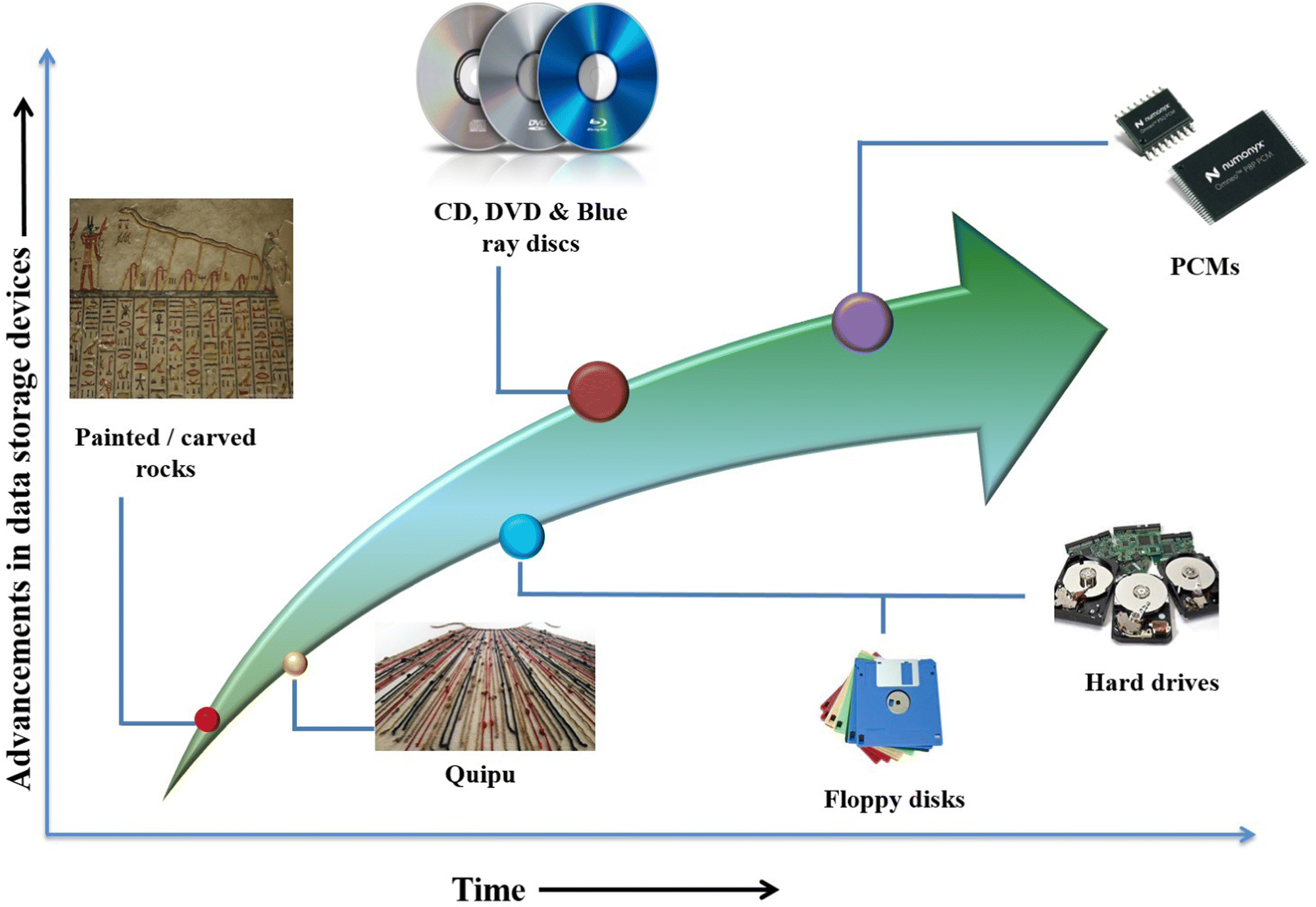 | ||
| Fig. 1 Evolution of data storage devices over a period of time. | ||
As the switching mechanism is based on the transition between two distinct phases, it is desired that both phases possess good stability to perform stable read and write operations. A low value of melting temperature (Tm) of the GST composition makes it useful in the data storage industry as it will consume low power for SET and RESET functions. A sufficient contrast provides better protection against inadvertent errors during the operation of these devices. GST has the additional benefit of better cycling ability and high endurance of stored data.91,92
The present review article attempts to summarise and systematically present the effect of dopants on various properties of GST. This systematic study of doped GST reveals a trend and a connection between different dopants by considering an entire family of similar materials, which will help to select a more precise and optimized composition as per the need for various applications. This review paper will discuss about the PCMs in brief in Section 2. Furthermore, various compositions of the GeSbTe alloy as a phase change material are discussed in Section 3. Section 4 covers the structural arrangement of atoms in GST in its different phases. To this date, GST-based PCMs face several challenges, which are discussed in Section 5. The dopants have a significant effect on the structure and bonding in GST, the detailed study of which is presented in Section 6. Similarly, the crucial effects of the dopants on the electrical and optical properties of GST are discussed in Sections 7 and 8, respectively. The irradiation effects of different types of ions on the various properties of pure and doped GST are discussed in Section 9. Further, Section 10 discusses the different applications of doped GST due to the alteration in its properties.
2 Phase change materials
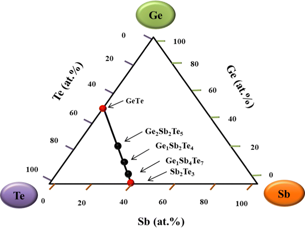
PCMs possess different phases depending upon the various thermodynamic parameters, making them valuable from the application point of view. PCMs have many applications in various fields, but these are widely utilized in the industry of memory devices.93–95 A crucial parameter which decides the utility of these PCMs in the data storage industry is if they are made to perform well read and write functions over a practical temperature range. Among the two basic processes in phase change, the crystallization process determines the data rate, whereas the amorphization process decides the power consumption.6,96 Switching between phases is induced in these materials by applying either a laser pulse or a current pulse. The choice of the pulse depends entirely on the application for which the PCM is to be used.6,97Dr S. R. Ovshinsky discovered the reversible switching mechanism for oxide- and boron-based glasses.5 He reported that the alloys consisting of elements from the III, IV, and V group combined with Te and As elements also displayed the reversible switching behaviour but did not show any data storage effects. Later, the memory effect was observed in the alloys with low concentrations of arsenic which triggered the exploration of these PCMs for data storage applications.5 The breakthrough for PCMs was attained when Yamada et al.92 discovered the range of alloys on the pseudo-binary tie-line between GeTe and Sb2Te3 alloys (indicated in Fig. 234). This led to an advanced version of rewritable devices, as these materials showed a considerable contrast between the two phases. Most of the compositions of alloys for rewritable devices belong to the compositions lying on the pseudo-binary tie line.
 | ||
| Fig. 2 Pseudo-binary tie line of GeTe and Sb2Te3 with ternary compositions (Ge2Sb2Te5, Ge1Sb2Te4, and Ge1Sb4Te7) lying between them.34 | ||
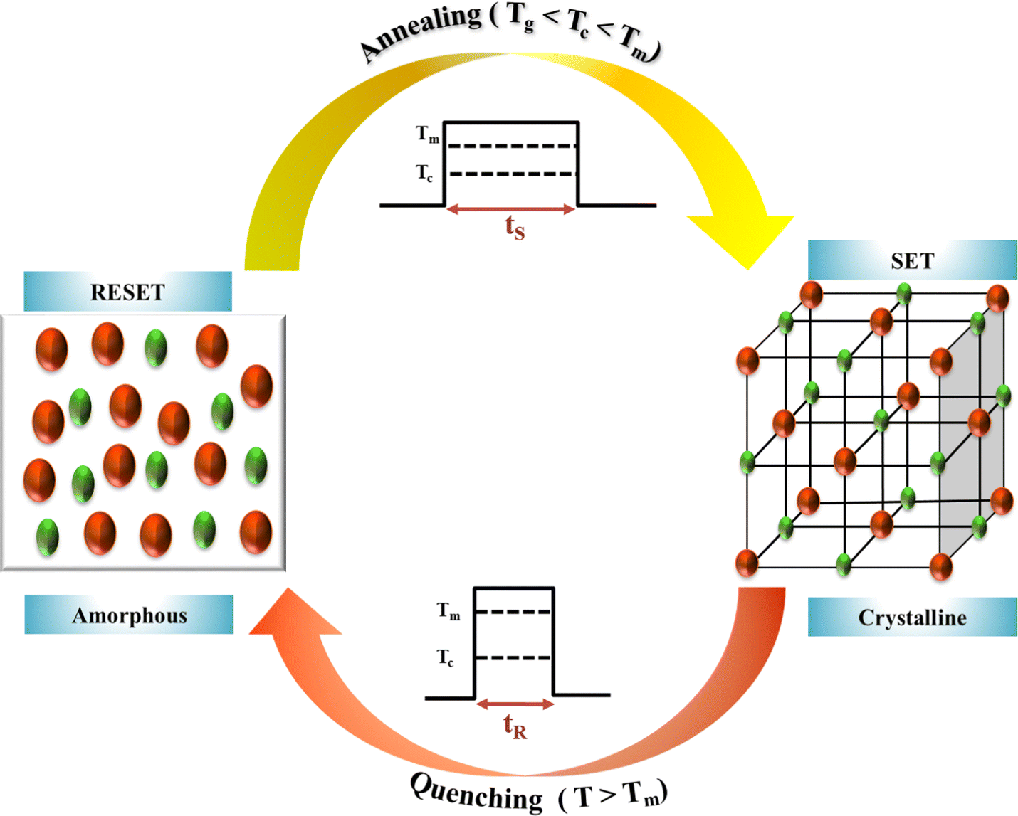
The first-ever company that introduced a product based on PCMs was Matsushita Electric (Panasonic Corporation) in 1990, and the product had 500 MB data storage capacity. These above findings ushered in the exploration of PCMs in optical memory devices, reflected in the numerous patents in this domain from various companies like IBM, Intel, Samsung, and many others. However, to utilize these PCMs to their maximum potential, the focus of researchers is now shifting to the understanding of primary switching mechanisms in PCMs.91Fig. 3 shows the basic process of SET and RESET through the process of annealing (Tg < Tc < Tm) and quenching (T > Tm) in these PCMs respectively.
 | ||
| Fig. 3 Schematic of phase transition between amorphous and crystalline phases. The red and green spheres represent the atoms. Tm is the melting temperature, Tc is the crystallization temperature, Tg is the glass transition temperature, tS is the time taken for the SET state, and tR is the time taken for the RESET state. | ||
3 GeSbTe alloy
In the late 1990s, various researchers showed interest in studying the GeTe–Sb2Te3 pseudo-binary tie line, as the alloys lying on this line were expected to exhibit “a facility for rapid crystallization”, unlike other chalcogenide alloys, which generally have “a facility for rapid amorphization”. The compositions lying on it showed a significant optical contrast, prompting many researchers to investigate further the compositions lying on the pseudo-binary tie line for their application in rewritable memory devices.34Fig. 4 represents the pseudo-binary phase diagram and the phase transition temperature of the various compositions lying on it.98 It is more interesting to know that the compositions deviating from the tie line showed a much larger delay in switching between the two phases than those lying on it. | ||
| Fig. 4 The pseudo-binary phase diagram of GeTe–Sb2Te3 and the phase transition temperature of various compositions lying on it. Adapted with permission from ref. 34. ©1991 American Institute of Physics. | ||
The crystallization temperature (Tc) increases monotonically as GeTe content increases along the tie line from the composition Sb2Te3. Ternary compositions, which lie between the two extreme binary compositions on the tie-line, exhibit a similar structure with planar layers under a regular fcc stacking rule: -a-b-c-a-b-c- which will, in turn, lead to hexagonal lattices. In thermal equilibrium, Ge2Sb2Te5 has nine cyclic layers: –Te–Sb–Te–Ge–Te–Te–Ge–Te–Sb–, Ge1Sb2Te4 has 21 cyclic layers: –Te–Te–Sb–Sb–Te–Te–Ge–Te–Te–Sb–Sb–Te–Te–Ge–Te–Te–Sb–Sb–Te–Te–Ge– and Ge1Sb4Te7 has 12 cyclic layers: –Te–Sb–Te–Te–Sb–Te–Ge–Te–Sb–Te–Te–Sb–.34,99,100 One of the reasons reported for the rapid phase transition between the two stable phases is the similarity between the symmetry of atomic distribution in the rock-salt structure and the amorphous structure.34
It is noted that the properties of PCMs changes continuously on moving along the pseudo-binary tie line from one binary composition (GeTe) to another binary composition (Sb2Te3). This is due to the continuous change in the stoichiometric composition of the alloys lying on the pseudo-binary tie-line. On moving from GeTe to Sb2Te3, the thermal stability of stored data, activation energy, glass transition temperature, and melting point decreases while the crystallization speed increases. This is attributed to the change in the atomic arrangement of the lattice due to alteration of composition.103,104 It is the average coordination number of atoms in a material that decides its ability to form an amorphous state. Usually, systems with a coordination number in the range of 2–3 (preferably 2.45) exhibit an excellent ability to be amorphous. The binary composition GeTe has a lower tendency to be in an amorphous state as its coordination number is 3. On the other hand, the coordination number of another binary composition of the pseudo-binary tie line, i.e., Sb2Te3, is approximately 2.4, hence forming a stable amorphous state.104 In the GeTe system, due to the presence of excess vacancies, the Fermi level moves to the region of extended states, so it exhibits metallic behaviour. For the middle part of the pseudo-binary tie line, vacancy-rich compositions have the Fermi level in the region of localized states, so GeSbTe compositions exhibit insulating behaviour.103,105
Amongst all the compositions present on the pseudo-binary tie line, the stoichiometric composition GST is extensively studied due to its fast phase transition speed, reversible switching, and better data retention ability over a wide temperature range.42,106–109 It has a stable phase contrast between optical reflectivity and electrical resistivity in both phases. Its high number of reversible cyclic phase transitions for at least ten years in non-volatile storage devices and computing applications impassioned many researchers to probe its properties further to enhance its features.110
4 Structural properties of Ge2Sb2Te5 thin films
4.1 Compositions lying on the pseudo-binary tie line
The binary composition GeTe is considered as the most facile composition among the other compositions lying on the pseudo-binary tie line. This binary composition exhibits the distorted rock-salt structure or, more specifically, rhombohedral structure with space group R3m.104 In this phase, both Ge and Te are 6-fold coordinated in a way known as Peierls distortion.111 It is reported by Fons et al.112 that at a Curie temperature of 705 K, the structure of the composition GeTe changes to the rock-salt structure (Fm![[3 with combining macron]](https://www.rsc.org/images/entities/char_0033_0304.gif) m). But an analysis by extended X-ray absorption fine structure (EXAFS) and pair-distribution function revealed that the structure remains the same at temperatures through the Curie temperature. It is just that the bonds in the rhombohedral structure become slightly random after the Curie temperature, so on average, this deformation looks like a rock-salt structure when probed with long-range average probe techniques such as Bragg diffraction, as discussed in chapter 46 of the book entitled “Springer handbook of electronic and photonic materials”.113 Petrov et al.114 were first to investigate the structural information of the compositions based on GeSbTe alloy and introduced the stacking sequence. Although other types of stacking sequences are also reported for GST thin films based on models such as the Kooi model, inverted Petrov model and Ferro model, they are still under debate. As reported by Li et al.,23 the Kooi model gives the most stable structure of GST composition, as depicted by density functional theory. In the Kooi model, the GeTe sublayers are integrated into the Sb2Te3 sublayers, whereas in the Petrov model, the GeTe sublayers lie outside the Sb2Te3 sublayers. In the inverted Petrov model the sequence is reversed as compared to the Petrov model, so resulting in additional van der Waals (vdW) gaps, and in the Ferro model, the GeTe bilayer follows the ferroelectric sequence.23
m). But an analysis by extended X-ray absorption fine structure (EXAFS) and pair-distribution function revealed that the structure remains the same at temperatures through the Curie temperature. It is just that the bonds in the rhombohedral structure become slightly random after the Curie temperature, so on average, this deformation looks like a rock-salt structure when probed with long-range average probe techniques such as Bragg diffraction, as discussed in chapter 46 of the book entitled “Springer handbook of electronic and photonic materials”.113 Petrov et al.114 were first to investigate the structural information of the compositions based on GeSbTe alloy and introduced the stacking sequence. Although other types of stacking sequences are also reported for GST thin films based on models such as the Kooi model, inverted Petrov model and Ferro model, they are still under debate. As reported by Li et al.,23 the Kooi model gives the most stable structure of GST composition, as depicted by density functional theory. In the Kooi model, the GeTe sublayers are integrated into the Sb2Te3 sublayers, whereas in the Petrov model, the GeTe sublayers lie outside the Sb2Te3 sublayers. In the inverted Petrov model the sequence is reversed as compared to the Petrov model, so resulting in additional van der Waals (vdW) gaps, and in the Ferro model, the GeTe bilayer follows the ferroelectric sequence.23
GST has a stable hcp crystal structure with space group Pm1 and a stacking sequence of Te–Sb–Te–Ge–Te–Te–Ge–Te–Sb–Te along the c axis as per the Petrov sequence.114 It was later found that the layer consisting of Ge/Sb atoms was involved in the random occupation of these two elements.115 Further studies performed by Yamada et al.116 on the stoichiometric composition GST disclosed the metastable rock-salt crystal structure with space group Fmm. This phase lies in between the amorphous and the stable hcp phase.108,109 The rocksalt phase consists of two sublattices: (i) anionic sublattice, which is fully occupied with Te atoms, and (ii) cationic sublattice, which is partially occupied with Ge/Sb atoms along with 20% vacancies.113 Usually, Ge undergoes sp3 hybridization, but the situation is changed when Ge bonds to Te, which is a chalcogen atom. The outer shell of the Te atom consists of two unpaired and one non-bonding lone pair; hence it forms two covalent bonds as Ge–Te. In addition, it also includes a two-electron dative bond with the empty p-orbital of unhybridized Ge, which is usually indistinguishable from covalent bonds, resulting in a coordination number of 3 for Ge. As the element Sb is incorporated into GeTe, Sb atoms form two covalent bonds with Te atoms leaving a lone pair on the Te atoms. It implies that two Sb atoms replace three Ge atoms leaving one vacant site, which causes the 20% vacancies in the GST alloy. Hence, Te is 2-fold coordinated when bonded to Sb, leading to the placement of three Te atoms next to the vacancy, which enables Te atoms to move quickly or change their direction with an increase in their bonding with Sb which is discussed by Kolobov et al. in chapter 46 of the book entitled “Springer handbook of electronic and photonic materials”.113 This is why GST films possess three different structures over a different range of temperatures. Thin films of GST exhibit metastable rock-salt structure when annealed in the temperature range of 150 °C to 170 °C. On further increasing the temperature (above 230 °C) their phase changes to the hcp phase.97,108,109
4.2 Amorphous phase of Ge2Sb2Te5 thin films
An understanding of the structural arrangement of atoms in the amorphous phase of GST is essential to unravel its behaviour under different thermodynamic conditions. The evaluation of the structural arrangement of atoms in the lattice is hard to analyze in the amorphous phase as compared to the crystalline phase because there are only very few experiments that can provide information on such a short-range atomic order. Various researchers have investigated the structural order of atoms in the amorphous phase, and many are still exploring it with great enthusiasm in more detail. For the amorphous phase generally, the structure is probed by using X-ray techniques providing radial distribution function (RDF).117 Furthermore, transmission electron microscopy with electron diffraction is an effective method for analysing the structure of nanostructured materials because of its high magnification, which allows individual atoms to be seen.118–120 All other compositions of the GeSbTe alloy have less tendency to form an amorphous state when compared to Sb2Te3. Since GST lies in the mid of the pseudo-binary tie-line, its tendency to form an amorphous phase lies between that of Sb2Te3 and GeTe.103 The LETI group (Laboratory of Electronics Information Technology) in France was the first to report the local structure of the amorphous phase of GST alloys.94,121 They observed that the amorphous phase has shorter bonds than the crystalline phase. Kolobov et al.94 proposed structural models for the amorphous phase and observed a shortening in the bond lengths of Ge–Te and Sb–Te along with more local structure ordering at a shorter range. Despite the shorter bond length, density for the amorphous phase is 5% lower than that of the crystalline phase. GST thin films in the amorphous phase were reported to have homopolar Ge–Ge bonds, which stabilize this phase and whose fraction is similar to the concentration of tetrahedral Ge sites.113 Among various occurring unexpected or wrong bonds (bonds which are absent in the widely accepted model of the metastable cubic structure like Ge–Ge, Sb–Sb, Ge–Sb, and Te–Te), bonds like Ge–Ge and Ge–Sb were found to be present in a significant number.122 The amorphization of GST thin films is due to the jumping of Ge atoms from octahedral to tetrahedral position, which is popularly known as umbrella flip.94 This flip is one of the possible dynamics for the phase switching mechanism. There are also other explanations which are still under debate for the phase change between the amorphous and the crystalline phase like the Poole-Frenkel mechanism.123Fig. 5 shows the change in the bonding between Ge and Te atoms, i.e., from sp3 type to p-type bonding, and the umbrella flip of Ge atoms. The weaker covalent bonds shown by thin lines rupture when an intense laser pulse is applied to a crystallized thin film, leading to umbrella-flip. It should be noted that three solid covalent bonds remain intact during the melting process. This is why the phase switching is fast and stable in GST alloys. | ||
| Fig. 5 (a) The valence alternation process between Ge and Te. In 3D space, the sp3 bonds have a tetrahedral shape with a bond angle of 109°, while the p bonds are perpendicular to each other. The valence alternation changes not only the coordination number of Ge and Te, but also the bond angle around Ge. Adapted with permission from ref. 101. ©2009 American Physical Society. (b) Fragments of the local structure of GST around Ge atoms in the crystalline (left) and amorphous (right) states. Adapted with permission from ref. 94. ©2004 Springer Nature. | ||
But to reveal the structural information of the amorphous phase, a specific technique alone is not sufficient because of the short-range ordering of the atoms. A simulation study conducted by Jovari et al.122 through Ge K-edge EXAFS also supported the presence of homopolar Ge–Ge bonds in the amorphous phase, which was also later endorsed by other research groups. Furthermore, research on the amorphous phase of GST showed that unexpected bonds like Sb–Ge and Ge–Ge were present in a significant number, but bonds like Te–Te and Sb–Sb were absent. All GST atoms in this phase obey the ‘8 − N’ rule for coordination, where N is the number of valence electrons in the atom.122
The short-range atomic arrangement can vary significantly with the method used for thin film deposition. So, for the same stoichiometric composition, there can be many different amorphous phases with variable properties. The as-deposited amorphous GST (a-GST) thin films showed an abundance of homopolar Ge–Ge and Te–Te bonds when examined with EXAFS and Raman spectroscopy measurements.117 As calculated from ab initio molecular dynamics simulations, Ge atoms showed diverse behaviour in a-GST thin films. Some Ge atoms may sustain the sp3 hybridization with tetrahedral configuration (CN = 4), while most of the Ge atoms suffer valence alteration when bonded to Te atoms, which in turn destabilizes the sp3 hybridization and promotes p-type bonding among them. This p-type bonding changes the bond angle around Ge atoms to 90° and the coordination number of Ge and Te atoms to three.101
4.3 Structure of crystalline Ge2Sb2Te5 thin films
GST has a rocksalt metastable phase in which one sublattice consists of 40% Ge, 40% Sb, and 20% vacancies at the cationic site, and the other sublattice consists of Te atoms at the anionic site.24 All the phase change alloys possess local distortions to some extent, and notably, the degree of crystal lattice distortion depends upon the number of vacancies in the cation sublattice. Since Ge and Sb are off-centred within idealized Te(GeSb)6, lattice distortions are more pronounced in GST than in any other chalcogenide-based compositions. Within an individual cationic layer, Ge and Sb atoms are randomly distributed. However, there is still an ordered arrangement among Sb atoms in the cation layer, which is present next to the vacancy layer, and Ge atoms are present in the middle of the GST building units. The degree of vacancy ordering strongly depends upon the distance between Te–Te atoms.1244.4 fcc phase of Ge2Sb2Te5 thin films
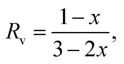
The phase transition for GST alloys always occurs between the amorphous and metastable fcc phase. No matter whether the GeSbTe alloy is Ge rich or Sb rich, the fcc phase always appears initially before the hcp phase whenever crystallization occurs. When Tc is increased, first, the metastable fcc phase appears, then it changes to hcp at higher temperatures. The fcc phase consists of two sublattices: (i) anionic sublattice, fully occupied with Te atoms, and (ii) cationic sublattice with randomly occupied Ge and Sb atoms along with 20% vacancies. The ratio of the vacancy, Rv, is approximated bywhere (1 − x) is the concentration of Sb2Te3, when the composition is expressed by (GeTe)x–(Sb2Te3)1−x. Typically, in the case of GST, where x is equal to 1/3, Rv gives the value of 20% at the cationic site.125 In GST composition, excess of Ge and Sb atoms instead of occupying vacancies were found to assemble near grain boundaries.71,84 Zhang et al.102 further probed about the sublattice structure of crystalline GST thin films in detail at the atomistic level using high angle annular dark-field scanning transmission electron microscopy (HAADF-STEM), which reveals that the brightness of the atomic column is proportional to their atomic number (Z) as Z2. So, this sophisticated imaging technique reveals the atomic arrangement of Ge, Sb, and Te atoms and vacancies in the metastable phase of GST thin films. Fig. 6 shows the results of HAADF-STEM GST thin films in the fcc phase where the bright dots represent whole atomic columns along the viewing direction. The brightness of these dots is approximately proportional to Z2. Atomic columns in Fig. 6e and f exhibit two types of sublattices: one sublattice corresponding to the uniform bright spots is reported to be due to the heavier Te atoms. Another sublattice consisting of dark spots is caused by atoms like Ge and Sb along with vacancies arranged in a random manner.102,126–128
 | ||
| Fig. 6 Atomistic models and STEM-HAADF images of rocksalt GST. Adapted with permission from ref. 102. ©2016 American Institute of Physics. | ||
4.5 Hexagonal phase of Ge2Sb2Te5 thin films
The stable hexagonal hcp phase forms on annealing GST thin films above Tc for the fcc phase but well below the melting temperature. This phase of GST consists of alternating blocks of Ge/Sb and Te layers which are bound together by weak van der Waals forces.108,109 As per the Kooi model, the stable phase was observed to have a stacking order of Te–Ge–Te–Sb–Te–Te–Sb–Te–Ge– in the [0001]-direction. But as this stable structure has alternating blocks of Sb2Te3 and GeTe, the phase transition actually takes place between the amorphous phase and the metastable fcc phase of GST thin films.6,100,129,1304.6 Switching in Ge2Sb2Te5 thin films
The ability which makes GST thin films unique among all their counterparts is their fast and stable switching property between amorphous and crystalline phases. The phase change in these thin films is very fast (of the order of 50 ns) as compared to other materials (of the order of 100 ns).103 The phase transition can be induced by applying any electrical, optical, or laser pulse. Fig. 7 shows the switching between different phases of GST thin films. The atoms can easily switch between these phases because of the isotropic distribution of atoms in the amorphous phase and its similarity with the lattice in the fcc phase. | ||
| Fig. 7 Schematic diagram of phase transition between different phases of GST. The red, yellow and blue spheres represent Te, Ge, and Sb atoms, respectively. | ||
Shinji et al.131 used the reverse Monte-Carlo simulation technique along with experimental data from synchrotron radiation XRD. They showed that the presence of an even folded ring structure in the amorphous phase plays an essential role in the rapid crystallization as it corresponds well with the crystalline phase of GST. The factor responsible for the transition from crystalline to amorphous phase is the rapid quenching time of GST, which is around 1 ns to 10 ns. In contrast, crystallization of GST requires a longer time for annealing, i.e., around 100 ns.103 The local environment of the amorphous phase is more ordered than that of the crystalline phase, albeit over a much shorter distance.
On melting the crystalline thin films, intra-block bonds become shorter and more robust due to the rupturing of inter-block bonds (longer Ge–Te and Sb–Te bonds). Ge atoms change their symmetry position from octahedral to tetrahedral with phase change from an ordered to a disordered arrangement through the umbrella-flip of Ge atoms.94
Phase transition also involves the change in electronic states, including the shift of hybridization from p-type to sp3 hybridization in crystalline to the amorphous phase, respectively. On the other hand, the local environment around Sb atoms remains unchanged during the transition process, accounting for overall structural stability.94 When these two phases were compared, the following interesting characteristics were discovered:
1. Both phases are formed by –Ge(Sb)–Te– alternative rings with a similarity in their bond angle, and
2. The presence of a large number of 4- and 6-fold rings of GeTe is responsible for the high thermal stability of the amorphous phase.
Fig. 8 shows the possible changes in the ring size with phase transition. The pseudo-network formation by Sb–Te bonds is responsible for faster crystallization.125 Therefore, as the Ge concentration decreases on moving along the pseudo-binary tie line from GeTe to Sb2Te3, it is easy to obtain a stable hcp phase at low temperatures.
 | ||
| Fig. 8 Schematic representation of the possible ring size transformation in crystal–liquid–amorphous phase change (record) and amorphous–crystal phase change (erase) in GST. Stage I and II: recording process in optical storage; stage III: erasing process in optical storage. Adapted with permission from ref. 131. ©2006 American Institute of Physics. | ||
5 Challenges for Ge2Sb2Te5 thin films
Despite possessing numerous superior features, stoichiometric composition GST still has several constraints that hinder its use in the data storage industry. These bottlenecks include the high value of Tm, high activation energy, and relatively low Tc. The need for fast crystallization speed as well as the good thermal stability of the amorphous phase seems contradictory, but these properties are simultaneously desired in modern technology. So, there is a search for a novel composition of the chalcogenide-based alloy which can simultaneously preserve these properties. This need for novel composition provides room for either tailoring the host lattice or adding dopants from various groups in this chalcogenide-based alloy composition. To date, many periodic table elements have been doped in GST thin films to make it ideal for various applications. To predict the structural and thermal properties, the knowledge of kinetic parameters is very crucial. Specific dopants can tune these parameters to improve the properties of GST thin films. Various elements have been doped into the host GST composition, among which p-block and TM elements play a significant role. Understanding the fundamental physics behind the alteration of various properties due to doping and annealing is necessary to utilize the potential of this material to its fullest.6 Effect of dopants on the structure and bonding of Ge2Sb2Te5 thin films
It is crucial to investigate the effect of several types of dopants on the structure and bonding of GST thin films so that these can be grouped according to their effect. When added in low concentration, doping elements belonging to the TM group do not restrict the crystallization speed of the host GST material. In the simulated annealing treatment, it is reported that TM-doped GST (TM-GST) leads to switching between the amorphous and fcc phase by suppressing the stable hcp phase. Also, analyzing the adopted crystalline models in energy relaxed mode did not lead to the formation of the hcp phase. Hence, it can be inferred that the TM dopants inhibit the formation of the hcp phase and hence lead to the single-step crystallization between the amorphous and fcc phase.132 This will be helpful in reducing the power consumption by lowering the RESET current. Also, the effect of doping elements belonging to the p-block has been widely explored to enhance the properties of the host GST. It is noted that doping of N,133,134 C,135 O,136etc. helped in altering the properties of GST thin films to a considerable extent. Most of these p-block dopants are reported to strengthen the thermal stability of the amorphous phase of GST by enhancing the value of Tc.6.1 Effect of transition metal dopants
Doping transition metal elements into GST is of extensive research interest as it imparts remarkable property enhancement to the host lattice. It is noted that first-row TM elements form either a tetrahedral or octahedral coordination, therefore affecting the structural arrangement of the host GST lattice. Doping these elements in low concentration did not affect the crystallization rate of host GST thin films as studied by first-principles computer calculations. Instead, doping suppressed the hcp phase by stabilizing the metastable fcc crystalline phase when annealed at a temperature much higher than the phase transition temperature but well below its Tm. These TM-doped GST thin films acquire a flexible range of geometries due to the presence of 20% octahedral vacancies at the cationic sublattice in the metastable fcc phase, these vacancies cluster themselves to provide larger voids where doping elements can reside.132 The low-Z transition metal ions tend to occupy cationic sites, while the high-Z one prefers to occupy the interstitial sites; the ones in between can occupy both octahedral and interstitial sites. Hence in the amorphous phase, among the first-row TM elements, Sc, a low Z element, occupies the cationic site, whereas elements like Ti, Cr, and Co can occupy both octahedral and interstitial sites and elements like V and Fe prefer to settle in the interstitial site. Further, higher Z elements (Ni, Cu, Zn) take up the interstitial sites and may position themselves near the grain boundaries.132 Therefore, it can be inferred that elements present on the right of the TM elements series prefer to locate near grain boundaries as atomic size reduces on moving across the period from left to right. Hence, they tend to accommodate large voids and form complexes with atoms at the edge of defects.Various researchers reported a general reduction in the bond length in doped GST thin films on moving from Sc to Co as the nuclear charge per electron increases. However, Ni, Cu and Zn do not exhibit this decreasing trend as they are likely to have different geometries. Most TM elements prefer to bond with Te due to their natural inclination towards interstices, except for Co and Ti, which showed affinity to bond with Ge and Sb atoms.57,137,138 From the reported study, it is found that moving from left to right in the first row of TM elements led to the change in energy of the d-states from within the conduction band to deep within the valence band.132 Hence these dopants will help to alter the bandgap and affect the optical and electrical contrast of GST thin films.
TM elements like Ni, Cu, and Zn, whose bonding geometry does not match with the metastable cubic structure, tend to settle near voids and grain boundaries forming complexes. This causes minimal distortion in the crystal structure and therefore suppresses the fcc to hcp phase transition.132
On the other hand, elements on the right side of the TM series prefer to take non-octahedral geometry due to the reduction of the atomic size with increasing nuclear charge. Hence moving across the period from left to right led to the change in geometry from octahedral to tetrahedral coordination, as shown in Fig. 9.132
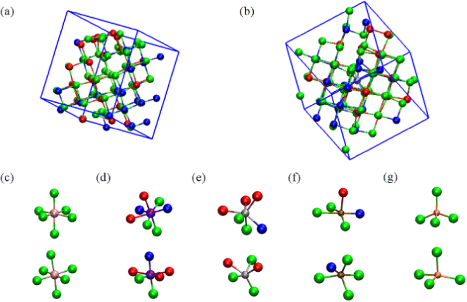 | ||
| Fig. 9 Structure and bonding in transition-metal (TM)-doped Ge2Sb2Te5. (a) Sc-, (b) V-, (c) Cr-, (d) Co-, (e) Ni-, (f) Cu-, and (g) Zn-doped GST in amorphous (top) and crystalline (bottom) models. The green, red and blue balls represent Te, Sb, and Ge atoms, respectively. Adapted with permission from ref. 132. ©2006 IOP. | ||
One such study by Gao et al.45 on the thermal stability and microstructure of Cu doped GST (Cu-GST) thin films revealed that the doped system exhibits high thermal stability than the undoped one. In Cu-GST thin films, Cu has the least electronegativity value among the other compositional elements (Ge, Sb, and Te), so Cu was expected to enhance the crystallization speed by reducing the binding energy among the host atoms. Doping of Cu led to no separate segregated phase, but when the hcp phase becomes the dominant phase, then a new diffraction peak at 24.57° was observed in the XRD pattern of Cu13.7(GST)86.3. This new peak signified the new bond formation of Cu–Te, but due to its relatively weak intensity compared to other bonds, this new bond formation induced no phase segregation. The switching speed of these doped thin films was reported to get enhanced due to the presence of sharp fiber texture when annealed at 370 °C. This surface intensity was reported to improve along with increasing Cu content in GST thin films. The thickness study of Cu-GST thin films by X-ray reflectivity (XRR) technique revealed that the thin film thickness contrast between the stable phases decreases considerably with increasing doping concentration, strengthening their cyclic endurance. It was reported that the Tc in Cu-GST had shifted to a higher value, and its amorphous phase was stabilized. Therefore, the Cu dopant acted as a thermal stabilizer for the amorphous phase. A study through X-ray photoelectron spectroscopy (XPS) showed that the binding energy of Cu increased as the doping concentration was increased. It was reported that there is an increment in Sb–Te bond dissociation and Cu–Te bond formation along with promotion in the Ge–Te bond which resulted in the enhanced thermal stability of Cu-GST.
Wang et al.50 investigated the structural, thermal, optical, and electrical properties of Zn doped GST (Zn-GST) thin films deposited by magnetron co-sputtering. The researchers were interested in Zn doping because it exhibits a weak bonding strength with Te and hence can lead to the fast crystallization speed for phase transition. The reported study concluded that with a gradual increase in Zn doping concentration, the crystallization temperature significantly shifted to a higher value, providing high thermal stability to the amorphous phase. Doping of high Zn concentration placed a restriction on fcc-to-hcp phase transition as the Sb–Te bond which is mainly responsible for phase transition from fcc to hcp phase got replaced by Zn–Te and Zn–Sb bonds, leading to a one-step crystallization between amorphous and fcc phases.50 Wei et al.46 worked on Ti-doped GST thin films because the Ti element is generally used in phase-change random access memory (PCRAM) cells as an adhesion layer, so this could affect the storage performance straight away. Thin films of Ti-doped GST were deposited by the DC co-sputtering method at a working pressure of 8 × 10⁻³ mbar at room temperature. They observed that with an increase in the Ti doping concentration, the value of Tc increased, signifying the delay in phase transition upon incorporating Ti into GST thin films. With a further increase in Ti doping concentration, the dormancy in the change in reflectivity of thin films indicated the contribution of Ti in restraining the phase transition from fcc to hcp phase. Thus, the metastable fcc phase exhibited high thermal stability owing to the Ti dopant addition. A study of the XRD results revealed that the crystallization state had remained almost identical for Ti-doped GST thin films with a Ti concentration of 1.23% when annealed at 260 °C and 400 °C. The XPS study concluded the existence of the new bond between Ti and Te in the Ti-GST film, which was the reason behind the restraint effect in the fcc to hcp phase transition.46
From the reported literature, it is found that Ag also acted as a potential dopant choice in GST composition. It increases the reflectivity of GST thin films and possesses a high solubility in chalcogenide semiconductors, so it helps to tune optical properties to a significant extent.52,139 Singh et al.18 reported a phase transition from amorphous to hcp phase at a much lower temperature for silver doped GST (Ag-GST) as compared to the undoped host and so suggested a reversible NIR window at a lower temperature.18,53 It was demonstrated that for 5% of Ag concentration in the host GST, the fcc phase dominates, but for 10% Ag content, the hcp phase dominates at 160 °C. This indicated that Ag doping lowers the temperature for hcp phase transformation. This finding was further supported by scanning electron microscopy (SEM), which revealed that the Ag dopant with a concentration of 10% possesses similar morphology for both the annealing temperatures, i.e., at 160 °C and 260 °C. In conclusion, these results indicated that the Ag dopant promotes nucleation and growth of crystallites. Increased Ag doping concentration in the host GST induced distortion in the lattice and hence at a lower temperature, composition (Ge2Sb2Te5)90Ag10 has similar structural and optical properties to the hcp phase of the undoped GST.18
Guo et al.42 did a systematic study on the effect of tungsten doping in the host GST (W-GST) thin films. Using the co-sputtering method, they deposited the thin films on two different types of substrates, i.e., silica glass and silicon substrates. The silica glass substrate was used to determine electrical properties and for XRD studies, while the Si (100) glass substrate was used for thermal conductivity measurements. Due to the similar atomic radius of W (∼210 pm) and Ge (∼211 pm), these dopant atoms may act as a substitutional impurity in the crystal lattice of the host GST. Also, another possibility is that W can act as a p-type dopant by serving as an acceptor to Ge atoms. With 4% of W doping in GST thin films, a reduced resistivity contrast by one order of magnitude was noted under set deposition conditions, i.e., RF power on the GST target at 100 W and fine-tuning the DC power on the tungsten target as well as placing different mesh sizes. W-GST thin films remained in the fcc state up to 350 °C, whereas undoped GST switched to the hcp state beyond 300 °C, so the doped composition provided a broader range of operation by suppressing the hcp phase. It is difficult to reverse a stable hcp phase compared to the metastable fcc phase back to the amorphous state due to the requirement of a high crystallization temperature. Hence W-GST thin films have the potential to lower the power consumption by reducing the writing current.
Doping of small-sized post-transition elements, such as Al, in GST thin films exhibited no noticeable trend in Tc with different Al doping concentration. Along with the increase in Al doping concentration, a non-uniform trend was observed for the value of Tc; initially, it decreased, then increased and then again decreased. This sporadic trend implied that Al at first acted as a network modifier and then as a network maker in the Al-doped GST (Al-GST) lattice network, i.e., following a similar trend as in the case of Ag-doped GST thin films. Al-doping restrained the formation of crystalline grains and exhibited no hcp phase up to a temperature of 400 °C. Hence, Al-GST exhibited one-step crystallization between amorphous and fcc phases.72,73 According to Wang et al.,76 doping of indium in Ge2Sb2Te5 thin films slowed down the incubation time by 150 ns when compared to undoped ones. These doped thin films have a thickness of 70–120 nm and were heated up to a temperature of 250 °C, with a heating rate of 2.5 °C min−1. As observed from the power time effect (PTE) diagram, there was a sharp boundary between the two regions. The position of this boundary with respect to the time axis is called incubation time. The delay in the incubation speed was speculated due to the segregation of In2Te3 in the metastable (fcc) phase of GST thin films.76,77
The suppression of the hcp phase was also observed for nitrogen-doped GST (N-GST) thin films. The doping increased the crystallization temperature and further phase transformation temperature for fcc to hcp phase transition. Nitrogen doping prompted the formation of Ge–N bonds, which suppressed the grain growth in the nitrogen-doped system. Probing through the AFM images of various N-GST thin films revealed that with lower doping concentration, the surface roughness of thin films decreases. But a further increase in N doping also resulted in the emergence of small hillocks. These hillocks were reported due to the presence of nitrides at the grain boundaries, so they resulted in surface roughness as a whole.61,62
Researchers also showed interest in studying the arsenic doped GST system due to its good glass formation ability. Also, the chemical reactivity and valence electronic configuration of arsenic are similar to Sb. So, arsenic atoms are expected to substitute the Sb atoms, but the similarity of its atomic radius and atomic mass with Ge makes it probable to substitute Ge sites also. Therefore, arsenic was considered as a potential choice to influence different properties of GST based on its variable site occupancy in the host matrix. The atoms of arsenic can either occupy vacancies and interstitial sites or substitute the lattice sites of constituent atoms. Motivated by this, various researchers showed interest in studying arsenic-doped GST thin films. Madhavan et al.59 published their work on arsenic doped GST thin films and revealed that arsenic doping enhanced the thermal stability of GST because of the requirement of higher annealing temperature for phase transition than the undoped one (150 °C). It was concluded that the proportional insertion of arsenic atoms in the host GST composition led to the enhancement of tetrahedral character. In contrast, substituting Sb atoms with arsenic atoms decreased the tetrahedral character of the network. The significant resistivity contrast of arsenic-doped GST thin films in the crystalline and amorphous phase improved the data retention ability and reduced the writing current.59
On the other hand, doping of Sb into GST resulted in suppression of the fcc phase. By altering the coordination number, it led to one-step crystallization between the amorphous and hcp phase. On the other hand, excess of Sb added into GST had changed the stoichiometric composition to Ge15Sb47Te38 with a reduction in Tm by 70 °C, which will tackle the issue of high power consumption by GST thin films. Sb-GST had changed the crystallization mechanism from nucleation driven (an initial process of formation of the crystal from a new site) to controlled grain growth (a process of extension of the size of a pre-existing crystal structure).80,81
The stability of the amorphous phase was noted to get enhanced when dopants of the carbon family (C, Si, Ge, Sn, and Pb) were added to the GST thin films. C doping in GST thin films creates C-C covalent bonds in the network, which have a high Tm value. So this dopant shifts the Ge atom bonding from p-type to sp3 type bonding. Doping of C in GST thin films increased the odd fold rings significantly, so slowing down the nucleation and stabilizing the amorphous phase, leading to better data retention ability of doped thin films.68 Doping element Sn when added to GST (Sn-GST) thin films was reported to increase the crystallization speed by rupturing Ge–Te bonds and forming new Sn–Te bonds. The weaker binding energy of Sn–Te was responsible for this enhanced crystallization speed. Due to the large size of Sn atoms compared to that of Ge atoms, rearrangement of atoms during crystallization was impeded, resulting in a higher value of Tc.41,60 On the other hand, in simulation studies for Si-doped GST thin films, it was observed that the Si dopant increased the binding energy between the atoms by increasing the total coordination number due to its comparable size to host constituent atoms (Ge, Sb, Te). This increased coordination between atoms slowed down the diffusion of atoms which in turn retarded the crystallization process.87,88
Doping of chalcogen elements (O, S, Se, Te) into GST thin films were reported to stabilize the amorphous phase and improve the overwrite cyclability of GST thin films. As oxides like GeO2, Sb2O3, and TeO2 are generally predicted to have a high Tm value, so motivated by this, researchers doped O in GST to suppress data flow during switching between distinct phases and to enhance the data overwriting property.74 Recording sensitivity got enhanced with an increase in oxygen content in GST thin films with improved overwriting characteristics in the blue wavelength region. Also, doping another chalcogen element, i.e., Se, into GST led to one-step crystallization between the amorphous and hcp phase by suppressing the metastable fcc phase. As both Te and Se elements belong to the same group, Se doping into GST thin films promotes the –Te–Te– stacking by following either the –Te–Se– or –Se–Se– stacking pattern.58,74,75
The effects of various doping elements on the crystallization temperature and various properties of GST thin films are summarized in Table 1.
| S. no. | Doping elements | Crystallization temperature (Tc) | Changes in properties |
|---|---|---|---|
| 1 | Undoped | ∼125–160 °C97,108,109 | — |
| 2 | Tungsten (W) | 170–275 °C42 | Stabilizes the fcc phase |
| 3 | Arsenic (As) | 150–160 °C59 | Increases Tc and thermal stability |
| 4 | Copper (Cu) | 192 °C44,45 | Improves cyclic endurance as well as Tc, thermal stability enhances |
| 5 | Titanium (Ti) | 230–251 °C138,140 | T c increases along with thermal stability of the fcc phase |
| 6 | Selenium (Se) | 200 °C58 | Improves resistance contrast and one step crystallization between amorphous and hcp phases |
| 7 | Zinc (Zn) | ∼188–272 °C50 | Enhances both Tc and thermal stability of the amorphous phase |
| 8 | Tin (Sn) | ∼149 °C41,60 | Speeds up the crystallization process and increases Tc |
| 9 | Nitrogen (N) | 180 °C61–67 | Increases both Ea and Tc and suppresses grain growth |
| 10 | Carbon (C) | ∼180–224 °C68–70 | Stabilizes the amorphous phase, slows down the nucleation rate by promoting covalent bonding |
| 11 | Silver (Ag) | 210 °C18,52,54,55 | Reduces temperature for transformation from fcc to hcp phase and promotes nucleation |
| 12 | Aluminium (Al) | ∼177–220 °C73 | Suppresses fcc to hcp phase transformation and strengthens thermal stability |
| 13 | Nickel (Ni) | ∼180–217 °C141 | Minimized resistivity contrast between amorphous and crystalline phase |
| 14 | Oxygen (O) | ∼164 °C66,74,75 | T c increases, grain size decreases and Ea increases |
| 15 | Silicon (Si) | ∼160–275 °C85–90 | Reduces writing current, enhances recording stability and Tc increases |
| 16 | Antimony (Sb) | ∼200 °C81 | Induces one step crystallization between amorphous and hcp phase and strengthens thermal stability |
| 17 | Indium (In) | ∼169–256 °C77 | Enhances Tc and thermal stability |
7 Effect of dopants on electrical properties
GST-based PCMs utilize a significant resistivity contrast between their two stable phases. Usually, this contrast is depicted by plotting resistivity vs temperature. Generally, the sheet resistance of thin films is measured by a popular method known as the four-point probe. Fig. 10 shows a plot of the resistivity contrast of various compositions (GST, N-GST, GeSb, Sb2 Te, and AIST) of thin films with different annealing temperatures. Two distinct transitions can be seen clearly in the plots for undoped GST. The first transition corresponds to the amorphous-fcc phase and the second transition corresponds to the fcc-hcp phase. | ||
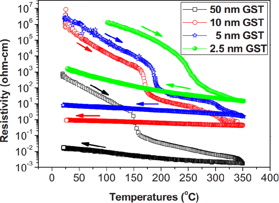
| Fig. 10 Resistivity contrast as a function of temperature for various compositions of 50 nm thin films. Adapted with permission from ref. 142. ©2010 American Institute of Physics. | ||
The properties like topological insulation, thermoelectric properties, and interfacial phase change memory strongly depend upon the growth parameters for film deposition. As per the classical theory of crystallization, the deposition rate, temperature, pressure and substrate affect the entropy and enthalpy during the process of crystallization.144 Resistivity contrast of GST thin films strongly depends upon various parameters such as film thickness, deposition methods, and heating rate.145Fig. 11 shows the trend of resistivity contrast of GST thin films with different thicknesses over a wide range of temperatures. It is evident from this figure that as the film thickness increases, both the resistivity and Tc decrease. This decrement may be due to an increase in the nucleation rate and phase segregation since the composition content also increases along with thickness.143 In addition, as the heating rate increases, Tc also increases logarithmically, but activation energy for crystallization decreases.

Different deposition methods also lead to variation in resistivity contrast, and along with this, film deposition with a particular technique but with distinct pressure conditions might also exhibit distinct resistivity contrast. Apart from that, various doping elements such as N, O, Si, W, Zn, As, Ni, etc. have been doped in GST, which exhibited a considerable effect on its electrical properties to address critical technological issues like high writing current in GST based devices. Oxygen- and nitrogen-doped GST thin films have been reported to possess a wide mobility gap and increased activation energy compared with undoped ones. This, in turn, has reduced the conductivity of O-doped GST samples. Due to the covalent nature of oxides, segregation occurred at the grain boundaries, resulting in the higher value of Tc and enhanced cyclability. Similarly, nitrogen doping induced a higher value of dynamic resistance in GST thin films, the effect of which was observed in reduced writing current. As the nitrogen atoms tend to segregate at the grain boundaries, a consequent suppression in heat diffusion is reported, resulting in more efficient power delivery.66 Kim et al.63 studied the electrical switching characteristics of N-GST thin films fabricated using the sputtering method with TiN as the top and bottom electrodes. Their results supported the trend of enhanced dynamic resistance with an increase in N doping concentration in the host GST composition.63 An increment in the sheet resistance of crystalline N-GST thin films was observed up to 12 sccm gas flow rate of nitrogen, after which the sheet resistance dropped due to the formation of large grain size in doped GST thin films. It was further concluded that nitrogen doping reduces reset power consumption and makes power delivery more worthwhile.62

 | ||
| Fig. 11 Resistivity contrast along with various thicknesses of GST thin films for a wide range of Tc. Adapted with permission from ref. 143. ©2010 American Institute of Physics. | ||
It has been found that arsenic doping in GST thin films leads to a high resistance value for crystallized thin films. This increase is expected because arsenic atoms act as scattering centres at grain boundaries, so the associated phase formation causes a structural change. As a result, the resistance increased for both deposited and annealed arsenic doped GST thin films. Hence this more prominent resistivity contrast in doped GST thin films improves the data retention capability and thus reduces the writing current.146
For Si-GST, it was found that no hcp phase was there for 11.8 at% of Si at a temperature of 460 °C. Since Si has an ionic radius comparable to that of Ge, Sb, and Te, there are chances of it replacing either host atoms or occupying the vacancy sites at cationic sublattices. Such possibilities are speculated to resist atomic diffusivity; therefore, suppression of the hcp phase indicates that the thermal stability of the fcc phase improved profoundly, boosting the recording stability. Moreover, the properties like threshold voltage Vth, resistivity, and dynamic resistance got improved with an increase in Si doping concentration. Along with that, an appreciable enhancement in recording stability is observed upon Si doping in GST, as it increased the Tc with a consequent decrease in Tm, which resulted in reduced power consumption.85 Due to the tetravalent character of Si atoms, it increases the ratio of covalent bonds, thereby widening the mobility gap. This widening in the mobility gap led to the increment in activation energy for electrical conduction. From the study of I–V characteristics, the writing current was also observed to get reduced with Si doping. This reduction was noted to be due to a decrease in the free carrier concentration and a widening of the mobility gap.88
From the reviewed literature, we have come to know that there is no other dopant except for Ni which can reduce the resistivity of the amorphous phase of GST thin films.57 So, only Ni holds the potential to minimize the resistivity contrast, leading to the fabrication of devices with high electrical switching speeds. Guo et al.57 reported that Ni doping had only affected the electrical properties by reducing the resistance contrast by three orders of magnitude. This reduction in resistivity is due to the generation of additional acceptor sites in the GST crystal lattice by Ni atoms which may act as an acceptor for Ge atoms. As Ni has an atomic radius comparable to that of Te, it is reported that it may act as a substitutional impurity in the Te sublattice of GST. In contrast, optical and structural properties remain unchanged for Ni-GST thin films when compared with undoped GST. Therefore, Ni-GST thin films open up a new window for designing new optical elements with possible electrical reconfiguration and high speed in the NIR range.57 Wang et al.50 reported that upon Zn doping in GST (Zn-GST), both Tc and the resistance of Zn-GST thin films increase with increasing Zn doping concentration. These doped films exhibited a large signal-to-noise ratio due to the high value of the amorphous/crystalline resistance ratio. Also, with an increase in Zn doping concentration up to 19.78 at%, the power delivery required for RESET operation gets lowered as the resistance of the crystalline phase was found to increase. It was revealed that Zn-GST thin films with high dopant concentration led to faster crystallization speed than undoped ones. This is proposed due to enhancement in both the growth and nucleation process. The data retention capability of these doped thin films was reported to remain stable for at least ten years.50 Another challenging aspect for GST to electrically switch from one state to another is the high contact resistance between the metal electrode and GST. So, to address this issue, Guo et al.42 doped 4% W into GST and found that contact resistance difference got reduced by four orders of magnitude for doped thin films, as measured by the transfer length method.42
8 Effect of dopants on optical properties
Extensive research has been carried out to improve the optical properties of GST. To accomplish this, various research groups across the globe are still working in parallel to explore the effect of different dopants on the optical properties of GST thin films. It was found that dopants belonging to the TM series have emerged as a class of potential dopants which are competent in improving the optical contrast of GST thin films by a significant margin. However, some TM atoms like Mn and Cr, when added into GST, are observed to reduce the optical contrast as they induce a change in the structural arrangement of the host lattice. If TM elements integrate entirely into the crystalline structure of host GST, then metavalent p-bonding improves the optical contrast.132,147 But if the dopant atoms do not fit into the host crystalline structure, it will induce distortion in the host lattice and thus reduces the optical contrast.In Fig. 12, it can clearly be seen that the optical contrast changes when various TM elements are doped into the host GST lattice.132 Also, a remarkable change was noticed in an extended wavelength range for W-GST thin films due to the high refractive index and the low extinction coefficient value compared to the undoped thin films. For annealing temperature above 350 °C, a minimal optical loss was observed, which ultimately leads to its application in optical phase modulators above the wavelength of ∼ 2 μm.42 Also, In-GST thin films were reported to strengthen the optical properties by enhancing the optical contrast between two stable phases. Hence, these thin films find their application in optical devices for shorter wavelength regions, i.e., from 400 to 1000 nm. Thus, for these doped thin films, tuning of the optical bandgap is proposed by virtue of the significant change in the density of the two phases.76
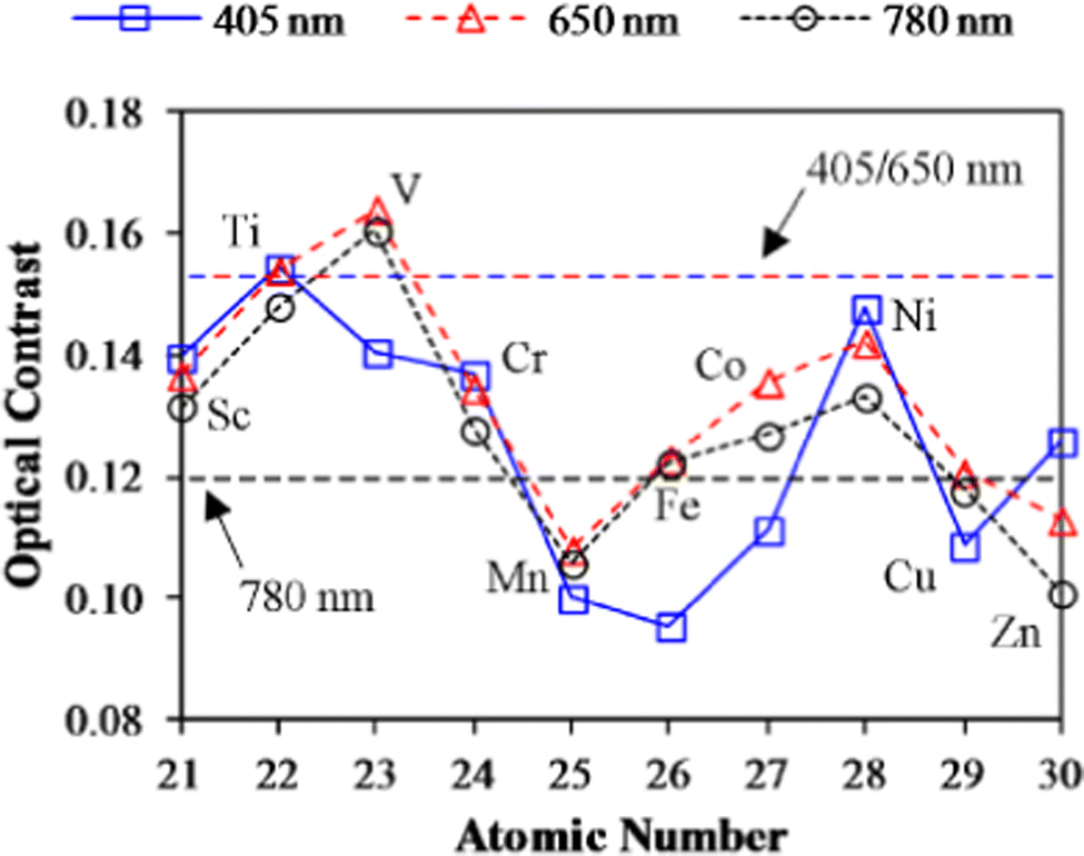 | ||
| Fig. 12 Optical contrast in transition-metal (TM)-doped GST. Adapted with permission from ref. 132. ©2006 IOP. | ||
Ebina et al.74 in 1999 worked on maintaining the stable overwrite cycles for GST, for which they developed a recording layer of O-GST. They opted for oxygen doping in GST due to the high value of Tm for oxides, which was expected to suppress the data flow during overwrite time. The designed optical disk from O-GST was compatible with laser irradiation of 780 nm wavelength.74 The Zn doped GST thin films were also noticed to decrease the optical band gap, which resulted from a decrease in activation energy and hence enhanced the conductivity.50 Another doped GST composition, as studied by Singh et al.,18 reported that Ag doping up to 3% led to an appreciable increase in the optical transmission for the amorphous phase. But after the phase transition, a reduction was reported in transmission due to the presence of resonant p states in the hcp phase.18,91 Vinod et al.58 doped Se into GST and reported a net increase in the optical band gap (Eopt) of Se-GST thin films. The bond energy approach revealed that Ge–Se bonds were more favoured than any other bonds in the structure due to their pronounced electronegativity difference. These Ge–Se bonds have the potential for good glass formation, so doped thin films remained in the amorphous phase up to a particularly high temperature. Also, due to the increased bonding energy of Ge–Se bonds, the overall bond energy of the system got increased and resulted in higher Tc.58 Hence, in a nutshell, Se doping enhanced the electronegativity and cohesive power of GST thin films, which in turn had increased the optical band gap of Se-GST thin films.
Bai et al.60 studied Sn-GST thin films and observed a fast switching behaviour in two stable phases as compared to the undoped one. Regarding optical properties, the authors have reported an improved optical contrast with the addition of the Sn element, as doping altered the texture formation from cylindrical to basal texture in the hcp phase.60,148 However, Kissinger's plot for this doped system depicted that both Tc and crystallization activation energy got reduced with doping of Sn, which caused ultrafast crystallization but at the cost of low thermal stability of the amorphous phase. This reduction in activation energy was due to the emergence of weak Sn–Te bonds having a binding energy of 359.8 kJ mol−1 as compared to that of the binding energy of Ge–Te, i.e., 456 kJ mol−1.148,149 The above discussion on the optical properties upon incorporating various dopants in the GST host is summarized in Table 2.
9 Irradiation effects on Ge2Sb2Te5 thin films
The discussion of several properties of GST emphasizes the role of structure and defects in determining these properties. Most of the methods discussed are equilibrium methods. Also, some non-equilibrium methods exist that can help to stabilize GST and other materials in novel/metastable phases. One such non-equilibrium method is thin film deposition, which is widely used. Another non-equilibrium method is irradiation of materials with low and high-energy ions.153 Low energy ions, with energy in the range of ∼keV, are now routinely used in the semiconductor industry. Such low- and high-energy (∼MeV) ions provide a unique opportunity to synthesize novel materials and modify their properties.When an energetic ion falls on a material, the energy it loses is broadly divided into two categories:153
1. Nuclear energy loss, Sn, and
2. Electronic energy loss, Se.
Here Sn and Se represent the energy losses per unit length for the two cases. Nuclear energy loss is basically the energy lost via collisions (like billiard balls) in which momentum and energy conservation principles are applied. In the electronic energy loss, the energy of the incoming ion is first transferred to the electrons in the materials and then finally to the lattice. In the latter case, the energy transfer mechanism occurs by following the two most used models: the Coulomb explosion model and the thermal spike model.153 The observed changes in GST and other materials using ion beams are due to the introduction of the controlled defects in materials. The number and nature of the defects in materials can be controlled using ion irradiation by controlling various parameters such as energy, ion fluence, ion fluence rate, and ion type.
9.1 Low-energy irradiation
The structure and the properties of GST can be modified using low energy irradiation, where the energy of the incident ions is of the order of a few hundreds of keV. For example, the crystalline nature, stability and crystallization kinetics of GST thin films can be improved by irradiating these thin films with 120 keV Sb+ ions as noted by Bastiani et al.154,155 The crystallization time reduces significantly caused by the collision cascades induced in GST. Rimini et al.156 showed that the fraction of the crystalline phase in GST can be tuned by irradiating the GST films with 120 keV Sb+ ions.156 In addition, these ions can be used to modify the grain distribution in the material. Similar work by Lee et al.157 revealed that this technique could be used to modify the thermal stability and crystallization dynamics in GST thin films using 40 keV Si ions.157 These ions can modify the activation energy and the resistivity of these thin films by controlling the fluence rate of irradiation. Irradiation with 150 keV Ar+ ions can be used to modify the structural and electrical properties of the GST thin films as shown by Privitera et al.158,159 These ions lead to the interesting metal–insulator transitions in these materials by tuning the bonding and the van der Waals gap.9.2 High-energy irradiation
In the MeV range, the effect of swift heavy ions (SHI) on the structural, optical and electrical properties of GST has been studied by Kanda et al.35,55,160 They studied the effect of 120 MeV Ag9+ and 80 MeV Si6+ ions on the structural, optical and electronic properties of pure and Ag-doped GST. They observed crystallization in pure GST films with Ag-ion irradiation. Interestingly, no such crystallization was observed for Ag-doped films. Hence, it will be possible to tune the bandgap and the crystallization kinetics using Ag-ion irradiation.55 The study involving 80 MeV Si-ions35 showed not much effect on the structural properties of pure and Ag-doped GST. A comparison of these results showed that the two energy losses, Se and Sn, play an important role in determining the effects of SHI on the properties of pure and Ag-doped GST. GST was found to be extremely radiation-tolerant, implying its suitability for space and other radiation-rich environments. These studies on the effects of low- and high-energy ions on the properties of pure and doped GST open up new avenues to be explored further in tailoring the properties of GST thin films using novel methods. Further study in this direction is required where a deeper understanding of the effects of the various irradiation parameters on the properties of pure and doped GST, or other chalcogenides, can be investigated. This technique has great potential, is already widely used in the semiconductor industry and can offer unique opportunities.10 Applications of Ge2Sb2Te5 thin films with various dopants
In the past few decades, researchers have successfully revealed the application potential of PCMs in various fields. These materials find their best use in memory devices due to their proficiency in synchronously utilizing the features of non-volatility and low power consumption. Due to the continuous improvement in material fabrication and engineering, PCMs, particularly chalcogenide-based thin films, have become the first choice of researchers for non-volatile memory devices. Recently introduced Intel Optane DC chips based on PCRAM technology already surpass SSD.25 Although, to this date, flash memories are the most successful memory technologies, the ability of PCMs to exhibit rapid and reversible switching between two stable states may lead to their future dominance over existing flash memories.6 Further developments in PCRAM open up new horizons for future applications. Cost-effectiveness and scalability are the two main factors that decide the market sustainability of data storage devices.GST is a widely explored composition for phase change memories due to its superior blended properties, i.e., good thermal stability and fast processing speed. But this stoichiometric composition needs to be tailored to make it ideal as per the demand of the modern data storage industry. One way to tackle this challenge is accomplished by doping the host GST composition. Fig. 13 summarizes the generalized trend followed by various dopants belonging to a specific group from the periodic table to modify the properties of undoped GST thin films. This will further help in choosing a specific dopant as per the specific application requirements. GST's future applications include programmable wires, cognitive computers, neuromorphic photonic computing, etc.6 GST-based PCMs work effectively in mid and far-infrared wavelength regions due to their striking optical contrast between two stable phases, thus making them suitable as sensors and for managing thermal radiation.161 In Fig. 14, some application domains of GST thin films have been highlighted.
 | ||
| Fig. 13 A schematic representation of the periodic table showing a general trend followed by doping elements belonging to a particular class in affecting GST properties. | ||
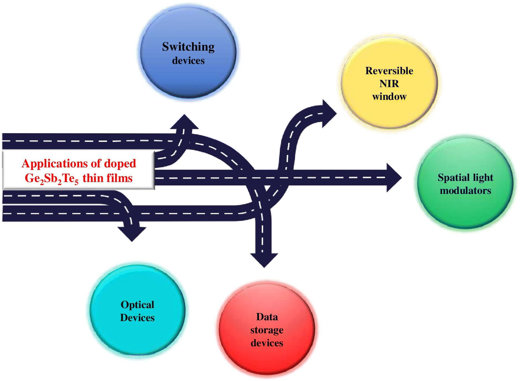 | ||
| Fig. 14 Various applications of doped Ge2Sb2Te5 thin films. | ||
10.1 Applications in optical devices
At present, various compositions of the GeSbTe alloy with different dopants are efficiently meeting the multiple needs of the technological world. Since 1990, this GeSbTe composition has been used mainly as rewritable optical devices. Ge2Sb2Te5 based phase change memory devices are used immensely due to their unique properties compared to the conventional data storage devices.25 They are widely used as optical disks and can be fabricated as per the application requirement due to their tunable electrical and optical properties.162 GST alloy-based thin films are immensely employed in the triple Blu-ray disks because they have all the properties of recording layers even in the nanometer range of thickness. Further, the lamination method (fabricating the material in multiple layers) will increase the probability of recording density.125 Additionally, the addition of dopants into GST enhances and strengthens its properties.163 Here we will discuss some of the applications of the doped GST alloy as reported by various researchers.10.2 Application to switching devices
A high value of RESET current is seen to limit the practical application of GST in switching devices. The researchers reported that doping of GST thin films with elements such as Si, O, N, Ni, W, Zn and As significantly improved their switching performance. Si doping in GST comes with the enhanced feature of recording stability as Si has an ionic radius comparable to that of the host constituent atom Ge, so it resists the atomic diffusivity. These doped thin films were less power-consuming for data writing, which helped to tackle the low-efficiency issue in GST thin films. Similarly, oxygen doping was found to affect the electrical and optical properties of GST thin films in a significant way. As studied by Privitera et al.,66 O-GST thin films led to phase segregation due to oxide formation, which led to an increased Tc and consequent stabilization of the amorphous phase. This enhanced thermal stability of the amorphous phase ultimately strengthened the cyclability of doped GST thin films. On the other hand, Ni doping was perceived to alter the properties of GST thin films by just affecting the electrical properties as it lowered the magnitude of resistance contrast between the amorphous and crystalline phase. Therefore, Ni-GST thin films open up a new window for designing switching devices.10.3 Applications to memory devices
N-GST thin films were found to be suitable for multilevel data storage by stabilizing the fcc phase and suppressing the high-temperature hcp phase. The formation of Ge–N bonds was found to increase the phase transition temperature for fcc to hcp phase transition.166 Similar to N-GST thin films, Ni-GST thin films enhance the thermal stability and hence provide good data retention ability for at least ten years. Cu doping in GST thin films showed a reduced power consumption with an increased data retention ability. As reported by various researchers, Cu-GST thin films exhibit high cyclability due to the lowered Tm value compared to undoped ones. On the other hand, Zn doping improves the performance of PCRAM devices as it hinders the interaction between read and write operations.11 Conclusion
In conclusion, among various existing phase change materials (PCMs), chalcogenide-based compositions lying on the pseudo-binary tie line of GeTe-Sb2Te3 are considered as superior from the application perspective in the modern technological world. These various compositions hold the potential to fulfill different requirements in multiple application domains. But they are widely used in the data storage industry as phase-change random access memory (PCRAM) devices. Notably, the composition Ge2Sb2Te5 (GST) has better qualities than other existing memory devices due to its unique reversible switching between the two stable phases. GST, as compared to its other counterparts, is being considered as the future of ideal data storage devices due to its perfectly blending ability of crystallization speed and thermal stability. Doping of various elements is practiced in the GST host matrix to achieve better thermal stability, fast processing speed, low scalability, high cyclability, good data retention and low power consumption altogether. This review paper highlighted the effect of various dopants on the different properties of GST thin films. In addition to the effect of dopants, a brief discussion on the effect of low- and high-energy irradiation in tailoring various properties of GST films was also covered. The presented article provided an outlook on the future applications of GST in both electrical and optical domains.Conflicts of interest
The authors declare that there is no conflict of interest.Acknowledgements
The authors gratefully acknowledge the support from the Department of Science and Technology, New Delhi, under the Research Project (FILE NO. CRG/2018/001135 dated 22/03/2019). N. B. is thankful to the Department of Science and Technology, New Delhi, for providing financial support as SRF under the above mentioned research project.Notes and references
- M. A. Hassan and Q. M. Rizvi, Computer, 2019, 6, 580–583 Search PubMed.
- M. Harvey, M. Langheinrich and G. Ward, Pervasive Mob Comput., 2016, 27, 14–26 CrossRef.
- O. Surinta and R. Chamchong, International Conference on Intelligent Information Processing, 2008, pp. 182–189 Search PubMed.
- C. T. Meadow, Making connections: Communication through the ages, Scarecrow Press, 2002 Search PubMed.
- S. R. Ovshinsky, Phys. Rev. Lett., 1968, 21, 1450 CrossRef.
- S. Raoux, W. Wełnic and D. Ielmini, Chem. Rev., 2010, 110, 240–267 CrossRef CAS.
- Y. Zhang, J. B. Chou, J. Li, H. Li, Q. Du, A. Yadav, S. Zhou, M. Y. Shalaginov, Z. Fang, H. Zhong, C. Roberts, P. Robinson, B. Bohlin, C. Ríos, H. Lin, M. Kang, T. Gu, J. Warner, V. Liberman, K. Richardson and J. Hu, Nat. Commun., 2019, 10, 1–9 CrossRef PubMed.
- M. Stegmaier, C. Ros, H. Bhaskaran, C. D. Wright and W. H. Pernice, Adv. Opt. Mater., 2017, 5, 1600346 CrossRef.
- Q. Zhang, Y. Zhang, J. Li, R. Soref, T. Gu and J. Hu, Opt. Lett., 2018, 43, 94–97 CrossRef CAS PubMed.
- M. Rudé, J. Pello, R. E. Simpson, J. Osmond, G. Roelkens, J. J. van der Tol and V. Pruneri, Appl. Phys. Lett., 2013, 103, 141119 CrossRef.
- T. Moriyama, D. Tanaka, P. Jain, H. Kawashima, M. Kuwahara, X. Wang and H. Tsuda, IEICE Electron. Express, 2014, 11, 20140538 CrossRef.
- K. Kato, M. Kuwahara, H. Kawashima, T. Tsuruoka and H. Tsuda, Appl. Phys. Express, 2017, 10, 072201 CrossRef.
- D. Tanaka, Y. Shoji, M. Kuwahara, X. Wang, K. Kintaka, H. Kawashima, T. Toyosaki, Y. Ikuma and H. Tsuda, Opt. Express, 2012, 20, 10283–10294 CrossRef CAS PubMed.
- P. Xu, J. Zheng, J. K. Doylend and A. Majumdar, ACS Photonics, 2019, 6, 553–557 CrossRef CAS.
- J. Zheng, A. Khanolkar, P. Xu, S. Colburn, S. Deshmukh, J. Myers, J. Frantz, E. Pop, J. Hendrickson, J. Doylend, N. Boechler and A. Majumdar, Opt. Mater. Express, 2018, 8, 1551–1561 CrossRef CAS.
- S.-Y. Lee, Y.-H. Kim, S.-M. Cho, G. H. Kim, T.-Y. Kim, H. Ryu, H. N. Kim, H. B. Kang, C.-Y. Hwang and C.-S. Hwang, Sci. Rep., 2017, 7, 1–8 CrossRef.
- G. G. Han, H. Li and J. C. Grossman, Nat. Commun., 2017, 8, 1–10 CrossRef CAS.
- P. Singh, A. Singh, J. Sharma, A. Kumar, M. Mishra, G. Gupta and A. Thakur, Phys. Rev. Appl., 2018, 10, 054070 CrossRef CAS.
- Y. Lu, X. Xiao, J. Fu, C. Huan, S. Qi, Y. Zhan, Y. Zhu and G. Xu, Chem. Eng. J., 2019, 355, 532–539 CrossRef CAS.
- J. Xue, C. Zhu, J. Li, H. Li and Y. Xia, Adv. Funct. Mater., 2018, 28, 1705563 CrossRef PubMed.
- T. Wei, J. Wei, K. Zhang, H. Zhao and L. Zhang, Sci. Rep., 2017, 7, 42712 CrossRef CAS.
- P. Hosseini, C. D. Wright and H. Bhaskaran, Nature, 2014, 511, 206–211 CrossRef CAS.
- X.-B. Li, N.-K. Chen, X.-P. Wang and H.-B. Sun, Adv. Funct. Mater., 2018, 28, 1803380 CrossRef.
- M. Wuttig and N. Yamada, Nat. Mater., 2007, 6, 824–832 CrossRef CAS.
- Z. Zhang, Z. Wang, T. Shi, C. Bi, F. Rao, Y. Cai, Q. Liu, H. Wu and P. Zhou, InfoMat, 2020, 2, 261–290 CrossRef CAS.
- M. Wuttig, Nat. Mater., 2005, 4, 265–266 CrossRef CAS PubMed.
- M. Luo and M. Wuttig, Adv. Mater., 2004, 16, 439–443 CrossRef CAS.
- H. J. Kim, J.-W. Sohn, N. Hong, C. Williams and W. Humphreys, J. Phys. Photonics, 2021, 3, 024008 CrossRef CAS.
- Y. Chen, C. Rettner, S. Raoux, G. Burr, S. Chen, R. Shelby, M. Salinga, W. Risk, T. Happ, G. McClelland, M. Breitwisch, A. Schrott, J. Philipp, M. Lee, R. Cheek, T. Nirschl, M. Lamorey, C. Chen, E. Joseph, S. Zaidi, B. Yee, H. Lung, R. Bergmann and C. Lam, 2006 International Electron Devices Meeting, 2006, pp. 1–4 Search PubMed.
- W. Y. Cho, B.-H. Cho, B.-G. Choi, H.-R. Oh, S. Kang, K.-S. Kim, K.-H. Kim, D.-E. Kim, C.-K. Kwak, H.-G. Byun, Y. Hwang, S. Ahn, G.-H. Koh, G. Jeong, H. Jeong and K. Kim, IEEE J. Solid-State Circuits, 2005, 40, 293–300 Search PubMed.
- M. H. Lankhorst, B. W. Ketelaars and R. A. Wolters, Nat. Mater., 2005, 4, 347–352 CrossRef CAS.
- A. Pirovano, A. L. Lacaita, A. Benvenuti, F. Pellizzer and R. Bez, IEEE Trans. Electron Devices, 2004, 51, 452–459 CrossRef.
- F. Merget, D. Kim, P. H. Bolivar and H. Kurz, Microsyst. Technol., 2007, 13, 169–172 CrossRef.
- N. Yamada, E. Ohno, K. Nishiuchi, N. Akahira and M. Takao, J. Appl. Phys., 1991, 69, 2849–2856 CrossRef CAS.
- N. Kanda, A. Thakur, F. Singh and A. Singh, Radiat. Eff. Defects Solids, 2021, 176, 896–905 CrossRef CAS.
- T. Ohta, J. Optoelectron. Adv. Mater., 2001, 3, 609–626 CAS.
- N. Yamada, R. Kojima, M. Uno, T. Akiyama, H. Kitaura, K. Narumi and K. Nishiuchi, Optical Data Storage 2001, 2002, 55–63 CAS.
- M. Kuwahara, S. Takehara, Y. Kashihara, K. Watabe, T. Nakano, M. Tanaka, N. Nakamura, H. Ohsawa and H. Satoh, Jpn. J. Appl. Phys., 2003, 42, 1068 CrossRef CAS.
- P. Singh, A. Singh and A. Thakur, J. Mater. Sci.: Mater. Electron., 2019, 30, 3604–3610 CrossRef CAS.
- G. C. Wicker, Electronics and Structures for MEMS, 1999, pp. 2–9 Search PubMed.
- M. L. Lee, K. T. Yong, C. L. Gan, L. H. Ting, S. B. M. Daud and L. Shi, J. Phys. D: Appl. Phys., 2008, 41, 215402 CrossRef.
- P. Guo, J. A. Burrow, G. A. Sevison, H. Kwon, C. Perez, J. R. Hendrickson, E. M. Smith, M. Asheghi, K. E. Goodson, I. Agha and A. M. Sarangan, Appl. Phys. Lett., 2020, 116, 131901 CrossRef CAS.
- S. Guo, Z. Hu, X. Ji, T. Huang, X. Zhang, L. Wu, Z. Song and J. Chu, RSC Adv., 2014, 4, 57218–57222 RSC.
- K. Ding, K. Ren, F. Rao, Z. Song, L. Wu, B. Liu and S. Feng, Mater. Lett., 2014, 125, 143–146 CrossRef CAS.
- Q. Gao and L. Chen, Appl. Phys. A: Mater. Sci. Process., 2019, 125, 564 CrossRef CAS.
- S. Wei, H. Zhu, K. Chen, D. Xu, J. Li, F. Gan, X. Zhang, Y. Xia and G. Li, Appl. Phys. Lett., 2011, 98, 231910 CrossRef.
- J. Park and J. Bae, J. Electron Microsc., 2015, 64, 381–386 CAS.
- K.-N. Chen, C. Cabral Jr and L. Krusin-Elbaum, Microelectron. Eng., 2008, 85, 2346–2349 CrossRef CAS.
- S. Cheng, S. Wei, X. Yi, J. Wang, C. Liu, J. Li and T. Yang, J. Phys. D, 2015, 48, 475108 CrossRef.
- G. Wang, Q. Nie, X. Shen, R. Wang, L. Wu, J. Fu, T. Xu and S. Dai, Appl. Phys. Lett., 2012, 101, 051906 CrossRef.
- Q. Wang, P. M. Konze, G. Liu, B. Liu, X. Chen, Z. Song, R. Dronskowski and M. Zhu, J. Phys. Chem. C, 2019, 123, 30640–30648 CrossRef CAS.
- P. Singh, P. Sharma, V. Sharma and A. Thakur, Semicond. Sci. Technol., 2017, 32, 045015 CrossRef.
- P. Singh, A. Singh, N. Kanda, M. Mishra, G. Gupta and A. Thakur, Appl. Phys. Lett., 2017, 111, 261102 CrossRef.
- X. Ji-Lin, L. Bo, S. Zhi-Tang, F. Song-Lin and C. Bomy, Chin. Phys. Lett., 2005, 22, 934 CrossRef.
- N. Kanda, A. Thakur and A. Singh, AIP Conf. Proc., 2019, 030260 CrossRef.
- Z. Tan, M. Wen, J. Guo, J. Chen, X. Wu and Z. Song, Solid State Electron., 2021, 186, 108176 CrossRef CAS.
- P. Guo, J. A. Burrow, G. A. Sevison, A. Sood, M. Asheghi, J. R. Hendrickson, K. E. Goodson, I. Agha and A. Sarangan, Appl. Phys. Lett., 2018, 113, 171903 CrossRef.
- E. Vinod, K. Ramesh and K. Sangunni, Sci. Rep., 2015, 5, 8050 CrossRef CAS.
- V. E. Madhavan, M. Carignano, A. Kachmar and K. Sangunni, Sci. Rep., 2019, 9, 1–10 CrossRef CAS.
- N. Bai, F. Liu, X. Han, Z. Zhu, F. Liu, X. Lin and N. Sun, Opt. Laser Technol., 2015, 74, 11–15 CrossRef CAS.
- Y. Lai, B. Qiao, J. Feng, Y. Ling, L. Lai, Y. Lin, B. Cai, B. Chen and T. Tang, J. Electron. Mater., 2005, 34, 176–181 CrossRef CAS.
- S. M. Kim, M. J. Shin, D. J. Choi, K. Lee, S. Hong and Y. Park, Thin Solid Films, 2004, 469, 322–326 CrossRef.
- M. S. Kim, J. H. Jun, J. H. Oh, H. J. Kim, J. S. Roh, S. K. Hong and D. J. Choi, Solid State Phenom., 2007, 21–24 CAS.
- K.-H. Kim, J.-C. Park, J.-H. Lee, J.-G. Chung, S. Heo and S.-J. Choi, Jpn. J. Appl. Phys., 2010, 49, 101201 CrossRef.
- D.-H. Shin, M.-J. Song, J.-W. Kim, G.-H. Kim, K. Hong and D.-S. Lim, Jpn. J. Appl. Phys., 2014, 53, 031402 CrossRef CAS.
- S. Privitera, E. Rimini and R. Zonca, Appl. Phys. Lett., 2004, 85, 3044–3046 CrossRef CAS.
- Z. Xu, B. Liu, Y. Chen, Z. Zhang, D. Gao, H. Wang, Z. Song, C. Wang, J. Ren, N. Zhu, Y. Xiang, Y. Zhan and S. Feng, Solid State Electron., 2016, 116, 119–123 CrossRef CAS.
- E. Cho, Y. Youn and S. Han, Appl. Phys. Lett., 2011, 99, 183501 CrossRef.
- T. Li, L. Wu, X. Ji, Y. Zheng, G. Liu, Z. Song, J. Shi, M. Zhu, S. Song and S. Feng, AIP Adv., 2018, 8, 025201 CrossRef.
- X. Zhou, M. Xia, F. Rao, L. Wu, X. Li, Z. Song, S. Feng and H. Sun, ACS Appl. Mater. Interfaces, 2014, 6, 14207–14214 CrossRef CAS.
- S. Privitera, E. Rimini, C. Bongiorno, R. Zonca, A. Pirovano and R. Bez, J. Appl. Phys., 2003, 94, 4409–4413 CrossRef CAS.
- S. Sandhu, S. Kumar and R. Thangaraj, Phase Trans., 2017, 90, 1013–1024 CrossRef CAS.
- G. Wang, X. Shen, Q. Nie, R. Wang, L. Wu, Y. Lv, F. Chen, J. Fu, S. Dai and J. Li, J. Phys. D: Appl. Phys., 2012, 45, 375302 CrossRef.
- A. Ebina, M. Hirasaka and K. Nakatani, J. Vac. Sci. Technol., A, 1999, 17, 3463–3466 CrossRef CAS.
- T. H. Jeong, H. Seo, K. L. Lee, S. M. Choi, S. J. Kim and S. Y. Kim, Jpn. J. Appl. Phys., 2001, 40, 1609 CrossRef CAS.
- K. Wang, C. Steimer, D. Wamwangi, S. Ziegler and M. Wuttig, Appl. Phys. A: Mater. Sci. Process., 2005, 80, 1611–1616 CrossRef CAS.
- H. Shin, Y.-S. Kang, A. Benayad, K.-H. Kim, Y. Lee, M.-C. Jung, T.-Y. Lee, D.-S. Suh, K. H. Kim, C. Kim and Y. Khang, Appl. Phys. Lett., 2008, 93, 021905 CrossRef.
- G. Singh, A. Kaura, M. Mukul, J. Singh and S. Tripathi, Appl. Phys. A: Mater. Sci. Process., 2014, 117, 1307–1314 CrossRef CAS.
- N. Bala and A. Thakur, J. Mater. Sci.: Mater. Electron., 2022, 1–7 Search PubMed.
- K.-J. Choi, S.-M. Yoon, N.-Y. Lee, S.-Y. Lee, Y.-S. Park, B.-G. Yu and S.-O. Ryu, Thin Solid Films, 2008, 516, 8810–8812 CrossRef CAS.
- S. Ryu, S. Yoon, K. Choi, N. Lee, Y. Park, S. Lee, B. Yu, J. Park and W. Shin, J. Electrochem. Soc., 2006, 153, G234 CrossRef CAS.
- P. K. Khulbe, E. M. Wright and M. Mansuripur, J. Appl. Phys., 2000, 88, 3926–3933 CrossRef CAS.
- T. Matsushita, A. Suzuki, T. Kamitani and M. Okuda, Optical Storage (ISOS'92), 1993, pp. 70–75 Search PubMed.
- N. Yamada and T. Matsunaga, J. Appl. Phys., 2000, 88, 7020–7028 CrossRef CAS.
- Q. Bao-Wei, F. Jie, L. Yun-Feng, L. Yun, L. Yin-Yin, T. Ting-Ao, C. Bing-Chu and C. Bomy, Chin. Phys. Lett., 2006, 23, 172 CrossRef.
- Y. Ling, Y. Lin, B. Qiao, Y. Lai, J. Feng, T. Tang, B. Cai and B. Chen, Jpn. J. Appl. Phys., 2006, 45, L349 CrossRef CAS.
- F. Yang, X. Tang, T. Chen, M. Wang, L. Zhang, J. Han, L. Wan, D. Ke and Y. Dai, Comput. Mater. Sci., 2019, 168, 253–259 CrossRef CAS.
- B. Qiao, J. Feng, Y. Lai, Y. Ling, Y. Lin, B. Cai, B. Chen and T. Tang, Appl. Surf. Sci., 2006, 252, 8404–8409 CrossRef CAS.
- J. Feng, Y. Zhang, B. Qiao, Y. Lai, Y. Lin, B. Cai, T. Tang and B. Chen, Appl. Phys. A: Mater. Sci. Process., 2007, 87, 57–62 CrossRef CAS.
- S.-M. Jeong, K.-H. Kim, S.-M. Choi and H.-L. Lee, Jpn. J. Appl. Phys., 2009, 48, 045503 CrossRef.
- K. Shportko, S. Kremers, M. Woda, D. Lencer, J. Robertson and M. Wuttig, Nat. Mater., 2008, 7, 653–658 CrossRef CAS PubMed.
- N. Yamada, E. Ohno, N. Akahira, K. Nishiuchi, K. Nagata and M. Takao, Jpn. J. Appl. Phys., 1987, 26, 61 CrossRef.
- Z. Sun, J. Zhou and R. Ahuja, Phys. Rev. Lett., 2006, 96, 055507 CrossRef PubMed.
- A. V. Kolobov, P. Fons, A. I. Frenkel, A. L. Ankudinov, J. Tominaga and T. Uruga, Nat. Mater., 2004, 3, 703–708 CrossRef CAS.
- B.-S. Lee, J. R. Abelson, S. G. Bishop, D.-H. Kang, B.-K. Cheong and K.-B. Kim, J. Appl. Phys., 2005, 97, 093509 CrossRef.
- M. Lankhorst, J. Non-Cryst. Solids, 2002, 297, 210–219 CrossRef CAS.
- S. Raoux, Annu. Rev. Mater. Sci., 2009, 39, 25–48 CrossRef CAS.
- N. K. Abrikosov and G. Danilova-Dobryakova, Izv. Akad. Auk. SSSR Neorg. Mater, 1965, 1, 204 CAS.
- S. A. Song, W. Zhang, H. S. Jeong, J.-G. Kim and Y.-J. Kim, Ultramicroscopy, 2008, 108, 1408–1419 CrossRef CAS PubMed.
- T. Matsunaga, N. Yamada and Y. Kubota, Acta Crystallogr., Sect. B: Struct. Sci., 2004, 60, 685–691 CrossRef PubMed.
- M. Xu, Y. Cheng, H. Sheng and E. Ma, Phys. Rev. Lett., 2009, 103, 195502 CrossRef CAS.
- B. Zhang, W. Zhang, Z. Shen, Y. Chen, J. Li, S. Zhang, Z. Zhang, M. Wuttig, R. Mazzarello, E. Ma and X. Han, Appl. Phys. Lett., 2016, 108, 191902 CrossRef.
- P. Guo, A. M. Sarangan and I. Agha, Appl. Sci., 2019, 9, 530 CrossRef CAS.
- K. Singh, S. Kumari, H. Singh, N. Bala, P. Singh, A. Kumar and A. Thakur, Appl. Nanosci., 2021, 1–16 Search PubMed.
- W. Zhang, M. Wuttig and R. Mazzarello, Sci. Rep., 2015, 5, 1–10 Search PubMed.
- Z. Xu, C. Chen, Z. Wang, K. Wu, H. Chong and H. Ye, RSC Adv., 2018, 8, 21040–21046 RSC.
- R. Lan, R. Endo, M. Kuwahara, Y. Kobayashi and M. Susa, J. Electron. Mater., 2018, 47, 3184–3188 CrossRef CAS.
- T. Kato and K. Tanaka, Jpn. J. Appl. Phys., 2005, 44, 7340 CrossRef CAS.
- I.-D. Simandan, F. Sava, A.-T. Buruiana, A.-C. Galca, N. Becherescu, I. Burducea, C. Mihai and A. Velea, Materials, 2021, 14, 3663 CrossRef CAS PubMed.
- M. Li, M. Xie, H. Ji, J. Zhou, K. Jiang, L. Shang, Y. Li, Z. Hu and J. Chu, Appl. Phys. Lett., 2020, 116, 162102 CrossRef CAS.
- J.-P. Gaspard, A. Pellegatti, F. Marinelli and C. Bichara, Philos. Mag. Lett., 1998, 77, 727–744 CAS.
- P. Fons, A. V. Kolobov, M. Krbal, J. Tominaga, K. Andrikopoulos, S. Yannopoulos, G. Voyiatzis and T. Uruga, Phys. Rev. B: Condens. Matter Mater. Phys., 2010, 82, 155209 CrossRef.
- S. Kasap and P. Capper, Springer handbook of electronic and photonic materials, Springer, 2017 Search PubMed.
- I. Petrov, R. Imamov and Z. Pinsker, Sov. Phys. Crystallogr., 1968, 13, 339–342 Search PubMed.
- J. L. Da Silva, A. Walsh and H. Lee, Phys. Rev. B: Condens. Matter Mater. Phys., 2008, 78, 224111 CrossRef.
- N. Yamada, MRS Bull., 1996, 21, 48–50 CrossRef CAS.
- G. D'Arrigo, A. Mio, G. Favaro, M. Calabretta, A. Sitta, A. Sciuto, M. Russo, M. Cal, M. Oliveri and E. Rimini, Surf. Coat. Technol., 2018, 355, 227–233 CrossRef.
- M. Frumar, T. Kohoutek, J. Prikryl, J. Orava and T. Wagner, Phys. Status Solidi B, 2009, 246, 1871–1874 CrossRef CAS.
- M. Naito, M. Ishimaru, Y. Hirotsu and M. Takashima, J. Appl. Phys., 2004, 95, 8130–8135 CrossRef CAS.
- M. Naito, M. Ishimaru, Y. Hirotsu, R. Kojima and N. Yamada, J. Appl. Phys., 2010, 107, 103507 CrossRef.
- B. Hyot, X. Biquard and L. Poupinet, Proceedings of EPCOS, Lugano, Switzerland, 2003 Search PubMed.
- P. Jóvári, I. Kaban, J. Steiner, B. Beuneu, A. Schöps and A. Webb, J. Phys.: Condens. Matter, 2007, 19, 335212 CrossRef PubMed.
- S. Caravati, M. Bernasconi, T. Kühne, M. Krack and M. Parrinello, J. Condens. Matter Phys., 2009, 21, 255501 CrossRef CAS PubMed.
- J. Wang, L. Wang and J. Liu, IEEE Access, 2020, 8, 121211 Search PubMed.
- N. Yamada, Phys. Status Solidi B, 2012, 249, 1837–1842 CrossRef CAS.
- Y. Zheng, M. Xia, Y. Cheng, F. Rao, K. Ding, W. Liu, Y. Jia, Z. Song and S. Feng, Nano Res., 2016, 9, 3453–3462 CrossRef CAS.
- F. Rao, Z. Song, Y. Cheng, X. Liu, M. Xia, W. Li, K. Ding, X. Feng, M. Zhu and S. Feng, Nat. Commun., 2015, 6, 1–6 Search PubMed.
- Y. Jiang, Y. Wang, J. Sagendorf, D. West, X. Kou, X. Wei, L. He, K. L. Wang, S. Zhang and Z. Zhang, Nano Lett., 2013, 13, 2851–2856 CrossRef CAS PubMed.
- T. Matsunaga and N. Yamada, Phys. Rev. B: Condens. Matter Mater. Phys., 2004, 69, 104111 CrossRef.
- B. Kooi, W. Groot and J. T. M. De Hosson, J. Appl. Phys., 2004, 95, 924–932 CrossRef CAS.
- S. Kohara, K. Kato, S. Kimura, H. Tanaka, T. Usuki, K. Suzuya, H. Tanaka, Y. Moritomo, T. Matsunaga, N. Yamada, Y. Tanaka, H. Suematsu and M. Takataa, Appl. Phys. Lett., 2006, 89, 201910 CrossRef.
- J. Skelton and S. Elliott, J. Condens. Matter Phys., 2013, 25, 205801 CrossRef CAS.
- M. A. Luong, N. Cherkashin, B. Pecassou, C. Sabbione, F. Mazen and A. Claverie, Nanomaterials, 2021, 11, 1729 CrossRef CAS PubMed.
- B. Liu, T. Zhang, J. Xia, Z. Song, S. Feng and B. Chen, Semicond. Sci. Technol., 2004, 19, L61 CrossRef CAS.
- J. Kim, J. Park and D.-H. Ko, J. Mater. Sci.: Mater. Electron., 2019, 30, 20751–20757 CrossRef CAS.
- R. Golovchak, Y. Choi, S. Kozyukhin, Y. Chigirinsky, A. Kovalskiy, P. Xiong-Skiba, J. Trimble, R. Pafchek and H. Jain, Appl. Surf. Sci., 2015, 332, 533–541 CrossRef CAS.
- L. Men, J. Tominaga, H. Fuji, T. Kikukawa and N. Atoda, Jpn. J. Appl. Phys., 2001, 40, 1629 CrossRef CAS.
- Y. Hu, R. Zhang, T. Lai, X. Zhu, H. Zou and Z. Song, ECS J. Solid State Sci. Technol., 2017, 6, P866 CrossRef CAS.
- M. Frumar and T. Wagner, Curr. Opin. Solid State Mater. Sci., 2003, 7, 117–126 CrossRef CAS.
- L. Cao, X. Ji, W. Zhu, Q. She, Y. Chen, Z. Hu, S. Guo, Z. Song, F. Rao, B. Qian and L. Wu, ECS Solid State Lett., 2015, 4, P102 CrossRef CAS.
- Y. Zhu, Z. Zhang, S. Song, H. Xie, Z. Song, X. Li, L. Shen, L. Li, L. Wu and B. Liu, Mater. Res. Bull., 2015, 64, 333–336 CrossRef CAS.
- S. Raoux, C. T. Rettner, J. L. Jordan-Sweet, A. J. Kellock, T. Topuria, P. M. Rice and D. C. Miller, J. Appl. Phys., 2007, 102, 094305 CrossRef.
- H.-Y. Cheng, S. Raoux and Y.-C. Chen, J. Appl. Phys., 2010, 107, 074308 CrossRef.
- J. K. Behera, X. Zhou, A. Ranjan and R. E. Simpson, ACS Appl. Mater. Interfaces, 2018, 10, 15040–15050 CrossRef CAS PubMed.
- K. Tanaka, Phys. Status Solidi B, 2020, 257, 1900756 CrossRef CAS.
- K.-H. Song, S.-W. Kim, J.-H. Seo and H.-Y. Lee, J. Appl. Phys., 2008, 104, 103516 CrossRef.
- B. J. Kooi and M. Wuttig, Adv. Mater., 2020, 32, 1908302 CrossRef CAS PubMed.
- Q. Yin and L. Chen, J. Alloys Compd., 2019, 770, 692–700 CrossRef CAS.
- K. Wang, D. Wamwangi, S. Ziegler, C. Steimer and M. Wuttig, J. Appl. Phys., 2004, 96, 5557–5562 CrossRef CAS.
- P. I. Lazarenko, A. A. Sherchenkov, S. S. Kozyukhin, M. Y. Shtern, S. P. Timoshenkov, D. G. Gromov and E. N. Redichev, International Conference on Micro-and Nano-Electronics 2014, 2014, p. 944006.
- N. Kraft, G. Wang, H. Bryja, A. Prager, J. Griebel and A. Lotnyk, Mater. Des., 2021, 199, 109392 CrossRef CAS.
- P. Singh, R. Kaur, P. Sharma, V. Sharma, M. Mishra, G. Gupta and A. Thakur, J. Mater. Sci.: Mater. Electron., 2017, 28, 11300–11305 CrossRef CAS.
- D. K. Avasthi and G. K. Mehta, Swift Heavy Ions for Materials Engineering and Nanostructuring, Springer, 2011 Search PubMed.
- R. De Bastiani, A. Piro, I. Crupi, M. Grimaldi and E. Rimini, Nucl. Instrum. Methods Phys. Res., Sect. B, 2008, 266, 2511–2514 CrossRef CAS.
- R. De Bastiani, A. M. Piro, M. G. Grimaldi, E. Rimini, G. A. Baratta and G. Strazzulla, Appl. Phys. Lett., 2008, 92, 241925 CrossRef.
- E. Rimini, R. De Bastiani, E. Carria, M. G. Grimaldi, G. Nicotra, C. Bongiorno and C. Spinella, J. Appl. Phys., 2009, 105, 123502 CrossRef.
- P.-H. Lee, P.-C. Chang, D.-S. Chao, J.-H. Liang, S.-C. Chang, M.-J. Tsai and T.-S. Chin, Thin Solid Films, 2012, 520, 6636–6641 CrossRef CAS.
- S. M. S. Privitera, A. M. Mio, M. Dück, C. Persch, M. Zimbone, M. Wuttig and E. Rimini, J. Phys. D: Appl. Phys., 2018, 51, 495103 CrossRef.
- S. M. S. Privitera, A. M. Mio, E. Smecca, A. Alberti, W. Zhang, R. Mazzarello, J. Benke, C. Persch, F. La Via and E. Rimini, Phys. Rev. B: Condens. Matter Mater. Phys., 2016, 94, 094103 CrossRef.
- N. Kanda, A. Thakur, F. Singh and A. Singh, Nucl. Instrum. Methods Phys. Res., Sect. B, 2020, 467, 40–43 CrossRef CAS.
- F. Ding, Y. Yang and S. I. Bozhevolnyi, Adv. Opt. Mater., 2019, 7, 1801709 CrossRef.
- J. Tian, H. Luo, Y. Yang, F. Ding, Y. Qu, D. Zhao, M. Qiu and S. I. Bozhevolnyi, Nat. Commun., 2019, 10, 1–9 CrossRef PubMed.
- J. H. Han, K.-S. Jeong, M. Ahn, D.-H. Lim, W. J. Yang, S. J. Park and M.-H. Cho, J. Mater. Chem. C, 2017, 5, 3973–3982 RSC.
- P. Singh and A. Thakur, AIP Conf. Proc., 2018, 100086 CrossRef.
- D. Casasent, Proc. IEEE, 1977, 65, 143–157 CAS.
- X. Yu, Y. Zhao, C. Li, C. Hu, L. Ma, S. Fan, Y. Zhao, N. Min, S. Tao and Y. Wang, Scr. Mater., 2017, 141, 120–124 CrossRef.
| This journal is © The Royal Society of Chemistry 2023 |