
 Open Access Article
 This Open Access Article is licensed under a Creative Commons Attribution-Non Commercial 3.0 Unported Licence
Effect of charge selective contacts on the quasi Fermi level splitting of CuGa3Se5 thin film photocathodes for hydrogen evolution and methylviologen reduction†
Ye
Cheng
a,
Chengcan
Xiao
a,
Behzad
Mahmoudi
b,
Roland
Scheer
c,
A. Wouter
Maijenburg
 b and
Frank E.
Osterloh
*a
b and
Frank E.
Osterloh
*a
aDepartment of Chemistry, University of California, Davis, CA 95616, USA. E-mail: fosterloh@ucdavis.edu
bCenter for Innovation Competence (ZIK) “SiLi-nano”, Martin Luther University Halle-Wittenberg, Karl-Freiherr-von-Fritsch-Str. 3, D-06120, Halle (Saale), Germany
cInstitute of Physics, Martin Luther University Halle-Wittenberg, Von-Danckelmann-Platz 3, D-06120, Halle (Saale), Germany
First published on 22nd November 2022
Abstract
The copper chalcopyrite CuGaSe2 and the defect-related phase CuGa3Se5 are promising photocathode materials for solar hydrogen generation. Existing devices exhibit photocurrents nearing 68% (CuGa3Se5)–86% (CuGaSe2) of their theoretical limit but they are plagued by photovoltage losses that reduce their energy conversion efficiency. To evaluate the reasons, we determine the light intensity dependent quasi-Fermi level splitting (QFLS) in p-CuGa3Se5/liquid junctions for the first time, using the vibrating Kelvin probe surface photovoltage technique. The QFLS, or internal photovoltage, corresponds to the maximum electrochemical work a photoelectrode can perform under a given illumination condition. In the presence of water or methylviologen (2+/+) as electron acceptors, the QFLS of Mo/p-CuGa3Se5/liquid junctions reaches 0.22 to 0.29 V, respectively, under 49 mW cm−2 400 nm illumination, while the QFLS of a FTO/p-CuGa3Se5 photoelectrode is only 0.15–0.16 V. The lower voltage of the latter is attributed to a Schottky junction at the back contact, which limits majority charge carrier (hole) extraction from the semiconductor. Photovoltage losses also result from Fermi level pinning of the minority carriers at surface states 0.5 eV above the CGSe valence band. This problem can be overcome by chemical bath deposition of a CdS overlayer, which functions as a selective contact for electron extraction from CuGa3Se5 and which raises the QFLS to 0.44 V at 49 mW cm−2. No significant QFLS enhancement occurs upon adsorption of Cd2+ ions to the CuGa3Se5 electrode surface, suggesting that Cd2+ adsorption alone does not remove the Fermi level pinning effect. Overall, these results provide a better understanding of the effect of surface treatments and charge selective contacts on the photovoltage of CuGa3Se5 photoelectrodes and indicate pathways to improve its solar fuel conversion efficiency.
Broader contextThe photoelectrochemical water splitting reaction is a promising pathway to hydrogen fuel from solar energy. The copper chalcopyrites function as photocathodes for solar hydrogen generation but are plagued by photovoltage losses that reduce their energy conversion efficiency. To evaluate the reasons, we determine the light intensity dependent quasi-Fermi level splitting (QFLS) in p-CuGa3Se5/liquid junctions for the first time, using the Vibrating Kelvin Probe Surface Photovoltage Spectroscopy (VK-SPS) technique. The QFLS, or internal photovoltage, corresponds to the maximum electrochemical work a photoelectrode can perform under a given illumination condition. It cannot be observed with standard photoelectrochemical measurements but is accessible with VK-SPS. We find that on the photoelectrode front side, the internal photovoltage is limited by Fermi level pinning of the minority carriers at surface states 0.5 eV above the p-CuGa3Se5 valence band. Higher photovoltages are obtained after bath deposition of a CdS overlayer which functions as a selective contact for electron extraction from CuGa3Se5. On the back side photovoltage losses result from a Schottky junction between FTO and p-CuGa3Se5, which traps photoholes at the interface. The photovoltage can be raised by replacing the FTO with a molybdenum substrate, which has a lower barrier for hole transfer. These observations provide a better understanding of the effect of surface treatments and charge selective contacts on the solar fuel conversion efficiency of CuGa3Se5 photoelectrodes. |
Introduction
Due to their tunable band gaps (1.0–1.85 eV), high absorption coefficients and usability in the polycrystalline state, copper chalcopyrites, Cu(InxGa1−x)Se2 (CIGS) (x = 0,…,1), are established light absorbers in thin film photovoltaic (PV) applications.1–3 Recently, these materials have also been applied as photocathodes for photoelectrochemical proton reduction (Fig. 1).4–15 For this use, the copper-poor phase CuGa3Se5 (CGSe) has emerged as a champion.13,14 Its structure is obtained from the zinc blende (ZnS) crystal structure by replacing Zn atoms with equal amounts of Cu and Ga (Fig. 1a) and by then removing one formula unit of Cu2Se. This increases the band gap to 1.86 eV, which provides a larger driving force for proton reduction,11 allowing photocurrents of 68% of the theoretical limit (−12.1 mA cm−2 measured at −0.40 V vs. RHE).14 However, the photovoltage of CuGa3Se5 photocathodes (0.2 V, which corresponds to only 11% of the band gap) continues to be very low13,14 The Sivula group reported that photovoltage losses in the related CuIn0.3Ga0.7S2 photocathode are caused by surface Ga and In vacancies.16 Similar surface defects may limit the operation of the CuGa3Se5 (CGSe) photocathode. Indeed, it has been shown that surface treatment with CdS boosts proton reduction with copper and silver chalcopyrites.5,10,11,15,17–19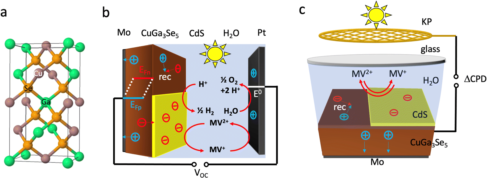 | ||
| Fig. 1 (a) Crystal structure of CuGaSe2, the parent phase of CuGa3Se5, (b) PEC cell, (c) liquid SPV configuration. MV = methylviologen. | ||
To better understand the performance of CuGa3Se5, we have analyzed the photochemical charge separation properties of several CGSe/liquid junctions with vibrating Kelvin probe liquid surface photovoltage spectroscopy (VK-SPV). In this technique, the contact potential difference (CPD) of the sample is measured with a commercially available vibrating Kelvin probe (Besocke Delta Phi). Illumination disturbs the distribution of the charge carriers in the sample and changes the CPD, producing a surface photovoltage (SPV), as shown in eqn (1) and Fig. 1c. This SPV signal equals the Quasi Fermi Level Splitting (QFLS) energy, according to eqn (2).20–24
| SPV = CPD(light) − CPD(dark) | (1) |
 | (2) |
Once the QFLS is known, eqn (2) can also be used to calculate the minority carrier (electron) potential EF,n from the majority carrier (hole) potential EF,p. The latter is accessible from open circuit potential measurements viaeqn (3).39–41 In this equation, EC is the potential of the counter electrode.
 | (3) |
Results and discussion
CGSe thin film photocathodes were grown by physical vapor deposition as reported before.14 The samples, noted as Mo–CGSe and FTO–CGSe, respectively, consist of 2 μm thick CuGa3Se5 on molybdenum- or FTO-coated soda-lime glass. Photographs, SEM, XRD and optical absorption spectra of the films are shown in Fig. S1 (ESI†).14 Linear sweep voltammetry scans for the two electrodes immersed in a 0.05 M sodium phosphate buffer (with 0.1 M Na2SO4) under 400 nm illumination with an intensity of 81 mW cm−2 are compared in Fig. 2a. Cathodic photocurrents are attributed to the hydrogen evolution reaction (HER), as confirmed by gas bubble formation. The photocurrent reaches −3 mA cm−2 at 0 VRHE for the Mo–CGSe electrode, which is approximately one-third of the photocurrent achieved in a 0.5 M H2SO4 electrolyte under AM 1.5G solar irradiance reported previously by the Maijenburg group.14 This difference is due to the lower proton concentration in the sodium phosphate electrolyte (pH 7) used here, which slows down the hydrogen evolution reaction (HER). The slow HER also causes the capacitive current (sawtooth shape), which represents trapping of photogenerated charge carriers at the CGSe/electrolyte interface.42 Based on the standard water reduction potential and the photocurrent onset potential Eon, the external photovoltage Vph (ext, LSV)43 of the Mo–CGSe/NaPi system is
  similar to the previously reported value.14 In comparison, the FTO–CGSe/NaPi electrode has a lower photocurrent and a later photo-onset, corresponding to a lower external photovoltage
  .
.
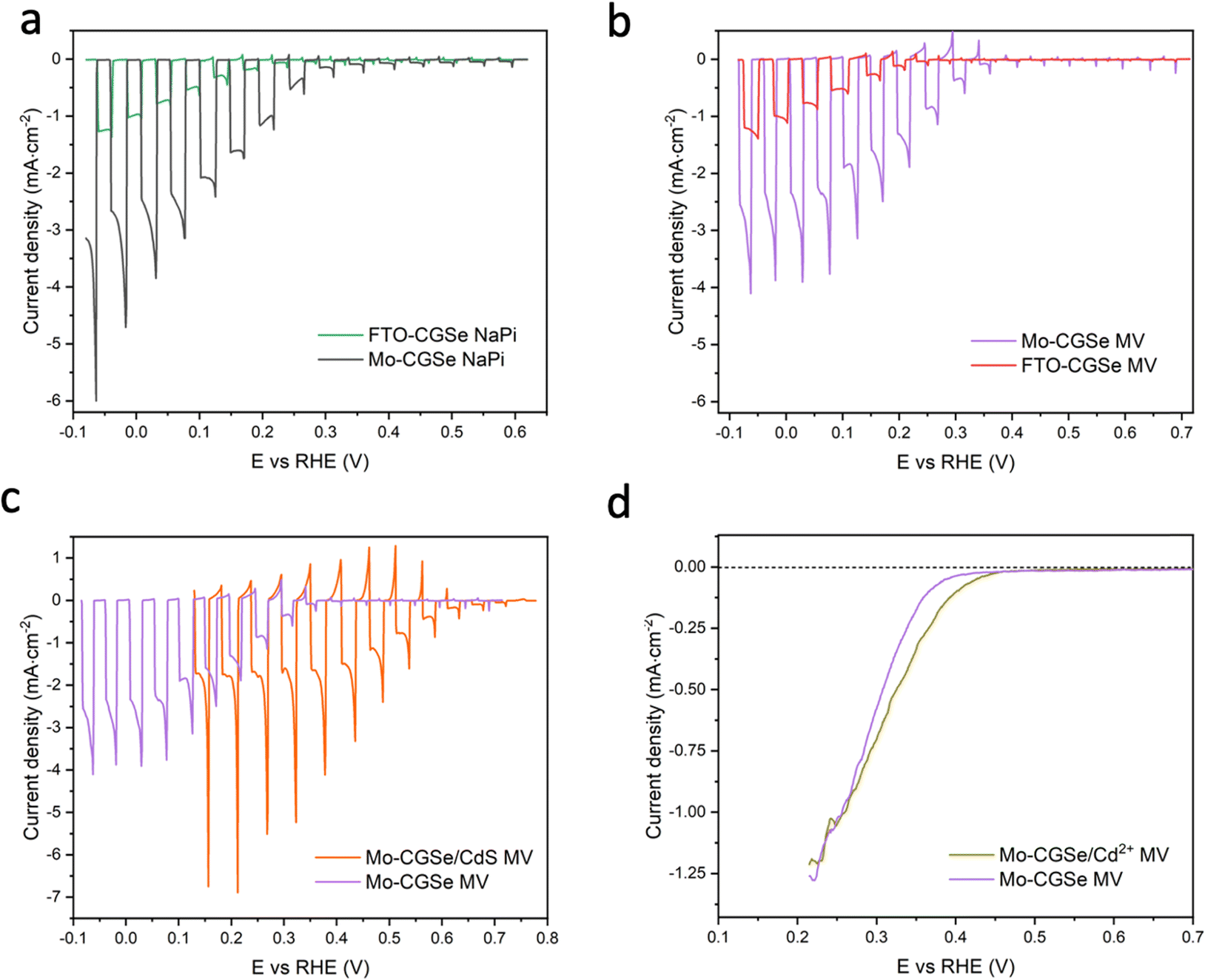 | ||
| Fig. 2 Linear sweep voltammetry (LSV) scans under chopped illumination (400 nm, 81 mW cm−2) for (a) Mo–CGSe and FTO–CGSe in NaPi, (b) Mo–CGSe and FTO–CGSe in MV, (c) Mo–CGSe and Mo–CGSe/CdS in MV, (d) Mo–CGSe and Mo–CGSe/Cd2+ in MV. Continuously illuminated scans are shown here to highlight the difference in photocurrent onset potentials. Chopped scans are shown in Fig. S2 (ESI†). Electrolytes were de-aerated by continuous N2 bubbling. NaPi is 0.1 M Na2SO4/0.05 M sodium phosphate buffer (pH = 7) and MV is 0.01 M MVCl2/0.05 M sodium phosphate buffer (pH = 7). | ||
In order to determine the degree to which the photoelectrode performance is limited by the water reduction overpotential, the electrolyte was replaced with a solution of 0.01 M methylviologen chloride in 0.05 M sodium phosphate buffer. MV2+ is a fast and reversible electron acceptor with E0 = −0.03 VRHE at pH 7.44 As can be seen from Fig. 2b, the photoelectrochemical response of the Mo–CGSe and FTO–CGSe films is nearly unchanged. Photocurrents are −1.0 mA cm−2 and −2.4 mA cm−2 at −0.03 VRHE for the FTO–CGSe and Mo–CGSe electrodes, respectively, and the photovoltage values are 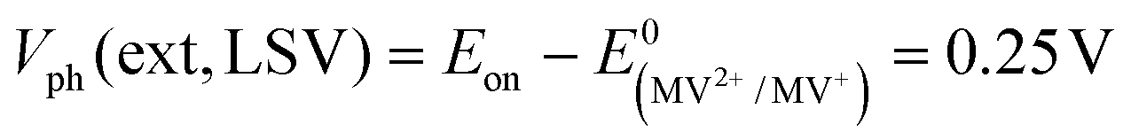 and 0.38 V, respectively. Again, the FTO–CGSe electrode underperforms in comparison to the Mo–CGSe electrode.
The reason for the different performances of both electrodes can be understood with the energy diagrams in Fig. 3a and b. The FTO/CGSe interface contact produces a Schottky junction due to the workfunction difference of the materials. The resulting hole transfer barrier from CGSe to FTO causes trapping of holes at the interface and reduces the quasi-Fermi level splitting and photovoltage of the FTO/CGSe photoelectrode. The Mo/CGSe contact in Fig. 3b is better suited for majority carrier extraction, because the higher work function of Mo reduces the barrier for hole transfer from CGSe to Mo. Additionally, molybdenum is well-known to form low-defect contacts with chalcopyrites due to the formation of a passivating MoSe2 layer at the interface.47–49
 | ||
| Fig. 3 Energy diagrams for (a) FTO–CGSe/NaPi/MV, (b) Mo–CGSe/NaPi/MV, (c) Mo–CGSe/CdS/MV junctions showing band bending and QFLS under illumination at open circuit. The work function of solvent-cleaned FTO is 4.48 to 4.73 eV,45 while the work function of the Mo-substrate (110) is 4.9–5.0 eV.46 Using the EF values for CGSe (0.53–0.60 VRHE) from Fig. S4 (ESI†), the Schottky barrier height of FTO/CGSe is 0.2–0.5 eV and that of Mo/CGSe is ∼0 eV (near ohmic contact). CGSe band edges are based on Mahmoudi et al.14 Standard reduction potentials were taken from ref. 44 and adjusted to RHE, as described in the Experimental section. | ||
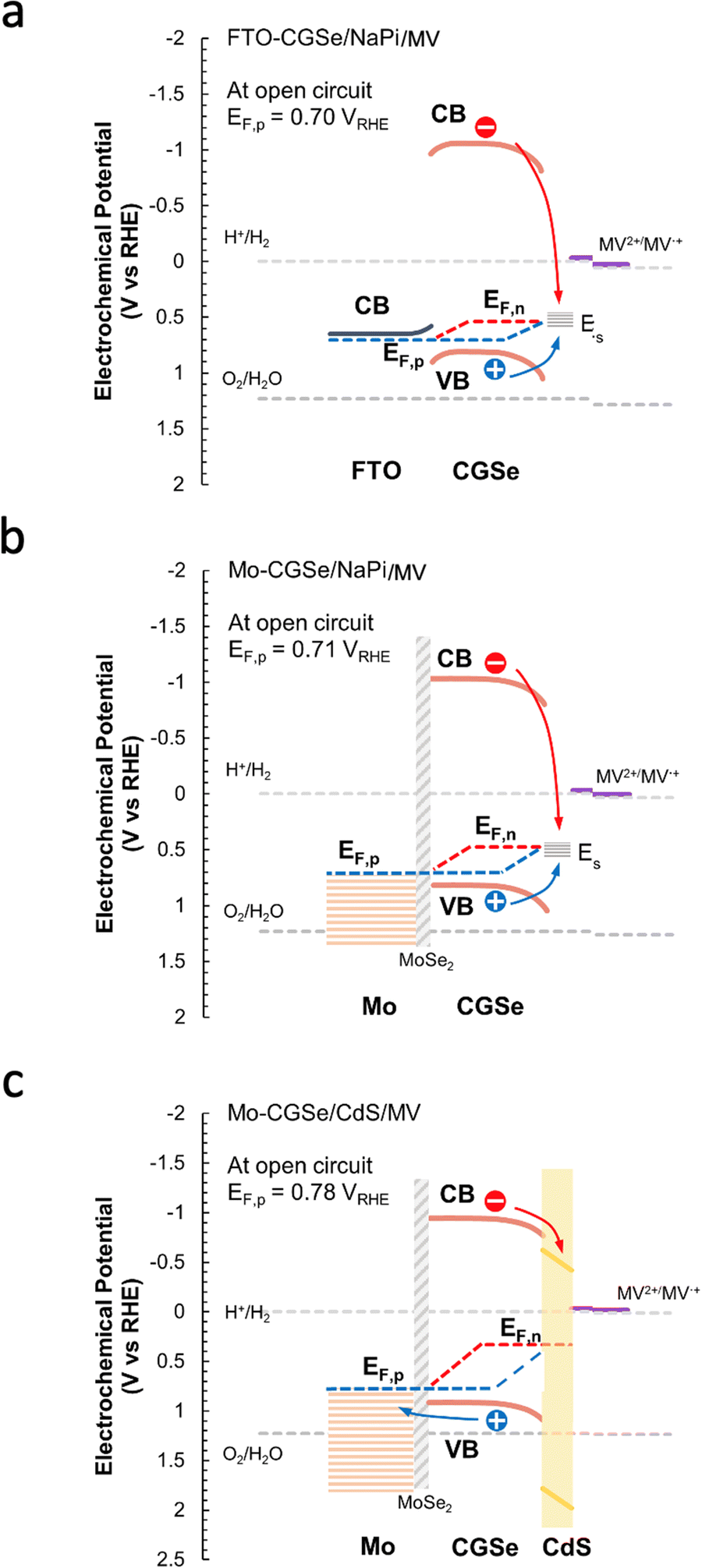
To probe the QFLS of these junctions, surface photovoltage measurements were employed. Full SPV spectra for each photoelectrode in contact with an aqueous 0.01 M methylviologen electrolyte and sodium phosphate buffer (NaPi) are shown in Fig. 4. All samples generate positive photovoltage signals, in agreement with the charge transfer scheme in Fig. 4a. Generally, the photovoltage begins at 1.5 eV, approximately 0.35 eV below the optical band gap (1.85 eV), which is attributed to the excitation of sub-bandgap defects, likely at the CGSe interfaces. A slightly higher signal at 1.3–1.5 eV for FTO–CGSe (shown by a grey square) indicates a higher defect concentration for this sample, possibly due to GaCu and GaSe, and copper vacancies VCu.50,51 The SPV signal above 1.8 eV is due to band gap excitation of CGSe while the double peaks at 2.0 eV and 3.0 eV are a result of the emission characteristics of the Xe light source (Fig. S3, ESI†).
 | ||
| Fig. 4 SPV spectra of the CGSe-electrodes. (a) Charge transfer leading to the SPV signal for a p-type semiconductor-solid–liquid junction. Spectra for the (b) FTO–CGSe/MV, (c) Mo–CGSe/NaPi, and (d) Mo–CGSe/MV; 0.01 M MVCl2 in 0.05 M sodium phosphate buffer (pH = 7). SPV discontinuities at 1.45 and 2.07 eV are due to monochromator filter-changes. SPV onsets are found at 1.5 eV, except for (b) which has a slightly lower onset at 1.3 eV, indicating a sub-band gap defect. | ||
To obtain light intensity dependent QFLS data, SPV measurements were repeated under transient illumination (Fig. 5). A 400 nm LED light source was used to ensure band gap excitation of CuGa3Se5. As before, positive SPV signals arise from the transfer of majority carriers (holes) into the electric contact at the CGSe backside and of minority carriers (electrons) into surface states. Signals are mostly reversible and increase with light intensity, as expected for the QFLS of a junction.27 Baseline drifts indicate trapping of charge carriers at the interfaces. Overall, the Mo–CGSe electrodes produce a larger SPV signal than the FTO–CGSe electrodes, regardless if water (NaPi) or methylviologen is used as the electron acceptor. This confirms the improved charge carrier separation for Mo–CGSe electrodes as already seen in the former PEC measurements (Fig. 2) and as postulated by the energy schemes in Fig. 3.
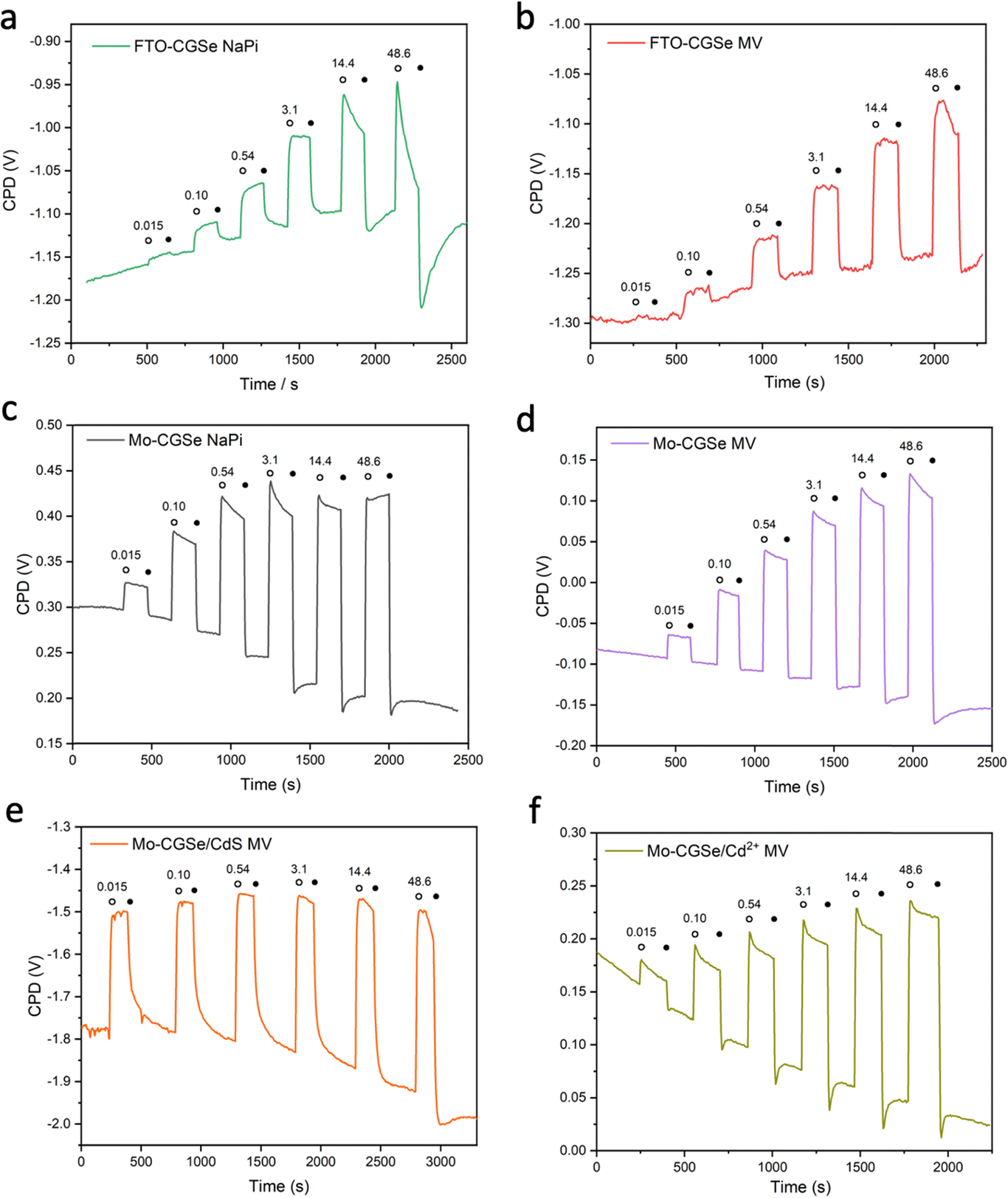 | ||
| Fig. 5 Surface photovoltage (SPV) data as a function of light intensity (mW cm−2) from a 400 nm LED. (a) FTO–CGSe/NaPi, (b) FTO–CGSe/MV, (c) Mo–CGSe/NaPi, (d) Mo–CGSe/MV, (e) Mo–CGSe/CdS/MV, and (f) Mo–CGSe/Cd2+/MV. | ||
Together with the light intensity dependent open circuit potentials (Fig. S4, ESI†), the SPV data was used to construct the QFL plots in Fig. 6. In both MV and NaPi electrolytes, EF,p becomes more oxidizing with increasing light intensity, as expected for a photocathode. On the other hand, EF,n stays constant and remains close to the energy of the surface states (likely gallium vacancies16), approximately 0.5 eV above the valence band edge. This phenomenon is known as Fermi level pinning and has been documented for many semiconductor electrodes,16,43,52–55 incl. chalcopyrites.54
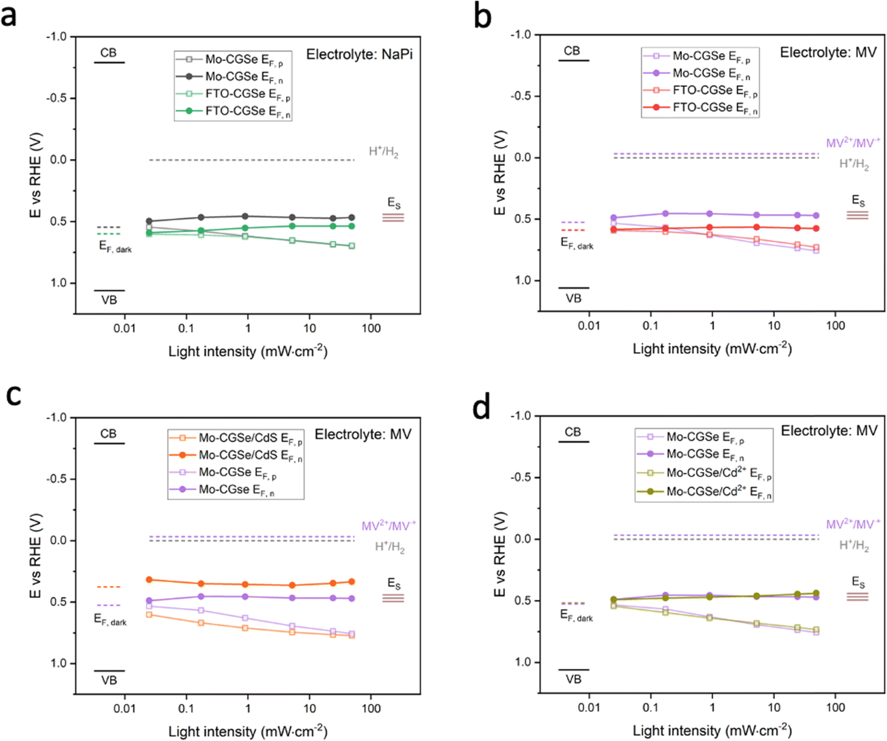 | ||
| Fig. 6 Quasi-Fermi level (QFL) plots versus the logarithm of light intensity (400 nm LED). (a) Mo–CGSe/NaPi versus FTO–CGSe/NaPi. (b) Mo–CGSe/MV versus FTO–CGSe/MV. (c) Mo–CGSe/CdS/MV versus Mo–CGSe/MV. (d) Mo–CGSe/Cd2+/MV versus Mo–CGSe/MV. | ||
Additionally, it can be seen that the FTO–CGSe electrode produces EF,n potentials ∼0.1 V (0.063 V for NaPi and 0.108 V for MV) less reducing than the Mo–CGSe electrode. This is a result of the Schottky junction in Fig. 3a, which promotes electron–hole recombination at the FTO–CGSe interface. Despite the better photovoltage of the Mo–CGSe electrode, EF,n remains too weak to reduce protons nor MV2+ even under the highest illumination intensity. This explains the need for an applied potential that is more negative than 0.3 VRHE to produce a cathodic photocurrent (Fig. 2a and b). As mentioned above, surface modification of Cu-based chalcogenide photocathodes with a thin layer of n-type CdS reduces the photovoltage loss and gives larger cathodic photocurrents.5,15,19,56,57 To test the effect of this treatment on the present system, a thin layer of CdS was deposited on the surface of the Mo–CGSe electrode by the reported chemical bath deposition (CBD) method.15 Photographs, SEM and EDX mapping data of the resulting electrode are shown in Fig. S5 (ESI†). The CdS layer is uniform and retains the sub-micrometer morphology of the underlying Mo–CGSe substrate.
Indeed, the PEC performance of the resulting Mo–CGSe/CdS for MV2+ reduction is enhanced significantly (Fig. 2c). The photo-onset for MV2+ reduction shifts from 0.35 VRHE to 0.65 VRHE, increasing the photovoltage to 0.68 V (from 0.38 V for the bare Mo–CGSe photoelectrode). Also, the photocurrent more than doubles at 0.35 VRHE, but the saturated photocurrent does not exceed −2.5 mA cm−2. This is attributed to the low MVCl2 concentration (0.01 M) in the electrolyte and the slow mass transport resulting from it. Additionally, large (>4 mA cm−2) transient cathodic and smaller anodic (>1 mA cm−2) current spikes indicate a strong capacitive current component that is attributed to electron trapping/de-trapping in the CdS layer of the p–n-CGSe/CdS junction.58–60
The sequence of SPV and OCP measurements was repeated for the Mo–CGSe/CdS–MV junction (Fig. 5 and Fig. S4, ESI†) to produce the QFL data in Fig. 6e. It can be seen that the CdS layer raises the EF,n potentials above the energy ES of the surface states over the entire illumination range and even in the dark (EF). This proves that the CdS layer removes or modifies the Fermi level pinning states at the CGSe electrode surface. Additionally, EF,p levels are found to be 0.02–0.10 V more oxidizing than before, especially at the lower illumination intensity, and that on average the QFLS is increased by 40%. This illustrates the better charge separation at the CGSe–CdS interface, resulting from the introduction of the p-/n-junction, as shown in Fig. 3c. While the junction promotes electron extraction via an electric field, the deep CdS valence band, relative to CGSe, acts as a hole mirror. Overall, the QFL data agree well with the observed increase in the photoelectrochemical MV reduction behavior of the CdS-modified Mo–CGSe electrode.
Lastly, we use the SPV/OCP approach to differentiate the effect of the p-/n-junction from the effect of surface passivation. It is well-known that photovoltage losses at CGSe photocathodes can be reduced by the application of cadmium salts.61–63 For example, surface pretreatment with cadmium ions before the deposition of buffer layers was reported to improve the performance of Cu(In,Ga)Se2-, CuInSxSe2−x- or CuGa3Se5-based solar cells.61,63 This was mainly attributed to the incorporation of Cd2+ at the surface and the removal of the surface oxide. To investigate this possibility, the Mo–CGSe electrode was soaked in a 0.1 M aqueous cadmium acetate solution at 65 °C for 30 min, followed by washing with water. Samples treated this way contain small amounts of Cd2+ on their surface, as confirmed by X-ray photoelectron spectroscopy (XPS) (Fig. S6, ESI†). This compares to observations in the literature.44
The LSV of the resulting electrode in MV electrolyte is shown in Fig. 2d. Compared to the non-treated sample, the LSV curve shows a 0.05 mV anodic shift of the photocurrent onset potential and a small boost in photocurrent, which disappears at more reducing potentials. This shows that the surface treatment with Cd2+ improves the photocathode performance to a small extent, but not nearly as much as a CdS overlayer. Using the data in Fig. 5f and Fig. S4f (ESI†), the QFL plot for the Cd-ion-modified Mo–CGSe electrode was constructed in Fig. 6d. No significant changes occur with the quasi Fermi levels and, importantly, no increase in the QFLS (the internal photovoltage) is seen. This suggests that Cd2+ adsorption alone does not suppress charge carrier recombination at the CGSe surface and does not remove the Fermi level pinning effect. The observed small improvement in the PEC behavior in Fig. 2d must therefore be due to other factors, e.g. a change of the surface charge or of the band edge potentials. However, to improve the internal photovoltage of the electrode, a full CdS layer and a p-/n-junction are needed.
Conclusions
For the first time, surface photovoltage (SPV) measurements were used to measure the quasi-Fermi level splitting (QFLS) in CuGa3Se5 thin film photocathodes in contact with different electrolytes, back contacts, and before and after surface treatments. For the non-treated electrodes, Fermi level pinning near the surface states, 0.5 eV above the CGSe valence band, is confirmed as the cause for the voltage loss during photoelectrochemical water and methyl viologen reduction. The surface states both limit the band bending at the CGSe/liquid interface and they serve as electron–hole recombination centers. Application of a CdS surface layer improves performance, as established by prior works, and increases the internal photovoltage to 0.44 V (MV) under 49 mW cm−2 illumination at open circuit. This increase is due to the electron selective properties of the CGSe/CdS interface (the CdS valence band maximum is too oxidizing to accept holes from CGSe) and the formation of a p-/n-junction. Molybdenum is confirmed to be a better back contact for CGSe than FTO, based on the increased internal photovoltage (from 0.16 V to 0.22 V in NaPi electrolyte under 49 mW cm−2 illumination). This confirms the hypothesis that the photovoltage of FTO/CGSe is limited by the poor hole selectivity of the Schottky junction at the interface. Overall, these findings provide a better understanding of the photoelectrochemistry of CGSe photoelectrodes. Additionally, this work confirms SPV as a powerful method to measure internal photovoltage in semiconductor/liquid junctions and to identify efficient charge-selective contacts.Experimental section
Chemicals
Sodium phosphate monobasic monohydrate (≥99.0%, Sigma-Aldrich), sodium phosphate dibasic heptahydrate (98.0%, Sigma-Aldrich), sodium sulfate (≥99.0%, Sigma-Aldrich) and methyl viologen dichloride hydrate (98%, Acros Organics) were used for the preparation of the electrolytes. Cadmium acetate dihydrate (analytical reagent, Mallinckrodt), thiourea (99%, Alfa Aesar) and ammonium hydroxide (29.7%, certified ACS plus, Fisher Chemicals) were used for the cadmium sulfide chemical bath deposition. Potassium ferricyanide (99.2%, Sigma) and potassium hexacyanoferrate(II) trihydrate (98.0–102.0%, Sigma-Aldrich) were used as received. Water was purified to a resistivity of 18 MΩ cm by a Nanopure system.CuGa3Se5 (CGSe) films were prepared by single-stage co-evaporation of high-purity Cu, Ga and Se onto 2 × 2 cm2 pieces of Mo-coated soda-lime glass containing Na (Guardian Industries Corp.) and FTO-coated soda-lime glass (Sigma-Aldrich). High-vacuum physical vapor deposition was performed simultaneously on FTO and Mo while rotating substrates at 10 rpm to have a homogeneous deposition. The nominal temperature of the substrates was kept at 625 °C. The atomic ratio of (Cu/Ga) was close to 0.33 (0.33 < [Cu/Ga] < 0.37) for all the samples which were analyzed later by energy dispersive X-ray spectroscopy (EDX) using an EDAX Genesis installed on a JEOL SEM-4701F with a cold field emitter using an accelerating voltage of 15 kV.
Cadmium acetate treatment
Inspired by previous works,62,63 the film was soaked in an aqueous 0.1 M cadmium acetate solution at 65 °C for 30 min. The film was then rinsed with water to remove excess reagent.CdS layer deposition
CdS layers were formed on the surface of CGSe films by the chemical bath deposition (CBD) method.15 Prior to CdS deposition, the surface of the CGSe films was pretreated with an aqueous solution containing 2 M NH4OH and 7.5 mM Cd(CH3COO)2 at 80 °C for 10 min. CBD of CdS was performed by immersing the Cd2+-pretreated films in a bath solution containing 0.375 M SC(NH2)2, 7.5 mM Cd(CH3COO)2 and 2 M NH4OH at 65 °C for 5 min. After CdS deposition, the samples were annealed in air at 300 °C for 60 min.Scanning electron microscopy (SEM) and energy dispersive X-ray spectroscopy (EDX) were recorded using a Scios DualBeam FIB/SEM.
X-ray photoelectron spectroscopy (XPS) was conducted using a Supra XPS spectrometer with an Al Kα source that generates X-rays at 1487 eV. All analysis was done in the ultra-high vacuum (UHV) analytical chamber with a pressure of 10−7 mbar. The survey scan was conducted at a constant pass energy of 40 eV with a scan step of 0.5 eV, and the high-resolution core-level spectra were recorded at a constant pass energy of 40 eV with a scan step of 0.1 eV. The spectra were electrostatically corrected based on the position of C 1s (284.8 eV).
Photoelectrochemical (PEC) linear sweep voltammetry (LSV) measurements
Photoelectrochemical measurements were conducted using a Gamry Reference 600 Potentiostat connected to a typical three-electrode system, with a Pt counter electrode and a calomel reference electrode (3.5 M KCl). All the PEC measurements were performed with stirring and continuous N2 purging. LSV scans were performed with a 10 mV s−1 scan rate in the cathodic direction. The potentials in each measurement were converted to the normal hydrogen electrode (NHE) by calibration in 10 mM K3Fe(CN)6/K4Fe(CN)6. Potentials were adjusted to RHE with the following formula: VRHE = VNHE + 0.0592 × pH. The same 400 nm LED described for the SPV measurements below was used as the light source.The electrolytes used were as follows: NaPi: 0.1 M Na2SO4 with 0.05 M sodium phosphate buffer (pH = 7); MV: 0.01 MVCl2 with 0.05 M sodium phosphate buffer (pH = 7). The pH of the electrolytes was measured with a pH meter (Fisher Scientific accumet AE150).
Open circuit potential (OCP) measurements
A two-electrode setup was used for the OCP measurements by using a calomel electrode (3.5 M KCl) as the counter/reference electrode and the CGSe electrode as the working electrode. All OCP measurements were performed with stirring and continuous N2 purging. The potentials in each measurement were converted into the values versus RHE as described above. The same 400 nm LED light source was used.Surface photovoltage (SPV) measurements
Contact potential differences (CPD) were measured using a circular (2.5 mm diameter), semitransparent vibrating gold mesh disk (Kelvin Probe S, Besocke Delta Phi) that was mounted inside of a home-built vacuum chamber and controlled by a Kelvin Control 7 Oscillator/amplifier (Besocke Delta Phi). Samples were placed approximately 1 mm underneath the Kelvin probe. A 150 W Xe lamp passing through an Oriel Cornerstone 130 monochromator was used as the light source for the full SPV spectra. For transient SPV data, a 400 nm LED (LZC-00UA00, LedEngin) was used as the light source, and the irradiation power was controlled by a power supply (Naweisz NP6005). Light intensity was measured with a photometer (International Light IL1400BL) equipped with a SEL005 detector. SPV data was recorded every 5 seconds by measuring the contact potential difference (CPD) value at each step. For liquid SPV measurements, 15 μL of the respective liquid electrolyte was dropped on the surface of the sample and then covered with a microscope cover glass (Fisher Scientific, thickness 0.17–0.25 mm). During the measurements, the chamber was continuously purged with a water-saturated N2 flow (flow rate of 0.02–0.10 SLPM, standard liter per minute) to suppress the evaporation of the electrolyte.Author contributions
The experiments were designed by F. E. O. and conducted by Y. C. and C. X. CuGa3Se5 films were prepared by B. M. and A. W. M. with assistance by R. S. The manuscript was written by F. E. O. and Y. C. with additional contributions by all other authors. All authors have given approval to the final version of the manuscript.Conflicts of interest
There are no conflicts to declare.Acknowledgements
The authors thank the U.S. Department of Energy, Office of Science, Office of Basic Energy Sciences under Award Number DOE-SC0015329 for financial support of this work. The Kratos Supra XPS instrument was funded through the US National Science Foundation under award DMR-1828238.References
- S. Niki, M. Contreras, I. Repins, M. Powalla, K. Kushiya, S. Ishizuka and K. Matsubara, Prog. Photovoltaics Res. Appl., 2010, 18, 453–466 CrossRef.
- M. Nakamura, K. Yamaguchi, Y. Kimoto, Y. Yasaki, T. Kato and H. Sugimoto, IEEE J. Photovolt., 2019, 9, 1863–1867 Search PubMed.
- M. Bär, W. Bohne, J. Röhrich, E. Strub, S. Lindner, M. C. Lux-Steiner, C. H. Fischer, T. P. Niesen and F. Karg, J. Appl. Phys., 2004, 96, 3857–3860 CrossRef.
- B. Marsen, B. Cole and E. L. Miller, Sol. Energy Mater. Sol. Cells, 2008, 92, 1054–1058 CrossRef.
- M. Moriya, T. Minegishi, H. Kumagai, M. Katayama, J. Kubota and K. Domen, J. Am. Chem. Soc., 2013, 135, 3733–3735 CrossRef PubMed.
- N. Gaillard, D. Prasher, J. Kaneshiro, S. Mallory and M. Chong, Materials Research Society Symposium Proceedings, 2013, vol. 1558, mrss13-1558-z1502-1507.
- T. J. Jacobsson, V. Fjällström, M. Sahlberg, M. Edoff and T. Edvinsson, Energy Environ. Sci., 2013, 6, 3676–3683 RSC.
- Y. Chen, X. Feng, M. Liu, J. Su and S. Shen, Nanophotonics, 2016, 5, 524–547 Search PubMed.
- N. Gaillard, D. Prasher, M. Chong, A. Deangelis, K. Horsley, H. A. Ishii, J. P. Bradley, J. Varley and T. Ogitsu, ACS Appl. Energy Mater., 2019, 2, 5515–5524 CrossRef.
- H. Kobayashi, N. Sato, M. Orita, Y. Kuang, H. Kaneko, T. Minegishi, T. Yamada and K. Domen, Energy Environ. Sci., 2018, 11, 3003–3009 RSC.
- H. Kumagai, T. Minegishi, N. Sato, T. Yamada, J. Kubota and K. Domen, J. Mater. Chem. A, 2015, 3, 8300–8307 RSC.
- J. Kim, T. Minegishi, J. Kobota and K. Domen, Jpn. J. Appl. Phys., 2011, 51, 015802 CrossRef.
- C. P. Muzzillo, W. E. Klein, Z. Li, A. D. DeAngelis, K. Horsley, K. Zhu and N. Gaillard, ACS Appl. Mater. Interfaces, 2018, 10, 19573–19579 CrossRef CAS.
- B. Mahmoudi, F. Caddeo, T. Lindenberg, T. Schneider, T. Hölscher, R. Scheer and A. W. Maijenburg, Electrochim. Acta, 2021, 367, 137183 CrossRef CAS.
- L. Zhang, T. Minegishi, M. Nakabayashi, Y. Suzuki, K. Seki, N. Shibata, J. Kubota and K. Domen, Chem. Sci., 2015, 6, 894–901 RSC.
- Y. Liu, M. Bouri, L. Yao, M. Xia, M. Mensi, M. Grätzel, K. Sivula, U. Aschauer and N. Guijarro, Angew. Chem., Int. Ed., 2021, 60, 23651–23655 CrossRef CAS.
- I. S. Khan, C. P. Muzzillo, C. L. Perkins, A. G. Norman, J. L. Young, N. Gaillard and A. Zakutayev, J. Phys. Energy, 2021, 3, 024001 CrossRef CAS.
- S. Ishizuka, R. Okamoto and S. Ikeda, Adv. Mater. Interfaces, 2022, 9, 2201266 CrossRef CAS.
- D. Yokoyama, T. Minegishi, K. Maeda, M. Katayama, J. Kubota, A. Yamada, M. Konagai and K. Domen, Electrochem. Commun., 2010, 12, 851–853 CrossRef.
- S. L. Jang, Solid-State Electron., 1991, 34, 373–377 CrossRef.
- T. Dittrich and S. Fengler, Surface Photovoltage Analysis of Photoactive Materials, World Scientific Publishing Europe Ltd., London, 2020 Search PubMed.
- R. Chen, F. Fan, T. Dittrich and C. Li, Chem. Soc. Rev., 2018, 47, 8238–8262 RSC.
- D. K. Schroder, Meas. Sci. Technol., 2001, 12, R16–R31 CrossRef.
- L. Kronik and Y. Shapira, Surf. Sci. Rep., 1999, 37, 1–206 CrossRef CAS.
- W. Shockley and H. J. Queisser, J. Appl. Phys., 1961, 32, 510–519 CrossRef.
- H. Gerischer, J. Electroanal. Chem., 1977, 82, 133–143 CrossRef.
- P. Würfel, Physics of Solar Cells, Wiley-VCH, Weinheim, 2005 Search PubMed.
- R. Krol, Photoelectrochem. Hydrogen Production, 2012, vol. 102, pp. 13–67 Search PubMed.
- R. Memming, Semiconductor Electrochemistry, 2015, pp. 169–266, DOI:10.1002/9783527688685.ch7.
- B. Miao, A. Iqbal and K. H. Bevan, J. Phys. Chem. C, 2019, 123, 28593–28603 CrossRef.
- M. X. Tan, C. N. Kenyon and N. S. Lewis, J. Phys. Chem., 1994, 98, 4959–4962 CrossRef CAS.
- O. Kruger, C. N. Kenyon, M. X. Tan and N. S. Lewis, J. Phys. Chem. B, 1997, 101, 2840–2849 CrossRef.
- K. Lobato, L. M. Peter and U. Würfel, J. Phys. Chem. B, 2006, 110, 16201–16204 CrossRef.
- S. Zhang, X. Yang, K. Zhang, H. Chen, M. Yanagida and L. Han, Phys. Chem. Chem. Phys., 2011, 13, 19310–19313 RSC.
- F. D. Lin and S. W. Boettcher, Nat. Mater., 2014, 13, 81–86 CrossRef PubMed.
- M. R. Nellist, F. A. L. Laskowski, F. Lin, T. J. Mills and S. W. Boettcher, Acc. Chem. Res., 2016, 49, 733–740 CrossRef PubMed.
- M. R. Nellist, F. A. L. Laskowski, J. Qiu, H. Hajibabaei, K. Sivula, T. W. Hamann and S. W. Boettcher, Nat. Energy, 2018, 3, 46–52 CrossRef.
- F. A. L. Laskowski, S. Z. Oener, M. R. Nellist, A. M. Gordon, D. C. Bain, J. L. Fehrs and S. W. Boettcher, Nat. Mater., 2020, 19, 69–76 CrossRef PubMed.
- H. Gerischer, Electrochim. Acta, 1990, 35, 1677–1699 CrossRef.
- N. S. Lewis, Inorg. Chem., 2005, 44, 6900–6911 CrossRef PubMed.
- R. Han, M. A. Melo Jr, Z. Zhao, Z. Wu and F. E. Osterloh, J. Phys. Chem. C, 2020, 124, 9724–9733 CrossRef CAS.
- J. Wang and F. E. Osterloh, J. Mater. Chem. A, 2014, 2, 9405–9411 RSC.
- A. J. Bard, A. B. Bocarsly, F. R. F. Fan, E. G. Walton and M. S. Wrighton, J. Am. Chem. Soc., 1980, 102, 3671–3677 CrossRef CAS.
- J. R. White and A. J. Bard, J. Electroanal. Chem. Interfacial Electrochem., 1986, 197, 233–244 CrossRef CAS.
- M. G. Helander, M. T. Greiner, Z. B. Wang, W. M. Tang and Z. H. Lu, J. Vac. Sci. Technol., A, 2011, 29, 011019 CrossRef.
- D. R. Lide, CRC Handbook of Chemistry and Physics, CRC Press, Taylor and Francis, Boca Raton, FL, 88 (Internet Version 2008), 2008 Search PubMed.
- N. Kohara, S. Nishiwaki, Y. Hashimoto, T. Negami and T. Wada, Sol. Energy Mater. Sol. Cells, 2001, 67, 209–215 CrossRef.
- D. Abou-Ras, G. Kostorz, D. Bremaud, M. Kalin, F. V. Kurdesau, A. N. Tiwari and M. Dobeli, Thin Solid Films, 2005, 480, 433–438 CrossRef.
- J. H. Yoon, J. H. Kim, W. M. Kim, J. K. Park, Y. J. Baik, T. Y. Seong and J. H. Jeong, Prog. Photovoltaics, 2014, 22, 90–96 Search PubMed.
- D. Habib and G. E. H. Moussa, World J. Condens. Matter Phys., 2016, 6, 27–34 CrossRef.
- B. Mahmoudi, F. Caddeo, T. Lindenberg, T. Schneider, T. Hölscher, R. Scheer and A. W. Maijenburg, Electrochim. Acta, 2020, 137183, DOI:10.1016/j.electacta.2020.137183.
- C. L. Hinkle, M. Milojevic, B. Brennan, A. M. Sonnet, F. S. Aguirre-Tostado, G. J. Hughes, E. M. Vogel and R. M. Wallace, Appl. Phys. Lett., 2009, 94, 162101 CrossRef.
- B. Klahr, S. Gimenez, F. Fabregat-Santiago, T. Hamann and J. Bisquert, J. Am. Chem. Soc., 2012, 134, 4294–4302 CrossRef PubMed.
- Y. Liu, F. Le Formal, F. Boudoire, L. Yao, K. Sivula and N. Guijarro, J. Mater. Chem. A, 2019, 7, 1669–1677 RSC.
- M. F. Lichterman, S. Hu, M. H. Richter, E. J. Crumlin, S. Axnanda, M. Favaro, W. Drisdell, Z. Hussain, T. Mayer, B. S. Brunschwig, N. S. Lewis, Z. Liu and H.-J. Lewerenz, Energy Environ. Sci., 2015, 8, 2409–2416 RSC.
- T. Hayashi, R. Niishiro, H. Ishihara, M. Yamaguchi, Q. X. Jia, Y. B. Kuang, T. Higashi, A. Iwase, T. Minegishi, T. Yamada, K. Domen and A. Kudo, Sustainable Energy Fuels, 2018, 2, 2016–2024 RSC.
- H. Kaneko, T. Minegishi and K. Domen, Chem. – Eur. J., 2018, 24, 5697–5706 CrossRef PubMed.
- R. Krol, in Photoelectrochemical Hydrogen Production, ed. R. van de Krol and M. Grätzel, Springer, US, 2012, ch. 3, vol. 102, pp. 69–117 Search PubMed.
- L. M. Peter, J. Li and R. Peat, J. Electroanal. Chem. Interfacial Electrochem., 1984, 165, 29–40 CrossRef.
- P. Salvador and C. Gutiérrez, J. Electroanal. Chem. Interfacial Electrochem., 1984, 160, 117–130 CrossRef.
- M. A. Contreras, M. J. Romero, B. To, F. Hasoon, R. Noufi, S. Ward and K. Ramanathan, Thin Solid Films, 2002, 403–404, 204–211 CrossRef.
- B. Lei, W. W. Hou, S. H. Li, W. B. Yang, C. H. Chung and Y. Yang, Sol. Energy Mater. Sol. Cells, 2011, 95, 2384–2389 CrossRef.
- I. S. Khan, C. P. Muzzillo, C. L. Perkins, A. G. Norman, J. L. Young, N. Gaillard and A. Zakutayev, J. Phys. Energy, 2021, 3, 024001 CrossRef.
Footnote |
| † Electronic supplementary information (ESI) available: X-ray diffraction patterns, scanning electron micrographs, energy dispersive spectra, optical absorption spectra, X-ray photoelectron spectra, photos of the electrodes, photoelectrochemical data, and open circuit potential data. See DOI: https://doi.org/10.1039/d2ey00062h |
| This journal is © The Royal Society of Chemistry 2023 |