
 Open Access Article
 This Open Access Article is licensed under a Creative Commons Attribution-Non Commercial 3.0 Unported Licence
Quantifying interfacial energetics of 2D semiconductor electrodes using in situ spectroelectrochemistry and many-body theory†
Rafael
Almaraz‡
a,
Thomas
Sayer‡
b,
Justin
Toole‡
 cd,
Rachelle
Austin
c,
Yusef
Farah
c,
Nicholas
Trainor
e,
Joan M.
Redwing
ef,
Amber
Krummel
c,
Andrés
Montoya-Castillo
b and
Justin
Sambur
*ac
cd,
Rachelle
Austin
c,
Yusef
Farah
c,
Nicholas
Trainor
e,
Joan M.
Redwing
ef,
Amber
Krummel
c,
Andrés
Montoya-Castillo
b and
Justin
Sambur
*ac
aSchool of Advanced Materials Discovery, Colorado State University, Fort Collins, CO 80523, USA
bDepartment of Chemistry, University of Colorado, Boulder, Boulder, Colorado, 80309, USA
cDepartment of Chemistry, Colorado State University, Fort Collins, Colorado, 80523, USA. E-mail: jsambur@colostate.edu
dDepartment of Chemistry and Life Science, United States Military Academy, West Point, New York, 10996, USA
eDepartment of Materials Science and Engineering, Penn State University, University Park, Pennsylvania 16802, USA
f2D Crystal Consortium Materials Innovation Platform, Materials Research Institute, The Pennsylvania State University, University Park, PA 16802, USA
First published on 16th August 2023
Abstract
Hot carrier extraction occurs in 2D semiconductor photoelectrochemical cells [Austin et al., Proc. Natl. Acad. Sci. U. S. A., 2023, 120, e2220333120]. Boosting the energy efficiency of hot carrier-based photoelectrochemical cells requires maximizing the hot carrier extraction rate relative to the cooling rate. One could expect to tune the hot carrier extraction rate constant (kET) via a Marcus–Gerischer relationship, where kET depends exponentially on ΔG°′ (the standard driving force for interfacial electron transfer). ΔG°′ is defined as the energy level difference between a semiconductor's conduction/valence band (CB/VB) minima/maxima and the redox potential of reactant molecules in solution. A major challenge in the electrochemistry community is that conventional approaches to quantify ΔG°′ for bulk semiconductors (e.g., Mott–Schottky measurements) cannot be directly applied to ultrathin 2D electrodes. The specific problem is that enormous electronic bandgap changes (>0.5 eV) and CB/VB edge movement take place upon illuminating or applying a potential to a 2D semiconductor electrode. Here, we develop an in situ absorbance spectroscopy approach to quantify interfacial energetics of 2D semiconductor/electrolyte interfaces using a minimal many-body model. Our results show that band edge movement in monolayer MoS2 is significant (0.2–0.5 eV) over a narrow range of applied potentials (0.2–0.3 V). Such large band edge shifts could change kET by a factor of 10–100, which has important consequences for practical solar energy conversion applications. We discuss the current experimental and theoretical knowledge gaps that must be addressed to minimize the error in the proposed optical approach.
Broader contextIn the solar energy conversion process, a photo-excited electron must be extracted from a light-absorbing material. Ultrathin 2D semiconductors are attractive materials for this purpose because their small physical dimensions (e.g., 3 atom thickness in single layer MoS2) minimize the distance electrons must travel to reach their destination. For solar fuel applications, the destination could be protons (H+) in solution, such that two extracted electrons reduce two protons to make hydrogen fuel. One requirement for this electron transfer reaction is that the energy level of the electron in the photocatalyst material is higher than that of the acceptor species in solution. The problem with emerging 2D semiconductor photocatalysts is that their energy levels are ill-defined. Here we develop a novel approach to quantify the electron energy levels under conditions relevant to solar fuel formation. Obtaining this “interfacial energetics” knowledge is critical because it allows researchers to tune the electron transfer rates from the material to the acceptor species, perhaps by a factor of 10–100! |
Introduction
2D semiconductors such as monolayer (ML)-MoS2 are attractive for photoelectrochemical solar energy conversion and photocatalysis applications because hot carriers (electrons and holes) produced from light absorption may immediately participate in interfacial charge transfer reactions. Atomically-thin electrodes could enable interfacial charge transfer of hot carriers that outcompetes charge carrier cooling,1 which represents a promising strategy to maximize solar energy conversion efficiency.2,3 Very recently, Austin et al. showed ultrafast (<50 fs) hot exciton and free carrier extraction under applied bias in a proof-of-concept photoelectrochemical solar cell.4 The exciting possibility of maximizing the energy conversion efficiency of this hot carrier process requires tuning the electron transfer kinetics. To do so requires a fundamental understanding of the energy level alignment between the electronic states of the semiconductor and reactant molecules in solution. One could expect to tune the interfacial charge transfer rate constant (kET) via a Marcus–Gerischer relationship,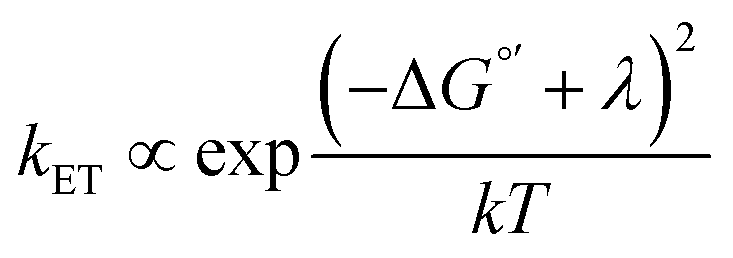 , where λ is the reorganization energy, k is the Boltzmann constant, and T is temperature.5–8 ΔG°′ is the standard driving force for interfacial electron transfer:
| ΔG°′ = ECB − qE°′ | (1) |
The specific problem is the 2D semiconductor energy levels move under working photocatalytic or photoelectrochemical conditions, due to both the applied potential (E)11–14 and absorption of photons.15–19 The phenomenon called band gap renormalization (BGR) involves movement of the semiconductor band edges, resulting in a potential- or light intensity-dependent ΔG°′ that currently remains unknown or ill-defined.13 The magnitude of BGR effects depend on the semiconductor's carrier concentration (n), which changes with applied potential or illumination. BGR effects are enormous in 2D semiconductors (e.g., >360 meV in photo-excited ML-MoS2)17 due to strong Coulomb interactions, dielectric screening effects, and quantum confinement.11–13,20–25 In the context of photoelectrochemistry, BGR shifts the semiconductor band edges dramatically upon illuminating or applying a potential to the semiconductor, changing ΔG°′ (see eqn (1)). Importantly, quantifying the extent to which applied potential, BGR, and other effects, such as illumination, tune the semiconductor band energies in these low dimensional materials remains a largely open question inspiring active research.13,26 In addition, the large band edge movement is significant because it violates a key assumption in the field of semiconductor electrochemistry: kET is essentially independent of E because the band edges are “fixed”.7 This assumption means ECB and EVB are independent of applied potential (E) and, therefore, ΔG°′ is independent of E, too. Thus, these assumptions fail for 2D semiconductors. There is a critical need to quantify interfacial energetics of 2D semiconductor/electrolyte interfaces so we can rationally tune the electron transfer kinetics of these systems for solar energy conversion applications.
Existing approaches and measurement techniques for quantifying interfacial energetics of bulk semiconductors cannot be directly applied to ultrathin 2D electrode materials. Hankin and co-workers discussed and compared popular methods: (1) Mott–Schottky (MS) analysis of differential capacitance versus potential data, (2) Gärtner–Butler (GB) analysis of photocurrent–potential data, and (3) determination of the transition potential between anodic and cathodic photocurrents under chopped illumination.27–30 Each method involves key assumptions to extract band edge positions. Those assumptions often fail even for bulk single crystal electrode materials and likely fail for 2D electrode materials as the material thickness becomes much thinner than the charge carrier depletion region thickness. For example, MS and GB analyses assume the applied potential manifests as a potential drop within the semiconductor's depletion region while the band edges remain fixed. As discussed above, large band edge movement is inherent to 2D semiconductor electrodes. The transition potential method between cathodic and anodic photocurrents interprets the transition potential as the flatband condition, where the band bending in the semiconductor is zero. Interpreting this potential as the flatband condition is problematic for 2D semiconductors because they have large (500 meV)11,31 exciton binding energies, and it is unclear how much additional electric field strength (i.e., applied potential) is required to overcome the binding energy and induce current flow near the zero-field condition. Another complicating factor is the exciton binding energies renormalize upon applying a potential to the 2D semiconductor. Extracting the electronic band gap (Eg) with optical measurements alone is problematic because we cannot assume the optical band gap and Eg renormalize equivalently in an electrolyte environment.32 Another practical experimental challenge for MS measurements is making defect-free 2D semiconductor/substrate contacts so the underlying metallic substrate does not contribute to the capacitance measurement. In summary, the methods for quantifying interfacial energetics of bulk semiconductor/electrolyte interfaces will most likely not be valid for 2D semiconductor electrodes.
Here we propose a new measurement approach to quantify the band edge movement of 2D semiconductor electrodes. Our optical approach involves the following steps: (1) measure potential-dependent absorbance spectra; (2) correlate carrier concentration (n) by matching the phenomenology of a many-body model to its predicted spectra; (3) interpolate the potential-dependent band gap energy based on first-principles-based effective-mass model calculations of the 2D semiconductor;33 and (4) construct an energy level diagram that quantifies BGR as a function of applied potential. The novel aspect of the approach is how it quantifies n via an easily accessible absorbance measurement (the 2D materials community routinely performs spatially resolved absorbance measurements).34 The Discussion section describes critical assumptions in steps 2–4 that currently limit the method to the model ML-MoS2 system, and pinpoints needed developments in experiment and theory to validate the approach for a wide range of 2D materials.
Results
In situ absorbance spectroscopy of ML-MoS2
We employ a widefield hyperspectral imaging method on an optical microscope to ensure our spectroelectrochemistry data stems from only ML-MoS2 material. Fig. 1A shows the experimental setup. A MoS2-coated ITO sample serves as the working electrode in an optically transparent three-electrode electrochemical cell (see Methods for detailed metal–organic chemical vapor deposition (MOCVD) MoS2 growth and subsequent wet transfer procedure). In a typical experiment, we immerse the ML-MoS2 sample in dry, N2-saturated acetonitrile electrolyte (0.25 M tetrabutylammonium hexafluorophosphate, [Bu4N][PF6]) and acquire hyperspectral image stacks at constant E by illuminating a microscopic 0.01 cm2 sample region with monochromatic light over the range of 400–700 nm in 2 nm increments (Fig. 1A). We chose this non-aqueous electrolyte to focus on how the BGR effect shifts the semiconductor band edges under non-electrocatalytic conditions. A 60× objective collects the transmitted light from the sample and projects it onto a sensitive sCMOS camera. Fig. 1B shows a representative bright field transmission image of the sample. The uniform image contrast across a large 1 mm2 area indicates the sample is predominantly ML-MoS2, as confirmed by Raman micro-spectroscopy measurements (Fig. S1, ESI†). However, microscopic defects such as tears, voids, wrinkles, and multilayer folds exist within the sample (see black arrows in Fig. 1B and Fig. S2, ESI†). Those defect features ordinarily contribute to and complicate the interpretation of ensemble-level electrochemical and optical data. | ||
| Fig. 1 (A) Cartoon illustration of the experimental setup (see main text and ESI† for detailed description). (B) Representative 10× bright field transmission image of the sample showing predominantly ML-MoS2 and some macroscopic defects. (C) 60× image of the sample edge. The yellow and red polygons show I0 and I ROIs for (λ) = log10(I0(λ)/I(λ)) calculations. | ||
To ensure our optical data stems from ML-MoS2 only, we spatially select regions of interest (ROIs) within each image that represent pristine ML-MoS2 and ITO (see Fig. 1C), and calculate A(l) = log10(I0(l)/I(l)), where I0(l) and I(l) are the monochromatic light intensities transmitted through the ITO substrate and ML-MoS2, respectively. In this way, we acquire spatially resolved in situ absorbance (A) data as a function of applied potential (E (V) vs. a calibrated Ag wire quasi-reference electrode (QRE), where E (V vs. Ag QRE) = E (V vs. NHE) − 0.498 V, see ESI† for calibration details). Crucially, this procedure removes the contributions from macroscopic defects in the sample. The uncertainty in A is <0.003 for measurements (see Fig. S3 in absorbance error analysis section in ESI†).
Fig. 2A shows representative absorbance spectra of ML-MoS2 from the hyperspectral imaging technique. Fig. S4 (ESI†) shows additional experimental data from multiple samples and for multiple potential cycles. We did not observe changes in Raman or absorbance spectra before or after experiments that would indicate significant chemical or structural transformation of the 2D electrode material (such as the 2H to 1T transition), in agreement with literature.13 However, in situ Raman spectroscopy measurements indicate the applied potential imparts a structural change in ML-MoS2 due to uniaxial tensile strain.13 The structural changes are apparently reversible, as evidenced by repeated Raman spectroscopy measurements. Regardless of the sample, the number of cycles, and the scan direction, we observed the following potential-dependent trends. First, the absorbance spectra at more positive potentials (light yellow trace in Fig. 2A) shows three distinct peaks at 655, 610, and 425 nm, which are attributed to the A, B, and C excitons, respectively.35 The A and B exciton peak intensities decrease and broaden with more negative potential (dark blue trace in Fig. 2A). On the other hand, the C exciton absorbance feature is essentially potential-independent (Fig. 2A-inset). Control experiments with bulk MoS2 material do not exhibit these dramatic spectral changes under the same electrochemical conditions (Fig. S5, ESI†).
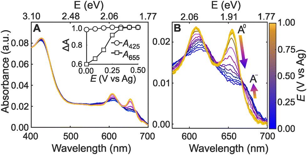 | ||
| Fig. 2 (A) Potential-dependent absorbance spectra of ML-MoS2 in 0.25 M [Bu4N][PF6] acetonitrile electrolyte. The inset highlights the A (655 nm) and C-exciton (425 nm) peak absorbance changes over a 500 mV potential range, where ΔA is absorbance normalized to the maximum value (ΔA = AV/Amax). (B) ML-MoS2 potential-dependent absorbance highlighting the A-exciton region with 50 mV steps. The arrows represent potential-dependent absorbance trends for A0 and A−. | ||
The potential-dependent trends in Fig. 2A agree with literature spectroelectrochemistry data for thin films of few-layer MoS2 nanosheets and colloidal film electrodes.13,26 However, little attention has been paid to the potential-dependent A-exciton lineshape for ML-MoS2 in liquid electrolyte. Fig. 2B shows potential-dependent spectra of the A-exciton peak for another ML-MoS2 sample using identical experimental conditions as Fig. 2A. Two distinct resonances contribute to this convoluted absorption feature.36 The neutral A-exciton absorbance (A0) dominates at more positive potentials. While at more negative potentials, the negatively charged trion (A−) dominates, resulting in a shoulder feature at 670 nm (see Fig. 2B). The spectral changes in Fig. 2 also occur in aqueous electrolyte and in potential regimes that are relevant to electrocatalytic hydrogen evolution (Fig. S6, ESI†). In the section that follows, we describe an approach to quantitatively link the measured absorbance spectrum to carrier concentration using a many-body model of minimal complexity to describe trion formation in ML transition metal dichalcogenides (TMDs) such as MoS2.37,38
MND model and fitting procedure to determine n
Here we adopt a minimal many-body model of a Fermi polaron put forth by Chang and Reichmann.37 Our implementation, based on the Mahan-Noziéres-De Dominicis (MND) Hamiltonian,39 computes the effective n that best describes the measured absorbance spectrum at each applied potential (E). The framework we develop herein can be generally applied to a wide range of 2D semiconductors and is not specific to ML-MoS2. A key feature of the model is its ability to capture how A0 and A− resonances shift in energy and transfer oscillator strength between one another as a function of carrier doping concentration. Before we discuss the detailed calculation and fitting procedures, we first describe the predictions of the MND model at positive, intermediate, and negative potentials.The MND model considers the MoS2 sample is an n-doped 2D semiconductor,40,41 where the majority carriers are conduction band electrons. In the experiment, the external power supply modulates the carrier population. For an unbiased sample at T = 0 K, the model assumes the Fermi level is below the conduction band minimum and the A-exciton absorbance saturates. Consistent with this expectation, we observe A0 absorbance saturation at positive applied potentials (e.g., E > 0.7 V, Fig. S4, ESI†). At this undoped condition (Fig. 3A), the MND model predicts two peaks for the A0 and A− transitions (dashed and dotted lines in Fig. 3A and B). The oscillator strength is mostly associated with the higher energy A0 transition, as indicated by the thick black line in Fig. 3A. After convolving the calculated A0 and A− linewidths to account for Gaussian broadening and the instrument response, we obtain a single broad peak at 1.894 eV (solid line in Fig. 3B). The key point here is that the experimentalist observes a single absorbance peak at positive potentials because the oscillator strength is mostly associated with A0 at lower n.
 | ||
| Fig. 3 (A)–(F) Cartoon illustration of ML-MoS2 electronic structure changes predicted by the MND model. (A) Electronic band gap energy (Eg), neutral A-exciton energy (EA0) and negatively charged trion energy ((EA−)) at the low doping condition (e.g., 1.00 V). (B) Simulated absorbance spectrum (solid line) predicted from the exciton and trion contributions (dashed and dotted lines, respectively). (C) and (D) same as (A) and (B)) but for intermediate potentials/intermediate n. (E) and (F) same as (A) and (B), but for most negative potentials/highest n. (G) Simulated and optimized absorbance spectra (solid lines) for each experimentally measured spectrum (circles). | ||
The situation changes as n increases. The MND model predicts oscillator strength transfers from A0 to A−, as indicated by thicker lines for the A− transition in Fig. 3EversusFig. 3A and C. The oscillator strength shift changes the A0![[thin space (1/6-em)]](https://www.rsc.org/images/entities/char_2009.gif) :A− intensity ratio and the peak energy shifts complicate the observed spectrum. As the applied potential shifts from positive to negative, the experimentalist observes a “super peak” split into two discernable peaks (see convolved spectrum in Fig. 3D). A key point of Fig. 3A–F is that the MND model predicts how and why the “super peak” absorbance feature at low n (positive potentials) transitions to two separate peaks at high n (negative potentials).
:A− intensity ratio and the peak energy shifts complicate the observed spectrum. As the applied potential shifts from positive to negative, the experimentalist observes a “super peak” split into two discernable peaks (see convolved spectrum in Fig. 3D). A key point of Fig. 3A–F is that the MND model predicts how and why the “super peak” absorbance feature at low n (positive potentials) transitions to two separate peaks at high n (negative potentials).
Having summarized the general predictions of the model, we can now discuss the general fitting procedure to determine n at each E for the experimental data in Fig. 2. Our previous work provides complete MND model calculation details.38 Briefly, the model quantitatively links the experimental observable (absorbance spectrum) to n via the Fermi doping energy parameter εF, defined as an energy level position at or above the conduction band minimum.37,42 First, we obtain model parameters, the undoped A0 peak (i.e., energy, width, and height), using data acquired at E = +1.00 V and account for phenomenological peak broadening by convolving the simulated peak with a Gaussian. Then, for all other more negative E values (i.e., higher εF conditions), we make an initial guess at the parameters for both A0 and A− and perform a 5-step procedure to determine εF for every E (see ESI† for details). The rationale of the steps is to model the data globally at the level of the MND peak lineshape outputs instead of guessing at the correct Hamiltonian. We can infer an effective doping density from the ratio of peak heights in the experimental absorbance data based on the series of spectra predicted from the MND model.
Fig. 3G shows the results of the fitting procedure applied to the absorbance spectra in Fig. 2B. The model captures all potential-dependent features of the A-exciton region, specifically how the A0 and A− peak intensities, positions, and widths change with applied potential. A key point of Fig. 3G is we obtain a single εF value that best describes each measured spectrum. Minor disagreement between the MND model and experimental data, such as the high energy tail region, is likely because the MND model only considers the pristine ML-MoS2 sample in vacuum and does not consider the possible screening effects from the substrate and liquid electrolyte. Disagreement between the theory and experiment may also be due to non-Gaussian sources of broadening that we do not consider, as well as the simple background subtraction method that does not accurately remove contributions from the B exciton and B trion,43 which the model does not consider.
Having determined εF for each E, we then calculate n. Chang and Reichman applied the MND Hamiltonian to ML-MoS2 to calculate n (in units of cm−2) assuming a parabolic band structure:
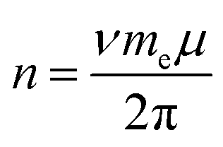 | (2) |
Fig. 4 shows calculated n values versus E. n remains low for E > +0.50 V. Then, n abruptly increases by an order of magnitude over a narrow range (0.30 to 0.50 V). n steadily increases with increasingly negative potentials (E < 0.20 V). For comparison, we also calculated n values using the approach of Carroll et al.,13 who adapted Wannier–Mott (WM) effective mass theory for 2D quantum wells44,45 to calculate n for 2D materials (see WM model calculations section in ESI† for details). Notably, the WM model does not consider the potential-dependent A− feature and, therefore, the A-exciton region of the absorbance spectrum is fitted with a single component Gaussian. The n values in Fig. 4 differ by an order of magnitude but show qualitatively similar behavior. The n values calculated from the MND model are likely lower because the approach ignores thermal contributions to n and, therefore, likely underestimates the true concentration of conduction band electrons. On the other hand, the n values calculated from the Wannier–Mott model sensitively depend on the exciton Bohr radius (n ∝ a0−2), which linearly depends on me.46 Varying a0 (or me) by a factor of 3 results in nearly an order of magnitude change in n (Fig. S7, ESI†). While it is difficult to know at this stage what the true n values are, the remarkable qualitative agreement using two different approaches indicate that the n–E trends observed in Fig. 4 are robust.
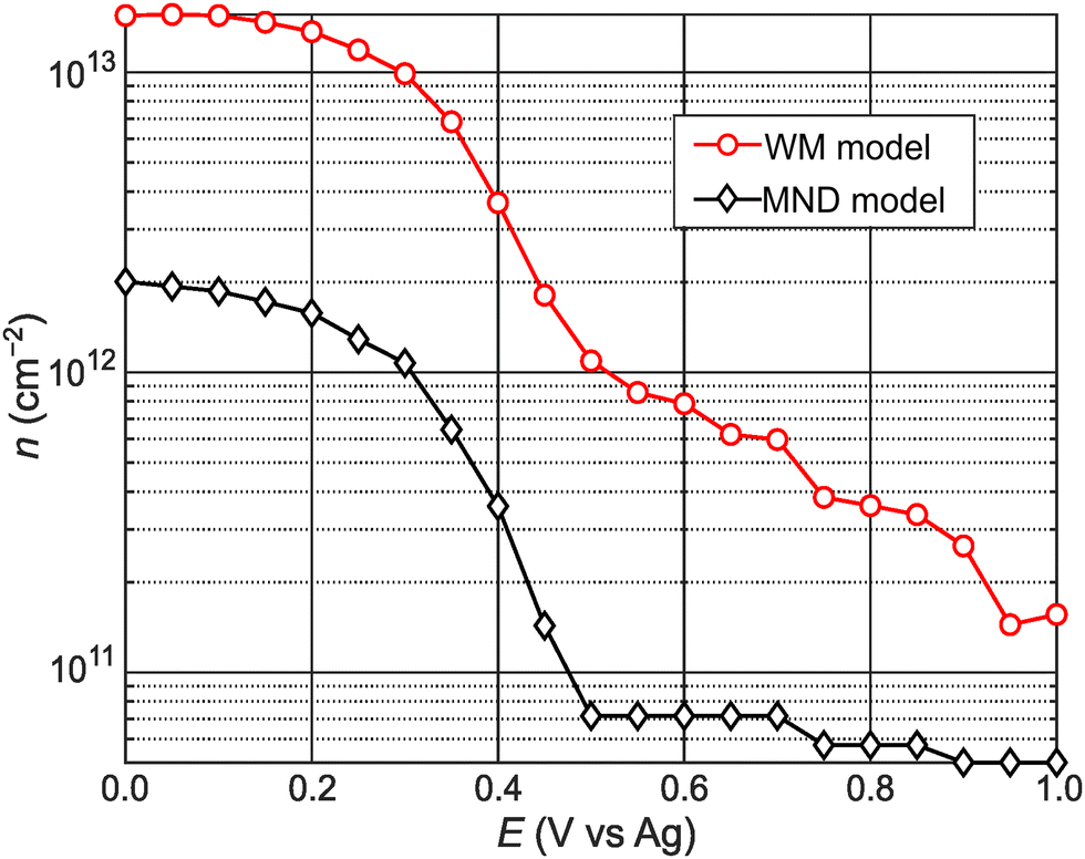 | ||
| Fig. 4 Potential-dependent carrier concentration values calculated via the MND (black diamonds) and WM model (red circles). | ||
Band energy diagram construction
Finally, we construct a band energy diagram for the ML-MoS2 electrode using the following assumptions. First, we interpolate n-dependent Eg values from first-principles-based effective-mass model calculations33 (see Fig. S8, ESI†). Second, we pin the conduction band edge of ML-MoS2 at 4.2 V vs. the vacuum scale47 (or −0.3 V vs. NHE) and assume BGR only shifts the valence band, in agreement with time and angle-resolved photoelectron spectroscopy (TR-ARPES) measurements.17 Therefore, we position the VB edge relative to the fixed CB edge using the n-dependent Eg values.Fig. 5 shows the resulting band energy diagrams of ML-MoS2 as a function of applied voltage using n-dependent Eg values interpolated from Gao et al.33 Note, we constructed two energy level diagrams using n values obtained from the MND and WM models. At positive potentials, Eg approaches the value predicted for “undoped” ML-MoS2 (see Fig. 5 inset). Eg decreases with increasingly negative E, causing the VB minimum to shift by over 200 meV over a narrow E range. The Eg decrease (and upward VB shift) is greater for larger values of n, such as those predicted by the WM model (see red circles in Fig. 5). Note, the WM model does not consider the unique many body physics of 2D semiconductors (e.g., bandgap renormalization, trion formation, screening of quasiparticle binding energies). Fig. S9 (ESI†) shows an additional band energy diagram using experimental Eg values obtained from TR-ARPES measurements;17 the quantitative values differ slightly, but the qualitative trends hold. The key point of Fig. 5 is that BGR effects cause significant band edge movement (0.2–0.5 eV) and should be given consideration when designing 2D electrodes for electrochemical applications, as will be discussed more below. Importantly, the majority of the BGR shown here occurs over a remarkably narrow range of applied potentials.
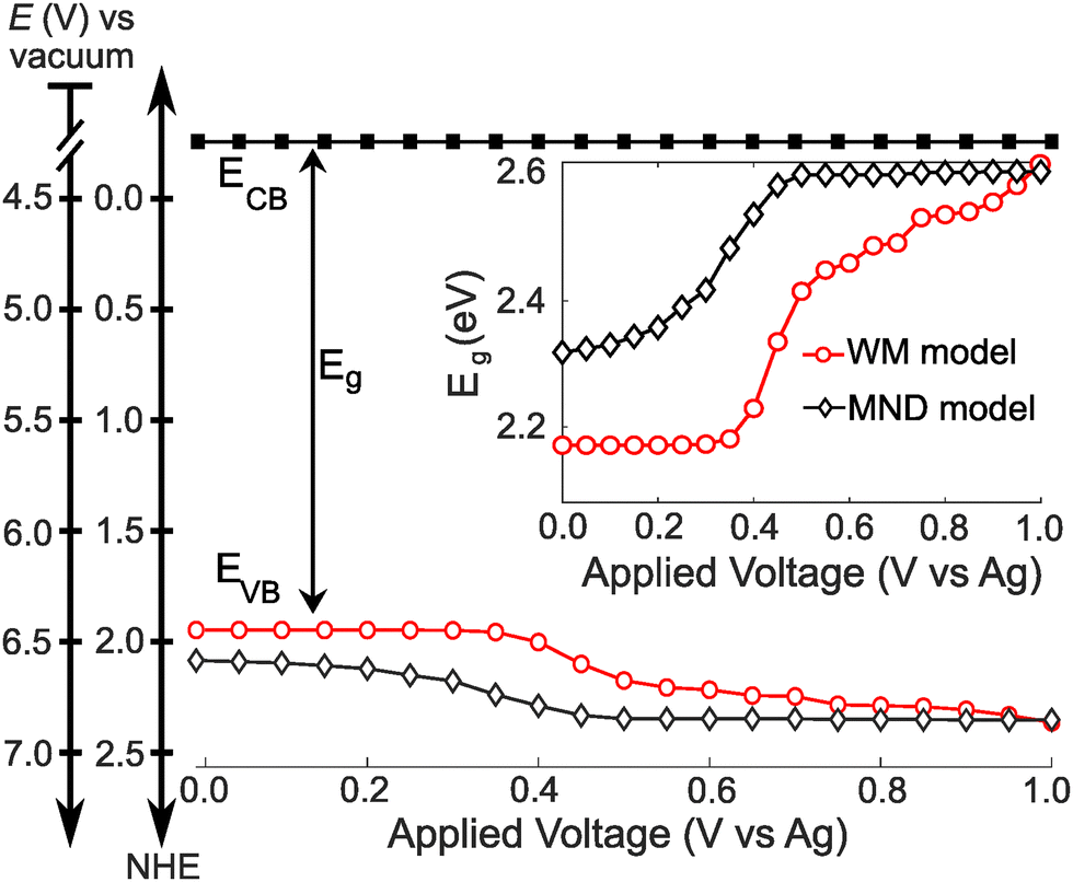 | ||
| Fig. 5 Band energy diagram of ML-MoS2 as a function of E in a 0.25 M [Bu4N][PF6] acetonitrile electrolyte. The inset shows the band gap energy as a function of E. | ||
Discussion
The enormous BGR effect in 2D semiconductors has important consequences for any electrochemical application involving interfacial charge transfer. The large band edge energy shifts (0.5 eV) can occur over a narrow range of applied potentials (0.2–0.3 V). In turn, the fundamental driving force for the reaction ΔG°′ changes dramatically. From a kinetic standpoint, the large band edge movements will dramatically affect interfacial charge transfer rates. If the electron transfer rate constant kET follows a Marcus-Gerischer relationship, where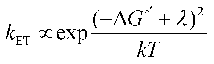 , then large ΔG°′ changes (e.g., 0.5 eV) could change kET by a factor of 10–100.9,10 It is even possible that ΔG°′ changes sign if the VB/CB edge moves above/below E°′. This means the (photo)electrocatalytic reaction could transition from being spontaneous in one potential regime to non-spontaneous in another. Note, our study focused only on BGR effects caused by the applied potential. For light-driven reactions in a photoelectrosynthetic cell, the band edge movement will be driven by the applied bias and the photogenerated carrier population,48 further complicating the interfacial energetics. One could envision leveraging this kinetic or thermodynamic information to design an “electrochemical switch” for a desired reaction.
We now discuss key assumptions in the proposed approach and point out clear next steps to make this approach more robust with future advances in experiment and theory. First, our experimental method does not directly measure band edge positions. We assumed a potential-independent CB minimum value for this model ML-MoS2 system, which may not be valid for all 2D materials and those that have yet to be discovered. New in situ methods are needed to determine band edge positions of the 2D electrode. Direct measurement of CB and VB edges yield Eg, which could be compared to the Eg values we extract from in situ absorbance measurements.
Second, we quantify band edge movement by interpolating Eg values as a function of n. The first problem with this strategy is the accuracy of n values obtained using either the MND or WM models. We calculate n from the εF parameter in the MND model using eqn (2), which considers the pristine semiconductor at 0 K. Aside from ignoring the thermally excited carriers, the MND model does not consider the electrolyte, underlying substrate, spin–orbit coupling to treat the B-exciton and B-trion,43 and defects that could serve as extrinsic dopants in the 2D material. A growing body of evidence has shown that defect concentrations and types,49,50 substrate materials,31,51 solvent,52,53 and surrounding chemical environment54 all influence n. Current theory does not consider many practical materials and electrochemical factors. Future theory development is needed to accurately determine n using in situ spectroelectrochemistry (e.g., absorbance/reflectance, Raman, or PL spectroscopy). The second problem with the optical spectroscopy strategy proposed herein is it relies also on the accuracy of Eg values as a function of n. Experimentally measured Eg values17 show similar BGR trends as the theoretical calculations,33,55 but the absolute values can differ by as much as 0.2 eV. The disagreement could be due to the fact the models do not consider defects and substrate/environmental doping effects. Despite the current difficulty in precisely assigning n and Eg, we believe in situ absorbance measurements, modelled by many-body theory instead of the WM model, represent a viable approach to quantify interfacial energetics because there is a robust theoretical framework connecting the observed spectrum to critical parameters relevant to semiconductor energy levels (n and Eg).
One clear advantage of our proposed approach is experimental simplicity. Commercially available UV-vis spectrophotometers have absorbance resolution ≤0.001, which is an order of magnitude lower than exciton absorbance peak values of ultrathin TMD semiconductors (Fig. 2). However, large area, defect-free samples are required for benchtop absorbance measurements. Ensemble-average measurements in a benchtop instrument report on the average behaviour of the entire sample in the light path, which could include defects and pinholes in the material as shown in Fig. 1 and Fig. S2 (ESI†). We argue the advantages and disadvantages of the optical approach proposed herein are similar to the popular Mott–Schottky method for bulk semiconductor/electrolyte interfaces; Mott–Schottky data is easy to acquire but can be difficult to interpret.27 The current approach (modelling absorbance data using many body theory) can be rapidly applied to any 2D semiconductor in the TMD family.
Conclusion
In summary, we developed an all-optical approach to quantify the interface energetics of ML-MoS2 semiconductor–electrolyte interfaces. The method involves (1) measuring potential-dependent absorbance spectra; (2) fitting the neutral exciton and trion features in the absorbance spectrum using the MND model to extract the carrier concentration n; (3) interpolating the electronic band gap at each E using n; (4) constructing an energy level diagram assuming a known, potential-independent CB edge value. Our results show that band edge movement in ML-MoS2 is significant (0.2–0.5 eV) over a narrow range of applied potentials (0.2–0.3 V). The band edge movement magnitude depends on the calculated n values. Large band edge shifts have important consequences for practical electrochemical applications involving interfacial charge transfer because kET could change by a factor of 10–100. Future experimental and theoretical work is needed to accurately measure n from in situ spectroelectrochemical measurements such as absorbance/reflectance, Raman, or PL spectroscopy.ML-MoS2 synthesis and transfer
ML-MoS2 films were grown via MOCVD on sapphire substrates according to Sebastian et al.56 Molybdenum hexacarbonyl (Mo(CO)6) and hydrogen sulfide (H2S) served as the Mo and S sources. H2 served as the carrier gas. The samples were transfer to a 25 mm × 75 mm × 1.1 mm ITO coated glass substrates (Delta Technologies Part No. CB-40IN-S111, Rs = 4–10 Ω) using a polymethyl-methacrylate (PMMA)-assisted wet transfer process.57 First, PMMA (IMM, 495K A5) was spin-coated on the ML-MoS2 covering the sapphire substrate. The PMMA-coated sample was immersed in a 1 M NaOH solution at 70 °C to separate the PMMA/ML-MoS2 film from the sapphire substrate. The separated film was then rinsed multiple times inside a water bath and finally transferred onto the target ITO substrate. The rinsed film was lifted from the water bath using the ITO and dried with N2 gas.In situ spectroelectrochemistry
We constructed a transparent three-electrode microfluidic electrochemical cell according to Wang et al.58 Electrolyte flowed through the cell at a constant rate of 50 μL min−1 using an automated syringe pump. The electrolyte was sparged (and later blanketed) with N2 gas for at least 30 min prior to flowing through the electrochemical cell. The electrochemical cell was mounted on the stage of an inverted optical microscope (Olympus IX73) where a 60× objective UPLANSAPO60×/W) focused light onto a sCMOS camera (Teledyne Prime 95B). An Ivium Compactstat Potentiostat applied a constant potential during each spectral measurement using a Pt wire counter electrode and Ag wire quasi-reference electrode. A Horiba OBB monochromator (1200 g mm−1, 1.2 mm slit) selected light from a Xe lamp source in 2 nm wavelength steps. A(λ) was calculated for each respective image with I and I0 ROI boundaries for each set of potential-dependent spectral data. Each A(λ) is the average of measurements from 12 to 16 images. The absorbance data was collected using non-sequential applied potentials. A data acquisition system (DATAQ 4108) synchronized the camera, monochromator, and potentiostat signals. The ESI† provides further experimental details and imaging procedures.Conflicts of interest
There are no conflicts to declare.Acknowledgements
This research was supported by the U.S. Department of Energy, Office of Science, Office of Basic Energy Sciences, under Award DE-SC0021189 (JBS, RA, RA), and under Award DE-SC0016137 (ATK, YRF). JBS acknowledges a Sloan Research Fellowship (Grant Number FG-2022-18405). JT acknowledges the Army Advanced Civil Schooling Program for a graduate research fellowship. The samples were grown in the 2D Crystal Consortium Materials Innovation Platform (2DCC-MIP) facility at Penn State which is supported by the National Science Foundation under cooperative agreement DMR-2039351. This material is based upon work supported by the National Science Foundation Graduate Research Fellowship Program under grant no. DGE1255832 (NT).References
- A. J. Nozik, D. S. Boudreaux, R. R. Chance and F. Williams, Interfacial Photoprocesses: Energy Conversion and Synthesis, American Chemical Society, 1980, vol. 184, pp. 155–171 Search PubMed.
- D. S. Boudreaux, F. Williams and A. J. Nozik, J. Appl. Phys., 1980, 51, 2158 CrossRef CAS.
- G. Cooper, J. A. Turner, B. A. Parkinson and A. J. Nozik, J. Appl. Phys., 1983, 54, 6463 CrossRef CAS.
- R. Austin, Y. R. Farah, T. Sayer, B. M. Luther, A. Montoya-Castillo, A. T. Krummel and J. B. Sambur, Proc. Natl. Acad. Sci. U. S. A., 2023, 120, e2220333120 CrossRef CAS PubMed.
- H. Gerischer, in Physical Chemstry: An Advanced Treatise, ed. H. Eyring, D. Henderson and W. Jost, Academic, New York, 1970, vol. IXA Search PubMed.
- R. A. Marcus and N. Sutin, Biochim. Biophys. Acta, 1985, 811, 265–322 CrossRef CAS.
- N. S. Lewis, Annu. Rev. Phys. Chem., 1991, 42, 543–580 CrossRef CAS.
- D. B. Sulas-Kern, E. M. Miller and J. L. Blackburn, Energy Environ. Sci., 2020, 13, 2684–2740 RSC.
- T. W. Hamann, F. Gstrein, B. S. Brunschwig and N. S. Lewis, J. Am. Chem. Soc., 2005, 127, 7815–7824 CrossRef CAS PubMed.
- T. W. Hamann, F. Gstrein, B. S. Brunschwig and N. S. Lewis, Chem. Phys., 2006, 326, 15–23 CrossRef CAS.
- M. M. Ugeda, A. J. Bradley, S.-F. Shi, F. H. da Jornada, Y. Zhang, D. Y. Qiu, W. Ruan, S.-K. Mo, Z. Hussain, Z.-X. Shen, F. Wang, S. G. Louie and M. F. Crommie, Nat. Mater., 2014, 13, 1091–1095 CrossRef CAS PubMed.
- A. Chernikov, A. M. van der Zande, H. M. Hill, A. F. Rigosi, A. Velauthapillai, J. Hone and T. F. Heinz, Phys. Rev. Lett., 2015, 115, 126802–126806 CrossRef PubMed.
- G. M. Carroll, H. Zhang, J. R. Dunklin, E. M. Miller, N. R. Neale and J. van de Lagemaat, Energy Environ. Sci., 2019, 140, 441–449 Search PubMed.
- P. V. Nguyen, N. C. Teutsch, N. P. Wilson, J. Kahn, X. Xia, A. J. Graham, V. Kandyba, A. Giampietri, A. Barinov, G. C. Constantinescu, N. Yeung, N. D. M. Hine, X. Xu, D. H. Cobden and N. R. Wilson, Nature, 2019, 572, 220–223 CrossRef CAS PubMed.
- A. Chernikov, C. Ruppert, H. M. Hill, A. F. Rigosi and T. F. Heinz, Nat. Photonics, 2015, 9, 466–470 CrossRef CAS.
- Y. Park, S. Wook Han, C. C. S. Chan, B. P. L. Reid, R. A. Taylor, N. Kim, Y. Jo, H. Im and K. S. Kim, Nanoscale, 2017, 9, 10647–10652 RSC.
- F. Liu, M. E. Ziffer, K. R. Hansen, J. Wang and X. Zhu, Phys. Rev. Lett., 2019, 122, 246803 CrossRef CAS PubMed.
- Y. Wang, Z. Nie and F. Wang, Light Sci. Appl., 2020, 9, 192 CrossRef CAS PubMed.
- Y. Lin, Y. Chan, W. Lee, L.-S. Lu, Z. Li, W.-H. Chang, C.-K. Shih, R. A. Kaindl, S. G. Louie and A. Lanzara, Phys. Rev. B: Condens. Matter Mater. Phys., 2022, 106, L081117 CrossRef CAS.
- D. Y. Qiu, F. H. da Jornada and S. G. Louie, Phys. Rev. Lett., 2013, 111, 216805 CrossRef PubMed.
- A. Kuc and T. Heine, Chem. Soc. Rev., 2015, 44, 2603–2614 RSC.
- E. J. Sie, A. J. Frenzel, Y.-H. Lee, J. Kong and N. Gedik, Phys. Rev. B: Condens. Matter Mater. Phys., 2015, 92, 125417 CrossRef.
- B. Liu, W. Zhao, Z. Ding, I. Verzhbitskiy, L. Li, J. Lu, J. Chen, G. Eda and K. P. Loh, Adv. Mater., 2016, 28, 6457–6464 CrossRef CAS PubMed.
- S. Gao, Y. Liang, C. D. Spataru and L. Yang, Nano Lett., 2016, 16, 5568–5573 CrossRef CAS PubMed.
- K. Yao, A. Yan, S. Kahn, A. Suslu, Y. Liang, E. S. Barnard, S. Tongay, A. Zettl, N. J. Borys and P. J. Schuck, Phys. Rev. Lett., 2017, 119, 087401–087406 CrossRef PubMed.
- K. M. Wurst, O. Strolka, J. Hiller, J. Keck, A. J. Meixner, J. Lauth and M. Scheele, Small, 2023, 2207101 CrossRef CAS PubMed.
- A. Hankin, F. E. Bedoya-Lora, J. C. Alexander, A. Regoutz and G. H. Kelsall, J. Mater. Chem. A, 2019, 7, 26162–26176 RSC.
- F. Cardon and W. P. Gomes, J. Phys. Appl. Phys., 1978, 11, L63–L67 CrossRef CAS.
- R. Memming and G. Schwandt, Angew. Chem., Int. Ed. Engl., 1967, 6, 851–861 CrossRef CAS.
- M. A. Butler, J. Appl. Phys., 1977, 48, 1914 CrossRef CAS.
- A. Raja, A. Chaves, J. Yu, G. Arefe, H. M. Hill, A. F. Rigosi, T. C. Berkelbach, P. Nagler, C. Schüller, T. Korn, C. Nuckolls, J. Hone, L. E. Brus, T. F. Heinz, D. R. Reichman and A. Chernikov, Nat. Commun., 2017, 8, 15251 CrossRef PubMed.
- A. Chaves, J. G. Azadani, H. Alsalman, D. R. da Costa, R. Frisenda, A. J. Chaves, S. H. Song, Y. D. Kim, D. He, J. Zhou, A. Castellanos-Gomez, F. M. Peeters, Z. Liu, C. L. Hinkle, S.-H. Oh, P. D. Ye, S. J. Koester, Y. H. Lee, P. Avouris, X. Wang and T. Low, npj 2D Mater. Appl., 2020, 4, 29 CrossRef CAS.
- S. Gao and L. Yang, Phys. Rev. B, 2017, 96, 155410 CrossRef.
- R. Frisenda, Y. Niu, P. Gant, A. J. Molina-Mendoza, R. Schmidt, R. Bratschitsch, J. Liu, L. Fu, D. Dumcenco, A. Kis, D. P. De Lara and A. Castellanos-Gomez, J. Phys. Appl. Phys., 2017, 50, 074002–074009 CrossRef.
- J. A. Wilson and A. D. Yoffe, Adv. Phys., 1969, 18, 193–335 CrossRef CAS.
- K. F. Mak, K. He, C. Lee, G. H. Lee, J. Hone, T. F. Heinz and J. Shan, Nat. Mater., 2013, 12, 207–211 CrossRef CAS PubMed.
- Y.-W. Chang and D. R. Reichman, Phys. Rev. B, 2019, 99, 125421 CrossRef CAS.
- T. Sayer, Y. R. Farah, R. Austin, J. Sambur, A. T. Krummel and A. Montoya-Castillo, Nano Lett., 2023, 23, 6035–6041 CrossRef CAS PubMed.
- G. D. Mahan, Many-Particle Physics, Springer US, Boston, MA, 2000 Search PubMed.
- K. Kang, S. Xie, L. Huang, Y. Han, P. Y. Huang, K. F. Mak, C.-J. Kim, D. Muller and J. Park, Nature, 2015, 520, 656–660 CrossRef CAS PubMed.
- A. Sebastian, R. Pendurthi, T. H. Choudhury, J. M. Redwing and S. Das, Nat. Commun., 2021, 12, 693 CrossRef CAS PubMed.
- G. V. Astakhov, V. P. Kochereshko, D. R. Yakovlev, W. Ossau, J. Nürnberger, W. Faschinger and G. Landwehr, Phys. Rev. B: Condens. Matter Mater. Phys., 2000, 62, 10345–10352 CrossRef CAS.
- M. Drüppel, T. Deilmann, P. Krüger and M. Rohlfing, Nat. Commun., 2017, 8, 2117 CrossRef PubMed.
- D. Huang, J.-I. Chyi and H. Morkoç, Phys. Rev. B: Condens. Matter Mater. Phys., 1990, 42, 5147–5153 CrossRef CAS PubMed.
- T. Cheiwchanchamnangij and W. R. L. Lambrecht, Phys. Rev. B: Condens. Matter Mater. Phys., 2012, 85, 205302 CrossRef.
- C. Zhang, H. Wang, W. Chan, C. Manolatou and F. Rana, Phys. Rev. B: Condens. Matter Mater. Phys., 2014, 89, 205436 CrossRef.
- J. E. Padilha, H. Peelaers, A. Janotti and C. G. Van de Walle, Phys. Rev. B: Condens. Matter Mater. Phys., 2014, 90, 205420 CrossRef.
- E. A. A. Pogna, M. Marsili, D. De Fazio, S. Dal Conte, C. Manzoni, D. Sangalli, D. Yoon, A. Lombardo, A. C. Ferrari, A. Marini, G. Cerullo and D. Prezzi, ACS Nano, 2016, 10, 1182–1188 CrossRef CAS PubMed.
- R. Addou, L. Colombo and R. M. Wallace, ACS Appl. Mater. Interfaces, 2015, 7, 11921–11929 CrossRef CAS PubMed.
- S. McDonnell, R. Addou, C. Buie, R. M. Wallace and C. L. Hinkle, ACS Nano, 2014, 8, 2880–2888 CrossRef CAS PubMed.
- M. Buscema, G. A. Steele, H. S. J. van der Zant and A. Castellanos-Gomez, Nano Res., 2014, 7, 561–571 CrossRef.
- N. Mao, Y. Chen, D. Liu, J. Zhang and L. Xie, Small, 2013, 9, 1312–1315 CrossRef CAS PubMed.
- Y. Lin, X. Ling, L. Yu, S. Huang, A. L. Hsu, Y.-H. Lee, J. Kong, M. S. Dresselhaus and T. Palacios, Nano Lett., 2014, 14, 5569–5576 CrossRef CAS PubMed.
- S. Tongay, J. Zhou, C. Ataca, J. Liu, J. S. Kang, T. S. Matthews, L. You, J. Li, J. C. Grossman and J. Wu, Nano Lett., 2013, 13, 2831–2836 CrossRef CAS PubMed.
- Y. Liang and L. Yang, Phys. Rev. Lett., 2015, 114, 063001 CrossRef CAS PubMed.
- A. Sebastian, R. Pendurthi, T. H. Choudhury, J. M. Redwing and S. Das, Nat. Commun., 2021, 12, 693 CrossRef CAS PubMed.
- F. Zhang, C. Erb, L. Runkle, X. Zhang and N. Alem, Nanotechnology, 2017, 29, 025602 CrossRef PubMed.
- L. Wang and J. B. Sambur, Nano Lett., 2019, 19, 2960–2967 CrossRef CAS PubMed.
Footnotes |
| † Electronic supplementary information (ESI) available. See DOI: https://doi.org/10.1039/d3ee01165h |
| ‡ These authors contributed equally to this work. |
| This journal is © The Royal Society of Chemistry 2023 |