
Solid–solid chemical bonding featuring targeted defect passivation for efficient perovskite photovoltaics†
Chao
Luo
a,
Guanhaojie
Zheng
bcd,
Xianjin
Wang
a,
Feng
Gao
a,
Changling
Zhan
a,
Xingyu
Gao
 bcd and
Qing
Zhao
*aef
bcd and
Qing
Zhao
*aef
aState Key Lab for Mesoscopic Physics and Frontiers Science Center for Nano-optoelectronics, School of Physics, Peking University, Beijing, 100871, China. E-mail: zhaoqing@pku.edu.cn
bShanghai Synchrotron Radiation Facility (SSRF), Zhangjiang Lab, Shanghai Advanced Research Institute, Chinese Academy of Sciences, Shanghai 201204, China
cUniversity of Chinese Academy of Sciences, Beijing 100049, China
dShanghai Institute of Applied Physics, Chinese Academy of Sciences, Shanghai 201800, China
ePeking University Yangtze Delta Institute of Optoelectronics, Nantong, 226010, Jiangsu, China
fCollaborative Innovation Center of Quantum Matter, Beijing, 100084, China
First published on 1st December 2022
Abstract
Solution-processed surface defect passivation has enabled perovskite solar cells (PSCs) to make remarkable progress in recent years. Here, different from solution processing, we proposed solvent-free solid-phase passivation (SPP) to bond surface uncoordinated Pb2+ defects using passivator molecules on pre-prepared solid-state films. The attentively selected passivator was found to anchor on the defect sites of the perovskite film surface even if the passivator film was removed, due to its strong coordination ability with the uncoordinated Pb2+ defects. This unique targeted defect passivation substantially reduces the carrier non-radiative recombination loss, delivering a high VOC of 1.20 V (voltage loss is only 0.34 V). Consequently, the power conversion efficiency (PCE) of PSCs was greatly improved from 22.37% to certified 24.65%. The 1 cm2 SPP-based PSC also exhibited a high PCE exceeding 23%. Moreover, the unencapsulated PSCs maintain 98% and 92% of their initial efficiency after storage under nitrogen for 2300 h and tracking at a maximum power point for 800 h.
Broader contextAs the latest generation of photovoltaic technology, low-cost and efficient perovskite solar cells (PSCs) are attracting extensive interest from the scientific community and the capital market. Effective passivation of the defects generated during the preparation process is a crucial prerequisite for obtaining high-performance PSCs. Further development of perovskite photovoltaics requires a more effective defect passivation management strategy. In this study, we proposed a solvent-free solid-phase passivation strategy to efficiently bond uncoordinated defects on the surface of perovskite films by the carefully selected passivator molecules, which can dramatically reduce the non-radiative recombination loss of carriers. Moreover, this method features targeted defect passivation, that is, only passivating the defect sites but not affecting the benign regions without defects. In addition, one solid-state passivator substrate can be used many times to manufacture multiple high-efficiency PSCs. This strategy can overcome some of the difficulties faced by the current solution-processed defect passivation, so we expect that this technology can promote the further development of PSCs. |
Introduction
Perovskite solar cells (PSCs) have emerged as a promising candidate for next-generation photovoltaic applications,1–4 due to the superior optoelectronic properties of metal halide perovskite materials.5–11 The soft ionic nature of solution-processed perovskites inevitably makes the obtained perovskite films suffer from a large number of defects,12–14 which are mainly distributed on the film surface and grain boundary,15 resulting in serious non-radiative carrier recombination.6,16–18 In addition, these surface defects also facilitate the entry of water and oxygen into the film resulting in the beginning of film degradation.19,20 Therefore, reviewing the development of PSCs, massive research efforts have been dedicated to develop various surface defect passivation strategies for markedly enhancing the efficiency and stability of PSCs.21–23 Among them, the solution-processed method played a dominant role, even in the record-breaking PSCs in recent years.21,24,25 For example, very recently, Jiang et al. obtained a record efficiency of 25.37% for inverted PSCs based on solution-processed surface treatment.26 Nevertheless, there are still several points that need to be carefully considered in solution-processed surface passivation.27 First, surface passivation by the solution method inevitably encounters certain challenges regarding compatibility with larger sizes beyond the capabilities of spin-coating. Second, the selection range of passivators may encounter certain restrictions considering that the passivator should be dissolved in a specific solvent that will not devastatingly destroy the underlying perovskite films, usually isopropanol (IPA) or chlorobenzene (CB). Moreover, the solution method may also cause a slight surface component disruption (affect the stoichiometric ratio of the perovskite film surface) of the surface passivator residue due to the indiscriminate coverage of the passivator.In this sense, a solution-free, solid-phase method may hold great potential in solving the above challenges. In general, the solid-phase method possesses inherent superiority over the solution method, such as size compatible capability, freedom of passivator selection (independent of solvent consideration), and a minimum surface passivator residue (more detailed elaborations are summarized in Note S1 and Fig. S1, ESI†). Recently, a solid-phase in-plane growth method at high pressure was applied to prepare a highly pure two-dimensional (2D) perovskite on the surface of a three-dimensional (3D) perovskite film,28 resulting in a local electric field at the 2D/3D heterojunction, and thus an improved efficiency of PSCs of 24.35%. This work pays valuable attention to the preparation of 2D perovskites at high pressure. In addition, Zhang et al. stacked two solid state perovskite films (FAPbI3 and MAPbI3) face to face to perform low-temperature annealing to obtain high-efficiency PSCs via DMSO-mediated ion exchange.29 However, the research on solid-phase passivation via a coordination chemistry interaction is currently missing. Exploration of solid-phase passivation would be fundamentally meaningful in understanding solid-solid defect passivation mechanisms and exploiting more practical passivation approaches towards efficient PSCs.
In this work, we devised a solid-phase passivation (SPP) method for efficient surface defect passivation aiming for high-efficiency PSCs. The passivator with strong coordination ability was pre-prepared as a film on a solid substrate. Then the passivator film was vertically covered on the upper surface of the as-prepared perovskite film under heat and pressure conditions. Solid–solid chemical bonding was formed via a coordination bond between the passivator molecule and uncoordinated Pb2+ on the surface of the perovskite film. Such a bonding keeps the passivator anchored on the Pb2+ defect sites, even if the passivator film substrate was detached. For defect-free regions, the passivator will be removed together with the passivator substrate since there is no strong interaction between the perovskite surface and the passivator molecules, thereby avoiding the surface residue of the passivator. This unique targeted solid-phase defect passivation dramatically enhances the efficiency of PSCs to certified 24.65%. The corresponding large-area solar cells (1 cm2) achieved a high PCE of 23%. Moreover, the unencapsulated PSCs retained 98% of their initial PCE after storing in nitrogen for more than 2300 hours and maintained 92% of their initial PCE after tracking at the maximum power point (MPP) under continuous 1 sun illumination for 800 h.
Results and discussion
SPP process
Passivator selection is crucial in the SPP method and generally needs to have strong interactions with defects on the surface of perovskite films. An excellent ligand for metal complexes,30,31 2-mercaptopyridine (2-MP, Fig. 1a) (used in this work) has strong coordination capability and can even self-assemble on metal surfaces.32 Both the sulfur atom in the mercapto group and the nitrogen atom in the pyridine ring are capable of coordinating with the uncoordinated Pb2+ (Fig. 1b),33,34 which is the most serious deep level defect on the perovskite film surface.35 Such bidentate coordination would substantially enhance the binding strength, and the adhesion of a passivator on the defect sites of the perovskite surface.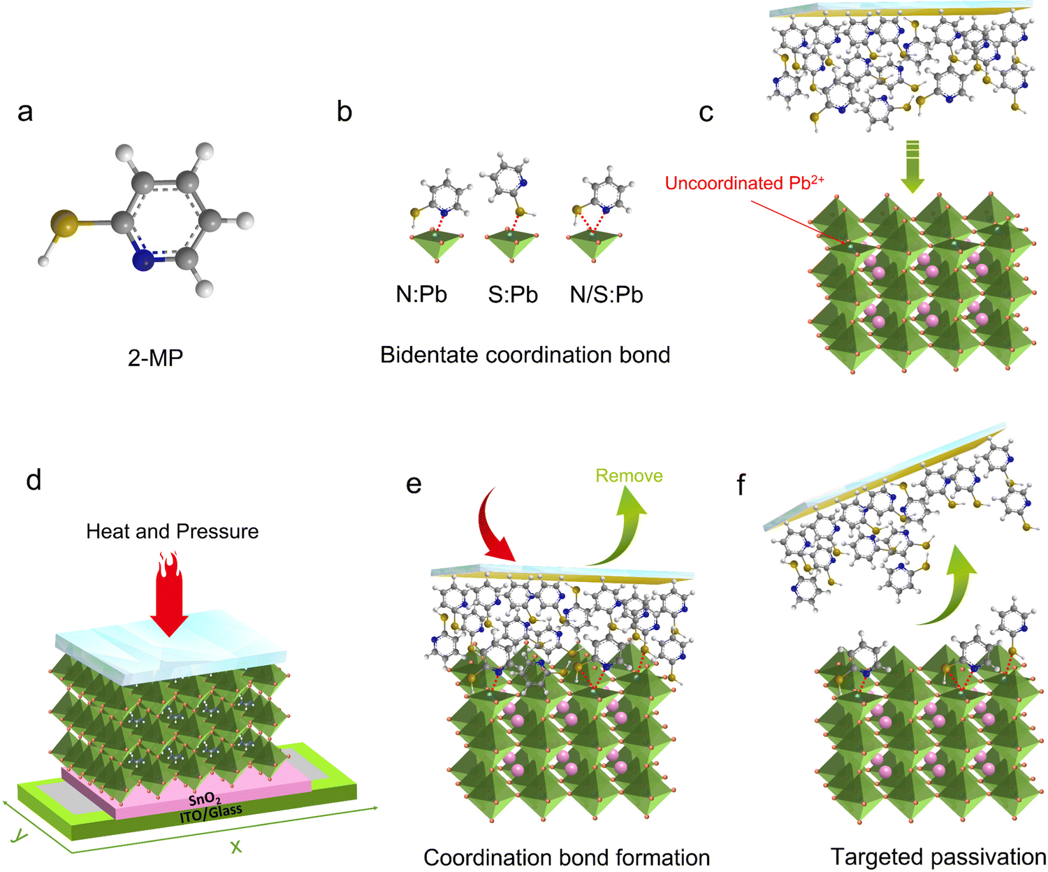 | ||
| Fig. 1 SPP process. (a) Molecular structure of 2-MP. (b) Schematic diagram of bidentate coordination bonds formed between 2-MP and perovskite. (c) Schematic diagram of uncoordinated Pb2+ defects on the perovskite surface and the pre-prepared passivator film/substrate. (d–f) Schematic diagram of the SPP process. | ||
For the SPP process, the passivator film was prepared independently in advance on a glass substrate (Methods). Subsequently, the passivator film/substrate was covered on the upper surface of the as-prepared perovskite film (Fig. 1c), with heat and pressure perpendicularly applied to make the passivator molecules closely contact and interact with the perovskite surface (Fig. 1d, the optimum temperature and pressure are 70 °C and 0.3 MPa, respectively, will be discussed in detail later). Driven by hot pressing, the passivator molecule would form coordination bonds with Pb2+ defects on the underlying perovskite surface (Fig. 1e) due to a rather strong coordination ability.36,37 After a specific treatment time, the passivator film substrate was detached, leaving the passivator molecules still anchored on the defect sites (Fig. 1f). Movie S1 (ESI†) demonstrates a real-time recording of a half-passivated and half-reference perovskite film via SPP processing, and the surfaces of the passivated and reference perovskite film look distinctly different, suggesting successful anchoring.
Mechanism and chemical interactions
The successful anchoring of passivator molecules on the surface of perovskite films is a prerequisite for surface passivation. To investigate whether the passivator molecules remain on the perovskite film surface, time-of-flight secondary-ion mass spectroscopy (ToF-SIMS) was performed on a perovskite film treated with SPP for 20 minutes (namely “SPP-20” sample). The characteristic sulfur (S) element of passivator was found to be indeed distributed on the film surface (Fig. 2a). Note that the S signal at the bottom of the film originated from the buried dimethyl sulfoxide (DMSO),38 which was also found in the untreated perovskite film (Fig. S2, ESI†). Surface S mapping of TOF-SIMS signals (Fig. 2b) also illustrated apparent signals of passivator molecules on the perovskite film surface. The reconstructed three-dimensional images based on ToF-SIMS depth profiles of different elements spatially demonstrated the surface distribution of passivator molecules in the SPP-20 sample (Fig. 2d). In addition, the emergence of the S 2p characteristic peak after SPP processing in X-ray photoelectron spectroscopy (XPS) surface elemental analysis compared to the control sample (Fig. 2c and Fig. S3a, ESI†) further confirms the successful anchoring of passivators. Moreover, Fourier transform infrared (FTIR) spectra characterization results depicted the C–S stretching vibration in the SPP-20 sample (Fig. 2e), which is the characteristic signal of the passivator molecule, thereby affirming the existence of passivator molecules.38,39 Furthermore, laser confocal Raman spectroscopy mapping was performed on the perovskite film surface at 733 cm−1 (Fig. 2f–h), and shows the characteristic stretching vibration of C–S (Fig. 2i).33 The results also revealed that the perovskite film surface exhibited stronger signals of the passivator molecule as the SPP treatment time increased. These solid pieces of evidence support that SPP can successfully anchor passivator molecules on the surface of perovskite films.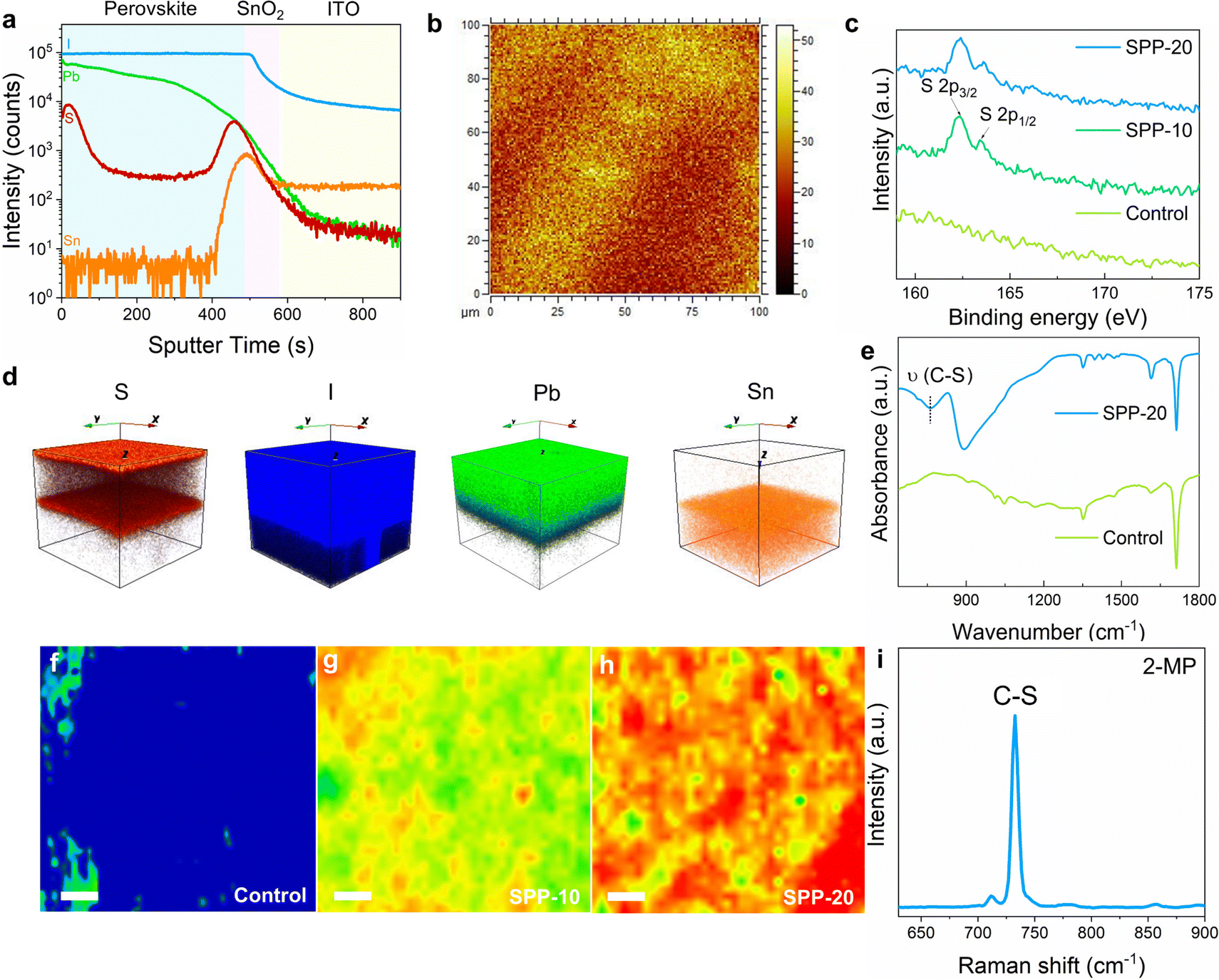 | ||
| Fig. 2 Surface distribution of the passivator after SPP processing. (a) Depth resolved ToF-SIMS of I, Pb, S, and Sn signals of the SPP-20 sample (perovskite/SnO2/ITO), where S is the characteristic element of 2-MP. (b) Surface S mapping of the SPP-20 sample based on ToF-SIMS. (c) XPS spectra of S 2p in control, SPP-10, and SPP-20 samples. (d) Reconstructed three-dimensional images of S, I, Pb, and Sn distribution in the SPP-20 sample based on ToF-SIMS depth profiles. (e) FTIR spectra of the control and SPP-20 samples. (f–h) Raman mapping image at 733 cm−1 (characteristic stretching vibrations of C–S) of control, SPP-10, and SPP-20 samples; scale bars are 5 μm. (i) Raman spectroscopy of C–S, extracted from the Raman signal of 2-MP. | ||
Further investigations on the interaction between the passivators and surface defects of perovskite films would provide insight into the SPP mechanism. The binding energy of Pb 4f of perovskite films in XPS results continuously moves to a lower value after SPP processing (Fig. 3a), which may be attributed to the formation of coordination bonds between uncoordinated lead and passivator molecules.40,41 In addition, we detected a uniform distribution of a Pb–S bond characteristic signal (205 cm−1)33,34 on the surface of the treated perovskite film by Raman micro-mapping (Fig. S4, ESI†), which confirmed the formation of chemical bonds between S atoms on the passivator molecule and Pb on the perovskite surface. Subsequently we used density functional theory (DFT) to calculate the binding energy of three possible coordination bonds (N–Pb, S–Pb, N/S–Pb) between the passivator and the perovskite. The result showed much greater strength of the three possible coordination bonds compared to the intermolecular van der Waals forces of the passivator (Fig. 3b and Fig. S5, ESI†).42–44 As a result, the passivator molecule could be peeled off from the original passivator film/substrate and anchored on the defect sites of the perovskite film surface even if the passivator film/substrate is detached (Fig. 1f). At the same time, for defect-free regions of the perovskite film surface, the passivator molecules would be removed along with the passivator film/substrate, since there is no interaction between the passivator molecules and the perovskite surface. Accordingly, the SPP process would fulfill targeted passivation: only passivating surface defects, and not affecting the benign regions without defects. This would not leave an unnecessary passivator on the film surface, which is one of the most attractive features of solid-phase passivation.
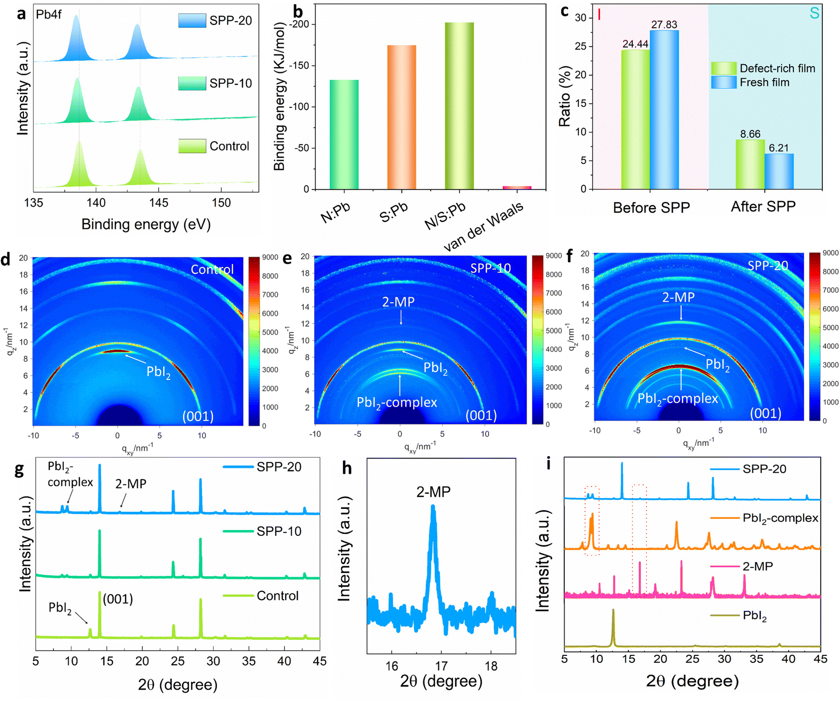 | ||
| Fig. 3 Mechanism and chemical interactions between the passivator and the perovskite in the SPP process. (a) The XPS spectra of Pb 4f of the control, SPP-10 and SPP-20 films. (b) Calculated binding energies of the three coordination bonds (N:Pb, S:Pb, N/S:Pb) and strength comparison with van der Waals force. (c) Content proportion of I and S in XPS mapping of aged and fresh perovskite films before and after SPP. (d–f) The GIWAXS results of control, SPP-10 and SPP-20 films. (g) XRD results of control, SPP-10 and SPP-20 films. (h) The zoomed-in part of the 2-MP peak of the SPP-20 film in (g). (i) The XRD characterization of PbI2, 2-MP, PbI2-complex and SPP-20 samples. | ||
In order to prove targeted passivation, we deliberately designed an experiment to make a comparison between a defect-rich perovskite film and a reference film after SPP, since more passivator molecules should be found on the defect-rich perovskite surface in targeted passivation. In order to obtain a defect-rich perovskite film, we stripped off the gold (Au) electrode and washed off the Spiro-OMeTAD of the PSC after aging for 800 hours at MPP tracking (Fig. S6, ESI†), since the operation of PSC will lead to the loss of I− through ion migration and generation of I2, thus creating more uncoordinated Pb2+ defects on the perovskite surface (discussed later). XPS elemental mapping (Fig. S7, ESI†) indicated that the defect-rich perovskite film aged by MPP tracking possesses a lower proportion of the I signal at the surface (24.44%) than the fresh perovskite film (27.83%) (Fig. 3c), indicating more I vacancy and uncoordinated Pb2+ defects. The aged perovskite film has more defects than the fresh perovskite film was confirmed by time-resolved photoluminescence (TRPL) lifetime results (Fig. S8, ESI†). After SPP processing, a higher content of S signal was found on the defect-rich film (8.66%) compared to the fresh film (6.21%) (Fig. 3c), suggesting that more passivator molecules were anchored on the surface of the defect-rich perovskite film. This result strongly implies that SPP is a targeted passivation process. This targeted passivation was further confirmed by the designed half-passivation experiment (Note S2, ESI†).
We found the diffraction peak of the passivator (2-MP, 2θ = 16.8°) in the SPP-20 sample from X-ray diffraction (XRD) results (Fig. 3g–i). The synchrotron-radiation-based grazing-incidence wide-angle X-ray scattering (GIWAXS) also showed a gradual stronger characteristic signal of 2-MP in the SPP-10 and SPP-20 samples (Fig. 3d–f and Fig. S11–S13, ESI†). Due to the strong coordination ability of passivator molecules to Pb2+, we found that PbI2 distributed at the surface grain boundary (GB) of the perovskite film was transformed into a PbI2-complex in situ by interacting with the anchored passivator during the SPP process (Fig. 3g–i and Fig. S14–S17, ESI†). SEM results showed that white PbI2 obviously disappeared (Fig. S14, ESI†). In addition, the comparison experiments also confirmed that the changes in morphology were not caused by temperature or pressure (Fig. S15, ESI†). After transforming PbI2 at GB into the PbI2-complex, we found that the I-type band alignment could be formed according to UV absorption and ultraviolet photoelectron spectroscopy (UPS) characterization results (Fig. S18, ESI†), which has been proved to be an efficient passivation strategy to reduce the non-radiative recombination loss of carriers at GB.45 Moreover, the photodegradation of PbI2 has been recognized as an unresolved problem to deteriorate the stability of PSCs in the perovskite community,46,47 converting PbI2 into the PbI2-complex could effectively alleviate the notorious photodegradation of PbI2 (discussed later). We also demonstrated that solid-phase passivation can work efficiently even without excessive PbI2 in the original perovskite film (Fig. S19, ESI†).
Enhanced optoelectronic properties
Subsequently, we used DFT to calculate the density of states (DOS) of perovskite before and after SPP treatment under three possible coordination bond conditions (Fig. 4a). The results illustrated that the uncoordinated Pb2+ on the surface of the control perovskite will introduce a deep trap state in the band gap (∼0.5 eV), and could capture carriers as non-radiative recombination centers.48,49 In contrast, these deep trap states could be effectively suppressed after SPP processing by any of the three possible bonding conditions (Fig. 4a). The calculated results are consistent with the remarkable reduction of nonradiative recombination observed by a fourfold increase (from 168 to 684 ns) of the TRPL lifetime (Fig. 4b), a more than threefold enhancement of the photoluminescence intensity (Fig. S20a and d–f, ESI†) and photoluminescence quantum yield (PLQY) (Table S1, ESI†), which objectively reflect the defect density on the perovskite films.50–52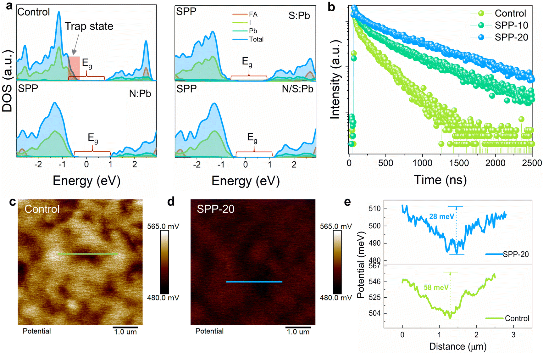 | ||
| Fig. 4 Optoelectronic property characterization. (a) DOS of the control perovskite with uncoordinated Pb2+ defects and passivated perovskite via three bonding methods, and the band gap range is marked with red brackets. (b) TRPL results of control, SPP-10 and SPP-20 samples, and the fitted lifetimes are 168, 328 and 684 ns, respectively. (c and d) The surface potential mapping of control and SPP-20 perovskite films from KPFM measurements, and the white line is the path for quantitative measurement of potential. (e) Potential difference between grain boundary and grain interior of line scanning. | ||
Kelvin probe force microscopy (KPFM) was conducted to further probe the effect of SPP on the surface properties of perovskite films. The results displayed that SPP reduced the potential difference between GB and the surface of grain interiors to about half of the control sample (Fig. 4c–e), delivering a more uniform surface potential distribution for better carrier interface extraction.53 The reduced potential difference in the SPP sample is mainly due to the lower potential at the grain surface compared to the control sample, which further suggests that passivator molecules are located at the grain surface and chemically interact with the perovskite lattice. The relatively lower surface potential caused by passivator molecules could be attributed to the downward-shifted Fermi level and more p-type conductivity in the SPP sample.54–56 UPS characterization further verified the upward-bending energy band on the surface of the SPP film (Fig. S21, ESI†), enabling better interfacial transport of carriers.57 Picosecond transient absorption (ps-TA) spectroscopy was performed to examine the carrier interface transport dynamics between the perovskite and the hole transport layer (Fig. S22, ESI†). The result proved that the SPP sample did exhibit faster decay due to better carrier transport at the interface (Fig. S21f, ESI†).58,59 Improving the interface transport of carriers will also reduce the accumulation of carriers at the interface, which can effectively reduce the carrier recombination loss to improve the VOC.57
The enhanced optoelectronic properties of the perovskite films encouraged us to investigate the favorable effects of SPP at the device level. The SPP-20 device features an order of magnitude lower dark current in current density–voltage (J–V) characterization (Fig. S23, ESI†), reflecting the suppressed charge-carrier recombination.60 The fitted recombination resistance via electrochemical impedance spectroscopy dramatically enhanced from 2146 to 3938 Ω after SPP treatment (Fig. S24a, ESI†), signifying an effective suppression of carrier recombination. In addition, the lifetime extracted from the transient photovoltage (TPV) measurement in real PSCs was doubled from 2010 to 4030 ns after SPP treatment (Fig. S24b, ESI†), indicative of the effective suppression of carrier recombination in SPP-based PSCs. It should be noted that TPV is only a horizontal comparison between the control and SPP samples, because the same electrode capacitance exists in the control and SPP samples which is difficult to be eliminated, and the measured values do not represent the real lifetimes of charge carriers in the perovskite.61–63
Enhanced photovoltaic performance
We then fabricated perovskite solar cell devices (Glass/ITO/SnO2/Perovskite/Spiro-OMeTAD/Au) (Fig. 5a) using SPP to investigate their photovoltaic performance. The cross-sectional SEM (Fig. 5b) and CLSM images (Fig. 5c) of PSC showed super high film quality and a columnar character for the crystal grains from the bottom to the top with a film thickness of ∼800 nm. The control PSC possesses a PCE of 22.37% under reverse scanning, with a short circuit current density (JSC) of 25.20 mA cm−2, an open circuit voltage (VOC) of 1.10 V and a FF of 0.807 (Fig. 5d). Fig. 5e shows significantly elevated efficiency in one of our best SPP-based PSCs, with a reverse scan PCE of 25.20% (JSC: 25.23 mA cm−2, VOC: 1.194 V and FF: 0.837). This device also exhibited negligible hysteresis under both forward and reverse scans between −0.01 and 1.21 V. We found that the VOC reached 1.2 V in another SPP-PSC, delivering an ultra-small voltage loss of 0.34 V (Fig. S26, ESI†), representing ∼96% of the thermodynamic limit.13 The stabilized power output at MPP is 21.40% and 24.68% for control and SPP-PSCs, respectively (Fig. 5f). The certified PCE is 24.65%, with a high VOC of 1.192 V (Fig. S27, ESI†). After two months of storage, the PSC was sent to National PV Industry Measurement and Testing Center for the second efficiency certification, and a rather high PCE of 24.29% was obtained (Fig. S28, ESI†). These results highlight the superiority of SPP in improving the photovoltaic performance of PSCs. The statistical distribution of PCE of 32 individual devices indicated reliable reproducibility of photovoltaic performance improvement (Fig. 5g). The markedly increased VOC (average VOC: from 1.097 to 1.182 V) and FF (average FF: from 0.793 to 0.820) are responsible for the soaring PCE (average PCE: from 21.92% to 24.42%, Fig. 5g and Fig. S29, ESI†), due to substantially suppressed non-radiative recombination and better carrier transport.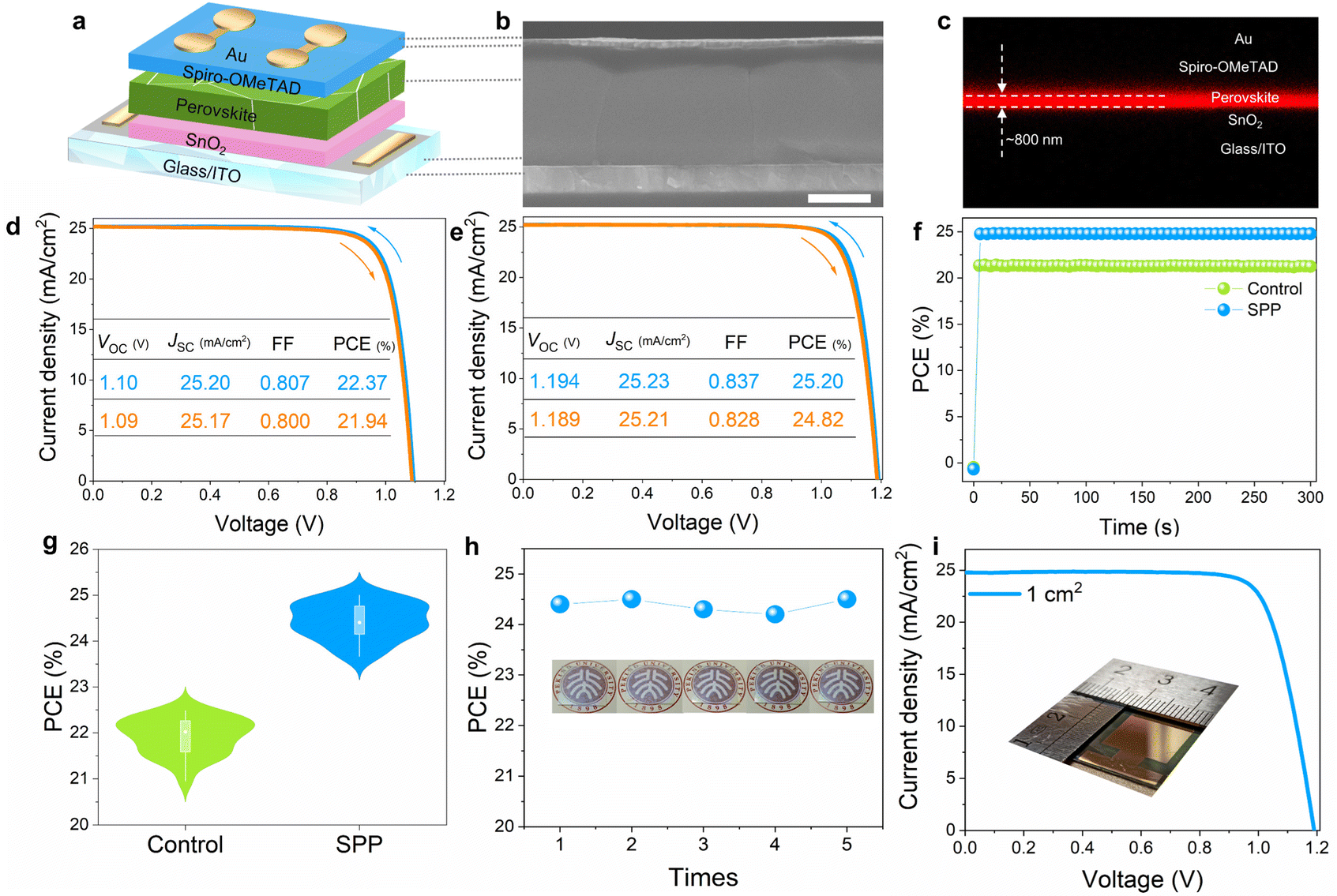 | ||
| Fig. 5 Photovoltaic performance characterization. (a) Structure of a PSC. (b) The cross-sectional SEM image of the SPP-PSC, scale bar is 500 nm. (c) The cross-sectional CLSM image of the fabricated SPP-PSC. (d) The J–V curves of the control PSC under reverse and forward scans. (e) The J–V curves of SPP-20 PSC under reverse and forward scans. (f) SPO of the control and SPP devices at MPP. (g) The statistical distributions of PCE of the control and SPP-20 PSCs. (h) PCE of PSCs treated by the repeatedly used passivator film, the inset shows the photos of the passivator film after each use. (i) The J–V curves of SPP-20 PSC under reverse scan with an area of 1 cm2, the inset is a photo of a large area PSC. | ||
More importantly, the passivator film was found reusable many times without affecting the photovoltaic performance enhancement of PSCs. Fig. 5h shows the PCE of five PSCs treated by the same passivator film and the photos of the passivator film after each use (detailed photovoltaic parameters are summarized in Table S2, ESI†). Both the PCE boost and the morphology of the passivator remained almost identical after five times of usage. This technology is highly attractive for industrial low-cost mass production and is also reported in the perovskite community for the first time. Moreover, in our solid-phase passivation, passivator films and perovskite films are prepared independently and the final passivation effect is less dependent on the passivator film quality. Therefore, passivator films can be prepared by various methods, not just spin coating (Fig. S30, ESI†), giving SPP an attractive potential for size compatibility. For example, we show that the SPP-based PSC with an area of 1 cm2 exhibits a rather high PCE of 23.05% under reverse scan with a JSC of 24.90 mA cm−2, VOC of 1.19 V and FF of 0.778 (Fig. 5i and Fig. S31, ESI†), endowing the SPP strategy with great potential for industrial scale-up applications. Statistical analysis of the photovoltaic parameters of SPP 1 cm2 PSCs demonstrates a greatly increased VOC and PCE compared to the control devices (Fig. S31, ESI†).
In addition, the effect of temperature on SPP was investigated and 70 °C was found to be appropriate for better device performance (Fig. S32, ESI†). The pressure is only used to make the passivator film and perovskite film contact closely to achieve uniform passivation, so the required pressure is relatively small. We found that the pressure of 0.3 MPa is the minimum critical pressure for close contact between the passivator film and the perovskite film, and higher pressures did not contribute more to the device performance (Fig. S33, ESI†). In addition, we also confirmed that the significantly improved photovoltaic performance is not due to temperature or pressure during the SPP process (Fig. S15, ESI†). Another effective passivation agent was also applied to solid phase passivation (Fig. S34, ESI†) and was found also effective in enhancing the photovoltaic performance of PSCs. We also compared the photovoltaic performance of PSCs via the SPP method and conventional solution method by spin-coating the same passivator on the perovskite surface (Methods, Fig. S35, S36 and Table S3, ESI†).33 It can be found that solid phase passivation can indeed passivate the defects of perovskite film better, and statistical analysis of the photovoltaic parameters of SPP-PSCs demonstrates that enhanced FF and VOC mainly contribute to a higher PCE. The solid-phase method can better improve the photovoltaic performance of perovskite solar cells due to several possible reasons: targeted passivation without the passivator residue; no surface component damage by solvent dissolution; no solution penetration downward, as summarized in Note S1 and Fig. S1 (ESI†).
Finally, we move our investigation to stability characterization. We found that SPP processing can notably increase the water contact angle of perovskite films (Fig. S37, ESI†), thus improving their moisture resistance for better stability. We then examined the degradation of SPP and control perovskite films in a high humidity environment (Fig. S38a, ESI†) and the control sample is easier to turn yellow than the SPP sample (Fig. S38b, ESI†). In addition, how to take advantage of the self-passivation of PbI2 while avoiding its photo-instability is still a difficult problem in the community. We tested the photostability of PbI2 and the PbI2-complex by soaking them under 1 Sun illumination, and found much better photostability of the PbI2-complex compared to pure PbI2 by showing an almost unchanged XRD peak during light soaking for 18 hours (Fig. S39, ESI†). Therefore, the anchoring of passivator molecules at the GB can not only achieve GB passivation function, but also effectively avoid the notorious photodegradation of PbI2, providing an insightful view toward solving the double-edged sword effect of PbI2 in perovskite photovoltaics. On the other side, it has been reported that iodine generated during operation will act as a defect to further weaken both the efficiency and stability of PSCs.38,64 Here, we found that the delicately selected passivator molecules can well reduce the I2 back to I−. UV-visible absorption spectra characterization confirmed that I2 was almost completely reduced after adding a passivator to the I2 solution (Fig. 6a), which can also be visually observed in Fig. 6b. To further evaluate its effect on perovskite films, we soaked the control and SPP-20 perovskite films in toluene and illuminated them under AM 1.5G irradiation for 48 hours. The UV-visible absorption spectra of the obtained toluene solutions strongly suggest that the generation of iodine found in the control sample has been completely suppressed in the SPP-20 sample (Fig. S40, ESI†), which is of great significance to improve the operation stability of the PSCs. Thermal stability is a challenge that must be faced during device operation, and we thus carried out the thermal stability characterization of the control and SPP-treated perovskite films (Fig. S41, ESI†), which reveals that the SPP-20 perovskite film also shows better thermal stability.
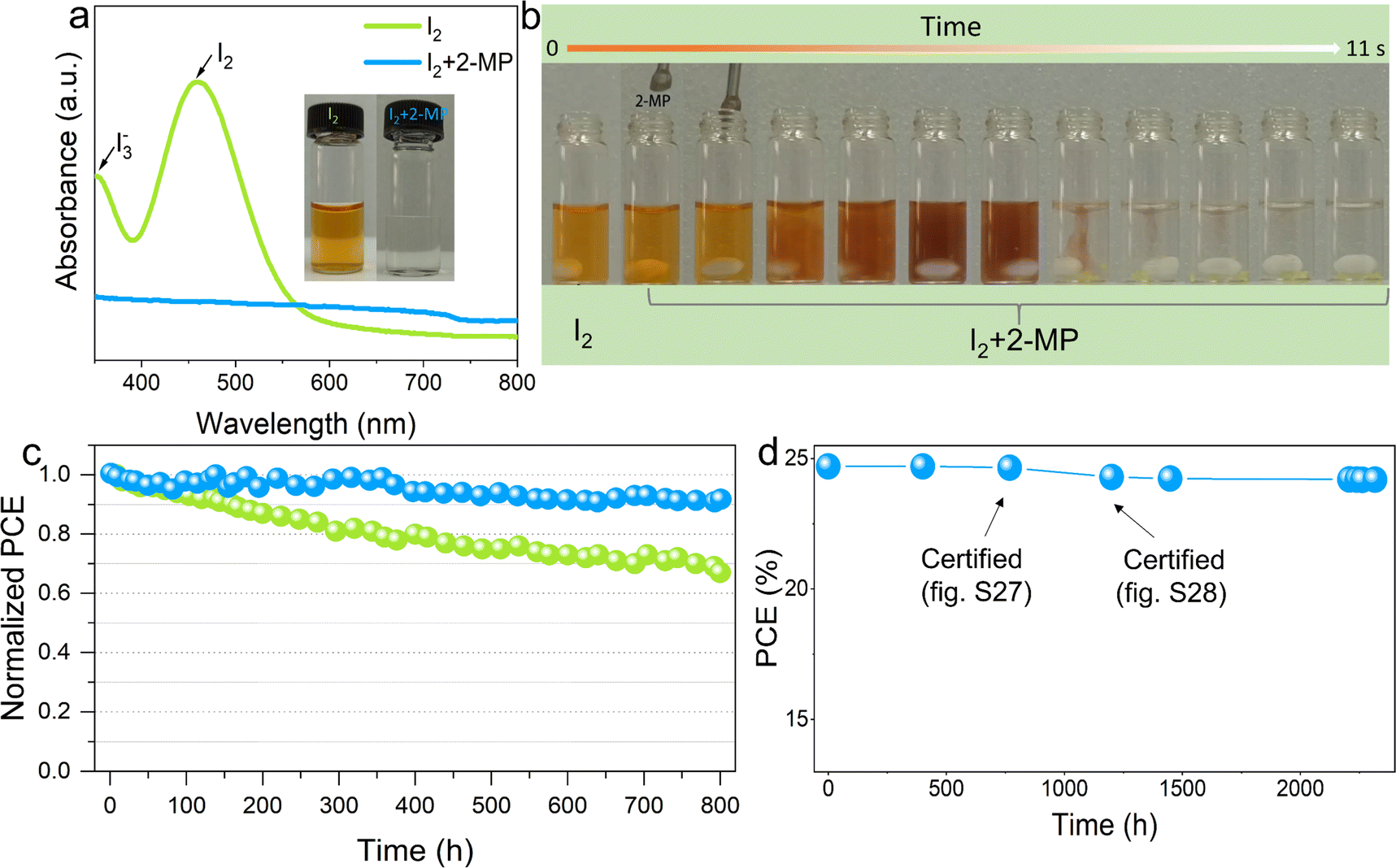 | ||
| Fig. 6 Stability characterization. (a) UV absorption spectrum of I2 in deionized water before and after the addition of 2-MP; the insets show their corresponding pictures. (b) The process of 2-MP reduces the I2 back to I− during stirring after adding 2-MP into the I2 solution. (c) The operational stability test based on the unencapsulated PSCs. Blue and green represent SPP and control PSC, respectively. (d) Storage stability test based on the unencapsulated PSCs in nitrogen. | ||
Then we examined the operational stability of SPP solar cell devices under continuous 1 Sun (AM 1.5G) illumination and MPP tracking in nitrogen at 40 °C. The unencapsulated SPP device (JSC: 25.20 mA cm−2, VOC: 1.18 V, FF: 0.815 and PCE: 24.23%) maintained over 92% of its initial PCE after 800 hours (Fig. 6c). Moreover, the unencapsulated SPP device maintains 98% of its original efficiency after being stored under nitrogen for more than 2300 hours (Fig. 6d). The results highlight the significant advantages of SPP in improving the stability of PSCs due to several reasons: greatly reduced defect density on the surface of the perovskite films, increased water contact angle of the perovskite films, enhanced photostability of PbI2 at grain boundaries and efficient reduction of I2 generated during operation.
Conclusions
In summary, we have proposed a solvent-free solid-phase passivation strategy to efficiently bond uncoordinated Pb2+ defects on the surface of perovskite films, and largely reduce the non-radiative recombination loss of carriers. As a result, the SPP processed PSCs have achieved a high VOC of up to 1.2 V (voltage loss of only 0.34 V), and a remarkably improved PCE from 22.37% to a certified 24.65%. The SPP process enables unique targeted passivation in principle: passivating surface defect sites without affecting defect-free benign regions of the perovskite surface. In addition, the solid-phase strategy possesses many unique merits over the solution method. For example, the solid-phase method holds great potential being compatible with large-area PSCs for future industrial production since passivator films with required sizes can be independently prepared in advance. Furthermore, SPP passivator films can be fabricated by various techniques, which breaks the constraint of passivator selection in the solution method, thereby providing more possibilities for exploring more effective passivators.Experimental section
Materials
The SnO2 colloid precursor was purchased from Alfa Aesar (Tin(IV) oxide, 15% in H2O colloidal dispersion). PbI2 (super-dry beads, 99.999%), CsCl (super-dry beads, 99.999%), N,N-dimethylformamide (DMF, 99.8%), dimethyl sulfoxide (DMSO, 99.9%), acetonitrile (ACN, 99.9%), isopropyl alcohol (IPA, 99.7%), and chlorobenzene (CB) were purchased from Sigma-Aldrich. Lithium bis(trifluoromethanesulfonyl)imide (Li-TFSI, 98%), 4-tert-butylpyridine (4-TBP, 96%), formamidinium iodide (FAI), methylammonium chloride (MACl), phenethylammonium iodide (PEAI), butylammonium iodide (BAI), and 2,2′,7,7′-tetrakis(N,N-p-dimethoxy-phenylamino)-9,9′-spirobifluorene (Spiro-OMeTAD, 99.8%) were purchased from Xi’an Polymer Light Technology Corporation. 2-Mercaptopyridine (2-MP), pyridine (Py) and p-toluenethiol (PTT) were purchased from Tokyo Chemical Industry. All the chemicals were used as received without further purification.Materials and solar cell device fabrication
Highly transparent glass/ITO (≈15 Ω sq−1) was scrubbed vigorously with a dust-free cloth and cleaners, and then they were cleaned with an ultrasonic cleaner for 40 minutes using deionized water, acetone and IPA sequentially. Before use, the ITO-coated glass was dried with a nitrogen gun and treated with 90 W plasma for 60 seconds to improve its wettability. Then, SnO2 solution (3.75%, diluted with deionized water) was spin-coated on ITO at 3000 rpm for 30 s and annealed in ambient air at 150 °C for 30 min. PbI2 (691.5 mg) and CsCl (12.6 mg) in DMF: DMSO = 900 mL: 100 mL were stirred for an hour and filtered with a 0.22 μm PTFE filter. After the films were cooled down to room temperature, 60 μL of PbI2 solution was spin-coated on SnO2 at 1500 rpm for 30 s and then annealed at 70 °C for 1 min. Subsequently, 100 μL of filtered organic salt solution containing FAI: MACl (90 mg: 9 mg in 1 mL of IPA) was spin-coated on room-temperature PbI2 films at 2000 rpm for 30 s using a pipette with a trimmer head. The spin coater needs to be rotated immediately once the organic salt solution is dripped onto the PbI2 films. Then, the films should be transferred from the glove box to a hot plate in the atmosphere (30–40% humidity) for annealing at 150 °C for 15 min.65 It should be noted that both the PbI2 and organic salt solutions need to be fresh. For SPP, (1) preparing the passivator precursor: 18 mg of 2-MP powder was dissolved in 1 mL of IPA and stirred for an hour at room temperature. Then, the passivator precursor solution was filtered with a 0.22 μm PTFE filter. Since the concentration of the passivator precursor only affects the thickness of the solid phase passivator film, and SPP only needs the passivator molecules on the surface of the passivator film, and thus the thickness of the solid passivator film or the concentration of the passivator precursor has no remarkable effect on the experimental results. (2) Preparing a solid phase passivator film/substrate: The cleaned glass substrates were treated with 90 W plasma for 120 seconds, and then the 2-MP precursor solution was spin-coated on the glass substrates at 1500 rpm for 30 s and then annealed at 70 °C for 3 min. (3) For the SPP process, the hot plate needs to be preheated to 70 °C. Then, the prepared passivator film/substrate was carefully covered on the perovskite film, and then 0.3 MPa pressure was applied vertically on the passivator film/substrate at 70 °C. External forces applied vertically should not cause friction between the two films, which could cause serious damage to the perovskite film. After 20 minutes, the passivator film/substrate was removed vertically and carefully. Then, mixed Spiro-OMeTAD solution, prepared by mixing 72.3 mg of spiro-OMeTAD in 1 mL of chlorobenzene, 28.8 μL of 4-tertbutylpyridine solution, and 17.5 μL of LiTFSI solution (520 mg mL−1 in acetonitrile), respectively, was spin-cast on the surface of the perovskite films at 4000 rpm for 30 s. After that, the films need to be oxidized for 12 hours in a drying cabinet with a relative humidity of 1%. Finally, a gold electrode was thermally evaporated with a thickness of about 90 nm at a low vacuum of 8 × 10⁻⁵ Pa. The evaporation speed was 0.01 nm s−1 for the first 15 nm and 0.03 nm s−1 for the rest of the procedure. Then, the PSCs should be oxidized for 36 hours in a drying cabinet with a relative humidity of 1% before characterization. For surface passivation by the solution method, 2-MP (13.5 mM) in chlorobenzene solution was spin coated onto the perovskite films at 1000 rpm for 30 s followed by 6000 rpm for 5 s.33 For the preparation of the PbI2-complex, 2-MP solution (1.8 M in DMF) and PbI2 solution (0.6 M in DMF) were mixed and stirred at room temperature for five minutes. Then, the precipitate could be obtained by pouring the mixed solution into a large amount of toluene. The precipitate should be washed with toluene many times and vacuum drying at room temperature for 8 hours.Perovskite film characterization
The crystal structure and phase composition were determined with an X'Pert Pro (Holland) X-ray diffractometer with Cu Kα1 radiation (λ = 0.154 nm). XPS spectra were recorded at a base pressure of 1.0 × 10⁻⁹ Torr using a monochromatic Al-Kα X-ray source. The surface electronic states were investigated by ultraviolet photoelectron spectroscopy (UPS, Axis Ultra, Kratos Analytical Ltd) and non-monochromated He Iα (hν = 21.22 eV) was used as the photon source. UV absorption spectra were recorded using a UV-2500 (Shimadzu Corporation). The absorption spectra of the perovskite layers were measured by UV-vis spectrometry using a UV-2600 (Shimadzu). The PL and TRPL were investigated at room temperature using an FLS980 (Edinburgh Instruments) spectrometer with a 450 W Xenon lamp. When TRPL characterization was carried out, the films were excited at 520 nm with a repetition rate of 200 kHz and a fluence of 34 nJ cm−2 per pulse. CLSM characterization was performed on a homemade Olympus FV3000 CLSM system with a 100× objective lens. The surface and cross-sectional morphology of the perovskite films and device were recorded using an SEM (Quanta FEG 450) under 10 kV electron beam accelerating voltage. Grazing Incidence Wide Angle X-ray Scattering (GIWAXS) measurements were performed at the BL14B1 beamline, Shanghai Synchrotron Radiation Facility (SSRF). The wavelength of the X-rays was 1.24 Å (10 KeV) and varying incidence angles were adopted together with an exposure time of 30 s. The diffraction patterns were collected using a two-dimensional Mar225 detector. TOF-SIMS was performed at an energy of 1 keV and a current of 200 nA, and the detected area was 300 × 300 μm.Device characterization
The J–V curves were performed in the atmosphere using an Agilent B2900 series precision source/measure unit with a scanning rate of 50 mV s−1 (a voltage step of 10 mV and a delay time of 200 ms) from 1.21 to −0.01 V (reverse) or from −0.01 to 1.21 V (forward). The cells were illuminated with a Xeon lamp solar simulator (Solar IV-150A, Zolix) under AM 1.5G irradiation (100 mW cm−2), which was calibrated using a Newport calibrated KG5-filtered Si reference cell. EQE and absorption spectra measurements were performed on a solar cell QE/IPCE measurement system (Solar Cell Scan100, Zolix), which was calibrated with a certified silicon solar cell. The scan interval was 1 nm and there was no bias light used during the measurement. An operational stability test was performed using an AM 1.5G white-LED solar simulator and by setting the bias voltage to the initial MPP and tracing the current density. TPV measurement was carried out on a homemade system. To calculate the photocurrent density, we define the area using an aperture (0.0478 cm2) placed on the glass side of the device to avoid overestimation of the photocurrent density. The cells were unencapsulated during all tests. The impedance spectrum was recorded using a potentiostat electrochemical workstation (AUT50690, PGSTAT204, the Netherlands) at different biases and the frequency ranges from 1 MHz to 0.01 Hz with 100 data points.Computational methods
The structural and electronic properties of perovskite surfaces were investigated using first-principles calculations based on density functional theory (DFT) as implemented in the Vienna ab initio simulation package (VASP). Interactions between ions and electrons were treated by the frozen-core projector augmented-wave (PAW) method. The Perdew–Burke–Ernzerhof (PBE) implementation of the generalized gradient approximation (GGA) was employed as exchange-correlation potentials. A kinetic energy cutoff of 400 eV was chosen for the plane-wave basis set. The Brillouin zone was sampled using a Monkhorst-Pack k-point grid with a resolution of 0.2 Å−1. A vacuum space of 20 Å along the z-axis was adopted to prevent image interaction. Dipole corrections (IDIPOL = 3) were considered to correct the polar effect of the surface. Grimme's DFT-D3 correction utilizing the Becke–Johnson damping scheme was applied to account for the van der Waals interactions. During the relaxation, the bottom layers were fixed at the bulk crystal geometry. Geometries were optimized until the energy was converged to 1.0 × 10⁻⁶ eV and the force was converged to 0.005 eV Å−1.The binding energy (Ebinding) is defined as
| Ebinding = Esurface + Epassivator − Etotal, |
Author contributions
Q. Z. and C. L. conceived the idea and designed the experiments. C. L. and X. J. W. contributed to the fabrication of PSCs. G. H. J. Z. and X. Y. G. provided the GIWAXS characterization and analysis. X. J. W. performed the SEM characterization and film microstructure analysis. F. G. synthesized the relevant chemicals and performed the MPP tracking characterization. C. L., X. J. W., F. G. and C. L. Z. contributed to the J–V and EQE measurements. Q. Z. supervised the whole project. Q. Z. and C. L. co-wrote the paper. All authors were involved in the characterization of films and the discussion of data analysis.Conflicts of interest
There are no conflicts to declare.Acknowledgements
We thank BL14B1 in the Shanghai Synchrotron Radiation Facility for providing the beam time. We also sincerely thank Dr Yiming Li and Prof. Qingbo Meng from the Institute of Physics, CAS, for their generous assistance with TPV measurements. This work was supported by the National Key Research and Development Program of China (No. 2019YFE0114100 and 2019YFA0707003), the National Natural Science Foundation of China (NSFC 52272178 and 51872007), the Beijing Municipal Natural Science Foundation (No. 7202094) and the Peking University BHP Billiton “Carbon and Climate” Wei-Ming Scholars Program (WM202201).References
- S. Bai, P. M. Da, C. Li, Z. P. Wang, Z. C. Yuan, F. Fu, M. Kawecki, X. J. Liu, N. Sakai, J. T. W. Wang, S. Huettner, S. Buecheler, M. Fahlman, F. Gao and H. J. Snaith, Nature, 2019, 571, 245 CrossRef CAS PubMed.
- Y. C. Zhao, T. Heumueller, J. Y. Zhang, J. S. Luo, O. Kasian, S. Langner, C. Kupfer, B. W. Liu, Y. Zhong, J. Elia, A. Osvet, J. C. Wu, C. Liu, Z. Q. Wan, C. Y. Jia, N. Li, J. Hauch and C. J. Brabec, Nat. Energy, 2021, 7, 144 CrossRef.
- Z. L. Guo, A. K. Jena, G. M. Kim and T. Miyasaka, Energy Environ. Sci., 2022, 15, 3171–3222 RSC.
- Y. Choi, D. Koo, G. Jeong, U. Kim, H. Kim, F. Z. Huang and H. Park, Energy Environ. Sci., 2022, 15, 3369–3378 RSC.
- J. J. Xue, R. Wang, X. H. Chen, C. L. Yao, X. Y. Jin, K. L. Wang, W. C. Huang, T. Y. Huang, Y. P. Zhao, Y. X. Zhai, D. Meng, S. Tan, R. Z. Liu, Z. K. Wang, C. H. Zhu, K. Zhu, M. C. Beard, Y. F. Yan and Y. Yang, Science, 2021, 371, 636 CrossRef CAS PubMed.
- W. Hui, L. F. Chao, H. Lu, F. Xia, Q. Wei, Z. H. Su, T. T. Niu, L. Tao, B. Du, D. L. Li, Y. Wang, H. Dong, S. W. Zuo, B. X. Li, W. Shi, X. Q. Ran, P. Li, H. Zhang, Z. B. Wu, C. X. Ran, L. Song, G. C. Xing, X. Y. Gao, J. Zhang, Y. D. Xia, Y. H. Chen and W. Huang, Science, 2021, 371, 1359 CrossRef CAS PubMed.
- E. B. Bi, W. T. Tang, H. Chen, Y. B. Wang, J. Barbaud, T. H. Wu, W. Y. Kong, P. Tu, H. Zhu, X. Q. Zeng, J. J. He, S. Kan, X. D. Yang, M. Gratzel and L. Y. Han, Joule, 2019, 3, 2748–2760 CrossRef CAS.
- C. Luo, W. Li, J. Fu and W. Q. Yang, Chem. Mater., 2019, 31, 5616–5624 CrossRef CAS.
- J. B. Chen, Y. G. Yang, H. Dong, J. R. Li, X. Y. Zhu, J. Xu, F. Pan, F. Yuan, J. F. Dai, B. Jiao, X. Hou, A. K. Y. Jen and Z. X. Wu, Sci. Adv., 2022, 8, 2722 CrossRef PubMed.
- S. Sanchez, S. Cacovich, G. Vidon, J. F. Guillemoles, F. Eickemeyer, S. M. Zakeeruddin, J. E. K. Schawe, J. F. Loffler, C. Cayron, P. Schouwink and M. Graetzel, Energy Environ. Sci., 2022, 15, 3862–3876 RSC.
- Q. Cao, J. B. Yang, T. Wang, Y. K. Li, X. Y. Pu, J. S. Zhao, Y. X. Zhang, H. Zhou, X. Q. Li and X. H. Li, Energy Environ. Sci., 2021, 14, 5406–5415 RSC.
- C. Luo, G. Zheng, F. Gao, X. Wang, Y. Zhao, X. Gao and Q. Zhao, Joule, 2022, 6, 240–257 CrossRef CAS.
- R. Azmi, E. Ugur, A. Seitkhan, F. Aljamaan, A. S. Subbiah, J. Liu, G. T. Harrison, M. I. Nugraha, M. K. Eswaran, M. Babics, Y. Chen, F. Xu, T. G. Allen, A. U. Rehman, C.-L. Wang, T. D. Anthopoulos, U. Schwingenschlögl, M. D. Bastiani, E. Aydin and S. D. Wolf, Science, 2022, 376, 73–77 CrossRef CAS PubMed.
- J. Siekmann, S. Ravishankar and T. Kirchartz, ACS Energy Lett., 2021, 6, 3244–3251 CrossRef CAS.
- Z. Y. Ni, C. X. Bao, Y. Liu, Q. Jiang, W. Q. Wu, S. S. Chen, X. Z. Dai, B. Chen, B. Hartweg, Z. S. Yu, Z. Holman and J. S. Huang, Science, 2020, 367, 1352 CrossRef CAS PubMed.
- X. P. Zheng, Y. Hou, C. X. Bao, J. Yin, F. L. Yuan, Z. R. Huang, K. P. Song, J. K. Liu, J. Troughton, N. Gasparini, C. Zhou, Y. B. Lin, D. J. Xue, B. Chen, A. K. Johnston, N. Wei, M. N. Hedhili, M. Y. Wei, A. Y. Alsalloum, P. Maity, B. Turedi, C. Yang, D. Baran, T. D. Anthopoulos, Y. Han, Z. H. Lu, O. F. Mohammed, F. Gao, E. H. Sargent and O. M. Bakr, Nat. Energy, 2020, 5, 131–140 CrossRef CAS.
- H. Z. Lu, Y. H. Liu, P. Ahlawat, A. Mishra, W. R. Tress, F. T. Eickemeyer, Y. G. Yang, F. Fu, Z. W. Wang, C. E. Avalos, B. I. Carlsen, A. Agarwalla, X. Zhang, X. G. Li, Y. Q. Zhan, S. M. Zakeeruddin, L. Emsley, U. Rothlisberger, L. R. Zheng, A. Hagfeldt and M. Gratzel, Science, 2020, 370, 74 CrossRef PubMed.
- A. B. Yusoff, M. Vasilopoulou, D. G. Georgiadou, L. C. Palilis, A. Abate and M. K. Nazeeruddin, Energy Environ. Sci., 2021, 14, 2906–2953 RSC.
- A. F. Castro-Mendez, J. Hidalgo and J. P. Correa-Baena, Adv. Energy Mater., 2019, 9, 1901489 CrossRef CAS.
- Q. Wang, B. Chen, Y. Liu, Y. H. Deng, Y. Bai, Q. F. Dong and J. S. Huang, Energy Environ. Sci., 2017, 10, 516–522 RSC.
- J. J. Yoo, G. Seo, M. R. Chua, T. G. Park, Y. L. Lu, F. Rotermund, Y. K. Kim, C. S. Moon, N. J. Jeon, J. P. Correa-Baena, V. Bulovic, S. S. Shin, M. G. Bawendi and J. Seo, Nature, 2021, 590, 587–593 CrossRef CAS.
- X. P. Zheng, B. Chen, J. Dai, Y. J. Fang, Y. Bai, Y. Z. Lin, H. T. Wei, X. C. Zeng and J. S. Huang, Nat. Energy, 2017, 2, 17102 CrossRef CAS.
- X. D. Li, W. X. Zhang, X. M. Guo, C. Y. Lu, J. Y. Wei and J. F. Fang, Science, 2022, 375, 434 CrossRef CAS PubMed.
- H. Min, D. Lee, J. Kim, G. Kim, K. S. Lee, J. Kim, M. J. Paik, Y. K. Kim, K. S. Kim, M. G. Kim, T. J. Shin and S. I. Seok, Nature, 2021, 598, 444 CrossRef CAS PubMed.
- M. Kim, J. Jeong, H. Lu, T. K. Lee, F. T. Eickemeyer, Y. Liu, I. W. Choi, S. J. Choi, Y. Jo, H.-B. Kim, S.-I. Mo, Y.-K. Kim, H. Lee, N. G. An, S. Cho, W. R. Tress, S. M. Zakeeruddin, A. Hagfeldt, J. Y. Kim, M. Grätzel and D. S. Kim, Science, 2022, 375, 302–306 CrossRef CAS PubMed.
- Q. Jiang, J. Tong, Y. Xian, R. A. Kerner, S. P. Dunfield, C. Xiao, R. A. Scheidt, D. Kuciauskas, X. Wang, M. P. Hautzinger, R. Tirawat, M. C. Beard, D. P. Fenning, J. J. Berry, B. W. Larson, Y. Yan and K. Zhu, Nature, 2022, 611, 278–283 CrossRef CAS.
- Z. W. Gao, Y. Wang, Z. Y. Jiang, B. H. Hu, B. M. Xu and W. C. H. Choy, Adv. Funct. Mater., 2022, 32, 2200473 CrossRef CAS.
- Y. W. Jang, S. Lee, K. M. Yeom, K. Jeong, K. Choi, M. Choi and J. H. Noh, Nat. Energy, 2021, 6, 63 CrossRef CAS.
- Y. Zhang, S. G. Kim, D. Lee, H. Shin and N. G. Park, Energy Environ. Sci., 2019, 12, 308–321 RSC.
- M. Kato, A. Omura, A. Toshikawa, S. Kishi and Y. Sugimoto, Angew. Chem., Int. Ed., 2002, 41, 3183–3185 CrossRef CAS PubMed.
- N. Ghavale, S. Dey, A. Wadawale and V. K. Jain, J. Organomet. Chem., 2011, 696, 3491–3498 CAS.
- N. Hassan and R. Holze, Russ. J. Electrochem., 2012, 48, 401–411 CrossRef CAS.
- H. Zhang, Y. Wu, C. Shen, E. Li, C. Yan, W. Zhang, H. Tian, L. Han and W.-H. Zhu, Adv. Energy Mater., 2019, 9, 1803573 CrossRef.
- W. Y. Zhang, Q. S. Li and Z. S. Li, Adv. Mater. Interfaces, 2022, 9, 2101881 CrossRef CAS.
- R. Wang, J. J. Xue, L. Meng, J. W. Lee, Z. P. Zhao, P. Y. Sun, L. Cai, T. Y. Huang, Z. X. Wang, Z. K. Wang, Y. Duan, J. L. Yang, S. Tan, Y. Yuan, Y. Huang and Y. Yang, Joule, 2019, 3, 1464–1477 CrossRef CAS.
- S. R. Wang, A. L. Wang, X. Y. Deng, L. S. Xie, A. D. Xiao, C. B. Li, Y. Xiang, T. S. Li, L. M. Ding and F. Hao, J. Mater. Chem. A, 2020, 8, 12201–12225 RSC.
- X. J. Gu, W. C. Xiang, Q. W. Tian and S. Z. Liu, Angew. Chem., Int. Ed., 2021, 60, 23164–23170 CrossRef CAS PubMed.
- S. S. Chen, X. Z. Dai, S. Xu, H. Y. Jiao, L. Zhao and J. S. Huang, Science, 2021, 373, 902 CrossRef CAS PubMed.
- J. W. Lee, H. S. Kim and N. G. Park, Acc. Chem. Res., 2016, 49, 311–319 CrossRef CAS PubMed.
- W. R. Zhou, D. Li, Z. G. Xiao, Z. L. Wen, M. M. Zhang, W. P. Hu, X. J. Wu, M. T. Wang, W. H. Zhang, Y. L. Lu, S. H. Yang and S. F. Yang, Adv. Funct. Mater., 2019, 29, 1901026 CrossRef.
- N. L. Chen, X. H. Yi, J. Zhuang, Y. Z. Wei, Y. Y. Zhang, F. Y. Wang, S. K. Cao, C. Li and J. Z. Wang, Nano-Micro Lett., 2020, 12, 177 CrossRef CAS PubMed.
- T. Peyrot, N. Sibalic, Y. R. P. Sortais, A. Browaeys, A. Sargsyan, D. Sarkisyan, I. G. Hughes and C. S. Adams, Phys. Rev. A, 2019, 100, 022503 CrossRef CAS.
- N. Thaicharoen, A. Schwarzkopf and G. Raithel, Phys. Rev. A: At., Mol., Opt. Phys., 2015, 92, 040701 CrossRef.
- A. O. Caride, G. L. Klimchitskaya, V. M. Mostepanenko and S. I. Zanette, Phys. Rev. A: At., Mol., Opt. Phys., 2005, 71, 042901 CrossRef.
- C. Luo, Y. Zhao, X. Wang, F. Gao and Q. Zhao, Adv. Mater., 2021, 33, 2103231 CrossRef CAS PubMed.
- F. Z. Liu, Q. Dong, M. K. Wong, A. B. Djurisic, A. N. Ng, Z. W. Ren, Q. Shen, C. Surya, W. K. Chan, J. Wang, A. M. C. Ng, C. Z. Liao, H. K. Li, K. M. Shih, C. R. Wei, H. M. Su and J. F. Dai, Adv. Energy Mater., 2016, 6, 1502206 CrossRef.
- G. Tumen-Ulzii, C. J. Qin, D. Klotz, M. R. Leyden, P. P. Wang, M. Auffray, T. Fujihara, T. Matsushima, J. W. Lee, S. J. Lee, Y. Yang and C. Adachi, Adv. Mater., 2020, 32, 1905035 CrossRef CAS PubMed.
- H. C. Zai, J. Su, C. Zhu, Y. H. Chen, Y. Ma, P. X. Zhang, S. Ma, X. Zhang, H. P. Xie, R. D. Fan, Z. J. Huang, N. X. Li, Y. Zhang, Y. J. Li, Y. Bai, Z. Y. Gao, X. Y. Wang, J. W. Hong, K. W. Sun, J. J. Chang, H. P. Zhou and Q. Chen, Joule, 2021, 5, 2148–2163 CrossRef CAS.
- S. B. Xiong, Z. Y. Hou, S. J. Zou, X. S. Lu, J. M. Yang, T. Y. Hao, Z. H. Zhou, J. H. Xu, Y. H. Zeng, W. Xiao, W. Dong, D. Q. Li, X. Wang, Z. G. Hu, L. Sun, Y. N. Wu, X. J. Liu, L. M. Ding, Z. R. Sun, M. Fahlman and Q. Y. Bao, Joule, 2021, 5, 467–480 CrossRef CAS.
- C. Luo, C. Yan, W. Li, F. J. Chun, M. L. Xie, Z. H. Zhu, Y. Gao, B. L. Guo and W. Q. Yang, Adv. Funct. Mater., 2020, 30, 2000026 CrossRef CAS.
- J. M. Richter, M. Abdi-Jalebi, A. Sadhanala, M. Tabachnyk, J. P. H. Rivett, L. M. Pazos-Outon, K. C. Godel, M. Price, F. Deschler and R. H. Friend, Nat. Commun., 2016, 7, 13941 CrossRef CAS PubMed.
- M. Stolterfoht, C. M. Wolff, J. A. Marquez, S. S. Zhang, C. J. Hages, D. Rothhardt, S. Albrecht, P. L. Burn, P. Meredith, T. Unold and D. Neher, Nat. Energy, 2018, 3, 847–854 CrossRef CAS.
- N. X. Li, S. X. Tao, Y. H. Chen, X. X. Niu, C. K. Onwudinanti, C. Hu, Z. W. Qiu, Z. Q. Xu, G. H. J. Zheng, L. G. Wang, Y. Zhang, L. Li, H. F. Liu, Y. Z. Lun, J. W. Hong, X. Y. Wang, Y. Q. Liu, H. P. Xie, Y. L. Gao, Y. Bai, S. H. Yang, G. Brocks, Q. Chen and H. P. Zhou, Nat. Energy, 2019, 4, 408–415 CrossRef CAS.
- P. Cui, D. Wei, J. Ji, H. Huang, E. D. Jia, S. Y. Dou, T. Y. Wang, W. J. Wang and M. C. Li, Nat. Energy, 2019, 4, 150–159 CrossRef CAS.
- Y. N. Lu, J. X. Zhong, Y. Y. Yu, X. Chen, C. Y. Yao, C. X. Zhang, M. F. Yang, W. H. Feng, Y. Jiang, Y. Tan, L. Gong, X. Z. Wei, Y. C. Zhou, L. Z. Wang and W. Q. Wu, Energy Environ. Sci., 2021, 14, 4048–4058 RSC.
- N. K. Noel, S. N. Habisreutinger, A. Pellaroque, F. Pulvirenti, B. Wenger, F. Zhang, Y. H. Lin, O. G. Reid, J. Leisen, Y. Zhang, S. Barlow, S. R. Marder, A. Kahn, H. J. Snaith, C. B. Arnold and B. P. Rand, Energy Environ. Sci., 2019, 12, 3063–3073 RSC.
- A. A. Sutanto, P. Caprioglio, N. Drigo, Y. J. Hofstetter, I. Garcia-Benito, V. I. E. Queloz, D. Neher, M. K. Nazeeruddin, M. Stolterfoht, Y. Vaynzof and G. Grancini, Chem, 2021, 7, 1903–1916 CAS.
- I. S. Yang, S. Lee, J. Choi, M. T. Jung, J. Kim and W. I. Lee, J. Mater. Chem. A, 2019, 7, 6028–6037 RSC.
- T. J. Macdonald, A. J. Clancy, W. D. Xu, Z. Y. Jiang, C. T. Lin, L. Mohan, T. Du, D. D. Tune, L. Lanzetta, G. H. Min, T. Webb, A. Ashoka, R. Pandya, V. Tileli, M. A. McLachlan, J. R. Durrant, S. A. Haque and C. A. Howard, J. Am. Chem. Soc., 2021, 143, 21549–21559 CrossRef CAS PubMed.
- H. H. Wang, Z. W. Wang, Z. Yang, Y. Z. Xu, Y. Ding, L. G. Tan, C. Y. Yi, Z. Zhang, K. Meng, G. Chen, Y. Zhao, Y. S. Luo, X. D. Zhang, A. Hagfeldt and J. S. Luo, Adv. Mater., 2020, 32, 2000865 CrossRef CAS PubMed.
- L. Kruckemeier, Z. F. Liu, B. Krogmeier, U. Rau and T. Kirchartz, Adv. Energy Mater., 2021, 11, 2102290 CrossRef.
- D. Kiermasch, A. Baumann, M. Fischer, V. Dyakonov and K. Tvingstedt, Energy Environ. Sci., 2018, 11, 629–640 RSC.
- S. Ravishankar, Z. Liu, U. Rau and T. Kirchartz, PRX Energy, 2022, 1, 013003 CrossRef.
- S. G. Motti, D. Meggiolaro, A. J. Barker, E. Mosconi, C. A. R. Perini, J. M. Ball, M. Gandini, M. Kim, F. De Angelis and A. Petrozza, Nat. Photonics, 2019, 13, 532 CrossRef CAS.
- Q. Jiang, Y. Zhao, X. W. Zhang, X. L. Yang, Y. Chen, Z. M. Chu, Q. F. Ye, X. X. Li, Z. G. Yin and J. B. You, Nat. Photonics, 2019, 13, 500 CrossRef CAS.
Footnote |
| † Electronic supplementary information (ESI) available. See DOI: https://doi.org/10.1039/d2ee02732a |
| This journal is © The Royal Society of Chemistry 2023 |