
Distinction of mechanisms causing experimental degradation of perovskite solar cells by simulating associated pathways†
Arthur
Julien
 *a,
Jean-Baptiste
Puel
ab and
Jean-François
Guillemoles
ac
*a,
Jean-Baptiste
Puel
ab and
Jean-François
Guillemoles
ac
aIPVF, Institut Photovoltaïque d’Ile-de-France, 18 Boulevard Thomas Gobert, 91120 Palaiseau, France. E-mail: arthur.julien@ipvf.fr
bEDF R&D, 18 Boulevard Thomas Gobert, 91120 Palaiseau, France
cCNRS, Ecole Polytechnique, Institut Photovoltaïque d’Ile-de-France UMR 9006, 18 Boulevard Thomas Gobert, 91120 Palaiseau, France
First published on 21st November 2022
Abstract
Mechanisms responsible for the degradation of perovskite solar cells are identified by using a novel simulation method. Mutual correlations of current–voltage parameters measured along time are plotted to produce trajectories that are specific to degradation mechanisms and independent from activation processes. In this way, pathways of simulated elementary mechanisms are directly compared to experimental data to identify the dominant cause of performance losses. The results already published in the literature are analyzed to assess the performances of the method. The cause of degradation of devices associated with the latest perovskite solar cell record efficiency is investigated, and insights for further stability improvements are derived. Also, the kinetic approach of a published study is discussed, and the versatility of the method is demonstrated by analyzing the experimental data in sequence with distinct dominant mechanisms. This innovative method focuses on the cause of performance degradation, instead of concomitance with deterioration of material properties. It therefore provides guidance as to which element, such as material or interface, is hampering solar cell stability. This method provides a new way to fruitfully complete, confirm and question degradation studies and interpretations of advanced characterization results.
Broader contextAchieving energy-efficient and material-efficient photovoltaic systems is a major goal to solve the environmental and climate challenges of the 21st century. Perovskite solar cells are an encouraging new photovoltaic technology that could help reach such goals, by having a high power conversion efficiency while requiring low amounts of materials and energy to be produced. A lot of work has been done to improve their power conversion efficiency in recent years. However, increasing their stability has become a crucial issue and understanding the underlying degradation processes is a key step. An innovative method to distinguish the degradation mechanisms causing performance losses of perovskite solar cells is presented. It focuses on the causality of performance losses instead of concomitance with material characteristics. Degradation pathways are obtained from mutual correlations of optoelectrical parameters during ageing and the experimental results are compared to simulated elementary mechanisms. This allows the cause of the measured degradation to be determined and ultimately supports the photovoltaic community to tackle the stability issue of perovskite solar cells. |
Introduction
Perovskite solar cells are promising candidates for highly efficient and easy to produce devices, and a lot of work has been done to improve their power conversion efficiency (PCE) over recent years. However, increasing their stability has become a crucial issue and understanding the underlying degradation processes is a key step.The best performing devices involve metal–halide perovskite materials, that usually contain organic cations (such as methylammonium or formamidinium). As a result, degradation mechanisms are numerous, as summarized in Table 1. First, water can easily penetrate the perovskite material1 and disturb the crystal structure,2 form a hydrate phase1,3 or provoke an acid/base reaction with the organic cations.4 Photo-oxidation of the perovskite material has also been reported.5,6 As a result, the formation of water, deprotonated cation gas7 and PbI24,8 often takes place as a product of degradation. As a consequence, carrier mobility and defect density can be affected. Ion migrations are a supplementary potential source of degradation: bias-induced variations of the electric field can cause halogen anions, organic cations, or protons9 to move across the perovskite layer. These migrations can induce electronic property modifications,10 hysteresis behavior,11 phase segregation12 or interface degradation.13
| Type of degradation mechanism | Environmental factors | Comments | Material parameters | Device electrical parameters |
|---|---|---|---|---|
| Perovskite material | ||||
| Decomposition of material/Modification of crystalline structure or composition | Relative humidity, temperature, oxygen, light. | Bulk degradation may start at grain boundaries1 and be enhanced by hydrate formation and ion migrations.9 Decomposition can be caused by a chemical reaction such as acid base reactions4 or photo-oxidation,6 and form water, PbI2 and/or gaseous components.5,7 Modifications of crystalline structure can be caused by hydrates1,3 or temperature.3 Mixed composition perovskites are more prone to phase segregation.13 | Defect densities, carrier mobilities, bandgap, electron affinity. | First decrease of Voc and FF, then Jsc. Electron mobility losses can induce Voc increase. See Fig. S1 (ESI), blue area. |
| Reaction with metal electrodes | Light, oxygen, temperature, electrical bias | Involve halide reactions with metals, potentially migrated halide ions.4,13 Perovskite degrades mainly at the interface.13 | Perovskite bulk and interface defect densities (metal-back extracting layer not considered here). | Mainly Voc decrease and stable Jsc, can induce FF decrease. See Fig. S1 (ESI), orange area. |
| Hole transporting material | ||||
| Thermal instability | Temperature | Phase transition at low temperature (doped Spiro-OMeTAD).14 | Hole mobility. | J sc and FF decrease, stable Voc. See Fig. S1 (ESI), green area. |
| Oxidation | Temperature, oxygen, electrical bias, light. | Possibly involving migrated perovskite ions.22 Degradation at interfaces.15 | Doping level, hole mobility, interface defect densities. | Stable Jsc, mainly Voc decrease followed by FF decrease. See Fig. S1 (ESI), red area. |
| Electron transporting material | ||||
| Photocatalytic effect | Light, oxygen | Extract electron from iodide and ionize it to iodine,5 oxidize organic materials.6 Induce degradation of perovskite interface.13 | Interface defect densities | First decrease of Voc and FF, followed by Jsc decrease. See Fig. S1 (ESI), black area. |
Furthermore, fully organic hole transport layers (HTLs) such as spiro-OMeTAD, PTAA or PEDOT:PSS are widely used. A significant stability issue stems from the need to improve their conductivity through doping.4 The resulting materials are often thermally unstable14 and hydrophilic, thereby enhancing the water-induced perovskite material and interface degradation.15 Electron transport layers (ETLs) can also cause degradation. For instance, TiO2 has been reported to have a photocatalytic effect involving oxygen desorption, generating active vacancies5,6 and degrading perovskite material at its interface.13
The first widely used approach to investigate perovskite solar cell degradation is to precisely characterize the materials and interfaces composing the device before and after degradation.16 Characterization techniques include X-ray diffraction (XRD) for phase identification, time-of-flight secondary ion mass spectrometry13 and X-ray photoelectron spectroscopy to determine the composition of a layer17 and photoluminescence to probe the semi-conductor behavior of the materials.18 The combination of such techniques can allow for a deeper understanding of the degradation mechanisms taking place. However, it is often time-consuming and costly, and this approach only demonstrates the coincidence between material evolution and photovoltaic conversion efficiency degradations, not the causality. Furthermore, such approaches do not take advantage of measurements that can be performed during ageing of the devices.
A second approach that is frequently used is to record the evolution of parameters related to electrical performances such as short circuit current (Jsc), open circuit voltage (Voc), fill factor (FF) and PCE, during ageing by periodically measuring the current–voltage (J–V) characteristics.19–25 Such data are, however, often used only to determine the end-of-life time, or the duration needed to reach a given lower limit. Several stability tests are defined by simply measuring this time under various conditions.26
A first step to take more advantage of these electrical measurements is to investigate their kinetics and to determine the reaction rates. This approach usually needs measurements at several temperatures22,27,28 in order to study a related activation process, and it has been used to derive acceleration factors and even potential realistic-condition lifetimes.28–30 However, it is necessary to assume that the same degradation mechanism occurs at different considered temperatures. As a result, electrical measurements along ageing of perovskite solar cells are frequently reported, without being fully used to understand their degradation. The method presented here fills this gap by focusing on the major degradation mechanism occurring in such experiments, without studying their kinetics at this stage. Experimentally measured opto-electrical parameters (Voc, Jsc, and FF) are considered through their mutual correlations to obtain a degradation pathway, which is intrinsically characteristic of the mechanism. This removes the need to consider time dependence. These pathways can be simulated for hypothesized elementary degradation mechanisms and compared to experimental ones. First, the procedure developed to simulate a given device and implement degradation mechanisms is presented. Then, degradation experiments reported in the literature are investigated, demonstrating the capabilities of the novel method. First, record devices reported by Peng et al.19,31 are studied, and insights into possible further stability improvements are exposed: the actual cause of performance losses is identified as the perovskite layer, even if a material such as Spiro-OMeTAD is used and seems to be unstable.
Furthermore, results from degradation studies by Li et al.20 and Chen et al.21 present how the methodology can confirm and complete identification of degradation mechanisms. Interestingly, it shows which layer to focus on to continue the optimization performed by Chen et al. Finally, the analysis performed by Lim et al.22 is investigated.
The results presented here allow one to question the methodology itself and the possibility to conduct kinetics studies when numerous degradation mechanisms can be activated simultaneously within the same device. With this example, it is shown that in some cases, degradation measurements can be separated into several steps as a function of time. Interpretation with distinct degradation mechanisms becoming dominant in succession can therefore be discussed. These examples show that focusing on the cause of performance degradation, instead of concomitance with variations of material properties, can provide the knowledge necessary to focus on the right material or interface to further improve performance stability. As a result, the methodology presented here provides a valuable tool for the study of perovskite solar cell stability and tackles a major goal of the field.
Methods
In order to study the impact of degradation mechanisms on a given device, a method is established in several steps. First, the measured electrical performances (Voc, Jsc and FF) before degradation are reproduced with drift-diffusion simulations. A statistical approach is employed, providing several sets of material parameters (i.e., drift diffusion simulation inputs), all compatible with the initial performances of the device. Second, degradation mechanisms are implemented on each set obtained at the previous step. Third, the average behavior per mechanism among all sets is computed. Finally, trajectories in terms of correlations of electrical parameters are used to compare simulations with experimental measurements. This allows us to find the best simulated mechanism explaining the measured evolution of electrical performances.At the first step, the HTL/perovskite/ETL stack is defined to reproduce the initial measured Voc, Jsc and FF. Electrodes (metal or transparent conductive oxides) are not considered here, and ohmic contacts are used. All available information (materials, solar cell structure, layer thicknesses, etc.) is used, and some parameters defining the materials in the device (bandgap, electron affinity or electronic density of states, etc.) are taken from the literature,32–38 and the details are reported in Table S1 (ESI†). However, other parameters are influenced by fabrication processes and vary between devices, and their values are therefore mostly not precisely known. This is the case for defect densities (in layers or at interfaces), doping levels, and charge carrier mobilities. Probabilistic approaches have already been employed to determine values of material parameters. Brandt et al.39 interestingly showed that, by using JV characteristics measured at several illuminations and temperatures, Bayesian statistics combined with drift-diffusion simulations make it is possible to obtain such values and help to analyze and develop new materials. Here, a randomized approach is also used, without having access to JV measurements at several temperatures and intensities. A simple genetic algorithm formed of generation, selection and mutation steps has been developed. First a randomized generation step creates input sets, from which JV curves are simulated. A log-uniform distribution is used within the ranges reported in Table S2 (ESI†), and 2000 sets are generated for each studied device. Then, the selection step is based on Voc, Jsc and FF, which need to be close to the experimental value. A random modification step (mutation) of selected sets provides new inputs, which are also subjected to a selection step. After two additional mutation and selection steps, several tens of input sets are obtained, all reproducing the initial experimental Voc, Jsc and FF with less than 2% error. As a result, 2000, 750 and 500 sets are randomly generated for each studied device in the generation and mutation steps, and Table S3 (ESI†) reports the number of selected sets at each step. This number of simulated points constitute a trade-off between the size of the space to explore and computation time. Details on the genetic algorithm are available in the ESI.†
At the second step, nine unitary degradation scenarios are defined, each being the degradation of a single material parameter. For the HTL and ETL, they consist in losses of carrier mobility (holes or electrons respectively) and decrease of doping (acceptor or donor density respectively). Concerning the perovskite layer, an increase in defect density as well as a decrease in carrier mobility (hole or electrons) are also considered. Furthermore, an increase in the interface defect density at the perovskite/HTL or perovskite/ETL interfaces is included. All these degradation mechanisms are implemented on each input set obtained at the previous step, giving the same number of responses to each mechanism.
The numerous responses to each mechanism are processed at the third step: the average evolution of Voc, Jsc and FF, as well as confidence interval are computed along the degradation. Finally, correlations are represented through Jscvs. Voc, FF vs. Voc and FF vs. Jsc graphs. This allows us to define degradation paths in these two-dimensional planes that are not dependent on time. Therefore, the speed of degradation in the simulated scenarios or in the experimental results does not influence the interpretation, the only determining factor of these paths being the nature of the mechanism.
Solar cells are simulated as 1D structures and lateral average material properties, carrier generation, transport and recombination phenomena are therefore considered. This allows us to reproduce the experimental opto-electrical behavior of solar cells with a reasonable computation time and number of parameters. In reality degradation phenomena do first have an impact at the microscopic level and studying diffusion and transport processes of chemical species, such as mobile ions, is highly important to understand the behavior of such materials. However, simulating these phenomena and their impact on macroscopic current voltage properties would require numerous assumptions. As a result, it might not be possible to distinguish these phenomena only by relying on macroscopic measurements such as current voltage characteristics. It is therefore useful to study degradation mechanisms through their average impact, or the average impact that microscopic phenomena would have. For these reasons, mechanisms related to lateral heterogeneity, such as phase segregations are not directly implemented. They can only be expected to resemble to an average degradation of carrier mobility or defect densities.
Ion migrations are also not simulated, and the transient effects that cause hysteresis, such as electric field screening, variations of defect densities at interfaces or local doping are not considered. Therefore, even if considering mobile ions would more exactly reproduce the behavior of the devices, the simulations done here capture a “long-term” impact on carrier mobilities or defect densities in the perovskite layer and its interfaces. This constitutes a tradeoff in terms of the number of parameters and assumptions (ion mobilities and JV scan rate for instance) and accuracy.
Finally, mechanisms implemented here do remain in the frame of working solar cells, where the models used are applicable. Therefore, phenomena associated with the strong destruction of a material and potentially to the failure of the solar cell are not considered.
In this frame, degradation mechanisms implemented here are unitary and monotonous to avoid non verifiable assumptions. No combination of unitary degradation mechanisms is simulated because the objective of the study is to determine the main process, impacting mostly the solar cell behavior. Furthermore, simulating combinations would induce supplementary degrees of freedom through their mutual relative speeds. Considering unitary mechanisms avoids making such assumptions and counterproductively re-introduces a time dependence in the study. It is possible however to study degradation processes in several steps, if it can be assumed that distinct mechanisms have a majority impact during distinct timeframes. Then, each step can be studied separately as different devices, having various initial performances. This is supported by the fact that even any freshly made device can be considered as already degraded, compared to a hypothetical perfect device having lower defect densities or higher carrier mobilities. The results in Section 3.4 demonstrate how this approach broadens the capabilities of the method.
Importantly, considering all potential physical or chemical phenomena might be difficult with a given simulation framework. As a result, the analysis done here solely allows us to identify the cause having the most similar impact, among considered phenomena. For instance, degradation at the metal – HTL interface, or modification of energy level alignment through electron affinity or bandgap changes are not implemented in the present work. Also, no mechanism involving the dynamics of migrating ions has been considered. Furthermore, some mechanisms might not be distinguishable because of too similar impacts on JV characteristics. In this case, applying the methodology presented here to other characterization techniques would be necessary. However, the method allows us to rigorously exclude simulated mechanisms when they induce a clear distinct degradation pathway from the experiment.
Practically, the optical behavior (generation rate in the perovskite layer) is obtained from transfer matrix methods implemented in SunSolve40 tool and electrical simulations are based on drift diffusion, simulated with SCAPS-1D.41 For material parameters defined through the randomized procedure, authorized ranges are defined according to the literature and presented in Table S2 (ESI†). For each scenario, the value of the associated material parameter is degraded until the device is totally degraded, physically unrealistic values are reached, or until convergence issues with drift-diffusion solver occur.
Results and discussions
The procedure described above is applied to experimental results published in the literature, where authors have reported details on the structure employed (see Table S1, ESI†), ageing conditions and evolution of Voc, Jsc and FF along degradation. First, JV measurements made before degradation are used to determine the suitable input parameters to accurately reproduce the electrical performance of the devices. Fig. S2 (ESI†) shows the distributions of simulated JV parameters at the three generation and mutation steps: simulated parameters are closer to the experimental value after each step. Furthermore, histograms in Fig. S3 (ESI†) show that values lastly selected still show variability. In fact, several combinations can be used to reproduce the same electrical behavior. For instance, a high defect density in the perovskite layer, lowering Voc, can be counterbalanced by a lower defect density at an interface. It is therefore necessary to consider numerous combinations, all reproducing the same measured JV curve, in order to avoid any unfounded assumption on material parameter values. Fig. S4 (ESI†) shows the simulated JV curves: between 49 and 125 combinations (i.e., sets of material parameters) are obtained for each real device from the genetic algorithm procedure. Then, each combination (set of material parameters) is used to simulate the response to the nine unitary degradation mechanisms. Two examples of mechanisms are shown in Fig. 1: formation of defects in the perovskite layer and reduction of electron mobility in ETL, and other mechanisms are shown in Fig. S5 (ESI†). Results for all 98 sets (reproducing the initial performance of devices studied by Peng et al. in this example) are plotted together and they all clearly follow the same trend along degradation. This shows that even if uncertainties of material characteristics are accounted for, a meaningful average behavior can still emerge, as well as a 95% confidence interval.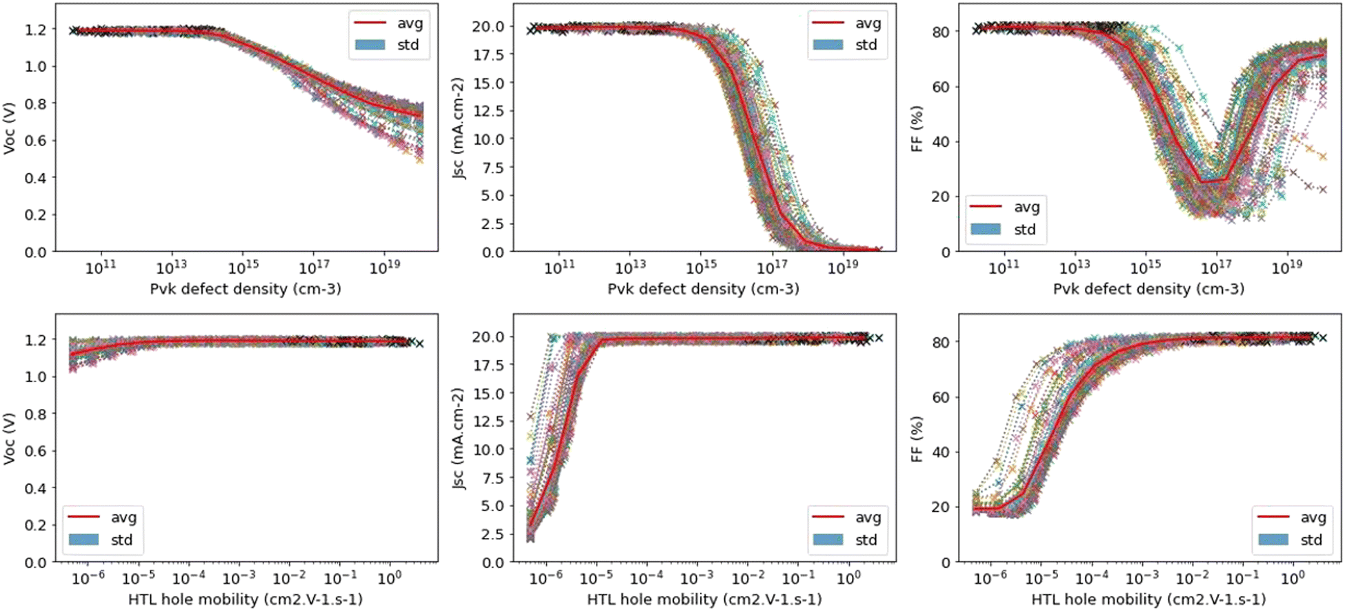 | ||
| Fig. 1 Evolution of Voc, Jsc and FF along two example degradation mechanisms: increase of defect density in the perovskite layer (top) and loss of hole mobility in the HTL (bottom). The response of each material parameter set is represented (98 in this example, all reproducing the initial performance of devices studied by Peng et al.). The clear similarity of evolutions allows us to compute an average behavior (red line) and 95% confidence interval (shaded area). | ||
Finally, average evolutions of electrical parameters are represented in Jscvs. Voc, FF vs. Voc and FF vs. Jsc graphs. Fig. 2 shows results associated to the devices studied by Peng et al., and Fig. S6 (ESI†) to other devices studied here. Importantly, the various scenarios induce different pathways: the three degradation mechanisms of the perovskite layer (increase of defect density in red, loss of electron or hole mobility in purple or brown) are distinguishable from each other in terms of Jsc/Voc and FF/Voc. Furthermore, coupling the three representations clearly allows distinguishing mechanisms: HTL/pvk interface degradation and ETL doping losses have close pathways in the Jsc/Voc graphs, but are almost orthogonal in FF/Voc graphs. Regions described by the confidence intervals indicate the potential reliability of the distinctions between degradation mechanisms. Noticeably, mechanisms associated to electron transport and hole transport are not symmetric, even when comparing nip and pin devices. This stems from the significantly distinct bandgaps and electron affinities of HTLs and ETLs, which are the parameters taken from the literature, causing the asymmetry between materials. Mechanisms are therefore not associated to the “front-contact” or the “back-contact”, but to the HTL or to the ETL.
 | ||
| Fig. 2 Degradation pathways of simulated degradation mechanisms in Jsc/Voc (left), FF/Jsc (center) and FF/Voc (right) planes. For each mechanism, the average behavior (over the 98 material parameters sets reproducing the devices studied by Peng et al.) is represented with squares and dashed lines, and shaded areas represent the 95% confidence interval. Pathways allow us to distinguish the mechanisms, while being independent from activation processes and environmental conditions. | ||
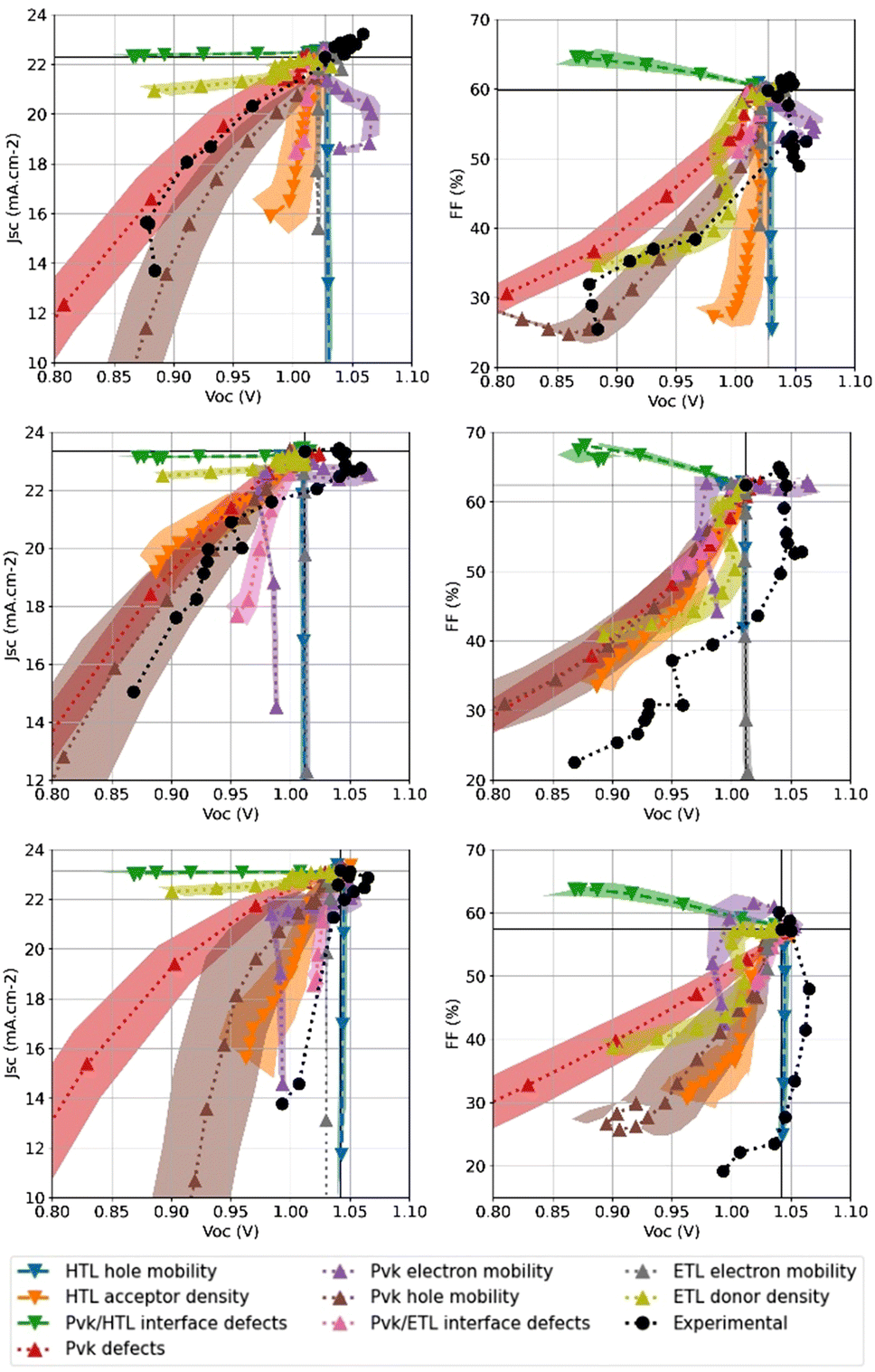
Degradation of Cs0.05FA0.88MA0.07PbI2.56Br0.44 based devices published by Peng et al.
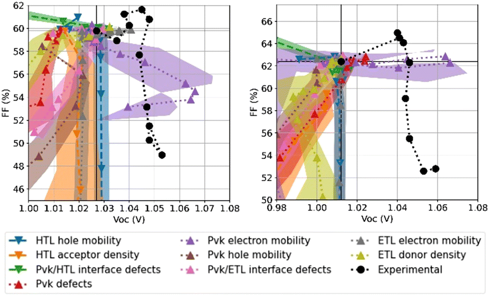
The method presented here has been used to analyze record devices: results published by Peng et al. established the highest reported efficiency for perovskite solar cells.31 They studied Cs0.05FA0.88MA0.07PbI2.56Br0.44-based perovskite solar cells (see details in Table S1, ESI†) and focused on both ETL and HTL to optimize the performance and stability. The results used here were recorded with encapsulated solar cells with a Spiro-OMeTAD HTL layer, aged during a damp-heat test: 85 °C, 85% relative humidity under dark. In fact, the authors studied devices with Spiro-OMeTAD and P3HT:CuPc HTL, the latter being significantly more stable. Instability of doped Spiro-OMeTAD has been widely reported, it is therefore coherent to correlate it with the degradation observed here. Accordingly, authors attributed the degradation of electrical performances to a deterioration of the HTL/perovskite interface, caused by lithium-ion diffusion (Spiro-OMeTAD dopant).The initial performances of the devices with Spiro-OMeTAD HTL were reproduced with 98 different material parameters sets and the associated JV curves are presented in Fig. S4 (ESI†). Simulated degradation pathways are displayed in Fig. S6 (ESI†). On the left in Fig. 3, the experimental Jsc/Voc pathway resembles a loss of hole mobility in the perovskite layer (brown). This mechanism is also a coherent explanation on the FF/Voc plane: although the FF drop is less pronounced at first, the final stage of degradation meets the simulated pathway. See Fig. S7 (ESI†) for the FF/Jsc plane. Another interpretation of these results arises by looking at only the three first points: they describe a significantly distinguishable trend (which is already observable when the results are displayed against time by the authors). This first part of degradation is close to the simulated pathway for a formation of defects at ETL/perovskite interface (pink), on all three planes.
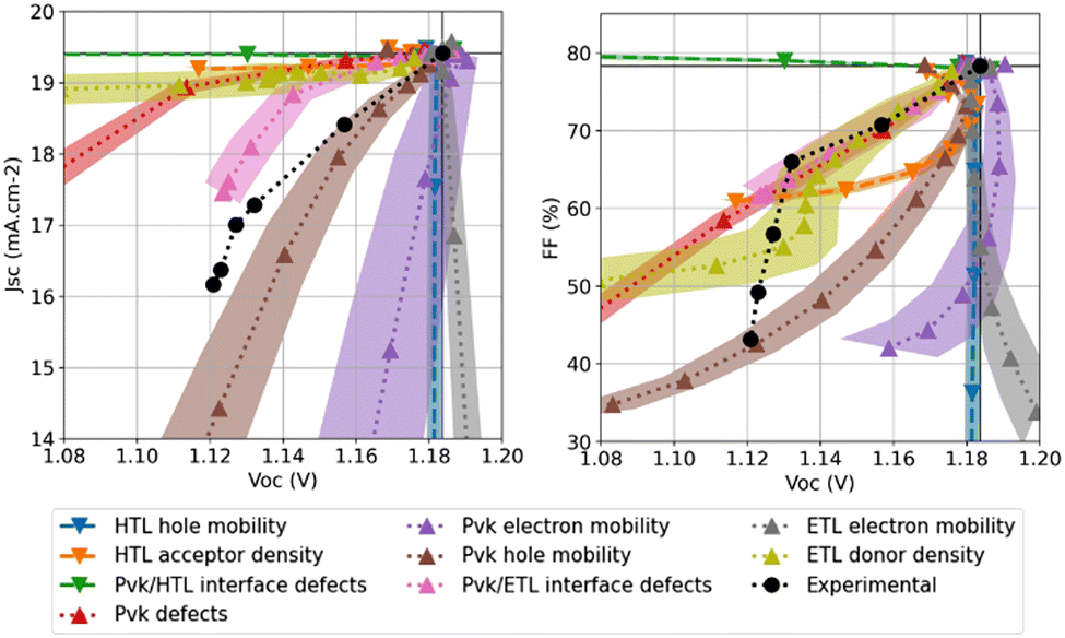 | ||
| Fig. 3 Experimental degradation pathways from results published by Peng et al.: perovskite devices were aged under dark conditions, at 85 °C and 85% relative humidity. Associated simulated pathways (average over 98 material parameter sets used to reproduce the initial performances) are superposed (downward facing triangles and dashed lines for causes identified by authors, upward facing triangles and dotted lines for others). A formation of defects at the ETL/perovskite interface (pink) or a decrease of hole mobility in the perovskite layer (brown) are the two closest mechanisms explaining experimental degradation. | ||
Devices with P3HT:CuPc HTL have also been investigated, and the details are reported in Table S4 (ESI†). A reproduction of the initial performance is displayed in Fig. S8 (ESI†) and degradation pathways in Fig. S9 (ESI†). Interestingly, the experimental pathway is close to a loss of hole mobility in the perovskite layer (brown), similarly to devices with a Spiro-OMeTAD HTL. This would be coherent with the fact that both structures rely on the same perovskite material, potentially being the “limiting factor” for the stability of electrical performances.
As a result, the analysis done here questions the causality of HTL degradation on electrical performance losses. Reduction of HTL hole mobility or doping (blue or orange) and perovskite/HTL interface deterioration (green) are very distinct from experiments. The loss of mobility does not induce Voc variation, and the loss of doping and interface deterioration does not induce Jsc losses. Therefore, these three mechanisms could difficultly explain the performance losses reported here. This interpretation doesn’t oppose a concomitant degradation of HTL: it can still have occurred without being the main cause of performance degradation.
Degradation of FA0.9Cs0.1PbI3 based devices published by Li et al.
The next results published in the literature analyzed here have been reported by Li et al., and they studied the degradation of unencapsulated, FA0.9Cs0.1PbI3 based devices (see details in Table S1, ESI†) under a N2 atmosphere during 600 h. Among other degradation conditions, the cells were kept under one sun illumination, at 35 °C, and were tracked at maximum power point (MPP) or kept at open circuit (Voc). For each aging condition, eight devices were used, and their JV characteristics recorded periodically. Finally, the authors reported their average result. Furthermore, they performed X-ray diffraction (XRD) measurements, performed PL- and synchrotron-based X-ray fluorescence microscopy with nanoscale spatial resolution to evidence phase segregation of the perovskite material (distinct Cs-rich and FA-rich areas). Furthermore, the combination with X-ray beam induced current measurements showed that Cs-rich areas are photo-inactive and current blocking. In addition, authors also focused on HTL and gold back contact. They re-coated aged samples with fresh HTL and gold and measured the PCE. For some samples, they degraded the full cell and removed aged HTL and gold. For other samples, they aged half stacks without HTL and gold from the beginning. As a result, Li et al. conclude that the main source of electrical performance degradation is the phase segregation of the perovskite itself, not being specifically triggered by HTL or gold.In the present study, the initial reported performances were reproduced with 104 and 125 different material parameter sets for the cells aged at MPP and Voc respectively, and the associated JV curves are presented in Fig. S4 (ESI†). First, degradation pathways have been derived for both cases separately. It appears that the pathways are similar for both groups of devices, which is coherent with the fact that they were fabricated in the same batch, with similar performances. Therefore, average responses over all simulations for both groups are computed, and associated pathways are used to analyze together both experimental results. Experimental pathways are superposed on Fig. 4 and the similarity of both experimental results indicates that similar dominant degradation mechanisms occurred. Furthermore, on the Jsc/Voc plane (top left), the closest mechanisms to experimental points are defect formation in the perovskite layer (red), or the loss of doping in the ETL (yellow) to the extent of the Voc loss being more consistent with the first one. This is confirmed by the FF/Voc and FF/Jsc graphs (see Fig. S6 (ESI†) for the FF/Jsc plane), showing better agreement of the experimental behavior with defect formation in the perovskite layer (red). On the FF/Voc graph, the loss of doping in the ETL (yellow) is significantly different because it starts with a sharp decrease of FF without Voc loss.
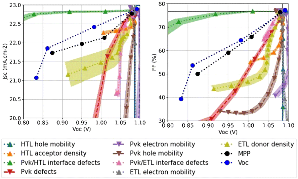 | ||
| Fig. 4 Experimental degradation pathways from the results published by Li et al.: devices were aged under one sun, N2 atmosphere, at 35 °C and tracked at maximum power point or kept at an open circuit voltage. Mean values over eight devices are reported for both conditions. Associated simulated pathways are superposed (downward facing triangles and dashed lines for causes identified by the authors, and upward facing triangles and dotted lines for others). The formation of defects in the perovskite layer (red) is the closest mechanism explaining the experimental degradation. | ||
The formation of defects in the perovskite layer is consistent with the phase segregation identified by Li et al. In fact, this spatially resolved phenomenon cannot be simulated with 1D drift diffusion simulations. However, the results obtained here show that even if all possible mechanisms cannot be simulated, the analysis presented here can help to identify the faulty layer or interface.
Degradation of Cs0.7FA0.3PbI2Br based devices published by Chen et al.
Chen et al. optimized the composition of Cs1−xFAxPbI2Br perovskites and studied the stability of associated devices. The results analyzed here were obtained with x = 0.3 (see the details in Table S1, ESI†) and devices were kept unencapsulated under an ambient atmosphere. As a result, other compositions were proved to be all less stable and more prone to phase change. The authors measured the photoluminescence spectra and decays on fresh and aged cells, as well as XRD spectra on fresh and aged perovskite films. They conclude that the composition with x = 0.3 delayed the phase change the most. The initial performances of these most stable devices were reproduced with 87 different material parameters sets, and the associated JV curves are presented in Fig. S4 (ESI†). The simulated degradation pathways are displayed in Fig. S6 (ESI†), and the measured degradation pathways are superposed in Fig. 5. Although a noisy experimental pathway, the closest simulated mechanism is the reduction of electron mobility in the perovskite layer (purple). See Fig. S7 (ESI†) for the FF/Jsc plane. On the other hand, the authors explained the improvement of efficiency during the experiment by better charge collection, coming from better interfaces and stress relaxation (supported by a higher photoluminescence intensity and longer carrier lifetime). This, however, would not explain the degradation observed during the whole experiment. Supplementary “degradation” mechanisms have been simulated for this example, considering respectively reductions of defect densities at the perovskite/HTL and perovskite/ETL interface. It appears in Fig. 5 (and Fig. S7, ESI†) that a rise in FF is associated with the healing of the perovskite/HTL interface, contrary to the lowering tendency in experimental results. Furthermore, the perovskite/ETL interface healing does not induce the rise of Voc observed experimentally.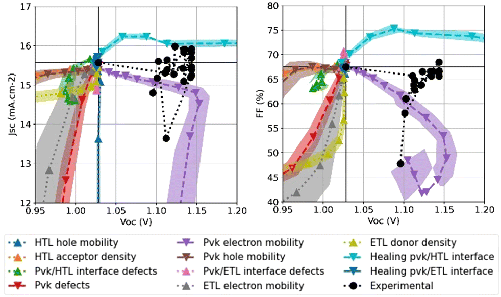 | ||
| Fig. 5 Experimental degradation pathways from the results published by Chen et al.: perovskite devices were unencapsulated and aged under ambient conditions. Associated simulated pathways (average over 87 material parameters sets used to reproduce initial performances) are superposed (downward facing triangles and dashed lines for the causes identified by the authors, and upward facing triangles and dotted lines for others). A decrease of electron mobility in the perovskite layer (purple) is the closest mechanism explaining experimental degradation. | ||
Therefore, the analysis here directly suggests the cause of the reduction of power conversion efficiency: even with the best composition the perovskite layer itself is the cause. This paves the way for further work on device stability by showing that focusing on the perovskite is still necessary, after the first optimization step reported by Chen et al.
Degradation of FA0.95MA0.05PbI2.85Br0.15 based devices published by Lim et al.
In order to understand the mechanisms occurring during degradation, Lim et al. focused on the kinetics of the degrading electrical parameters. In the fourth experimental study analyzed here; devices are semi-transparent encapsulated cells with a FA0.95MA0.05PbI2.85Br0.15 layer (see details in Table S1, ESI†). They are exposed to air under one sun at constant temperature, ranging from 25 to 70 °C. Importantly, all JV characteristic measurements were performed at 25 °C, even if the devices were aged at a higher temperature. Therefore, all simulations in this work were also done at 25 °C. The objective of the study was to study the thermal activation of the perovskite degradation. The authors determined the reaction rates at each temperature and deduced activation energies with an Arrhenius law. Importantly, it is necessary to presuppose that the same mechanism is occurring and being activated at all measurement temperatures. This will be discussed, as the method employed here allows us to distinguish mechanisms at each temperature. Furthermore, the authors combined XRD and cross-sectional scanning electron microscopy to compare the perovskite material properties before and after degradation. They noted the absence of formation of PbI2, as a sign for stability. Similarly, UV-visible spectroscopy measurements carried out before and after aging are analyzed. They support oxidation of the Spiro-OMeTAD HTL, together with iodide ion diffusion from the perovskite towards the HTL. As a result, the authors attributed the main cause of performance losses to the degradation of the HTL.The initial performances of the devices aged at 40, 55 and 70 °C were reproduced with respectively 101, 109 and 49 different material parameter sets. See the associated JV curves in Fig. S4 (ESI†) and the simulated degradation pathways in Fig. S6 (ESI†). In Fig. 6, experimental data recorded at 40 and 55 °C follow a behavior close to a loss of hole mobility (brown) or a formation of defects (red) in the perovskite layer, see Fig. S7 (ESI†) for all planes. Noticeably, the behavior tends to be different at 70 °C, with a lower variation of Voc and a more distinct fall of both other parameters. As a result, a loss of hole mobility in the HTL (blue) appears to be a closer mechanism.
 | ||
| Fig. 6 Experimental degradation pathways from the results published by Lim et al.: perovskite devices were aged under one sun, air and at 40, 55 or 70 °C (top, middle, and bottom respectively). Associated simulated pathways (average over 101, 109 and 49 material parameter sets used to reproduce the initial performances) are superposed (downward facing triangles and dashed lines for the causes identified by the authors, and upward facing triangles and dotted lines for others). Two distinct behaviours are visible. At 40 and 55 °C, the closest mechanisms are a loss of hole mobility (brown) or a formation of defects (red) in the perovskite layer. At 70 °C, a reduction of hole mobility in the HTL (blue) is closer to the experimental results. | ||
The fact that distinct degradation mechanisms occurred at different temperatures questions the kinetics approach used by the authors, which aims at studying the thermal activation of a given process. However, the higher temperature record has a significantly different pathway. If only thermal activation of the same mechanism had been involved, the same pathway would have simply been followed at a different speed.
Moreover, experimental data show a two-step trend: first a clear increase of open circuit voltage associated with low or positive variations of Jsc and FF, followed by a decrease of all parameters. This feature motivates us to study these results in two steps, extracting first the time period with a Voc increase, and then considering the second part as being a distinct device, starting from another point. This would correspond to a plausible situation in which a first mechanism has the main impact on electrical performances during the first part of the experiment, and a second one drives the evolution during the second step.
The first part of degradation is simply analyzed by considering the first experimental points, with the same simulated behaviors, as shown in Fig. 7. A loss of perovskite electron mobility (purple) can explain this behavior: an increase of Voc and a decrease of FF (see Fig. S10 (ESI†) for all planes at all temperatures). It is worth noting that at this step, degradations at all temperatures induce comparable paths, advocating the same mechanism, and being compatible with the kinetics approach.
 | ||
| Fig. 7 Experimental degradation pathways from the results published by Lim et al., distinguished into two successive parts and measured at 40 and 55 °C (left and right). Respective associated simulated pathways are superposed. Only the first part of the experimental degradation is extracted until respectively 475 and 175 minutes. The pathways are close to a loss of perovskite electron mobility (purple). | ||
In order to simulate degradation pathways for the second step, the procedure has been applied to the partially degraded devices, as if they were new fresh devices with lower performances, as presented in Table S5 (ESI†). This time, the performances of devices aged at 40, 55 and 70 °C were reproduced with respectively 72, 74 and 87 material parameter sets. The associated JV curves are presented in Fig. S11 (ESI†) and simulated degradation pathways in Fig. S12 (ESI†). Contrary to the first part of degradation, Fig. 8 shows two distinct trends at distinct temperature levels. At 40 and 55 °C, the increase of defect density (red) is confirmed by very good agreement of the experimental and simulated pathways on all three planes (see Fig. S12 (ESI†) for the FF/Jsc graph). However, at 70 °C, a reduction of acceptor density in the HTL (orange) would be a closer mechanism. In fact, two other mechanisms related to extracting layers are close to the experimental results, as they all induce almost no Voc loss: reduction of mobility in the HTL (blue) and in the ETL (grey). Interestingly, this analysis is coherent with the authors’ findings.
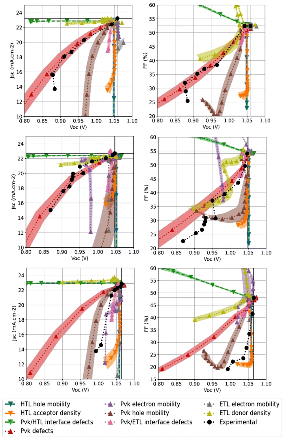 | ||
| Fig. 8 Experimental degradation pathways from the results published by Lim et al., distinguished into two successive parts and measured at 40, 55 and 70 °C (top, middle and bottom respectively). The associated simulated pathways are superposed. The second degradation step is analyzed as a new device with low initial performances. 72, 74 and 87 material parameter sets are used to derive new degradation pathways from the new starting points. The formation of defects in the perovskite layer (red) is the closest mechanism at lower temperatures and the experimental pathway at 70 °C is close to a reduction of acceptor density in the HTL (orange). | ||
This second step impacts device performances much more than the first one: approximatively 40 and 60% of Jsc and of FF losses, respectively, versus almost no Jsc variation and a 20% loss of FF during the first step. This explains why the interpretation with a single mechanism leads to comparable conclusions.
Finally, the analysis done here with the results published by Lim et al. shows well the strength of the proposed method. It is not necessary to use heavy characterization techniques to question the kinetics approach of the authors. Furthermore, the two step analysis shows that it is possible to consider several degradation mechanisms, impacting performance sequentially. The degradation mechanism proposed by Lim et al., involving the degradation of the HTL could be responsible for the performance losses, but only in combination with another mechanism, and only at higher temperatures. This shows that directly studying the causality of the degradation mechanisms instead of concomitance with material evolutions strengthens the analysis.
Conclusions
Studying the degradation of perovskite solar cells is becoming a key topic in the photovoltaic community. Now, optoelectrical parameters such as Jsc, Voc and FF are commonly recorded during degradation experiments of perovskite solar cells, but their dynamics are poorly used. Here, we present an innovative simulation method which helps identify the dominant mechanism. Correlations of electrical parameters are used to characterize the degradation and avoid time dependence and related potential activation effects. To do so, a procedure is established to obtain suitable sets of material parameters reproducing the initial performances of the studied device. This allows implementation of unitary degradation mechanisms on each of these sets. Finally, the average response to the mechanisms, over the material parameter sets, is derived, and directly compared to experimental data. First, the simulation results show that pathways associated with the investigated degradation mechanisms are clearly distinguishable. This shows that it is possible to characterize degradation of the perovskite solar cells through the evolution of the studied optoelectrical parameters. Second, the simulated paths are compared to the published experimental data, providing supplementary insights into the authors’ investigations.Record devices reported by Peng et al. are analyzed and guidelines for further stability improvements are obtained. Although HTL degradation is reported, we show that among the simulated mechanisms, performance losses are more likely attributable to mechanisms related to the perovskite material itself, showing that further improvement of the perovskite material stability itself is necessary. Here, the cause of electrical performance losses is directly investigated, instead of the concomitance with other phenomena, which is usually attained from degradation studies. Furthermore, the method presented here can confirm and/or question published analyses and provide new insights. Li et al. found that phase segregation degraded their devices and the work done here finds that the closest mechanism is the formation of defects. Chen et al. optimized the composition of the Cs-FA perovskite material, and it has been shown here that among the investigated cases, the perovskite material is still the most probable stability bottleneck of the device. Finally, Lim et al. studied the kinetics of optoelectronic parameters at several temperatures. This approach can be challenged, as results show distinct paths at different temperatures, indicating that potentially different mechanisms occurred. The versatility of the method also allows for the modelling of several mechanisms taking place sequentially, since one process may not be dominant throughout the degradation of the device. Analysis of the results from Lim et al. shows that it is possible that a single and same process occurred at all temperatures in a first step, but probably not in a second time.
Furthermore, this work paves the way for more advanced declinations by considering further optoelectrical parameters (for instance from photoluminescence, capacitance spectroscopy, or spectral response measurements). More elaborated degradation mechanisms, closer to the physical or chemical processes and consideration of spatial in-homogeneities and ionic migrations, can also be investigated. Finally, this work highlights the capabilities of advanced modeling for the analysis of perovskite degradation. Most significantly, identification of the mechanisms responsible for observed degradation is achieved by taking full advantage of time dependent measurements that are often only partly used. The causality of performance losses is successfully addressed and allows for the possibility of going beyond simply correlating the degradation with the state of device materials. After all, correlation is not causation, and it is through an improved understanding of the fundamental physics taking place that gains in terms of device stability are most likely to be achieved.
Author contributions
AJ developed the simulation procedure, performed the simulations, analyzed the data and wrote the article. JBP designed the study, discussed the numerical methods and results and proofread the article. JFG designed the study, designed and discussed the methods and results and proofread the article.Conflicts of interest
There are no conflicts to declare.Acknowledgements
This project was supported by the French Government in the Frame of the Program of Investment for the Future (Programme d’Investissement d’Avenir – ANR-IEED-002-01).Notes and references
- J. Huang, S. Tan, P. D. Lund and H. Zhou, Energy Environ. Sci., 2017, 10, 2284–2311 RSC.
- J. Hidalgo, C. A. Perini, A.-F. Castro-Mendez, D. Jones, H. Köbler, B. Lai, R. Li, S. Sun, A. Abate and J.-P. Correa-Baena, ACS Energy Lett., 2020, 5, 3526–3534 CrossRef.
- S. P. Dunfield, L. Bliss, F. Zhang, J. M. Luther, K. Zhu, M. F. A. M. Van Hest, M. O. Reese and J. J. Berry, Adv. Energy Mater., 2020, 1904054 CrossRef.
- C. C. Boyd, R. Cheacharoen, T. Leijtens and M. D. McGehee, Chem. Rev., 2019, 119, 3418–3451 CrossRef.
- J. Wei, Q. Wang, J. Huo, F. Gao, Z. Gan, Q. Zhao and H. Li, Adv. Energy Mater., 2021, 11, 35–37 Search PubMed.
- Z. Wang, Z. Zhang, L. Xie, S. Wang, C. Yang, C. Fang and F. Hao, Adv. Opt. Mater., 2022, 10, 2101822 CrossRef.
- L. Shi, M. P. Bucknall, T. L. Young, M. Zhang, L. Hu, J. Bing, D. S. Lee, J. Kim, T. Wu, N. Takamure, D. R. McKenzie, S. Huang, M. A. Green and A. W. Y. Ho-Baillie, Science, 2020, 368, 1–14 Search PubMed.
- N. Aristidou, C. Eames, I. Sanchez-Molina, X. Bu, J. Kosco, M. Saiful Islam and S. A. Haque, Nat. Commun., 2017, 8, 1–10 CrossRef.
- D. R. Ceratti, A. Zohar, R. Kozlov, H. Dong, G. Uraltsev, O. Girshevitz, I. Pinkas, L. Avram, G. Hodes and D. Cahen, Adv. Mater., 2020, 32, 2002467 CrossRef CAS.
- A. Bercegol, S. Cacovich, G. Vidon, S. Mejaouri, A. Yaiche, J. B. Puel, C. Longeaud, J. F. Guillemoles, S. Jutteau, J. Rousset, D. Ory and L. Lombez, J. Phys. Chem. C, 2020, 124, 11741–11748 CrossRef CAS.
- D. A. Jacobs, Y. Wu, H. Shen, C. Barugkin, F. J. Beck, T. P. White, K. Weber and K. R. Catchpole, Phys. Chem. Chem. Phys., 2017, 19, 3094–3103 RSC.
- Y. Yuan and J. Huang, Acc. Chem. Res., 2016, 49, 286–293 CrossRef CAS.
- J. A. Christians, P. Schulz, J. S. Tinkham, T. H. Schloemer, S. P. Harvey, B. J. Tremolet De Villers, A. Sellinger, J. J. Berry and J. M. Luther, Nat. Energy, 2018, 3, 68–74 CrossRef CAS.
- T. H. Schloemer, J. A. Christians, J. M. Luther and A. Sellinger, Chem. Sci., 2019, 10, 1904–1935 RSC.
- C. Xu, Z. Liu and E. C. Lee, J. Mater. Chem. C, 2021, 9, 679–686 RSC.
- M. Cheol Kim, S. Y. Ham, D. Cheng, T. A. Wynn, H. S. Jung and Y. S. Meng, Adv. Energy Mater., 2021, 11, 2001753 CrossRef.
- D. Messou, S. Cacocivh, S. Bechu, A. Yaiche, J. Rousset, P. Schulz and M. Bouttemy, 2020 47th IEEE Photovoltaic Specialists Conference (PVSC), 2021, 1628–1631.
- H. J. Lin, S. Cacovich, A. Rebai, J. Rousset and C. Longeaud, ACS Appl. Mater. Interfaces, 2020, 12, 19495–19503 CrossRef CAS PubMed.
- J. Peng, D. Walter, Y. Ren, M. Tebyetekerwa, Y. Wu, T. Duong, Q. Lin, J. Li, T. Lu, M. A. Mahmud, O. L. C. Lem, S. Zhao, W. Liu, Y. Liu, H. Shen, L. Li, F. Kremer, H. T. Nguyen, D. Y. Choi, K. J. Weber, K. R. Catchpole and T. P. White, Science, 2021, 371, 390–395 CrossRef CAS.
- N. Li, Y. Luo, Z. Chen, X. Niu, X. Zhang, J. Lu, R. Kumar, J. Jiang, H. Liu, X. Guo, B. Lai, G. Brocks, Q. Chen, S. Tao, P. David and H. Zhou, Joule, 2020, 4, 1743–1758 CrossRef CAS.
- M. Chen, S. R. Sahamir, G. Kapil, A. K. Baranwal, M. A. Kamarudin, Y. Zhang, K. Nishimura, C. Ding, D. Liu, D. Hirotani, Q. Shen and S. Hayase, Sol. Energy Mater. Sol. Cells, 2020, 218, 110741 CrossRef CAS.
- J. Lim, M. Kim, H. H. Park, H. Jung, S. Lim, X. Hao, E. Choi, S. Park, M. Lee, Z. Liu, M. A. Green, J. Seo, J. Park and J. S. Yun, Sol. Energy Mater. Sol. Cells, 2021, 219, 110776 CrossRef CAS.
- B. X. Zhao, C. Yao, K. Gu, T. Liu, Y. Xia and Y. L. Loo, Energy Environ. Sci., 2020, 13, 4334–4343 RSC.
- S. C. Ezike, A. B. Alabi, A. N. Ossai and A. O. Aina, Opt. Mater., 2021, 112, 110753 CrossRef.
- A. A. Zaky, E. Christopoulos, K. Gkini, M. K. Arfanis, L. Sygellou, A. Kaltzoglou, A. Stergiou, N. Tagmatarchis, N. Balis and P. Falaras, Appl. Catal., B, 2021, 284, 119714 CrossRef.
- M. V. Khenkin, E. A. Katz, A. Abate, G. Bardizza, J. J. Berry, C. Brabec, F. Brunetti, V. Bulović, Q. Burlingame, A. Di Carlo, R. Cheacharoen, Y. B. Cheng, A. Colsmann, S. Cros, K. Domanski, M. Dusza, C. J. Fell, S. R. Forrest, Y. Galagan, D. Di Girolamo, M. Grätzel, A. Hagfeldt, E. von Hauff, H. Hoppe, J. Kettle, H. Köbler, M. S. Leite, S. (Frank) Liu, Y. L. Loo, J. M. Luther, C. Q. Ma, M. Madsen, M. Manceau, M. Matheron, M. McGehee, R. Meitzner, M. K. Nazeeruddin, A. F. Nogueira, Ç. Odabaşı, A. Osherov, N. G. Park, M. O. Reese, F. De Rossi, M. Saliba, U. S. Schubert, H. J. Snaith, S. D. Stranks, W. Tress, P. A. Troshin, V. Turkovic, S. Veenstra, I. Visoly-Fisher, A. Walsh, T. Watson, H. Xie, R. Yıldırım, S. M. Zakeeruddin, K. Zhu and M. Lira-Cantu, Nat. Energy, 2020, 5, 35–49 CrossRef.
- J. Kim, N. Park, J. S. Yun, S. Huang, M. A. Green and A. W. Y. Ho-Baillie, Sol. Energy Mater. Sol. Cells, 2017, 162, 41–46 CrossRef.
- J. P. Bastos, G. Uytterhoeven, W. Qiu, U. W. Paetzold, D. Cheyns, S. Surana, J. Rivas, M. Jaysankar, W. Song, T. Aernouts, J. Poortmans and R. Gehlhaar, ACS Appl. Mater. Interfaces, 2019, 11, 16517–16526 CrossRef.
- J. Qian, M. Ernst, N. Wu and A. Blakers, Sustain. Energy Fuels, 2019, 3, 1439–1447 RSC.
- H. Sohrabpoor, G. Puccetti and N. E. Gorji, RSC Adv., 2016, 6, 49328–49334 RSC.
- M. A. Green, E. D. Dunlop, J. Hohl-Ebinger, M. Yoshita, N. Kopidakis and X. Hao, Prog. Photovoltaics Res. Appl., 2021, 30, 3–12 CrossRef.
- X. Xia, W. Wu, H. Li, B. Zheng, Y. Xue, J. Xu, D. Zhang, C. Gao and X. Liu, RSC Adv., 2016, 6, 14792–14798 RSC.
- M. Deepa, M. Salado, L. Calio, S. Kazim, S. M. Shivaprasad and S. Ahmad, Phys. Chem. Chem. Phys., 2017, 19, 4069–4077 RSC.
- D. K. Maram, M. Haghighi, O. Shekoofa, H. Habibiyan and H. Ghafoorifard, Sol. Energy, 2021, 213, 1–12 CrossRef.
- E. Raza, Z. Ahmad, F. Aziz, M. Asif, A. Ahmed, K. Riaz, J. Bhadra and N. J. Al-Thani, Sol. Energy, 2021, 225, 842–850 CrossRef CAS.
- J. Haddad, B. Krogmeier, B. Klingebiel, L. Krückemeier, S. Melhem, Z. Liu, J. Hüpkes, S. Mathur and T. Kirchartz, Adv. Mater. Interfaces, 2020, 7, 2000366 CrossRef.
- Y. H. Khattak, F. Baig, A. Shuja, S. Beg and B. M. Soucase, Sol. Energy, 2020, 207, 579–591 CrossRef.
- S. Karthick, J. Bouclé and S. Velumani, Sol. Energy, 2021, 218, 157–168 CrossRef.
- R. E. Brandt, R. C. Kurchin, V. Steinmann, D. Kitchaev, C. Roat, S. Levcenco, G. Ceder, T. Unold and T. Buonassisi, Joule, 2017, 1, 843–856 CrossRef.
- PV-Lighthouse, SunSolve, https://www.pvlighthouse.com.au/sunsolve, (accessed 15 December 2021).
- M. Burgelman, P. Nollet and S. Degrave, Thin Solid Films, 2000, 361–362, 527–532 CrossRef.
Footnote |
| † Electronic supplementary information (ESI) available. See DOI: https://doi.org/10.1039/d2ee03377a |
| This journal is © The Royal Society of Chemistry 2023 |