
Atomically flat semiconductor nanoplatelets for light-emitting applications
Bing
Bai†
a,
Chengxi
Zhang†
 b,
Yongjiang
Dou
b,
Lingmei
Kong
b,
Lin
Wang
b,
Sheng
Wang
b,
Jun
Li
a,
Yi
Zhou
a,
Long
Liu
a,
Baiquan
Liu
c,
Xiaoyu
Zhang
d,
Ido
Hadar
e,
Yehonadav
Bekenstein
f,
Aixiang
Wang
g,
Zongyou
Yin
h,
Lyudmila
Turyanska
i,
Jochen
Feldmann
j,
Xuyong
Yang
*b and
Guohua
Jia
*k
b,
Yongjiang
Dou
b,
Lingmei
Kong
b,
Lin
Wang
b,
Sheng
Wang
b,
Jun
Li
a,
Yi
Zhou
a,
Long
Liu
a,
Baiquan
Liu
c,
Xiaoyu
Zhang
d,
Ido
Hadar
e,
Yehonadav
Bekenstein
f,
Aixiang
Wang
g,
Zongyou
Yin
h,
Lyudmila
Turyanska
i,
Jochen
Feldmann
j,
Xuyong
Yang
*b and
Guohua
Jia
*k
aKey Lab for Special Functional Materials, Ministry of Education, National and Local Joint Engineering Research Center for High-Efficiency Display and Lighting Technology, School of Materials Science and Engineering, and Collaborative Innovation Center of Nano Functional Materials and Applications, Henaon University, Kaifeng 475004, China
bKey Laboratory of Advanced Display and System Applications of Ministry of Education, Shanghai University, Shanghai 200072, China. E-mail: yangxy@shu.edu.cn
cSchool of Electronics and Information Technology, Sun Yat-sen University, Guangzhou 510275, China
dKey Laboratory of Automobile Materials, Ministry of Education, College of Materials Science and Engineering, Jilin Provincial International Cooperation Key Laboratory of High-Efficiency Clean Energy Materials, Electron Microscopy Center, Jilin University, Changchun 130012, China
eInstitute of Chemistry, and the Center for Nanoscience and Nanotechnology, The Hebrew University of Jerusalem, Jerusalem 91904, Israel
fDepartment of Materials Science and Engineering, Technion-Israel Institute of Technology, Haifa 32000, Israel
gSchool of Chemistry and Chemical Engineering, Linyi University, Linyi 276005, P. R. China
hResearch School of Chemistry, The Australian National University, ACT 2601, Australia
iFaculty of Engineering, The University of Nottingham, Additive Manufacturing Building, Jubilee Campus, University Park, Nottingham NG7 2RD, UK
jChair for Photonics and Optoelectronics, Nano-Institute Munich and Department of Physics, Ludwig-Maximilians-Universität (LMU), Königinstr. 10, Munich 80539, Germany
kSchool of Molecular and Life Sciences, Curtin University, Perth, WA 6102, Australia. E-mail: guohua.jia@curtin.edu.au
First published on 19th December 2022
Abstract
The last decade has witnessed extensive breakthroughs and significant progress in atomically flat two-dimensional (2D) semiconductor nanoplatelets (NPLs) in terms of synthesis, growth mechanisms, optical and electronic properties and practical applications. Such NPLs have electronic structures similar to those of quantum wells in which excitons are predominantly confined along the vertical direction, while electrons are free to move in the lateral directions, resulting in unique optical properties, such as extremely narrow emission line width, short photoluminescence (PL) lifetime, high gain coefficient, and giant oscillator strength transition (GOST). These unique optical properties make NPLs favorable for high color purity light-emitting applications, in particular in light-emitting diodes (LEDs), backlights for liquid crystal displays (LCDs) and lasers. This review article first introduces the intrinsic characteristics of 2D semiconductor NPLs with atomic flatness. Subsequently, the approaches and mechanisms for the controlled synthesis of atomically flat NPLs are summarized followed by an insight on recent progress in the mediation of core/shell, core/crown and core/crown@shell structures by selective epitaxial growth of passivation layers on different planes of NPLs. Moreover, an overview of the unique optical properties and the associated light-emitting applications is elaborated. Despite great progress in this research field, there are some issues relating to heavy metal elements such as Cd2+ in NPLs, and the ambiguous gain mechanisms of NPLs and others are the main obstacles that prevent NPLs from widespread applications. Therefore, a perspective is included at the end of this review article, in which the current challenges in this stimulating research field are discussed and possible solutions to tackle these challenges are proposed.
 Bing Bai | Bing Bai is a lecturer in the School of Materials at Henan University, China. He received his PhD degree in 2021 from the School of Materials and Engineering, Beijing Institute of Technology. His research interests are the controlled synthesis of doped nanocrystals, especially the novel optical properties and applications caused by the hetero-valence impurities doped in II-VI nanocrystals. |
 Chengxi Zhang | Chengxi Zhang is a postdoc in the Key Laboratory of Advanced Display and System Applications of Ministry of Education at Shanghai University, China. He obtained his PhD degree in power engineering and engineering thermophysics in 2019 from East China University of Science and Technology, followed by the postdoctoral research at Shanghai University. His research focuses on the design and preparation of fluorescent nanomaterials, with a particular emphasis on the configuration of fluorescent nanomaterial ink, as well as their application in the various optoelectronic devices. |
 Ido Hadar | Ido Hadar is a senior lecturer (assistant professor) at the Hebrew University of Jerusalem, Israel. He received his PhD from the Hebrew University of Jerusalem (2016), followed by a post-doctoral fellowship at Northwestern University under the guidance of Prof. Mercouri Kanatzidis (2016–2020). His research focuses on novel semiconductor materials for applications such as light-emitting devices and high energy detectors. Specifically, he is interested in the correlation between the structure and dimensionality of such materials and their optoelectronic properties. |
 Yehonadav Bekenstein | Yehonadav Bekenstein is an assistant professor at Technion-Israel Institute of Technology, Israel. He received his PhD from the Hebrew University of Jerusalem (2015), followed by a post-doctoral fellowship at University of California, Berkeley under the guidance of Prof. Paul A. Alivisatos (2015–2018). His research focuses on metal halide perovskite materials, light–matter interactions at the nanoscale and nanocrystals. |
 Jochen Feldmann | Jochen Feldmann is leading the Chair for Photonics and Optoelectronics at Ludwig-Maximilians-Universität (LMU) in Munich and is the Director at the Nano-Institute Munich. He is a co-founder of the Center for NanoScience (CeNS), the Bavarian Energy Initiative Solar Technologies Go Hybrid, the German Excellence Clusters Nanosystems Initiative Munich (NIM) and e-conversion. His research focuses on nano-plasmonics, semiconductor optics and photonic applications of semiconductor nanocrystals. |
 Xuyong Yang | Xuyong Yang is a Full Professor (Eastern Scholar) in the Key Laboratory of Advanced Display and System Applications of Ministry of Education in Shanghai University, China. He received his PhD degree in microelectronics from Nanyang Technological University in Singapore in 2014 and worked as a postdoc at the same university prior to commencing his independent research career at Shanghai University. His research focuses primarily on the design and fabrication of low dimensional luminescent nanomaterials such as quantum dots and nanorods, as well as their application in various optoelectronic devices. |
 Guohua Jia | Guohua Jia is an associate professor at Curtin University, Australia. He obtained his PhD degree in chemistry in 2009 from City University of Hong Kong. Then he had been working as a postdoctoral fellow with Prof. Uri Banin at the Hebrew University of Jerusalem, Israel from 2010 to 2014. He commenced his current role as a group leader at Curtin University in 2015. His research interests focus on chemistry and physics of colloidal nanocrystals, with a particular emphasis on their shape-dependent properties and application in catalysis and optoelectronic devices. |
1. Introduction
When the size of semiconductor materials shrinks from the bulk to nanometer scale on any of their dimensions that is similar to or smaller than the normal size of the excited electron and hole pair (exciton) in the same bulk material (the Bohr radius), many unique optical properties emerge due to the quantum confinement effect.1–10 Depending on which dimension the excitons are confined in, semiconductor nanocrystals (NCs) fall into three categories, including zero-dimensional (0D) spherical quantum dots (QDs) with excitons being confined in all three dimensions, one-dimensional (1D) nanorods (NRs)/nanowires (NWs) with excitons being confined in two dimensions and two-dimensional (2D) nanoplatelets (NPLs)/nanosheets with excitons being confined in one dimension, resulting in a similar electronic structure to that of semiconductor quantum wells.11–14 Among all semiconductor NCs, isotropic II–VI QDs, such as CdS, CdSe, CdTe, ZnS, ZnSe and ZnTe, have been extensively studied in the last several decades.6,7,15–17 Compared to spherical QDs, 2D semiconductor NCs, known as NPLs, in which excitons are confined only along the vertical direction, possess unique optical properties, such as extremely narrow emission line width, short photoluminescence (PL) lifetime, high gain coefficient, giant oscillator strength transition (GOST) and so on.8,9,18 These fascinating properties in combination with the precise morphology and structure control of NPLs at the atomic level provide a solid basis for their potential in high color purity light-emitting applications.18–22 Being different from semiconductor quantum wells synthesized by chemical vapor deposition and molecular beam epitaxy, which require high vacuum and expensive instruments, semiconductor NPLs can be feasibly prepared using colloidal wet chemical methods, which means that they can be made using comparatively inexpensive processes and their syntheses are scalable.To date, a variety of semiconductor NPLs including CdS,23–25 CdSe,2,26–30 CdTe,31–33 ZnS,34,35 ZnSe36,37 and ZnTe38,39 with atomic flatness have been reported. The majority of the NPLs reported so far are II–VI semiconductor materials, and to date, no III–V semiconductor NPLs have been reported. This is likely because the synthesis of III–V NPLs usually requires harsh conditions including high reaction temperature, long reaction time and reacting precursors (both cation and anion) with suitable reactivities due to the highly covalent nature of III–V bonds. Among these II–VI NPLs, thickness control has been successfully accomplished for zinc blende CdS, CdSe and CdTe NPLs that allowed the tuning of the emission wavelengths of such NPLs in the visible spectral range,25,26,31,40–42 thus endowing them with the potential for light-emitting applications. To avoid confusion, we herein treated a layer of semiconductor NPLs containing two atomic layers (cations and anions) as a monolayer (ML). Despite significant progress in the controlled synthesis of zinc blende Cd-based NPLs, it seems that zinc blende Zn chalcogenide NPLs are still inaccessible because of the narrow growth window parameters of such materials. On the other hand, although wurtzite II-VI NPLs with a unique thickness of 4 MLs have been obtained, to date, the preparation of wurtzite II-VI NPLs with thickness larger than 4 MLs was not possible.38 Pang et al.38 employed density functional theory to calculate the formation energy for the growth of wurtzite NLs thicker than 4 MLs by assuming that the growth of wurtzite NPLs was conducted in methylamine to simplify the calculations although the reactions were carried out in oleylamine. The obtained energy barrier in the thickness growth process of NPLs from 4 MLs to 4.5 MLs is very high, which may be affected by the large difference in the binding capability of the surfactants between methylamine and oleylamine. Further discussion relating to the thickness control of wurtzite NPLs will be elaborated in more detail in the following sections of this article.
Semiconductor NCs have lots of surface dangling bonds that may form surface trap states for charge carriers and thereby reduce the PL quantum yield (PLQY). An effective method to tackle this issue is to overgrow passivation layers of another semiconductor on the surfaces of semiconductor NCs, producing a prototype system with a core/shell configuration, wherein the shells significantly improve the PLQY and stability against photobleaching.43–45 For anisotropic NPLs, depending on which plane the passivation layers grow, the combination of NPL cores and the passivation layers results in heterostructures with three types of configurations, such as a core/shell structure with all planes being passivated,46 a core/crown structure with sidewalls being passivated47 and a core/crown@shell structure with all planes of core/crown structure being passivated.48 Compared to spherical QDs, semiconductor NPLs exhibit an ultra-narrow emission line width (full width at half maximum (FWHM) = 4–17 nm) originating from the atomic flatness of the NPL basal planes.23,37,49,50 The red-emitting CdSe/CdZnS core/shell NPLs enabled the extremely saturated red color LEDs with the Commission Internationale de L’Eclairage (CIE) coordinates of (0.715, 0.283).18 Additionally, semiconductor NPLs possess GOST because of the one-dimensional confinement of charge carriers9,18,50,51 and GOST can enhance the gain coefficient of NPLs.52 A giant net modal gain coefficient as high as ∼6600 cm−1 was obtained in CdSe NPLs,53 which made NPLs as ideal materials for amplified spontaneous emission (ASE) and lasers with a low threshold.54 The short PL lifetimes of NPLs, which are about several nano seconds, provide another advantage of NPLs for lasers.8 Besides the ultra-narrow emission line width, high gain coefficient and short PL lifetime, semiconductor NPLs also exhibit fast fluorescence resonance energy transfer (FRET) processes of several picoseconds to tens of picoseconds,55–57 which are much faster than the Auger recombination (AR) processes (several hundreds of picoseconds),58 and thus have the potential in reduced threshold optical gain media and multi-exciton solar cells.
This review provides a comprehensive overview on the synthesis of semiconductor NPLs with atomic flatness, unique optical properties and stimulating applications in light-emitting devices. In the first section of this review article, the intrinsic characteristics of NPLs, such as atomically controlled thicknesses, 1D confinement and the GOST effect, will be elaborated. Subsequently, we will focus on the synthesis of NPLs, including synthetic methods, growth mechanisms and the morphology control. In the third section, we will provide an overview on the structure and surface engineering of NPLs, including crystalline phase, doping, alloying, core/shell, core/crown, core/crown@shell and surface ligands. We then present the NPL-based light-emitting devices, such as LEDs, backlight for LCDs and lasers, based on the unique optical properties enabled by the atomically flat basal planes of NPLs. Finally, we will provide our visions on the challenges and outlooks in this stimulating and burgeoning research field.
2. Intrinsic characteristics
2.1 Atomically controlled thickness
For typical semiconductor NPLs, the size on the vertical direction is much smaller than their lateral size and thereby excitons are predominantly confined in the thickness direction while the confinement of excitons on the lateral directions is negligible.9,14,50,52 The confinement direction and the lateral dimension of semiconductor NPLs can be inferred from the XRD diffraction patterns of the corresponding lattice planes of such NPLs because the widths of the XRD peaks become broadened unevenly due to highly anisotropic 2D morphology of the crystallites.59,60 For example, since the (002) plane of zinc blende CdSe NPLs has a very large breadth, its intensity is very weak and the diffraction feature of this lattice plane almost diminishes and hard to be recognized from the background of the diffraction patterns. As for the diffraction peak of (002) of wurtzite CdSe NPLs, its width becomes much sharper compared with those of other lattice planes because such NPLs have the largest dimension along the [002] direction.27 Notably, the key feature of NPLs that is different from that of their counterparts such as 0D QDs and 1D NRs/NWs is their atomic flatness. Although there are very few studies that have investigated the origins of the formation of such surfaces, the underlying mechanisms that underpin the growth of atomic flat surfaces in NPLs could be likely proposed. For example, growth along the lateral directions of CdSe NPLs with a given thickness is energy spontaneous while that along their vertical (thickness) direction is energy unfavorable,61 which may result in atomic flatness. Such feature of semiconductor NPLs manifests in both extremely sharp excitonic absorption peaks and ultra-narrow emission line width.23,26–28,62,63 So far, atomically thick semiconductor NPLs with diverse chemical compositions, including CdS,24,25,64 CdSe,26–28 CdTe,31,33 ZnS,35 ZnSe,36,38 ZnTe39 and PbS,65–67 have been synthesized using wet chemical synthetic approaches. In the case of core-only CdSe NPLs, the FWHMs of PL emission peaks are not broader than 17 nm (Table 1), which is significantly narrower than those of their counterparts such as spherical CdSe QDs.61,68,69 The thickness of zinc blende CdSe NPLs can be precisely tuned in a range from 2 to 8.5 MLs, enabling the tunable emissions across the visible region.41,42,70 However, since NPLs adopt a layer-by-layer growth mode, their thicknesses are quantized instead of successive, resulting in quantized peak positions.| NPLs | PL peak positions | PLQYs | FWHMs of emission peaks | Lifetimes | Stokes shifts | Reaction conditions for NPLs |
|---|---|---|---|---|---|---|
| CdSe26 | 462 ± 2 nm | 30% | 10 nm | — | <10 meV | Cd(myr)2, Se powder, Cd(OAc)2, 195–240 °C, 10 minutes. |
| 512 ± 2 nm | ||||||
| 550 ± 2 nm | ||||||
| CdSe28 | 460 nm | 50% | 7 nm | — | <2 nm | Cd(OAc)2, oleic acid (OA), Se powder, tri-n-octylphosphine (TOP), 170 °C, 45 minutes. |
| CdSe23 | 550 nm | 40% | <35 meV | 3.99 ns | 0 nm | Cd(myr)2, Se powder, Cd(OAc)2, 240 °C, 10 minutes. |
| CdSe41 | 509.9 nm | 26% | 9.3 nm | 5.3 ns | 2.2 nm | Cd(myr)2, CdCl2, CdOlAc, Se powder, 220–320 °C, 10 minutes-5 hours. |
| 554.0 nm | 18% | 8.8 nm | 8.6 ns | 1.9 nm | ||
| 583.7 nm | 14% | 9.7 nm | 8.4 ns | 2.4 nm | ||
| 606.6 nm | 16% | 11.3 nm | 10.9 ns | 2.8 nm | ||
| 625.3 nm | 11% | 13.1 nm | 10.8 ns | 2.4 nm | ||
| CdSe40 | 585 nm | 45% | 9 nm | 4.3 ns | 7 meV | Cd(myr)2, Cd(OAc)2, CdCl2, Se powder, 250 °C, 5 minutes. |
| CdSe74 | 582 nm | 50% | 11 nm | 5.3 ns | 2 nm | CdO, Cd(OAc)2, CdF2, Se powder, myristic acid, 280 °C, 40 minutes. |
| CdTe31 | 428–556 nm | <1% | ≤7 nm | — | 0 nm | Cd(prop)2, TOP-Te, OA, 180–215 °C, 15–30 minutes. |
| ZnSe37 | 345 nm | — | 4 nm | — | — | ZnSt2, Se powder, oleylamine (OAm), octylamine,170 °C, 6–8 hours. |
| 380 nm | 4.4 nm | |||||
| PbS65 | 735–748 nm | — | 48–68 nm | 8.4–59 ns | 18–20 nm | Pb(NO3)2, octadecanol, trioctylamine, CS2, 80 °C, 20 hours. |
| CdSe/CdS75 | 667 nm | 50–60% | 20 nm | — | — | Core: Cd(myr)2, Cd(OAc)2, Se powder, 240 °C, 8 minutes. |
| Shell: Cd(oleate)e, OAm, 1-octanethiol, 300 °C, 2 hours. | ||||||
| CdSe/CdZnS core/shell76 | 632 nm | 60% | 20 nm | — | 8 nm | Core: Cd(OAc)2(H2O)2, Se powder, OA, 240 °C, 15 minutes; shell: thioacetamide, octylamine, Cd(NO3)2, Zn(NO3)2, room temperature, 24 hours. |
| CdSe/CdZnS core/shell71 | 510–630 nm | 30–80% | 37–65 meV | 4–15 ns | — | Core: Cd(OAc)2(H2O)2, Se powder, OA, 240 °C, 15 minutes; shell: Cd(OAc)2(H2O)2, Zn(NO3)2·H2O, Na2S, room temperature. |
| CdSe/Cd0.25Zn0.75S core/shell77 | ∼650 nm | ∼100% | 20–24 nm | — | — | Core: Cd(myr)2, Cd(OAc)2, Se powder, 240 °C, 9 minutes; shell: Cd(OAc)2, Zn(OAc)2, OA, OAm, 1-octanethiol, 300 °C, 50 minutes. |
| CdSe/CdxZn1−xS core/shell78 | 692 nm | 92% | 22.1 nm | 22 ns | — | Core: Cd(myr)2, Cd(OAc)2, Se powder, 204–250 °C, 6–9 minutes; shell: Cd(oleate)e, Zn(oleate)2, OAm, 1-octanethiol, 300 °C,40 minutes. |
| CdSe1−xSx/CdxZn1−xS core/shell79 | 554–615 nm | 33–90% | 25–30 nm | 16.98–39.53 ns | — | Core: Cd(myr)2, Cd(OAc)2, Se powder, octadecene (ODE)-S, 204 °C, 10 minutes; shell: Cd(OAc)2, Zn(OAc)2, OA, OAm, 1-octanethiol, 300 °C, 1 hour. |
| CdSe/ZnS core/shell80 | 616 nm | 98% | 27 nm | 6 ns | — | Core: Cd(myr)2, Cd(OAc)2, Se powder, 240 °C, 10 minutes; shell: Zn(OAc)2, OA, OAm, 1-octanethiol, 300 °C, 1 hour. |
| CdSe/CdS core/crown73 | 510–540 nm | 60% | 13–14 nm | — | — | Core: Cd(myr)2, Cd(OAc)2, TOP-Se, Se powder, OA, 170–250 °C, 10 minutes; crown: Cd(OAc)2·H2O, ODE-S, OA, 230–250 °C. |
| CdSe/CdS@Cd1−xZnxS core/crown@shell81 | ∼614 nm | 45–60% (NMF) | 66 meV | 13 ns (NMF) | — | Core: Cd(myr)2, Se powder, 240 °C, 10 minutes; crown: Cd(OAc)2·H2O, ODE-S, OA, 240 °C; shell: Cd(NO3)2, Zn(NO3)2, (NH4)2S, room temperature. |
| 55–75% (toluene) | 68–70 meV | 11 ns (toluene) | ||||
| 70–90% (water) | 35 ns (water) | |||||
| CdSe/CdS@CdS core/crown@shell48 | 480 nm | 90% | 62–90 meV | 2.72–3.28 ns | — | Core: Cd(myr)2, Se powder, 240 °C, 10 minutes; crown: Cd(OAc)2, OA, ODE-S, 240 °C; shell: Cd(OAc)2, (NH4)2S, room temperature. |
| 511 nm | ||||||
| CdSe/CdS/CdTe core/barrier/crown82 | 510 nm | — | 11.2–13.6 nm (CdSe band edge) | 3.9 ns | Core: Cd(myr)2, Se powder, 240 °C, 8 minutes; barriers: Cd(OAc)2·H2O, Cd(propionate)2, ODE-S, OA, 235 °C; crown: Cd(propionate)2, TOP-Te, OA, 235 °C. | |
| 575 nm | 74.8–109.6 nm (indirect exciton transition) | 76 ns | ||||
| 625 nm | 182 ns | — |
Interestingly, the construction of core/shell and core/crown structures does not alter the atomic flat nature of NPLs. Although slight broadening of emission line width is observed in core/shell NPLs, the atomic flatness is retained.23,71 The intrinsic large exciton–phonon coupling and the electron shakeup result in the slight broadening of the emission line width,71,72 which will be discussed later in this review. In a typical CdSe/CdS core/crown structure, a CdS crown is laterally extended on the sidewalls of a CdSe NPL core. Therefore, both core and crown possess the same thickness and the atomic flatness of core/crown structure is preserved, as indicated by the ultra-narrow emission line width.73
2.2 Thickness-dependent band gap relating to one-dimensional confinement
Fig. 1 shows the schematic illustration of bulk, 2D, 1D and 0D materials. The electronic density of states (DOS) is utilized to quantify the distribution of energy levels that can be occupied by the electrons in a quasiparticle picture. For semiconductor materials, the density of free charge carriers can be calculated by the electronic DOS, which serves as an indirect proxy for the properties such as energy band gap, band energy and optical absorption spectrum.83 In the solid-state DOS, D(E) of any material is the number (N) of available electronic states per unit volume per unit energy around an energy E and can be expressed as . The DOS structure depends on the dimensions (Fig. 1). For 2D semiconductor materials, the free electrons are confined along the z axis, splitting the band into subbands and leaving two continuously varying wave vectors.12 The DOS of 2D materials transforms to a step-like energy spectrum from the smooth energy spectrum of bulk materials.12 The energy difference (ΔE) of two adjacent energy levels is mainly determined by the magnitude of the quantum size effect. ΔE can be calculated for each confined dimension using the following equation:
 | (1) |
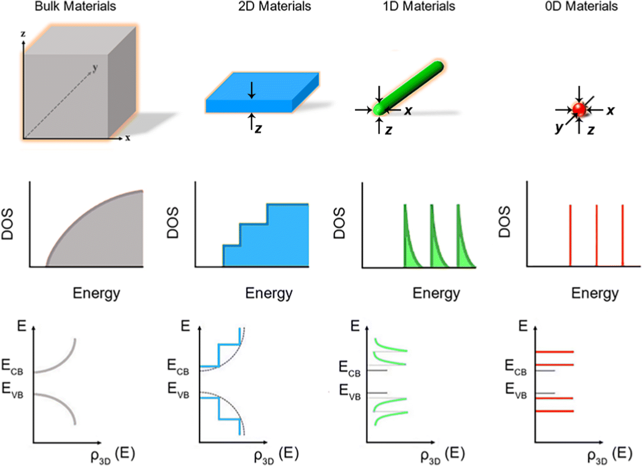 | ||
| Fig. 1 Schematic illustration of energy level structures and functional forms of the DOS in bulk, 2D, 1D and 0D materials. Reproduced from ref. 12 with permission from Royal Society of Chemistry, copyright 2012. Reproduced from ref. 13 with permission from Springer, copyright 2016. Reproduced from ref. 14 with permission from Royal Society of Chemistry, copyright 2018. | ||
2.3 Giant oscillator strength transition
Oscillator strength defines the probability of the absorption or emission transition between the ground state and excited state.84,85 2D NPLs differ from 0D QDs and 1D NRs due to their strong quantum confinement effect in the one-dimensional range.86 The extended lateral dimensions of the NPLs can give rise to an in-plane coherent and large center-of-mass motion of the exciton, i.e., the so-called GOST,87 which would typically occur with suppressed acoustic phonon scattering. Such a GOST enhances the absorption cross-section and significantly shortens the exciton radiative decay time.88Using the optical Stark effect (OSE), the oscillator strength FStark of the exciton transition can be calculated using the following formula:89
 | (2) |
 | (3) |
 | (4) |
3. Synthetic methods, growth mechanisms and morphology control
3.1 Synthesis and growth mechanisms
 | ||
| Fig. 2 (a) Schematic illustration of the hot-injection method for the synthesis of semiconductor NPLs. (b) Schematic illustration of NC nucleation and growth processes of the hot-injection method. Reproduced from ref. 97 with permission from Annual Reviews, copyright 2000. (c) Absorption and PL spectra of CdSe NPLs. (d) Transmission electron microscopic (TEM) image of CdSe NPLs. Reproduced from ref. 98 with permission from American Chemical Society, copyright 2013. (e) Schematic illustration of one-pot heating-up method for the synthesis of semiconductor NPLs. (f) Schematic illustration of NC nucleation and growth processes of the one-pot heating-up method. Reproduced from ref. 99 with permission from American Chemical Society, copyright 2008. (g) Absorption and PL spectra of CdSe nanoribbons. Inset: FWHM of the PL emission peak. (h) TEM image of CdSe nanoribbons. Inset: a high-resolution transmission electron microscopy (HRTEM) image of CdSe nanoribbons. Reproduced from ref. 2 with permission from American Chemical Society, copyright 2006. | ||
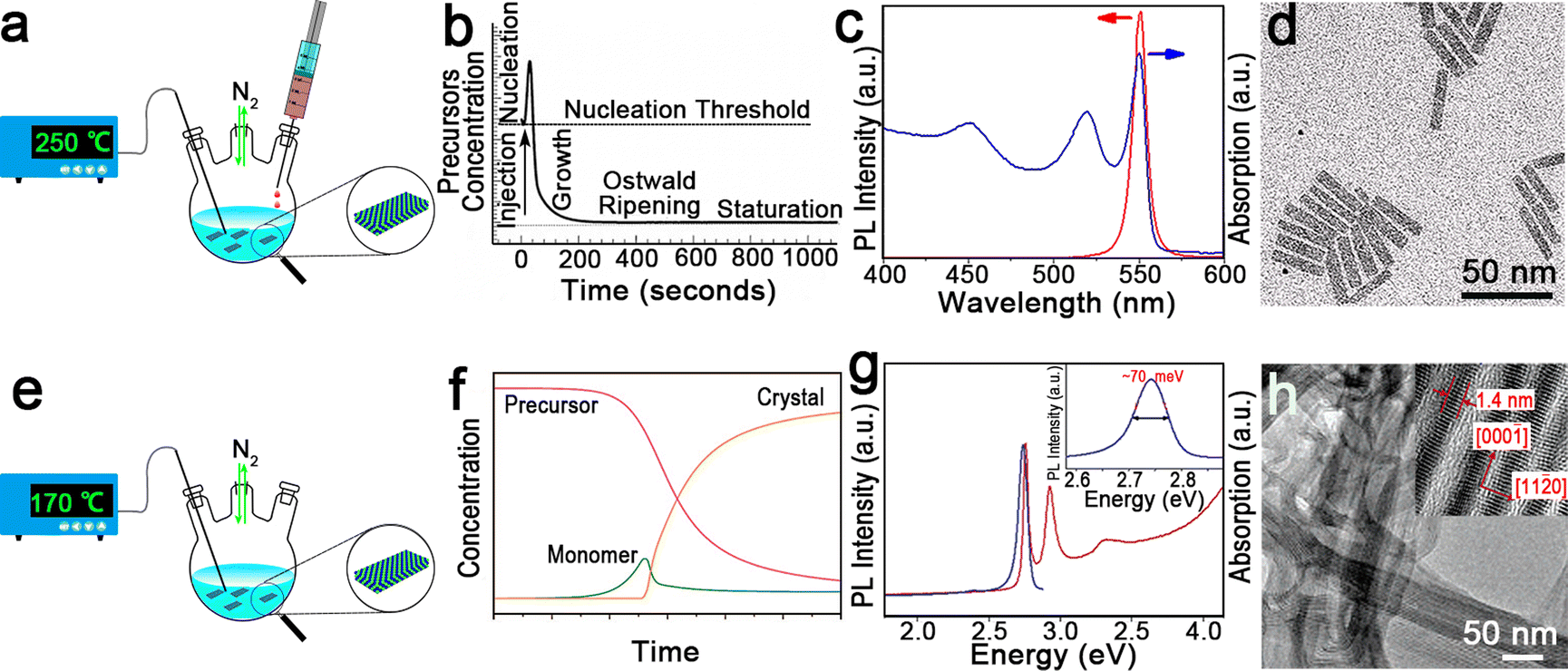
In 2008, Ithurria et al.26 utilized a modified hot-injection method to synthesize CdSe NPLs with tunable thickness. In a typical synthesis of CdSe NPLs, the metal acetate powder was added to the reaction solution after Se precursor was injected. The nucleation and lateral growth processes were separated by the addition of metal acetate. The former injection of Se precursor resulted in small CdSe crystal seeds or magic-size clusters by reacting with the Cd precursor. Subsequently CdSe crystal seeds or magic-size clusters were further laterally extended into CdSe NPLs with the assistance of acetate. The thickness and lateral size could be controlled by changing the reaction time and temperature at which metal acetate was added. The CdSe NPLs obtained by the hot-injection method possess the sharp first and second exciton peaks at 551 nm and 520 nm, respectively (Fig. 2c), and exhibit good monodispersity (Fig. 2d). Additionally, these CdSe NPLs with a PLQY of 40% have an extremely narrow emission peak at 551 nm with an FWHM of 8.5 nm (35 meV). Interestingly, the line width PL spectrum of the CdSe NPL ensemble is smaller than that of the PL spectrum (42 meV) of a single NPL, which may be caused by the existence of several emitting states in single NPL.98
In such a typical hot-injection method, acetate is necessary for the formation of NPLs because acetate can contribute to the anisotropic growth while carboxylates with long carbon chains result in isotropic growth.100 This hot-injection method has been further expanded for the preparation of CdS and CdTe NPLs.23,31,101 The NPLs obtained by the hot-injection method always possess a zinc blende structure, which is caused by the zinc blende seeds or clusters formed at the stage of the burst nucleation at a high reaction temperature. However, the synthesis of zinc blende Zn-based NPLs using this method is unsuccessful so far due to the narrow growth window parameters.
The other synthetic method is the one-pot heating-up method developed for semiconductor QDs by Hyeon et al.102 in 2001. In a typical one-pot heating-up method, all the reactants are loaded into the flask at room temperature and then the mixture is heated up to the target temperature. The nucleation and growth processes of the one-pot heating-up method are generally composed of four stages, including monomer formation, nucleation, growth and equilibrium (Fig. 2f). During the heating-up process, monomer increases as the precursor concentration decreases due to the dissolution of these precursors by ligands or the formation of free monomers. Nucleation occurs once the temperature and monomer reach the nucleation threshold, and the monomer decreases quickly in the following growth stage. Finally, the remaining precursor is depleted and the NC concentration is constant.
In 2006, Joo et al.2 utilized this method to prepare wurtzite CdSe nanoribbons for the first time. These nanoribbons can be regarded as quasi-2D NCs due to the submicrometer scale length, the tens of nanometers width and the ultra-thin thickness in the quantum confinement regime,103 exhibiting obvious one-dimensional confinement of charge carriers. In this case, a slight surface energy difference (several meV Å−2)104 between ±(1![[1 with combining macron]](https://www.rsc.org/images/entities/char_0031_0304.gif) 00) facets and ±(11
00) facets and ±(11![[2 with combining macron]](https://www.rsc.org/images/entities/char_0032_0304.gif) 0) facets, and the selective adhesion of surfactant molecules on specific facets are the key factors that affect the anisotropic growth of CdSe nanoribbons.2 However, such slight surface energy difference becomes insignificant and less determinative in affecting the growth rates of the facets at high temperature. Therefore, a low temperature of 70 °C is preferred for the synthesis of CdSe nanoribbons. The obtained CdSe nanoribbons have sharp and intense absorption peaks and an emission peak with an unprecedently narrow FWHM of 11 nm (∼70 meV) (Fig. 2g), approaching the limit of homogeneous line broadening of a single CdSe QD at room temperature.105 Additionally, the HRTEM image of CdSe nanoribbons confirms their uniform thickness (Fig. 2h).
0) facets, and the selective adhesion of surfactant molecules on specific facets are the key factors that affect the anisotropic growth of CdSe nanoribbons.2 However, such slight surface energy difference becomes insignificant and less determinative in affecting the growth rates of the facets at high temperature. Therefore, a low temperature of 70 °C is preferred for the synthesis of CdSe nanoribbons. The obtained CdSe nanoribbons have sharp and intense absorption peaks and an emission peak with an unprecedently narrow FWHM of 11 nm (∼70 meV) (Fig. 2g), approaching the limit of homogeneous line broadening of a single CdSe QD at room temperature.105 Additionally, the HRTEM image of CdSe nanoribbons confirms their uniform thickness (Fig. 2h).
Unlike the wide availability of anion precursors utilized in the synthesis of metal sulfide and selenide NCs, tellurium precursors with appropriate reactivity for the synthesis of metal telluride NPLs at low or elevated temperature are very few. It was demonstrated that the (Me2N)3P-Te precursor could facilitate the formation of 2D CdTe nanostructures at 100 °C after a long reaction time of 16 h.33 The obtained CdTe NPLs possess the wurtzite structure and sharp band edge absorption peak at 489 nm, indicating a uniform thickness of ∼1.9 nm. While a temperature of 200 °C and short reaction time (30 min) are required in the reaction system containing the tributylphosphine (TBP)-Te precursor reduced by superhydride.38,39 These wurtzite ZnTe NPLs have rectangle shape with lateral dimensions of ∼20 nm × ∼60 nm and a uniform thickness of ∼1.5 nm. Additionally, the one-pot heating-up method facilitated the formation of wurtzite ZnS34,35 and ZnSe36 NPLs with 4 ML thickness by the assistance of primary amines. The obtained Zn-based NPLs exhibit extremely narrow band edge emission FWHMs of several nanometers owing to their atomic flatness.
In addition to II–VI NPLs, Ag2S,106 PbS67 and Cu2S107 2D nanostructures can also be obtained using the one-pot heating-up method. Kubie et al.106 prepared water soluble Ag2S NPLs with uniform thickness by using 3-mercaptopropionic acid (MPA) as both sulfur source and ligand in ethylene glycol, and the obtained Ag2S NPLs possessed an ultra-thin thickness of ∼0.35 nm. Other NPLs including ultra-thin PbS nanosheets with high crystallinity were synthesized by the decomposition of Pb(SCN)2 in the presence of OAm and OA.67 The obtained PbS nanosheets possess a thickness of 1.2 nm and orthorhombic phase. However, these PbS nanosheets do not exhibit distinct excitonic absorption features, which may be attributed to the weak oscillator strengths for the lowest excited states.67
Template-assisted growth. Son et al.27 investigated the growth process of CdSe NPLs in a solution of primary amines and proposed the template-assisted growth mechanism, as depicted in Fig. 3a. In a typical synthesis, after CdCl2 was added to a mixture solution containing both octylamine and OAm, [CdCl2(octylamine,OAm)2] lamellar complexes were formed. The stacked CdSe NPLs were obtained by the selenylation of [CdCl2(octylamine,OAm)2] lamellar complexes using Se powders as selenium precursor. The rigid and bulky carbon chains of OAm weakened the attraction between the stacked NPLs, and thus, the free-standing NPLs were obtained by sonication. According to the results revealed by the first-principles method based on density functional theory (DFT),38 the growth process of these CdSe NPLs is interpreted as follows. The nonpolar ±(11
0) facets possess the lowest surface energy and serve as the dominant basal planes (top and bottom planes), which determine the final morphology of CdSe NPLs. The nonpolar (100) and (100) facets are stable and serve as the terminated facets along the [100] and [100] directions. The polar ±(0002) facets possess the highest surface energy and the growth of these facets leads to the elongation of CdSe NPLs along the [0002] direction (Fig. 3c bottom right). The obtained stacked CdSe NPLs has a thickness of 1.4 nm with atomic flatness, contributing to the extremely narrow line width of band edge emission transition (Fig. 3d). Compared to the free-standing CdSe NPLs, although the stacked CdSe NPLs exhibit a noticeable tailing in the absorption spectrum, the emission spectra of both free-standing and stacked CdSe NPLs are quite similar, as compared in Fig. 3d. The stacked NPLs were also obtained by utilizing single type of amine, for example, octylamine, as both the reaction solution and surfactant. Those stacked NPLs could be disassembled into free-standing ones by a high-temperature solvothermal process in acetone.108 In this disassembly process, the hot acetone facilitated the outward diffusion of octylamine from the interlayer spacing of stacked NPLs by dissolving octylamine.
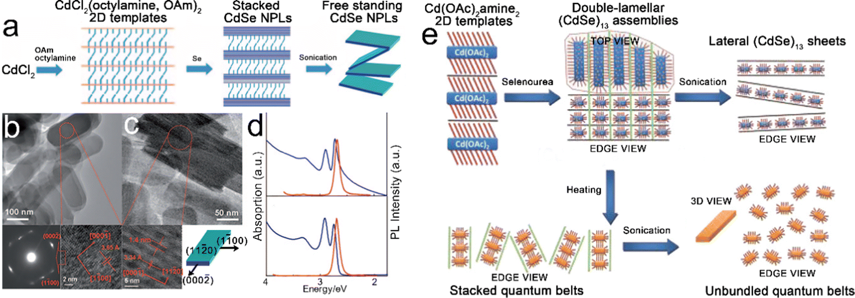 | ||
| Fig. 3 (a) Schematic illustration of the template-assisted growth of CdSe NPLs. (b) Top view TEM image, selected area electron diffraction (SEAD) pattern (bottom left) and HRTEM image (bottom right) of stacked CdSe NPLs. (c) Side view TEM image, HRTEM image (bottom left) of stacked CdSe NPLs and crystallographic structure of CdSe NPLs. (d) Absorption and PL spectra of free-standing (bottom) and stacked (top) CdSe NPLs. Reproduced from ref. 27 with permission from Wiley-VCH copyright 2009. (e) Schematic illustration of double-lamellar-template-assisted growth of CdSe quantum belts. Reproduced from ref. 30 with permission from American Chemical Society, copyright 2011. | ||
Besides the template-assisted growth mechanism, a similar growth mechanism, named double-lamellar-template-assisted growth, was proposed by Liu et al.30 to interpret the growth of CdSe quantum belts with ultra-thin thickness (Fig. 3e). The (CdSe)13 nanocluster assemblies entrained within the double-lamellar templates were formed by the exposure of lamellar [Cd(OAc)2amine2] 2D templates to selenourea at room temperature. These double-lamellar (CdSe)13 nanocluster assemblies exhibited different disassembly dimensions. For example, lateral (CdSe)13 sheets were obtained from the lateral disassembly of (CdSe)13 nanocluster assemblies by sonication, while stacked CdSe quantum belts were obtained from the vertical disassembly of (CdSe)13 nanocluster assemblies by heating. The free-standing CdSe quantum belts could be obtained by the sonication of stacked CdSe quantum belts. The PLQY of the obtained CdSe quantum belts is 42%, which is considered as the result of the low density of surface trap sites distributed primarily at the edges. Son et al.24 investigated the influences of the stability of magic-sized clusters in the template-assisted growth process of CdS nanoplates. The different stabilities of magic-size CdS clusters resulted in the selective formation of 0D, 1D and 2D CdS NCs. When the reaction was conducted at 70–100 °C in OAm solution, the magic-size CdS clusters were not stable, resulting in 0D NCs and 1D NRs. While in the solution of alkylamine with a saturated hydrocarbon chain, the magic-size CdS clusters were stable at 80 °C and produced 2D structured CdS NPLs.24
Oriented attachment. Oriented attachment refers to the spontaneous self-organization of adjacent particles. These particles share a common crystallographic orientation and can be joined at a planar interface.109 The ultra-thin single-crystal sheets with lateral dimensions of micrometer scale were obtained by the oriented attachment of PbS NCs for the first time.110 In 2011, Ithurria et al.28 demonstrated that zinc blende CdSe NPLs with atomic flatness were formed by oriented attachment. In a typical synthetic process (Fig. 4a), CdSe monomers were formed at the early stage of the reaction and were transformed into CdSe NPL seeds. The CdSe NPL seeds and/or monomers were attached two-dimensionally and extended into large CdSe NPLs. In the obtained CdSe NPLs, the top and bottom planes are perpendicular to the [001] direction. Additionally, the orientation of the NPL edges is confirmed to be perpendicular to [100] and [010] directions, respectively. This crystal orientation is surprising because all these axes are equivalent in zinc blende CdSe. Such formation process of these zinc blende CdSe NPLs suggests the symmetry is broken.28 During the extension process from CdSe NPL seeds to CdSe NPLs, the thickness is constant, which is confirmed by the unchanged absorption and PL peak positions. The obtained CdSe NPLs exhibit bright emission with a PLQY of 50%.28
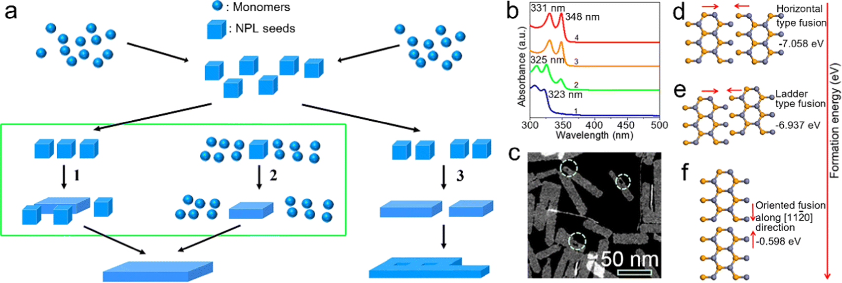 | ||
| Fig. 4 (a) Schematic illustration of the oriented attachment mechanism responsible for the formation of semiconductor NPLs. The lateral extension by oriented attachment of NPL seeds (path 1), monomers (path 2) and small NPLs (path 3). Reproduced from ref. 28 with permission from American Chemical Society, copyright 2011. (b) Absorption spectra of ZnSe NCs reacted at 150 °C after 2 minutes (1), 4 minutes (2), 30 minutes (3) and 2 hours (4). (c) High angle annular dark field scanning transmission electron microscopy (HAADF-STEM) image of ZnSe NPLs. (d) Horizontal-type oriented fusion of ZnSe NWs along the [100] direction. (e) Ladder-type oriented fusion of ZnSe NWs along the [100] direction. (f) Vertical-type oriented fusion of ZnSe NWs along the [110] direction. Reproduced from ref. 38 with permission from American Chemical Society, copyright 2019. | ||
Chen et al.111 demonstrated that zinc blende CdSe NPLs were formed by the oriented attachment of CdSe seeds, which does not involve CdSe monomers. The oriented attachment process can be divided into three stages. In the primary stage, CdSe seeds with a larger diameter than the thickness of final CdSe NPLs are transformed to single-dot intermediates with nearly flat (100) facets and similar thickness to that of the final CdSe NPLs. This transformation contributes to the slight expansion of lateral dimensions and side facets, including stable (100) and reactive (110) facets. In this stage, acetate and stearate molecules play different roles: acetate molecules accelerate this transform process, while stearate molecules preserve the good monodispersity of single-dot intermediates. In the second stage, two single-dot intermediates fuse together along the reactive side (110) facets, resulting in the formation of 2D embryos. Then, the continuous fusing process between single-dot intermediates and 2D embryos results in irregular lateral dimensions. In the last step, single-dot intermediates are further attached to the 2D embryos and other reactive 2D NCs with irregular lateral shape along (110) or other active side facets. At the same time, the resulting 2D NCs convert their side facets to (100) facets by intra-particle ripening. Ultimately, the remaining (110) and other reactive side facets of the resulting 2D NCs will gradually be eliminated through intraparticle ripening, resulting in stable CdSe NPLs with (100) side facets as the dominant surfaces.111
Besides zinc blende II–VI semiconductor NPLs, the formation of wurtzite II–VI semiconductor NPLs including ZnSe and ZnTe is also based on the oriented attachment mechanism.38 During the growth of wurtzite ZnSe NPLs, the absorption spectrum of the final ZnSe NPLs (4 in Fig. 4b) resembles that of the preceding ZnSe NPLs with a small lateral size (3 in Fig. 4b), which demonstrates that the NPLs are formed by the oriented attachment of the preceding NPLs along the lateral direction without an increase in thickness.38 Additionally, it should be noted that evidently the hollow features and patches are presented in the obtained ZnSe NPLs, which also indicate that the NPLs are formed by oriented attachment,38 in which wurtzite II–VI NPLs also involve both horizontal and vertical growth.38 Due to the low energy of horizontal-type fusion, the small ZnSe seeds with a size of 0.99 nm (6 MLs) are attached laterally along the [100] direction and bundled ZnSe NWs with a uniform width of 0.99 nm are obtained, exhibiting a band edge absorption at 323 nm (1 in Fig. 4b). As the reaction proceeds, the bundled ZnSe NWs become fused and fragmented, resulting in a slight red shift to 325 nm of band edge absorption (2 in Fig. 4b). Subsequently, the fused ZnSe NWs convert into small lateral-sized ZnSe NPLs with an obvious increase in thickness from 0.99 nm to 1.39 nm (4 MLs), which is confirmed by the apparent red shift of band edge absorption from 325 nm to 348 nm (3 in Fig. 4b). Finally, ZnSe NPLs are formed by the oriented attachment of small lateral-sized ZnSe NPLs along the [110] direction.38
Intrinsic instability induced growth. Although template-assisted growth and oriented attachment have already provided some insights into the growth processes of NPLs; further understanding of NPL growth from a perspective of formation energy is also important, especially for zinc blende Cd-based NPLs with tunable thickness and lateral size. Anisotropic NPLs possess two wide facets (top and bottom planes) and four narrow facets (sidewalls). Nucleation may occur on either the wide facets or narrow facets during the growth process, as shown in Fig. 5a. When nucleation occurs on the narrow facets before the wide facets, the anisotropic growth results in products with a 2D morphology. When nucleation occurs on both narrow and wide facets, the isotropic growth results in the products with a spherical morphology.40,61 Obviously, the formation energies of nucleation on narrow and wide facets determine the morphology of NCs. In 2017, Riedinger et al.61 demonstrated that an intrinsic instability growth mechanism resulted in such anisotropic 2D structure. In this growth mechanism, NPLs were considered as the consequence of selective lateral-extension of QDs with a diameter same as that of the thickness of NPLs. A zinc blende CdSe NC with (001) facets terminated by Cd2+ and passivated by acetates was employed as a model to investigate how the energy changes as the growth of NPLs evolves. The variation of total energy can be calculated as follows:
| ΔE = ΔV·EV + ΔA·EA + ΔL·EL, | (5) |
| Ewide(a) = (L1EV)a + (4L1EA + 2EL)a1/2 + 4L1EL, | (6) |
| Enarrow(a) = (L1EV + 2EA/w)a + 2wL12EA + (w + 4)L1EL, | (7) |
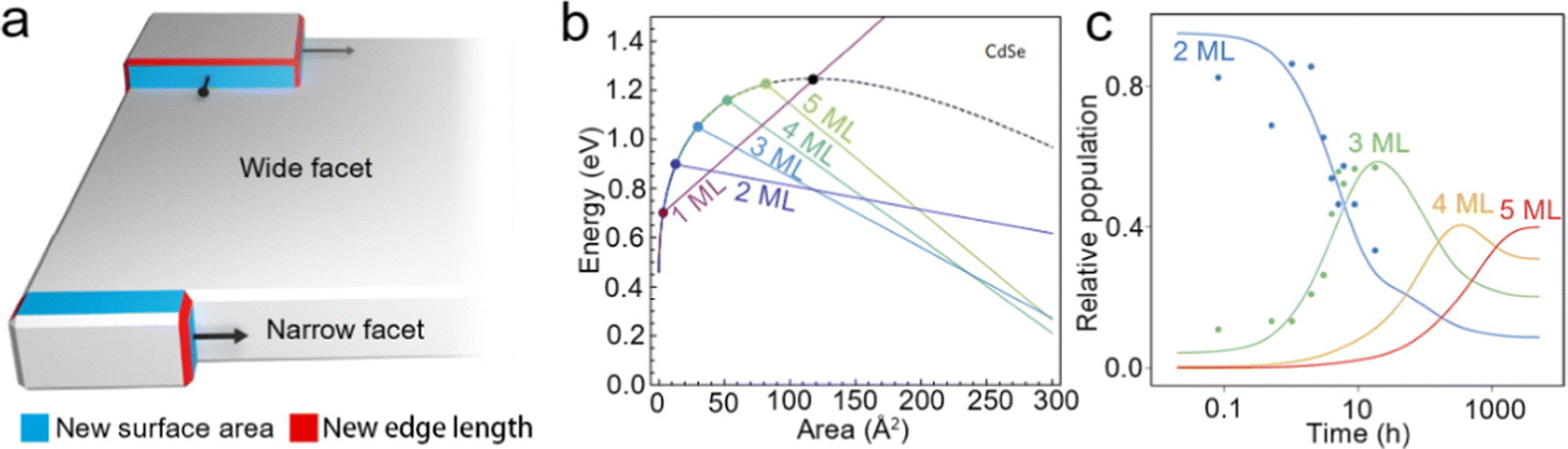 | ||
| Fig. 5 (a) Schematic illustration of intrinsic instability induced growth of semiconductor NPLs. (b) Calculated energy versus island size on wide facets (black dashed line) and narrow facets (colored lines) of different thicknesses in CdSe NPLs. (c) Experimental data for the relative populations of 2 ML, 3 ML, 4 ML and 5 ML CdSe NPLs versus growth time. Reproduced from ref. 61 with permission from Springer Nature, copyright 2017. | ||
3.2 Morphology control
Based on the establishment of synthetic methods and the growth mechanisms of NPLs, the morphology control of semiconductor NPLs in terms of thickness, lateral size and structures can be achieved and thus their optical properties can be altered. In semiconductor NPLs, the controlled thickness and lateral size and other structures caused by the morphology change, such as helical, scroll-like and long-range ordered structures, have also been investigated. In this section, we will focus on the strategies that can help in controlling the morphology of semiconductor NPLs and other complex structures induced by the change of NPL morphology.CdSe NPLs thicker than 6 MLs can be synthesized in ODE solution in the presence of chlorides.40 According to ΔE = ΔVEV + ΔAEA + ΔLEL mentioned in the intrinsic instability induced growth section, the map of synthesizability of NPLs by EL and EA at an EV of −2.2 meV Å−3 is shown in Fig. 6a, which reveals that 6 ML and 7 ML CdSe NPLs seem inaccessible. When some small anionic ligands such as chlorides are added to the reaction, EV increases from −2.2 meV Å−3 to −1.8 meV Å−3, as calculated by the enthalpies of CdSe obtained from different Cd precursors, such as Cd(OAc)2 and CdCl2. This EV difference of 0.4 meV Å−3 equals to 2 kJ mol−1 for zinc blende CdSe and is sufficient to change the nucleation barrier, facilitating the lateral extension of 6 ML CdSe NPLs. A new map of synthesizability of NPLs by EL and EA at an EV of −1.8 meV Å−3 is shown in Fig. 6b, which indicates that it is possible to form 6 ML CdSe NPLs, as confirmed by the sharp emission peak at 586 nm which can be assigned to 6 ML CdSe NPLs.
 | ||
| Fig. 6 Synthesizability of semiconductor NPLs by EL and EA at an EV of −2.2 meV Å−3 (a) and an EV of −1.8 meV Å−3 (b), red circle is the point with EA = 5.7 meV Å−2 and EL = 37.1 meV Å−1. Reproduced from ref. 40 with permission from American Chemical Society, copyright 2018. (c) Schematic illustration of the synthesis process of CdSe NPLs with different thicknesses (4.5–8.5 MLs). (d) Digital picture of CdSe NPLs with different thicknesses under ultraviolet (UV) illumination. Reproduced from ref. 41 with permission from American Chemical Society, copyright 2018. (e) Formation energies of diffusion and nuclei construction along the [110] direction for three additional layers. Reproduced from ref. 38 with permission from American Chemical Society, copyright 2019. | ||
Chlorides can also be utilized to tune the thickness of CdSe NPLs from 4.5 to 8.5 MLs through an Ostwald ripening process. Christodoulou et al.41 developed a two-step approach to synthesize CdSe NPLs with the assistance of chlorides. 4.5 ML CdSe NPLs were prepared using a traditional protocol at 115–220 °C in the first step and thick CdSe NPLs were obtained in the second step by adding a mixture of CdCl2, CdO and OA at 280–320 °C (Fig. 6c). The thickness growth from 4.5 ML NPLs to thick ones was achieved by an Ostwald ripening process. Chlorides may modify the surface energy and reduce the nucleation barriers for CdSe islands on the top and bottom planes, facilitating a fast transversal extension and more isotropic growth. Therefore, thick NPLs possessed a larger lateral size than that of 4.5 ML ones and the thickness of NPLs increased continuously by a layer-by-layer mode in this Ostwald ripening process. The obtained CdSe NPLs with 8.5 MLs possess a sharp emission peak at 625 nm, which is the longest emission wavelength for core-only CdSe NPLs. It should be noted that some slight satellite peaks exist at the blue and red sides of the main emission peak, which are caused by the small heterogeneous thickness broadening within 1 ML. Moghaddam et al.116 proposed a dissolution-recrystallization process that could increase the thickness of NPLs with the assistance of halides. Halides assist the dissolution of CdSe NPLs from the sidewalls into the solution. The released monomers prefer to be deposited on both the top and bottom planes instead of sidewalls. The largest percentage of the available top and bottom planes and the competition of dissolution and recrystallization processes can account for this phenomenon. The obtained thick NPLs possess smaller lateral size than the starting NPLs and the thickness of NPLs increases in steps of 2 MLs, which are different from the ripening process. Additionally, subnanometer thick CdSe NPLs were obtained as well by the reaction of cadmium acetate and TOP-Se in the mixture of OA and trioctylamine at an elevated temperature of 120 °C.42 These CdSe NPLs possess a high PLQY of 90% and a broad emission peak covering the visible region due to the presence of the surface traps. These CdSe NPLs exhibit significantly larger absorption cross-section compared to thicker CdSe NPLs (>1 nm), which is attributed to the manifestation of giant oscillator strength.42
Except for zinc blende CdSe NPLs, studies on the thickness control of wurtzite 2D CdSe NCs have also been conducted as well. In the synthesis of CdSe quantum belts, by the reaction of Cd(OAc)2(octylamine)x and selenourea, a low reaction temperature (45–80 °C) led to the formation of thin wurtzite CdSe quantum belts with the first exciton peak at ∼485 nm, while an elevated reaction temperature of ∼120 °C produced thick wurtzite CdSe quantum belts with the first exciton peak at ∼518 nm. Such red shift of the first exciton peak position from 485 nm to 518 nm indicated a clear increase in the thickness of quantum belts.30 However, most wurtzite NPLs possess a constant thickness of 4 MLs and to date wurtzite NPLs with a thickness larger than 4 MLs have not been reported. Pang et al.38 employed the first-principles methods based on DFT to investigate the growth kinetics of wurtzite ZnSe NPLs, in particular to elucidate why wurtzite NPLs exhibited the unique thickness of 4 MLs (Fig. 6e). The formation energies of diffusion and nuclei construction along the [110] direction for three additional layers on the ZnSe NWs with a diameter of ∼0.99 nm are shown in Fig. 6e. A small energy barrier of 0.0359 eV (equivalent to 415 K) is required to overcome to enable the deposition of the first additional layer along the [110] direction, and this is accessible with the thermal energy of the reaction system (150 °C, 423.15 K). The deposition of the second additional layer is spontaneous because the formation energy is negative. However, the formation energy for the deposition of the third additional layer along the [110] direction increases to 0.0654 eV (equivalent to 760 K), which is out of the scope of the experimental conditions for colloidal synthesis. This explains why such wurtzite NPLs generally have a unique thickness of 4 MLs.38 It should be noted that the calculations were conducted by assuming that the growth of wurtzite NPLs was conducted in methylamine, but these reactions were carried out in oleylamine. Compared with oleylamine which has a long carbon chain of 18 carbon atoms, methylamine is much shorter and has much higher binding energy to the surface atoms of wurtzite II–VI semiconductor NPLs. Such a large difference in the binding capability of the surfactants between methylamine and oleylamine is likely to increase the formation energy (barrier energy for the growth of an additional layer on the existing NPLs) obtained by density functional theory simulations.
From the above discussions, it is interesting to see that the thickness control of zinc blende semiconductor NPLs such as CdSe has been achieved while that of wurtzite semiconductor NPLs is inaccessible. A close inspection into the surface structures of these NPLs can provide some insights into the origins of such differences. For zinc blende CdSe NPLs, their top and bottom basal planes are polar surfaces terminated by Cd2+.117 These Cd2+ are positively charged and possess strong affinity to negatively charged Se2−, facilitating the alternative deposition of Se2− followed by the deposition of Cd2+, which leads to thick zinc blende CdSe NPLs. However, for the wurtzite ZnSe NPLs, both top and bottom basal planes are nonpolar surfaces and terminated by the same amounts of cations and anions.118 Therefore, the affinity of extra ions, either Cd2+or Se2−, to such neutral surfaces of wurtzite CdSe NPLs is much weaker than that to polar surfaces of zinc blende CdSe NPLs. This likely makes it difficult to achieve thick (>4 MLs) wurtzite NPLs by depositing extra cations and anions on both top and bottom planes.
Besides traditional semiconductor NPLs, thickness control of metal halide perovskite NPLs has also been demonstrated recently.119–128 Metal halide perovskites can be described as L2[ABX3]n−1BX4, where L represents long-chain organic ligands, A represents monovalent metal or organic cations, B represents divalent metal cations, X represents halide anions and n is the number of perovskite unit cells.129 Perovskite NPLs with single unit cell thickness were separated for the first time by purification from the reaction products of colloidal perovskite NCs.130 The obtained methylammonium lead bromide (MAPbBr3) NPLs with single unit cell thickness exhibited a sharp absorption peak with an obvious 0.5 eV blue shift from that of the bulk perovskite phase, resulting from the quantum confinement effect of perovskite NPLs.130
In 2015, Sichert et al.131 developed a direct synthetic method to prepare perovskite NPLs. The long-chain organic molecule of octylammonium and the short-chain organic molecule of MA were mixed and utilized to control the thickness of MAPbBr3 NPLs by changing the ratio of octylammonium and MA. As the content of octylammonium increased, the thickness of the obtained NPLs decreased, resulting in the enhancement of the quantum confinement effect (Fig. 7a). When the content of octylammonium was 100%, perovskite NPLs possessed a thickness same as that of 1 ML PbBr6 octahedron, which was similar to that of layered perovskite NCs reported previously.131 It was found that in thin NPLs with a thickness of ≤2MLs, the exciton binding energy increased to an order of several hundreds of meV, which partially counteracted the blue shift caused by the quantum confinement effect.131 Later that year, Bekenstein et al.133 achieved inorganic cesium lead halide (CsPbBr3) perovskite NPLs by lowering the reaction temperature of the synthesis method for perovskite NCs. A reaction high temperature between 140 °C and 200 °C resulted in 0D CsPbBr3 NCs, while a low temperature between 90 °C and 130 °C resulted in 2D CsPbBr3 NPLs. When the reaction was conducted at 90–100 °C, the obtained CsPbBr3 NPLs possessed lamellar structures ranging from 200–300 nm in length, indicating that the organic mesostructures served as growth directing templates that broke the inherent symmetry and resulted in lateral extension. Except for the reaction temperature, Pan et al.132 demonstrated that the amines with short carbon chains also played a key role in the formation of 2D NPLs. Ligands passivated on the particular facets and decreased the surface energy, resulting in anisotropic shapes by lowering the growth rates of these facets. For NPLs, amines competed with Cs+ on the surface of the growing NPLs and selectively slowed the growth rate along the orthogonal direction. The amines with shorter carbon chains diffused faster than amines with longer carbon chains, resulting in more pronounced shape anisotropy and thinner NPLs (Fig. 7b).132
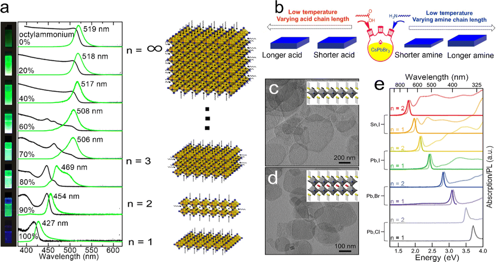 | ||
| Fig. 7 (a) Absorption and PL spectra of MAPbBr3 NPLs with different thicknesses. Reproduced from ref. 131 with permission from American Chemical Society, copyright 2015. (b) Summary of the thickness dependence on the chain length of carboxylic acids and amines. Reproduced from ref. 132 with permission from American Chemical Society, copyright 2016. TEM images of L2[ABX3]n−1BX4 NPLs, (c) n = 1 and (d) n = 2. (e) Absorption and PL spectra of L2[ABX3]n−1BX4 NPLs with different thicknesses and halides. Reproduced from ref. 129 with permission from American Chemical Society, copyright 2016. | ||
Weidman et al.129 reported that the emission peaks of perovskite NPLs could be continuously tuned in the visible region by controlling their thickness and composition. Due to the quantum confinement effect, a blue shift of 0.6 eV of band edge absorption could be achieved in perovskite NPLs. The variation of divalent metal cations (B) and halide anions (X) provided huge potential for the control of absorption and emission wavelengths (Fig. 7e). The species of monovalent metal cations (A) can influence both the optical properties and stability of perovskite NPLs. As the size of the monovalent cations increases from Cs to formamidinium, the absorption peak shifts by about 20 meV to the low energy region accompanied by a narrow absorption and emission line width. The formamidinium can improve the PLQY and a high PLQY of 88% in formamdinium-based perovskites with few monolayers was achieved.134
Besides the direct synthesis from precursors, perovskite NPLs can be obtained by the assembly of 1D or 0D NCs. For example, in 2018, Li et al.135 presented a general strategy containing a two-step process for the synthesis of CsPbX3 NPLs by the assembly of NRs. The obtained CsPbX3 NPLs possessed tunable thickness ranging from 3 nm to 6 nm and tunable lateral size ranging from 100 nm to 1 μm. In the first step, CsPbX3 NRs were prepared by the reaction of PbX2 and the mixture of long-chain (OA and OAm) and short-chain (octanoic acid and octylamine) ligands. In the second step, the CsPbX3 NPLs or nanosheets were obtained by the assembly of the NRs under the solvothermal conditions. With the assistance of additional Fe3+, perovskite NPLs could be obtained by the self-assembly of perovskite nanocubes.122 Fe3+ facilitated the protonation of OAm, which preferred to be coordinated to the given plane by substituting Cs+. Due to the passivation of OAm, further growth of perovskite nanocubes along the direction perpendicular to the plane was prevented, resulting in 2D NPLs.
Although the thickness control from 1 ML to bulk size of perovskite NPLs was achieved and the layer-by-layer growth mode of perovskite NPLs was also indicated by the discrete emission positions, it is not clear whether these perovskite NPLs have atomically flat surface and atomically precise thickness as that of CdSe NPLs. Further efforts should be devoted in elucidating the surface flatness profile and thickness of perovskite NPLs.
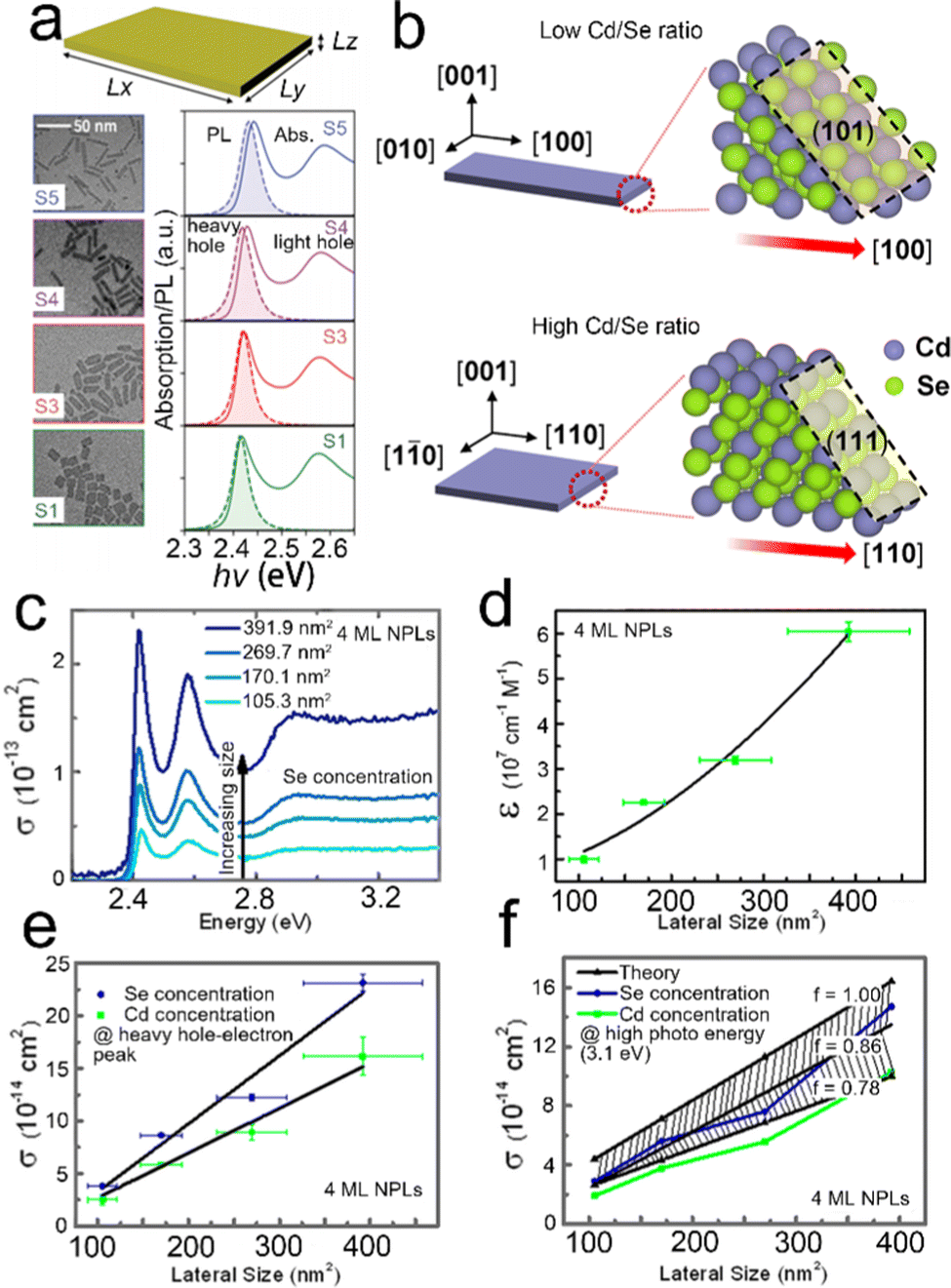 | ||
| Fig. 8 (a) TEM images, absorption and PL spectra of CdSe NPLs with different lateral sizes. Reproduced from ref. 138 with permission from American Physical Society, copyright 2020. (b) Schematic illustration of the Cd/Se ratio dependent growth direction of CdSe NPLs. Reproduced from ref. 139 with permission from American Chemical Society, copyright 2021. Absorption cross-section spectra (c) and lateral size dependent extinction coefficient (d) of 4 ML CdSe NPLs with different lateral sizes. Lateral size dependent absorption cross-section at the energy of heavy hole–electron transition peak (e) and at high photon energy of 3.1 eV (f). Reproduced from ref. 137 with permission from American Chemical Society, copyright 2015. | ||
In 2013, Bouet et al.101 achieved the controllable and continuous lateral extension of CdSe NPLs, which made it possible to produce CdSe nanosheets with well-defined thickness and a large lateral dimension of 700 nm. In a typical synthetic process, after cadmium and selenium precursors were injected, the monomer concentration reached the nucleation limit and then small CdSe NPLs were formed quickly. After the nucleation stage, the monomer concentration decreased and additional precursors were added continuously to extend the lateral size of CdSe NPLs. In the extension process involving TOP-Se, both facets parallel to (110) and (100) planes grew simultaneously. Although these facets had comparable stability, (100) facets possessed a slightly higher stability under these reaction conditions. Therefore, (100) facets became the only facets when more TOP-Se was induced.101 On the contrary, as ODE-Se was utilized, the facets of nanosheets were only parallel to the [110] direction and the most stable facets were formed containing a mixture of Cd and Se atoms. In the continuous extension process, the thickness of CdSe nanosheets was kept constant and thick CdSe nanosheets with a large lateral size were obtained by injecting the precursor into a solution containing thick CdSe NPLs.101
In terms of lateral size control, both the aspect ratio and the width of semiconductor NPLs can be controlled simultaneously. Bertrand et al.140 achieved the controllable aspect ratio and width of CdSe NPLs by introducing OH− molecules into the lateral extension process of NPLs. These OH− molecules adsorbed on the surfaces of NPLs and altered the surface energy balance, resulting in different lateral shapes of NPLs.140 The aspect ratio of NPLs was tuned from 1![[thin space (1/6-em)]](https://www.rsc.org/images/entities/char_2009.gif) :1 of a square to 8:1 of a rectangle by changing the ratio of Cd(OAc)2 and Cd(OAc)2·2H2O from 3:7 to 10:0. Meanwhile, the width of NPLs was tuned from 5 nm to 15 nm by changing the ratio of Cd(OAc)2 and Cd(OAc)2·2H2O from 9:1 to 3:7, resulting in slight red shifts of both absorption and emission peaks. A similar phenomenon was also observed by another group.138 As shown in Fig. 8a, despite the weak quantum confinement on the lateral dimension, the variation of lateral size affects the exciton and emission peaks slightly.138 Specially, as the aspect ratio decreases, red shifts in both absorption and emission spectra are observed, alongside a slight decrease of the PL line width, a decrease of the Stokes shift and an increase of the symmetry of heavy hole exciton peak. Considering the relatively weak confinement on the lateral dimension, such effects on the absorption and emission energy originate from the quantized exciton center-of-mass motion.138 Besides, the ratio of Cd and Se precursors can control the aspect ratio of CdSe NPLs as well.139 As shown in Fig. 8b, the low Cd/Se ratio contributes to a rectangular shape, in which the long edge grows fast along the [100] direction, while a high Cd/Se ratio facilitates the square shape, in which the growth of the long edge along the [100] direction is slowed down and the growth direction changes from [100] to [110]. Cd(OAc)2 adsorption is an energetically unfavorable growth for (101) and (111) surfaces at low Se and high Se coverages, respectively, which can account for the observation mentioned above.
:1 of a square to 8:1 of a rectangle by changing the ratio of Cd(OAc)2 and Cd(OAc)2·2H2O from 3:7 to 10:0. Meanwhile, the width of NPLs was tuned from 5 nm to 15 nm by changing the ratio of Cd(OAc)2 and Cd(OAc)2·2H2O from 9:1 to 3:7, resulting in slight red shifts of both absorption and emission peaks. A similar phenomenon was also observed by another group.138 As shown in Fig. 8a, despite the weak quantum confinement on the lateral dimension, the variation of lateral size affects the exciton and emission peaks slightly.138 Specially, as the aspect ratio decreases, red shifts in both absorption and emission spectra are observed, alongside a slight decrease of the PL line width, a decrease of the Stokes shift and an increase of the symmetry of heavy hole exciton peak. Considering the relatively weak confinement on the lateral dimension, such effects on the absorption and emission energy originate from the quantized exciton center-of-mass motion.138 Besides, the ratio of Cd and Se precursors can control the aspect ratio of CdSe NPLs as well.139 As shown in Fig. 8b, the low Cd/Se ratio contributes to a rectangular shape, in which the long edge grows fast along the [100] direction, while a high Cd/Se ratio facilitates the square shape, in which the growth of the long edge along the [100] direction is slowed down and the growth direction changes from [100] to [110]. Cd(OAc)2 adsorption is an energetically unfavorable growth for (101) and (111) surfaces at low Se and high Se coverages, respectively, which can account for the observation mentioned above.
The absorption cross-section and molar extinction coefficients strongly depend on the lateral size of semiconductor NPLs.137 As the lateral size increases, the extinction coefficient and absorption cross-section are improved (Fig. 8c–f). The relation between the lateral size of 4 ML CdSe NPLs and molar extinction coefficient can be summarized as the following equation:
| ε = 6130012 ± 2846504 + 1861 ± 170(LS)1.72, | (8) |
 | (9) |
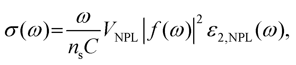
To improve the PLQY of Mn2+ doped NPLs, Davis et al.141 utilized an epitaxial growth approach to deposit a ZnS passivation layer over CdS NPLs to suppress surface defects. In Mn2+ doped CdS NPLs, although the final structure was confirmed by electron paramagnetic resonance, the dopant emission was not observed regardless of Mn2+ doping concentration. The ZnS shell eliminated the surface defect states of Mn2+ doped CdS NPLs, so the Mn2+ dopant emission emerged and its intensity was tunable as well as that of band edge emission (Fig. 9a). Additionally, the PL lifetime could be controlled by changing the dopant concentration. As the Mn2+ dopant concentration increased, the lifetimes of both band edge emission and dopant emission decreased due to the increased rate of host–dopant energy transfer and the concentration quenching from short-range Mn–Mn interactions at a high doping concentration. Although the surface of NPLs was passivated by the ZnS shell, the total PLQY of these doped NPLs was still low (15%).
 | ||
| Fig. 9 (a) Schematic illustration of energy level structures of Mn2+ doped CdS and Mn2+ doped CdS/ZnS core/shell NPLs. (b) PL lifetime of Mn2+ doped CdS/ZnS core/shell NPLs as a function of Mn2+ concentration. Inset: the average lifetimes of the NPLs as a function of Mn2+ concentration. Reproduced from ref. 141 with permission from American Chemical Society, copyright 2019. (c) PL spectra of Cu+ (top) and Cu2+ (bottom) doped 4 ML CdSe NPLs. Adopted from ref. 142 with permission from Wiley-VCH copyright, copyright 2017. Reproduced from ref. 59 with permission from American Chemical Society, copyright 2022. (d) Recombination processes of Cu+ (top) and Cu2+ (bottom) doped NCs. Reproduced from ref. 143 with permission from American Chemical Society, copyright 2011. | ||
Sharma et al.142 prepared Cu+ doped 4 ML CdSe NPLs with near-unity PLQY (97%) of dopant emission by nucleation doping strategy despite the utilization of Cu2+ as a dopant precursor. The oxidation state of Cu dopant in NPLs was +1, which may be caused by the reduction effect of TOP. The obtained Cu+ doped 4 ML CdSe NPLs exhibited a broad dopant emission larger than 700 nm (Fig. 9c top) and were utilized in luminescent solar concentrators due to the large Stokes shift. However, as the CdS shell was deposited on these Cu+ doped CdSe NPLs, the Cu+ dopant emission intensity dropped significantly and the band edge emission recovered gradually. Such observation was reported in the previous literatures and might be caused by the out-diffusion of Cu+ dopant.151,152 The combination of Cu+ dopant emission and band edge emission covered a wide range from the visible region to the near-infrared region (NIR).142 Additionally, Medda et al.59 prepared Cu2+ doped 4 ML CdSe NPLs by utilizing Cu2+ as a dopant precursor without TOP using a nucleation doping strategy. Cu2+ doped 4 ML CdSe NPLs possessed a broad dopant emission, exhibiting an obvious blue shift compared to Cu+ doped 4 ML CdSe NPLs (Fig. 9c bottom). The change in the peak position of the dopant emission may be caused by the different positions of Cu+ and Cu2+ doping energy levels. The doping species of Cu+ and Cu2+ have different recombination processes.143 As the oxidation state was +1, Cu+ accepted the holes from the valence band and recombined with excited electrons from the conduction band (Fig. 9d top). As the oxidation state was +2, Cu2+ recombined with the excited electrons from the conduction band directly without accepting the holes from the valence band (Fig. 9d bottom).
Ag+ dopants were also introduced into 4 ML CdSe NPLs by the nucleation doping strategy. Ag+ doped CdSe NPLs possessed PLQYs ranging from 50% to 80% and a Stokes shift of 90 nm.153 Furthermore, such doped CdSe NPLs exhibited light-induced magnetism. As Ag+ doped CdSe NPLs were irradiated, electrons were excited to the conduction band from the valence band and the holes formed in the valence band. After a fraction of the excited electrons were trapped by the surface defects, the holes facilitated the transform of the nonmagnetic Ag+ 4d10 state to the magnetic Ag2+ 4d9 state. The electron and hole spins were partially aligned by the sp-d exchange interaction with Ag2+ spins and the circularly polarized PL was formed by the recombination of electrons and holes.153
Besides the nucleation doping strategy, the dopants can be introduced into the host NCs during the growth process of host NCs, which was known as the growth doping strategy as demonstrated in Hg2+ doped CdSe NPLs.154 In the lateral extension processes of 4 ML CdSe NPLs at 200 °C and 240 °C, Hg(OAc)2 was added along with the addition of Cd and Se precursors. The injection temperatures of Hg dopants played a key role in the incorporation of dopants. The mild injection temperature of 200 °C resulted in both interstitial and substitutional incorporation of Hg2+ in CdSe NPLs. Hg2+ doped CdSe NPLs obtained at 200 °C exhibited a PLQY of 9% over the whole spectral region and possessed two dopant PL peaks located at 638 nm and 778 nm with large Stokes shifts and large FWHMs of 76 nm and 101 nm, respectively. While a high injection temperature of 240 °C led to the substitutional incorporation of Hg2+ in CdSe NPLs. Hg2+ doped CdSe NPLs obtained at 240 °C exhibited an enhanced PLQY of 24% and possessed only one dopant emission peak located at 615 nm with an FWHM of 53 nm.154
Recently, cation exchange strategy was utilized to prepare doped NPLs as well.153,155,156 In a cation exchange process, the dopants are added to the solution of host NCs and will enter the interior of host NCs by exchanging the cations of host NCs. Due to the preservation of the anion skeleton, the morphology of NCs will not be altered after cation exchange.148 Therefore, the post-synthesis cation exchange strategy is suitable for preparing doped 2D NCs. Khan et al.155 demonstrated that Ag+ doped 4.5 ML CdSe NPLs were obtained when a AgOAc solution was added to CdSe NPL solution in an ice bath. Ag+ dopant served as an acceptor and enabled the tunable emissions from 609 nm to 808 nm by changing the doping concentration from 0.6% to 8.8%, resulting in the PLQYs of 45–63% and a large Stokes shift (1.03 eV) that may be caused by the modifications of the local crystal field or the formation of small Ag2Se clusters under a dopant concentration (8.8%).155 Cu+ doped 4 ML CdSe NPLs were also obtained by cation exchange strategy. Typically, Cu-TOP mixed solution was added to the CdSe NPL solution at 60 °C. TOP reduced the reactivity of dopants (Cu+), avoiding full conversion from CdSe to Cu2Se.156 The obtained Cu+ doped 4 ML CdSe NPLs possessed a PLQY of 63% and a broad dopant emission accompanied by a narrow band edge emission.156
Recently, the doping structure has also been achieved in perovskite NPLs. The bond-energy mismatch between Pb–X and Mn–X (EPb–X < EMn–X) resulted in less efficient doping.157 The post-synthesis strategy was employed to achieve doping structure in perovskite NPLs. For example, Li et al.158 achieved Mn2+ doped CsPbCl3 NPLs by a post-synthetic solvothermal process, in which Mn2+ lightly doped CsPbCl3 NPLs grew into Mn2+ highly doped CsPbCl3 NPLs. The pressure was believed to accelerate the rate of dopant diffusion, adsorption and incorporation into perovskite NPLs, resulting in a high Mn2+ doping concentration of 16.8% and even the formation of CsMnCl3 NPLs. The obtained Mn2+ doped CsPbCl3 NPLs possessed a PLQY of 21% and dual emissions consisted of blue band edge emission and orange dopant emission.158 Wu et al.159 prepared Mn2+ doped perovskite NPLs by a post-synthesis strategy in immiscible bi-phase solutions without any heating. Typically, MnBr2 was dissolved in water and was extracted with hexane with the assistance of OAm, following mixing with CsPbBr3 NPL solution with stirring for 17 days. The obtained Mn2+ doped CsPbBr3 NPLs possessed a doping concentration of 8% and exhibited a PLQY of 23%. OAm served as a shuttle to transport MnBr2 through the interfaces between water and hexane and delivered MnBr2 into perovskite NPLs. Additionally, Br− could maintain an appropriate radius of Mn2+, resulting in the octahedral factor for the perovskite crystal structure.159
 | ||
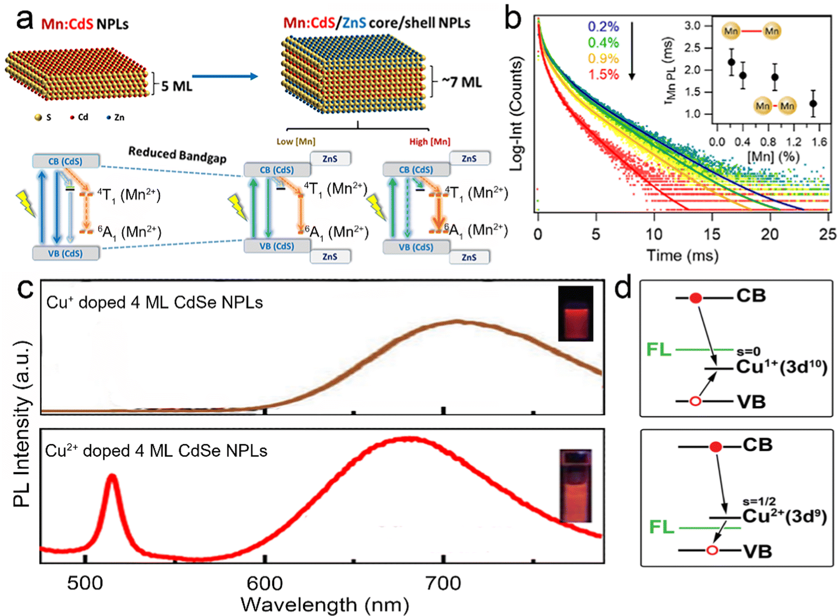
| Fig. 10 Schematic illustration of (a) PL and (b) energy levels of CdSxSe1−x alloyed NPLs in the presence of CdSySe1−y local composition fluctuations acting as a trap for the recombination process. Reproduced from ref. 160 with permission from American Chemical Society, copyright 2017. | ||
0] direction (Fig. 11b). In order to release the stress, the helical structures formed by folding the NPLs (Fig. 11c).162 Despite the observation of the helical nanostructure, it is important to identify whether such a structure is the natural state due to the drying process or the interaction caused by the TEM support grid substrate. Hutter et al.163 demonstrated that the helical morphology of CdSe NPLs was the natural state of the suspended NPLs by utilizing cryo-TEM. Furthermore, they found that a silica shell was formed by the fast incorporation between CdSe NPLs and silica. This rigid silica shell acted as a mechanical barrier against morphological changes of NPLs, which provided the opportunity for the further investigation of the helical CdSe NPL structure by HAADF-STEM (Fig. 11d), and therefore the 3D tomographic rendering of CdSe NPLs (Fig. 11e) was achieved. The helical CdSe NPLs were formed by curling NPLs along the [110] zone axis. Considering that this axis had a 45° angle with the [100] and [010] axes, the rectangle CdSe NPLs preferred to be folded into helical morphology and the square CdSe NPLs preferred to be folded into an envelope-like structure.
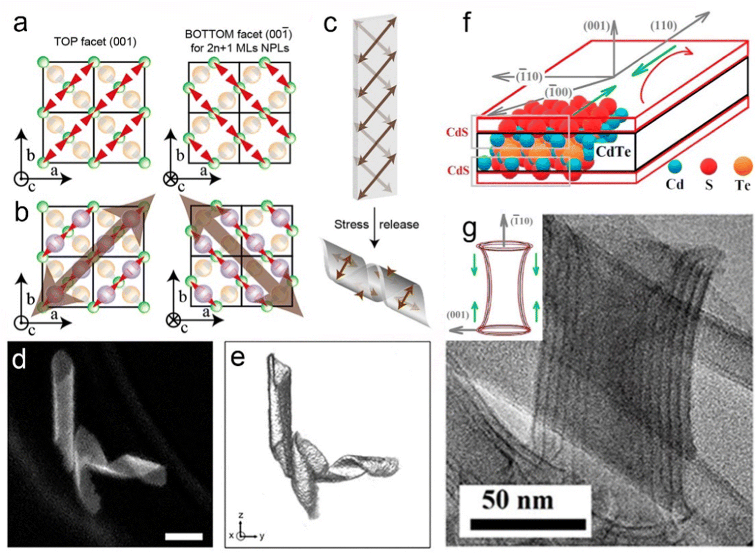 | ||
| Fig. 11 (a) Cd2+ environments of top and bottom facets in a 3 ML CdSe NPL. The red triangles represent dangling bonds, the orange atoms are Se2− and the green ones represent Cd2+. (b) Directions of stress on the top and bottom facets in a 3 ML CdSe NPL. (c) Scheme illustration of an NPL that folds as a helix for stress release. Reproduced from ref. 162 with permission from American Chemical Society, copyright 2019. (d) HAADF-STEM image and (e) 3D tomographic rendering of silica-coated helical CdSe NPLs. Reproduced from ref. 163 with permission from American Chemical Society, copyright 2014. (f) Compressive strain directions of flat NPLs. (g) TEM image of a curved NPL. Inset: compressive strain directions of curved NPLs. Reproduced from ref. 32 with permission from American Chemical Society, copyright 2018. | ||
In order to achieve the controlled assembly of NPLs, various strategies were explored. Ethanol is an antisolvent for the surface ligands and has been employed to achieve the stacked structure of NPLs by minimizing the surface energy.167,168 In this case, the NPLs are stacked on each other to maximize the contact surface between the ligands, resulting in micrometer long anisotropic needle-like superparticles.167 Upon deposition on the substrate, the superparticles exhibit polarized emission because the NPLs are oriented perpendicular to the long axis of the needles.167
Antanovich et al.169 employed another protocol to achieve stacked NPLs by utilizing the ligands. The alkyl chains in ligands could be regarded as “rigid brushes”. The formation of stacked NPLs was derived from the van der Waals interaction of “rigid brushes” between ligands of neighboring NPLs. The ligand exchange from OA with curved alkyl chain to the ligand with straight saturated chain could induce a relatively strong van der Waals interaction, resulting in the fast formation of stacked NPLs. Conversely, as OA with curved alkyl chain was exchanged by a short acetate ligand, stable colloidal NPLs were obtained because the repulsive steric potentials overweighted the van der Waals interaction.169 Carboxylic acid-terminated polystyrene was also demonstrated as beneficial for the colloidal stability of NPLs because polystyrene caused strong repulsion between neighboring NPLs.170
Although some progress has been achieved in the assembly of stacked NPLs, a mixture of nonstacked and stacked structures still existed in NPL ensembles. In 2019, Erdem et al.164 developed a liquid–air interface self-assembly technique to achieve a large-area (tens of square centimeters) CdSe NPL monolayer with uniform surface coverage on the substrate. Polar solvents with high density, which ensured the immiscibility with the nonpolar solvents of NPL solutions, were employed for the assembly of NPLs. In this process, silicon wafers with 25 nm thick Al2O3 films deposited on their top surface were used as the substrates and were immersed into polar solvents. Subsequently, NPL solution was dropped on the polar solvent and spread around the interfaces of between polar and nonpolar solvents. A uniform NPL membrane was formed after the nonpolar solvent was evaporated. The assembled CdSe NPLs were deposited on the substrates by slowly draining the polar solvents, as shown in Fig. 12a. The polar solvents played a key role in governing the orientation of NPLs. For example, the utilization of acetonitrile produced nonstacked CdSe NPLs, while the utilization of ethylene glycol resulted in stacked CdSe NPLs.164 Such different orientations might be caused by the different surface tensions and polarities of polar solvents. Momper et al.171 demonstrated that the controllable self-assembly of NPLs could be achieved at liquid–liquid interfaces by changing the evaporation rate of nonpolar solvents. As the nonpolar solvents were evaporated slowly, NPLs had enough time to be assembled and formed a stacked structure on the substrates. However, as the nonpolar solvents were evaporated quickly, the NPLs preferred to form nonstacked structure. Therefore, by changing evaporation temperature, various nonpolar solvents such as hexane, octane, and heptane could be employed in this liquid–liquid interface self-assembly technique.171
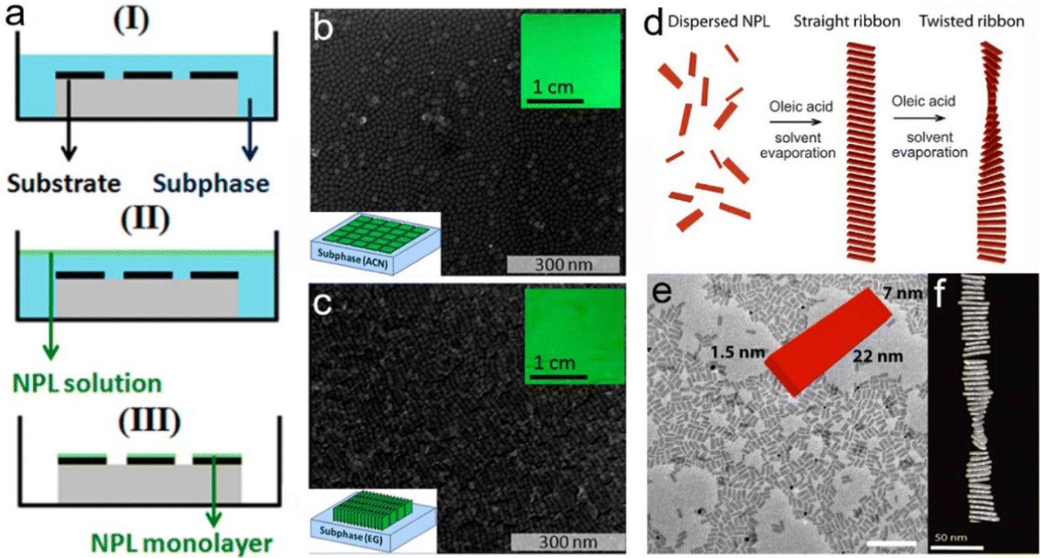 | ||
| Fig. 12 (a) Schematic illustration of the self-assembly process of semiconductor NPLs. Scanning electron microscopy (SEM) images of nonstacked NPLs (b) and stacked NPLs (c). Reproduced from ref. 164 with permission from American Chemical Society, copyright 2019. (d) Schematic illustration of the formation process of chiral ribbon. TEM images of CdSe NPLs (e) and chiral ribbon (f). Reproduced from ref. 165 with permission from American Association for the Advancement of Science, copyright 2017. | ||
In some self-assembly processes, NPLs may twist simultaneously. For example, Jana et al.165 demonstrated that CdSe NPLs twisted and self-assembled into chiral ribbons with typical lengths ranging from 1 μm to 4 μm. OA was divided equally and added into the dispersed NPL solution at regular intervals during the evaporation process of the solvent, resulting in the chiral ribbon structure, as shown in Fig. 12d. During the evaporation process of solvents, the ribbon NPLs without the chiral structure were formed after the first addition of OA. After the second and third additions of OA, NPL ribbons twisted and transformed to chiral ribbons with a regular pitch. In such a chiral ribbon structure, the distance over which particle rotates by 360° was typically around 400 nm. Additionally, more OA could cause the formation of curved NPLs with a twist angle of 45° from the flat ones, which was induced by surface strain due to ligand adsorption on the surfaces of NPLs. Twisted ribbon superstructures composed of distorted and rotated NPLs can be obtained as well.174 The distortion and rotation in NPLs were the consequence of structure stability of superstructures. Due to the van der Waals and ligand–ligand interactions, the NPLs possess a large overlap area within each other and thus are assembled into a stacked structure without rotation. As the short edges of NPLs distort, the overlap area between neighbouring NPLs gradually decreases, contributing to more stable superstructures. As the rotation angle increases, the overlap area of neighboring NPLs gradually increases and eventually decreases when the rotation angle exceeds a given value of 6°. By changing the distortion and rotation angles, the average pitch length of superstructures depending on the lateral size of NPLs can be tuned from 363 nm to 265 nm.174
4. Structure and surface engineering
4.1 Structure engineering
0) planes with alternating and parallel ridges and valleys, as shown in Fig. 13b. The surfaces of wurtzite NPLs are neutral due to the same amount of Cd2+ and Se2− on either top or bottom planes. The Cd2+ and Se2− located at the ridge positions are three-fold coordinated and available for ligands, while the Cd2+ and Se2− located at the valley positions are sterically saturated and unavailable for ligand coordination.118
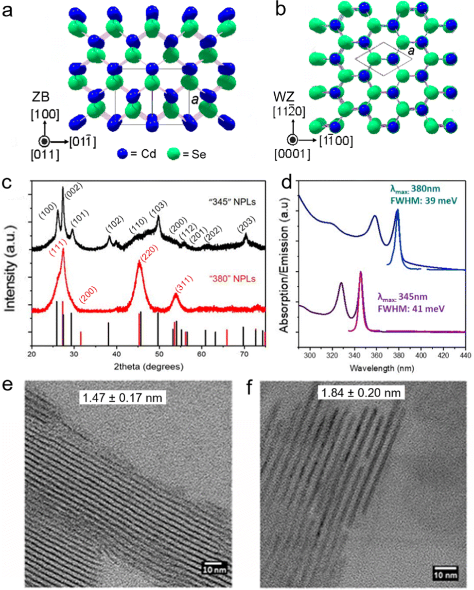 | ||
| Fig. 13 Schematic illustration of the crystal structure of (a) zinc blende and (b) wurtzite CdSe. Reproduced from ref. 175 with permission from American Chemical Society, copyright 2015. (c) XRD patterns of wurtzite (black) and zinc blende (red) ZnSe NPLs. (d) Absorption and PL spectra of wurtzite ZnSe NPLs with 1.47 nm thickness (purple) and zinc blende ZnSe NPLs with 1.84 nm thickness (blue). TEM images of (e) wurtzite ZnSe NPLs with 1.47 nm thickness and (f) zinc blende ZnSe NPLs with 1.84 nm thickness. Reproduced from ref. 37 with permission from American Chemical Society, copyright 2020. | ||
Generally, zinc blende CdSe NPLs are prepared in the presence of fatty acids, such as OA, myristic acid and carboxylates with short chains, at high temperatures (>200 °C). The obtained zinc blende NPLs possess tunable thickness, lateral size and composition, resulting in tunable optical properties.26,28,41 For wurtzite CdSe NPLs, they are prepared in the presence of fatty amines, including OAm, octylamine and so on, at elevated temperatures (≤200 °C).30,36–39 Most wurtzite NPLs possess a unique thickness of 4 MLs with a rectangular shape and their thickness can be tuned only in a small range.30,37,38 For example, ZnSe NPLs with the wurtzite phase were prepared in a mixture of OAm and octylamine using zinc stearate and Se powder. The obtained NPLs had a thickness of 4 MLs (∼1.47 nm), manifesting a sharp absorption peak at 345 nm (Fig. 13c–e). Further reaction between ZnSe NPLs with additional zinc stearate and Se powder led to an apparent red shift of the absorption peak from 345 nm to 380 nm and an increase of NPL thickness from 1.47 nm to 1.84 nm, (Fig. 13d and f), with an uncontrollable extension of lateral size being observed. This uncontrollable lateral dimension extension of NPLs was accompanied by a structure conversion from wurtzite to zinc blende (Fig. 13c). Unfortunately, no further details were provided to explain such a conversion.37 Additionally, Delikanli et al.42 prepared CdSe NPLs with 2 MLs by the reaction between Cd and Se precursors in a mixed solution containing fatty amine and a small amount of OA, but no crystalline phase data were provided.
For CdSe with a thickness less than 5 MLs, both wurtzite and zinc blende species exist simultaneously.176,177 In CdSe NPLs with the dominant zinc blende phase, as their thicknesses increased from 3 MLs to 4 MLs, the proportion of wurtzite species decreased from 17% to 11% and the wurtzite species disappeared when the thickness of NPLs increased to 5 MLs. Such a structural transformation from wurtzite to zinc blende in CdSe NPLs when their thickness increased can be attributed to the insertion of stacking faults at the alternate layers of wurtzite phase and the statistical insertion of deformation faults at a two-layer spacing.176 For CdS nanoplates obtained by the cation exchange reaction from covellite CuS nanoplates, a small fraction of wurtzite species was also observed.177 In this reaction, OAm was employed as the ligand, which can facilitate the transformation of a small fraction of CuS to digenite Cu7.2S4, resulting in a small fraction of wurtzite CdS species in the product obtained by the cation exchange from digenite Cu7.2S4 existing in CuS nanoplates. Besides zinc blende and wurtzite II–VI NPLs, the orthorhombic PbS nanosheets were also obtained. These orthorhombic PbS nanosheets possessed a direct bandgap transition, which was different from the orthorhombic SnS and GeS.67
The atomic layer deposition (ALD) technique is a powerful vapor phase technique to deposit alternating precursors on various substrates individually and sequentially to form ultrathin uniform thin films.179,180 Inspired by the ALD technique, Ithurria et al.46 developed a colloidal ALD (c-ALD) method to construct the core/shell structure for 2D NCs for the first time. The typical synthesis process is shown in Fig. 14a. The myristate-capped zinc blende CdSe NPLs were dispersed in toluene solution and mixed with formamide containing S2−. Since the basal planes of zinc blende CdSe NPLs were terminated with Cd2+,29 nucleophilic S2− could replace myristate on the surfaces of CdSe NPLs and bonded with electron-deficient Cd2+, leading to the formation of S2− capped CdSe (CdSe/S2−) NPLs and a phase transfer of CdSe NPLs from toluene to formamide (step I). The negatively charged S2− capped on the surfaces of NPLs provided enough electrostatic stability for the mono-dispersion of NPLs in the polar solvent, formamide. The upper toluene phase was replaced by the fresh toluene to remove residual organic ligands. Since di-n-dodecyldimethylammonium bromide (DDAB) possessed long hydrocarbon chains and positively charged DDA+ tightly bonded with negatively charged S2− on the surfaces of CdSe/S2− NPLs, CdSe/S2− NPLs were re-transferred into the upper toluene phase by adding DDAB (step II). After excess S2− in formamide was removed, the CdS shell layer could epitaxially grow by the reaction of fresh Cd2+ in formamide with S2− on the surfaces of CdSe/S2− NPLs (step III). By repeating this deposition process, a controlled shell layer thickness was achieved. Besides CdSe/CdS core/shell NPLs, HgTe/CdS core/shell NPLs with large lattice mismatch could also be prepared by using this strategy.181 Compared to the successive ionic layer adsorption and reaction (SILAR) method utilized for the preparation of core/shell QDs, this c-ALD method can achieve the layer-by-layer epitaxial growth of NPLs without any precise calculation of every half-reaction.46
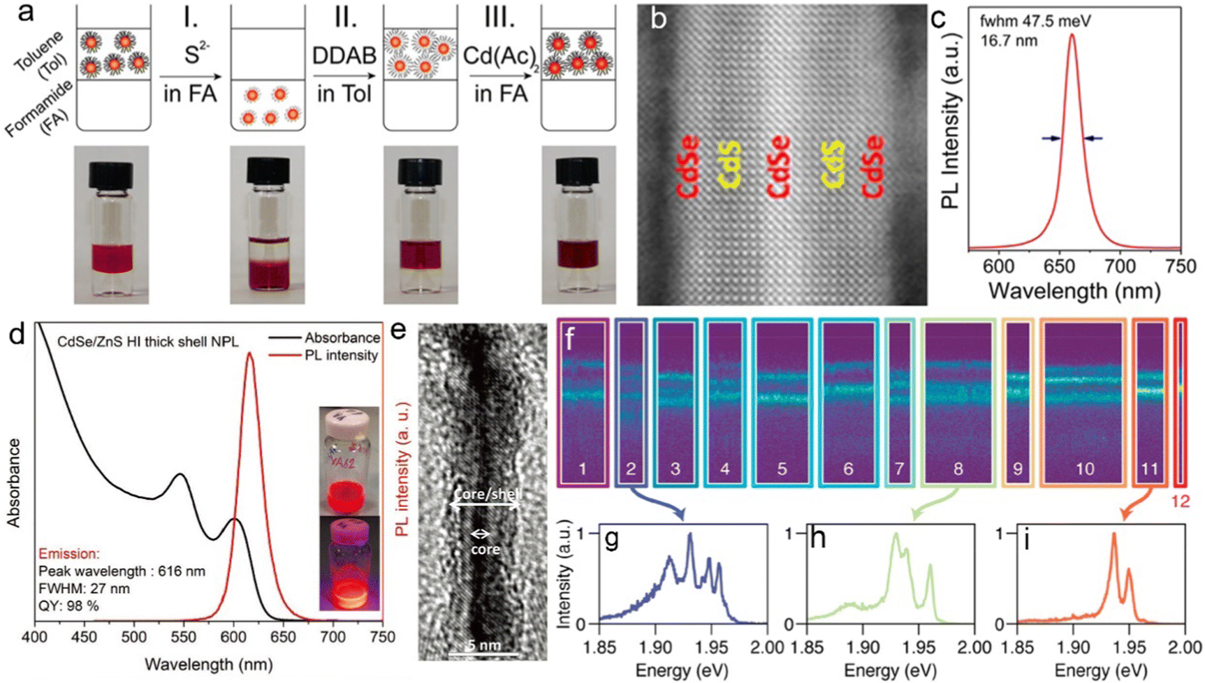 | ||
| Fig. 14 (a) Schematic illustration of the c-ALD method. Reproduced from ref. 46 with permission from American Chemical Society, copyright 2012. (b) HRTEM image of CdSe/CdS/CdSe core/shell/shell NPLs obtained by the c-ALD method. (c) PL spectrum of CdSe/CdS core/shell NPLs obtained by the c-ALD method. Reproduced from ref. 49 with permission from American Chemical Society, copyright 2019. (d) Absorption and PL spectra and (e) HRTEM image of CdSe/ZnS core/shell NPLs obtained by the hot-injection shell (HIS) method. Reproduced from ref. 80 with permission from Wiley-VCH copyright, copyright 2019. (f) Emission clusters of time-dependent emission spectra. (g-i) Average emission spectra for three clusters (2, 8 and 11) identified by machine learning. Reproduced from ref. 72 with permission from American Chemical Society, copyright 2019. | ||
Unfortunately, the use of the c-ALD method for the preparation of core/shell wurtzite semiconductor NPLs was unsuccessful, although it worked well for zinc blende semiconductor NPLs. To this end, Sun et al.182 developed a separate cation and anion deposition method to construct CdTe/CdSe and CdTe/CdS core/shell structures for wurtzite NPLs at room temperature. Cations were deposited on the surfaces of wurtzite CdTe NPLs by the surface ligand exchange from primary amine to Cd(OAc)2. Sequentially, CdSe or CdS shells were formed by the reaction between surface Cd(OAc)2 and selenourea or thiourea. By multi cycles of deposition processes, CdTe/CdS and CdTe/CdSe core/shell NPLs with total thicknesses of 3.0 nm and 6.3 nm, respectively, were achieved. However, the incomplete deposition (0.206 ± 0.007 monolayer) of the CdS shell in every deposition cycle and some stacking faults of zinc blende CdSe shell on wurtzite CdTe core surfaces still existed. Additionally, wurtzite Zn-based II–VI core/shell NPLs has not been achieved by this method, which might be caused by the low reaction activity of Zn(OAc)2 compared to Cd(OAc)2 at room temperature. Therefore, more efforts should be devoted to developing other strategies that can result in uniform epitaxial growth of the shell on the (110) planes of wurtzite NPLs.
Although the c-ALD method and separate cation and anion deposition method enable the heterostructures, the core/shell NPLs always have very low QY levels in the ranges of 1–4%,80 which may be caused by the low reaction temperature. In 2019, Hazarika et al.49 employed the c-ALD method at an elevated temperature of ∼150 °C to prepare CdSe/CdS core/shell NPLs. In this modified c-ALD method, the precursors were loaded on the ion-exchange columns or selected from salts poorly soluble in ODE and the NPLs served as mobile phases, which made it possible to grow the shell at ∼150 °C. The obtained core/shell CdSe/CdS NPLs have clear heterogeneous interfaces (Fig. 14b), a high quantum yield of 91% and an ultra-narrow PL FWHM of 16.7 nm (Fig. 14c), indicating that the interface defects and inhomogeneity of the core/shell structures prepared by this modified c-ALD method were significantly suppressed.
In order to simplify the shelling process, Mahler et al.76 developed a continuous shell growth method for core/shell NPLs. In a typical continuous shell growth process, thioacetamide and excess octylamine were mixed and added to NPL solution before cadmium precursor was introduced into NPL solution. Thioacetamide reacted with octylamine to release H2S and H2S was deposited on the surface of NPLs by reacting with surface Cd2+. Such S2− deposition was the key for the continuous shell growth. After S2− deposition, Cd precursor was added to the reaction solution to initiate shell growth at room temperature. However, during the shell growth process, the polytypic CdS shell layers appeared in CdSe/CdS core/shell NPLs. Adding Zn2+ (30%) to the Cd precursor could eliminate the polytypic structures, which might be caused by the difference of heterogeneous nucleation density or the Ostwald ripening process dependent on Zn2+ concentration.76 After the shell grew at room temperature, smooth and homogeneous core/shell NPLs were obtained by annealing at 300 °C for 30 minutes in the presence of trioctylamine and cadmium oleate. This continuous shell growth method enabled CdSe/CdZnS core/shell NPLs with a PLQY of 60% and red shifts of both first excitonic peak and emission peak.
Recently, the HIS growth performed at high temperature (300 °C) has enabled core/shell NPLs with high PLQYs (≥90%).78,80 However, ultra-thin core NPLs are easily etched at such high temperatures. Excess ligands and cation precursors of shells were demonstrated to stabilize ultra-thin core NPLs by providing better passivation for NPLs and largely preventing the dissolution of NPLs, respectively.75 In a typical HIS growth process, in the presence of Zn(OAc)2, OA and OAm, ZnS shells were deposited on the surfaces of CdSe NPLs by the reaction between Zn2+ and 1-octanethiol at 300 °C. The obtained CdSe/ZnS core/shell NPLs possessed a near-unity PLQY of 98% and well-defined interfaces (Fig. 14d and e). Furthermore, the ZnS shells substantially improved the stability of NPLs.80 In the thermal stability tests, CdSe/ZnS core/shell NPLs with thick shells exhibited 100% recovery of the initial PL intensity in the heating cycle from 300 to 400 K and 76% recovery in the heating cycle from 300 to 525 K.80
Despite the atomic flatness in core/shell NPLs, broadening of the emission line width can be still observed in such structures.71,75,76,80 Therefore, the broadening of emission line width may be derived from other origins. Tessier et al.71 demonstrated that the broadening of emission line width was caused by the strong exciton–phonon coupling in shells. For example, the FWHMs of the emission peaks of CdSe, CdS and CdTe NPLs with zinc blende structure were measured as 37 meV, 94 meV and 32 meV, respectively, indicating that CdS NPLs possessed larger exciton–phonon coupling strength compared to CdSe NPLs. For the CdSe/CdS core/shell NPLs, the FWHM emission peak was 60–70 meV, which was between those of CdSe and CdS NPLs. This meant that due to the delocalization of charge carriers in the shell, the excitons were coupled by phonon confined in both the core and the shell in core/shell NPLs.71
However, the emission line width of the ensembles of core/shell NPLs remains broad and becomes strongly asymmetric even at cryogenic temperatures, under which the phonon coupling should be suppressed. Therefore, other mechanisms accounted for the broadening of emission line width should be explored. Antolinez et al.72 demonstrated that the broadening of emission line width was derived from electron shakeup in core/shell NPLs. The time-resolved emission spectra of single CdSe/CdS NPL were measured at cryogenic temperatures. Surprisingly, the emission spectra of single NPL with an exposure time of one second contained a series of sharp peaks. The time traces of the PL intensity were analyzed by machine-learning algorithms. All spectral frames of 12 clusters in Fig. 14f exhibited similar emission spectra. By averaging all frames, high signal-to-noise ratio emission spectra were obtained, as shown in Fig. 14g–i. These spectra indicated that the NPLs switched between states with two to four dominant emission features. Such complex multiple emission peaks were consistent with electron “shakeup lines” from negatively charged trions, which was a form of the Auger coupling process.72 In this process, radiative recombination occurred within an electron–hole pair, while part energy was transferred to the remaining electron by exciting this electron to a higher single-electron level. The coupling between the trion ground state and the different shakeup lines was affected by the mobile surface defects or surface charges, which led to the broadening of the ensemble emission line widths.72 Additionally, the other mechanism may also account for such broadening of emission line width. The mirror charges could increase the confinement of the charge carriers. As the shell grew, the effect of mirror charges reduced and the position of mirror charges fluctuated in the whole core/shell NPL, resulting in the broadening of the emission line width.71
Except for the direct construction of the core/shell structure, CdSe based core/shell NPLs can also be utilized as a platform to produce core/shell NPLs with other compositions.183 For example, the 0D CdxHg1−xSe domains were embedded in the CdSe NPLs by the partial cation exchange reaction between CdSe NPLs and Hg(OAc)2. After epitaxial growth of CdZnS shells, the 0D CdxHg1−xSe domains embedded core/shell NPLs possessed a PLQY up to 55% and a bimodal PL band in the NIR region (700–1100 nm), which was caused by the bimodal distributions in size or composition of 0D CdxHg1−xSe domains on the long and short edges of rectangular NPLs.183
Tessier et al.73 achieved the lateral extension of CdS on all sidewalls of CdSe NPL cores with different core sizes. In typical CdSe/CdS core/crown NPLs with 5 MLs, as the CdS crown size increased, the absorption intensity in the high energy region increased and the high PLQY of such NPLs reached 60%, as shown in Fig. 15a. The CdSe/CdS core (small)/crown NPLs exhibited broader (13–14 nm) emission FWHM compared to core-only or core (large)/shell NPLs (8 nm) with the same thickness as well as compared to single CdSe/CdS core (small)/crown NPL (11.5 nm), which indicated that some dispersity of core (small)/crown NPLs contributed to slight broadening of the emission line width of ensemble NPLs and these NPLs possessed an intrinsic larger emission line width compared to core (large)/crown NPLs.73 The PL lifetimes of CdSe/CdS core/crown NPLs with different lateral sizes evolved with temperatures. As the temperature decreased, the PL lifetime of core (large)/crown NPLs shortened accompanied by an increase of the PL intensity and an average lifetime of 200–300 ps was achieved at 10 K (Fig. 15b top). Core (small)/crown NPLs behaved differently from the core (large)/crown NPLs. As the temperature decreased, the PL lifetime of core (small)/crown NPLs increased and the PL intensity decreased slightly. When the temperature was 10 K, the PL decay of core (small)/crown NPLs was fitted by a biexponential curve consisting of a shot lifetime component of 1.4 ns (10% of the emitted photons) and a long lifetime component of 380 ns (90% of the emitted photons) (Fig. 15b bottom). In the exciton fine structure, two emissive states including an authorized state |A〉 with a large oscillator strength and short lifetime and a forbidden state |F〉 with a small oscillator strength and long lifetime accounted for the biexponential lifetime. The energy gaps between |F〉 and |A〉 in core (large)/crown and core (small)/crown NPLs were 5 meV and 2 meV, respectively. For core (small)/crown NPLs, as the temperature decreased, the exciton was trapped in the forbidden state |F〉, resulting in a long PL lifetime. While for core (large)/crown NPLs, the forbidden state |F〉 was not observed in core (large)/crown NPLs at 10 K because there was a thermal equilibrium between |F〉 and |A〉.73
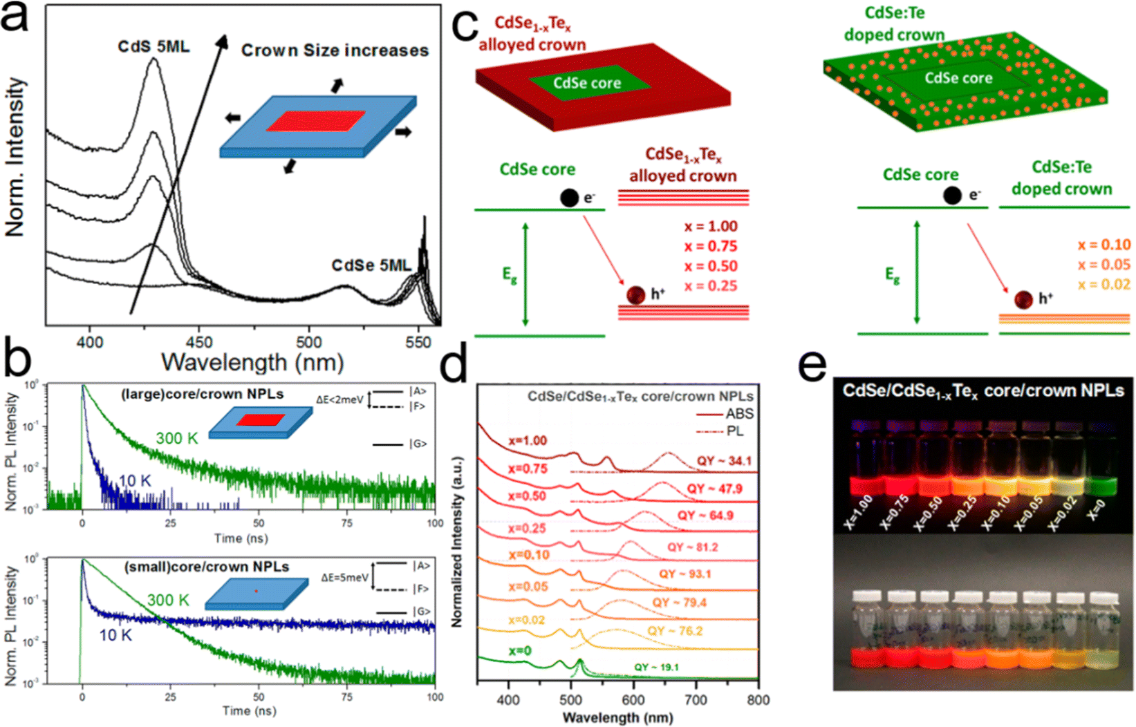 | ||
| Fig. 15 (a) Absorption spectra of core/crown CdSe/CdS NPLs with different crown sizes. (b) PL decay curves of CdSe/CdS core/crown NPLs with different core sizes at room and cryogenic temperatures. Reproduced from ref. 73 with permission from American Chemical Society, copyright 2014. (c) Schematic illustration of band diagrams of CdSe/CdSe1−xTex core/crown NPLs for x ≥ 0.25 (left) and x ≤ 0.25 (right). (d) Evolution of the absorption and PL spectra of CdSe/CdSe1−xTex core/crown NPLs. (e) Digital photos of CdSe/CdSe1−xTex core/crown NPLs under UV illumination (top) and ambient light (bottom). Reproduced from ref. 187 with permission from American Chemical Society, copyright 2017. | ||
In order to further improve the PLQY of type-I core/crown NPLs, Hu et al.185 constructed alloyed CdSeS crowns on the sidewalls of 4 ML CdSe NPLs, leading to green-emitting CdSe/CdSeS core/crown NPLs with a near-unity PLQY and a narrow emission FWHM of 15 nm. In the typical synthetic process, S precursor was added at different times during the lateral extension of CdSe NPLs to facilitate the growth of CdSeS crowns by combining with unreacted Se precursor, resulting in the suppression of interface defects. However, incorporating the alloyed CdSeS crowns only was not sufficient for the 3.5 ML CdSe/CdSeS core/crown NPLs to achieve the near-unity PLQY. This was because the interface defects were not completely suppressed by the asymmetrical growth of CdSeS crowns on the sidewalls of rectangle-shaped 3.5 ML CdSe NPLs due to the unfavorable growth of (110) facets induced by the adsorption of short-chain ligands.186 As Cd(propionate)2 was employed instead of propionic acid, the high ratio of Cd and Se precursors altered the growth directions from [100] to [110]. Therefore, triangular 3.5 ML CdSe NPLs with a symmetrical shape were obtained, facilitating the symmetrical growth of CdSeS crowns.186 The obtained blue-emitting triangle-shaped 3.5 ML CdSe/CdSeS core/crown NPLs possessed a narrow emission with a FWHM of 10 nm and a near-unity PLQY. The combination of alloyed and asymmetrical crowns provided a possibility for NPLs with near-unity PLQY but without any broadening of emission, which enabled the high color purity blue and green LEDs.185,186
The epitaxial growth of CdSe crowns on the sidewalls of CdS NPLs results in inverted type-I CdS/CdSe core/crown NPLs, and both CdS cores and CdSe crowns possess same thickness.188 In CdSe/CdS core/crown NPLs, due to the strong exciton confinement in the CdSe NPL core, the emission energy is independent of the lateral size of CdS crowns. However, because the excitons are predominantly located in CdSe crowns, changing the lateral size of the CdSe crown can alter the PL properties. At the beginning of CdSe crown growth, the band edge and trap emissions of CdS NPL cores are dominant. As the growth of CdSe crown evolves, both band edge and trap emissions of CdS NPL cores are eliminated gradually due to the fast transfer of charges from CdS cores to CdSe crowns. Simultaneously, the emission peak shifts from 460 nm to 515 nm, which corresponds to the core-only CdSe NPLs with 4ML thickness, and a PLQY of 55% is obtained. The band edge emission line width is broad at the initial stage of CdSe crown growth, which is attributed to the lateral size distribution of CdSe crowns. As the CdSe crowns grow large, the band edge emission line width becomes narrow because the CdSe crowns are confined only along the vertical direction. By a combination of narrow band edge emission (blue-green) and broad trap emission (yellow-red), these inverted type-I CdS/CdSe core/crown NPLs enable white light-emitting devices with a CRI of 80.188
Type-II core/crown NPLs, including CdSe/CdTe and CdSe/ZnSe, are another commonly observed structure of core/crown NPLs.189,190 These type-II core/crown NPLs always possess a broad and large Stokes shift emission recombined at the interfaces.47,187,190 The type-II CdSe/CdTe core/crown NPLs were prepared in 2014 for the first time.47 Due to the band offsets of 0.42 eV and 0.57 eV in the conduction bands and valence bands, respectively, the electron wave function was located in CdSe cores while the hole wave function was located in the CdTe crowns. Such spatial separation enabled the charge recombination across the heterointerfaces, exhibiting a large Strokes shift emission at 730 nm, which was larger compared to the red shift observed in the type-I CdSe/CdS core/crown NPLs. Additionally, the emission peak position could be mediated by depositing CdTe crowns on CdSe NPL cores with different thicknesses.47 Additionally, as the deposition of CdTe crown proceeded, the emission line width became broad. Considering the precise control of the thickness, such broadening should be attributed to the increased phonon coupling due to the spatial separation of electrons and holes.47 These type-II CdSe/CdTe core/crown NPLs possessed a PLQY of 50%, which could be improved to 70% by incorporating a gradient interface.47 Such gradient interface was obtained by introducing Cd and Te precursors during the formation of CdSe NPLs. Another group demonstrated that by the construction of CdSe1−xTex alloyed crowns on the sidewalls of CdSe NPL cores, the emission peak position was mediated from 570 nm to 660 nm without any changes of thickness (Fig. 15c–e).187 Two obvious broad emission peaks could be observed as x ≥ 0.25 and x ≤ 0.10. In the former case, the increase of Te concentration contributed to the formation of CdSe1−xTex alloyed crowns, resulting in a type-II structure (Fig. 15c, left). A broad emission originated from the recombination of the electrons in the conduction band in CdSe cores and the holes in the valence band in alloyed crowns, and its broad line width was the common feature in other type-II NCs. In the latter case, the low Te concentration contributed to the formation of the doping structure in CdSe crowns, as shown in the right panel of Fig. 15c. A broad emission emerged by the recombination of electrons in the conductor band in CdSe cores and the holes in the doping energy level in crowns. Eventually, a high PLQY of ∼95% was obtained in these type-II core/crown NPLs as x = 0.10. The following three factors are expected to be responsible for such a high PLQY. First, the alloy crowns contribute to the overlap of electron and hole wave functions. Second, the substitution of Te atoms by Se atoms in crowns decreases the lattice mismatch between cores and crowns, reducing the trap sites caused by lattice strain or defect. Finally, the ultra-fast charge separation at the interfaces of cores and crowns results in the suppression of nonradiative recombination due to the large in-plane exciton mobility.187
The CdSe/CdSe1−xTex core/crown NPLs can also facilitate bicolor emission by changing the Te concentration in crowns.191 It is noted that in type-II CdSe/CdTe core/crown NPLs, only the emission at the interfaces can be observed because the holes are always located in CdTe crowns. Therefore, it is difficult to observe band edge emission of CdSe cores. The high concentration of Te can result in larger conductor band offsets compared to the exciton binding energy. Therefore, the electrons reach the cores and are radiatively recombined at the interfaces. Dufour et al.191 demonstrated that the CdSe0.4Te0.6 crown could enable the bicolor emission. In such a CdSe0.4Te0.6 crown, the conductor band offset was less than the exciton binding energy. The electrons felt both the conduction band offset and the strong attractive Coulomb interaction with holes, resulting in two emissions, in which one emission was derived from the radiative recombination at the core/crown interfaces and the other emission originated from direct recombination in the crowns, which was not detected previously in CdSe/CdTe core/crown NPLs due to the large binding energy.191
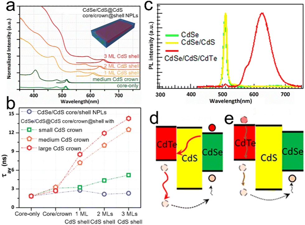 | ||
| Fig. 16 (a) Absorption/PL spectra and (b) amplitude-averaged PL lifetime of the core, core/crown, core/shell, and core/crown@shell NPLs. Reproduced from ref. 48 with permission from American Chemical Society, copyright 2016. (c) PL spectra of CdSe, CdSe/CdS core/crown and CdSe/CdS/CdTe core/barrier/crown NPLs. Band alignment and photoexcitation schemes of (d) two-photon and (e) three-photon upconversion excited at 640 nm and 1064 nm, respectively. Reproduced from ref. 82 with permission from American Chemical Society, copyright 2020. | ||
4.2 Surface engineering
0) planes and possess the same amount of cations and anions. Therefore, only neutral ligands, and L- and Z-type ligands, can be ligated on the surfaces. (110) planes are composed of alternating and parallel ridges and valleys. Cd2+ and Se2− of wurtzite CdSe NPLs located at the ridge positions of (110) planes are three-fold coordinated and available for ligands, while Cd2+ and Se2− located at the valley positions are sterically saturated and unavailable for ligands.118 The L-type ligands are capped to Cd2+ located at the ridge positions and the Z-type ligands are capped to Se2− located at the ridge positions.118 On the surfaces of wurtzite CdSe NPLs, reversible ligand exchange can be achieved by changing the concentration difference between L- and Z-type ligands, while X-type ligands may result in the instability of wurtzite CdSe NPLs.194 For the zinc blende CdSe NPLs, the top and bottom surfaces are (100) planes and terminated by Cd2+, which is regarded as an extra half monolayer. In order to balance charge, the X-type ligands, typically carboxylates, containing an extra electron are capped on the surface Cd2+ and can be exchanged by other X-type ligands, such as halides. Sun et al.117 demonstrated that the Z-type ligand could be exchanged by an L-type ligand after a slow ligand exchange process, indicating that the surface reconstruction occurs.117
| Surface ligand types | Molecular formulas |
|---|---|
| X-Type | RCOO−, Cl−, R-S−, etc. |
| L-Type | PR3, RHN2, etc. |
| Z-Type | Cd(RCOO)2, CdCl2, Pb(SCN)2, etc. |
Except for ligand exchange strategy, coating macromolecule ligands on the surfaces of NPLs can produce water-soluble NPLs as well.200,201 For example, Lim et al.201 demonstrated that the nanodisc composed of phospholipids and lipoproteins could achieve water-soluble CdSe/CdS core/shell NPLs. In these water-soluble CdSe/CdS core/shell NPLs, phospholipids were bounded to the top and bottom planes of NPLs, while lipoproteins were bounded to the sidewalls of NPLs, contributing to long-term stability in biological buffers and high-salt solutions. Despite an obvious decrease of PL intensity, these water-soluble CdSe/CdS core/shell NPLs enabled a rapid internalization into living cells. In order to maintain the PLQY after phase transfer from the nonpolar phase to the polar phase, Halim et al.200 utilized dodecyl-grafted-poly(isobutylene-alt-maleic acid) to achieve water-soluble CdSe/CdZnS core/shell NPLs. In a typical phase transfer process, CdSe/CdZnS core/shell NPLs were mixed in a solution of dodecyl-grafted-poly(isobutylene-alt-maleic acid), in which 75% anhydride rings were opened by dodecylamine and the rest served as anhydride groups. The hydrophobic side chains of dodecyl-grafted poly(isobutylene-alt-maleic acid) interacted with the hydrophobic ligands of NCs via hydrophobic forces and the anhydride rings provided negatively charged carboxylate groups on the surface of NPLs after water transfer. The mixture containing NPLs and dodecyl-grafted poly(isobutylene-alt-maleic acid) was dried using a rotatory evaporator and boric acid buffer (pH = 12) was employed to open all the anhydride rings (Fig. 17a). Benefiting from the protection of CdZnS and polymer shells, the PL intensity of water-soluble NPLs similar to that of intrinsic NPLs was preserved and would not be quenched in phagolysosomes despite the harsh conditions (pH = 4.5–6.5) (Fig. 17b), demonstrating the enormous potential of such water-soluble core/shell NPLs for bioimaging applications.
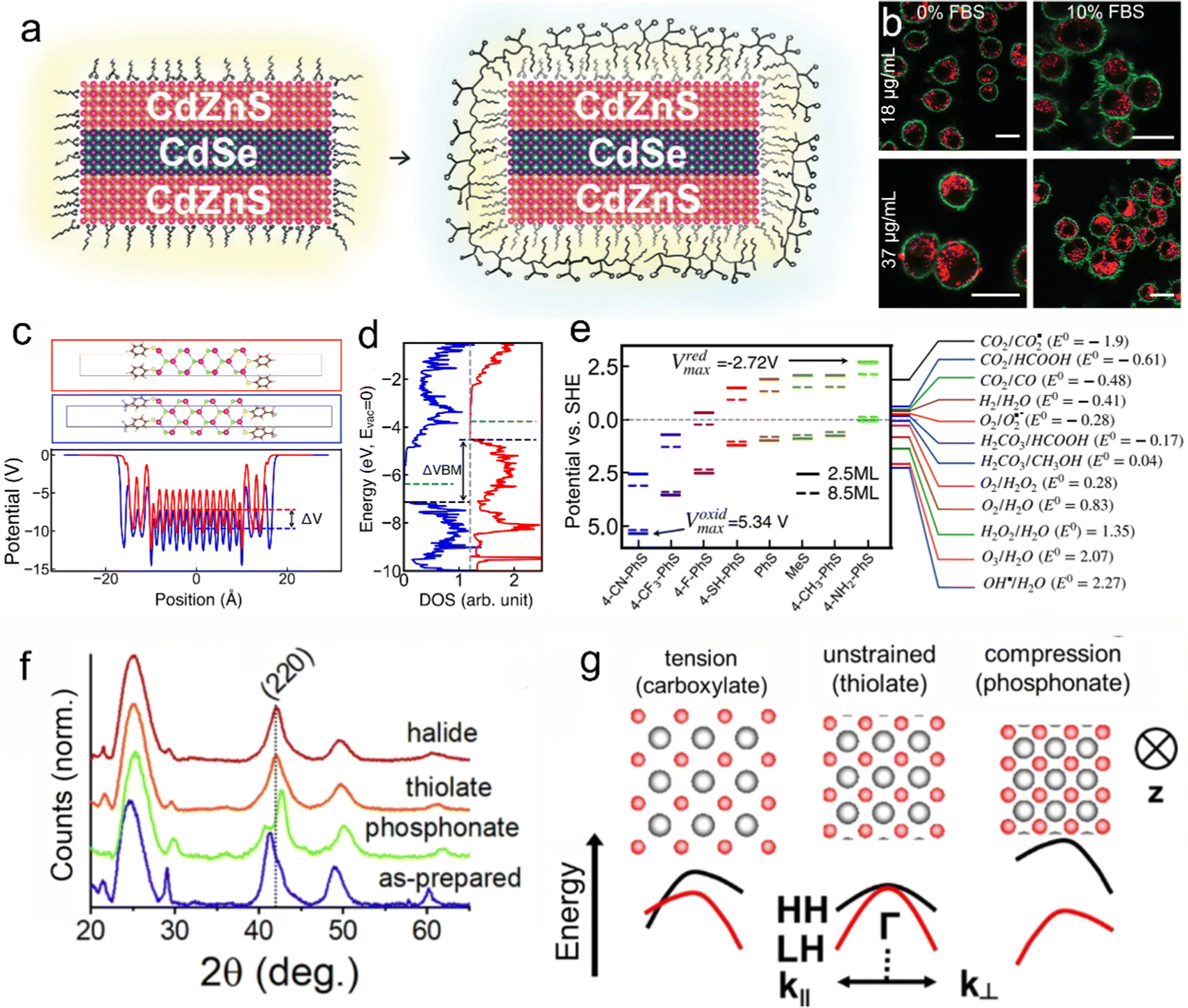 | ||
| Fig. 17 (a) Schematic illustration of polymer coating of semiconductor NPLs. Hydrophobic regions are high-lighted in yellow and hydrophilic regions are high-lighted in blue. (b) Intracellular localization of the NPLs was confirmed by confocal laser scanning microscopy. Reproduced from ref. 200 with permission from Royal Society of Chemistry copyright 2020. (c) Two-dimensional approximant (top) and planar-averaged electrostatic potential (bottom) along the quantum-confined out-of-plane direction of C6H5-S- (red) and 4-CF3-C6H4-S- (blue) capped 6.5 ML CdSe NPLs, (d) DOS of C6H5-S- (red) and 4-CF3-C6H4-S- (blue) capped 6.5 ML CdSe NPLs. (e) Band edges of CdSe NPLs with different ligands and the reduction potentials for reactions. Reproduced from ref. 202 with permission from American Chemical Society, copyright 2019. (f) XRD patterns of the as-prepared, phosphonate capped, thiolate capped and halide capped CdSe NPLs. (g) Anticipated band distortions under biaxial strain. Reproduced from ref. 203 with permission from American Chemical Society, copyright 2019. | ||
Ligands were demonstrated to change the band gaps of NPLs as well and the reasons responsible for these changes of the band gaps were proposed. The narrowing of band gap was once considered as the consequence of weakening quantum confinement caused by the increase of NPL thickness after ligand exchange.46,76 Additionally, delocalization of wavefunction caused by the strong mercury–thiol interaction was regarded as another origin for an obvious absorption peak red shift of ∼250 nm in HgTe NPLs.205 Recently, the strains induced by ligand exchange have been demonstrated to cause the variation of band gap as well. Compressive strains can decrease bond distances in NCs and thus contribute to an increase of both orbital overlap and effective band gaps, whereas tensile strains can increase bond distances in NCs and thus contribute to a decrease of both orbital overlap and effective band gaps.206 For wurtzite CdSe NPLs, the intrinsic amine ligands result in a contraction of 3.4% in the a axis. After ligand exchange by metal carboxylates, the contraction in the a axis decreases obviously (0.9% for Cd(oleate)2 and 1.9% for Zn(oleate)2). Therefore, when the intrinsic amine ligands are exchanged by Cd(oleate)2, both tensile strain and confinement dimensionality result in a decrease of the band gap (∼140 meV). When the intrinsic amine ligands are exchanged by Zn(oleate)2, only tensile strain results in a decrease of band gap (∼50 meV). The larger absorption peak red shift of Cd(oleate)2 capped CdSe NPLs compared to that of Zn(oleate)2 capped CdSe NPLs is caused by the effective thickness increase by Cd in Cd(oleate)2. A decrease of band gap (∼240 meV) induced by ligands was also observed in zinc blende CdSe NPLs.207 Surface ligands have also led to a considerable distortion of zinc blende unit cells. When the intrinsic carboxylate ligands were exchanged by 1-hexadecanethiol or n-hexadecylphosphonic acid, the lateral contraction of the lattice resulted in a perpendicular expansion of NPL thickness, thus resulting in an obvious red shift of the absorption peak. Several factors were believed to contribute to the lattice transformation, such as the mismatch of bonds in cores and interfaces, coverage of ligands on the surface and the formation of hydrogen bonds.207 Besides the strains in one axis, the strains in bi-axis partially contributed to the red shift of absorption peak in NPLs.203 The diffraction peaks of the (220) planes revealed that obvious strains existed in 5.5 ML CdSe NPLs (Fig. 17f) and consisted of a narrow peak and a broad peak, which were assigned to the strains both in the short axis and the long axis, respectively. Compared to the as-prepared (carboxylate capped) and thiolate capped NPLs, phosphonate capped CdSe NPLs possessed the largest variation of energy from heavy hole to light hole (Fig. 17g), indicating that a large in-plane compressive strain existed in phosphonate capped NPLs. This compressive strain was large enough that the increased energy of valence band edge contributed more than delocalization alone, resulting in the red shift of band gap.203
5. Optoelectronic properties
5.1 Narrow emission line width
Semiconductor NPLs exhibit three distinctive features compared with QDs of the same component when their emission peaks are the same: narrower emission line width, tinier Stokes shift and shorter PL lifetime.208 The PL emission line width of ensemble emitters can be affected by both inhomogeneous and homogeneous broadening. Inhomogeneous broadening is induced by a variation in emission wavelength between different emitters (e.g., variation in NPL thickness) and not particularly temperature-dependent. Homogeneous broadening of exciton emission in NPLs depends on lifetime broadening.209 The Heisenberg uncertainty principle states that the shorter the coherence lifetimes of the excited states, the larger the uncertainty in excited state energy levels, and thus the broader the emission line width. The main reason for the rapid decrease of the coherence lifetime upon heating is the interaction with phonons. The phonon-induced exciton dephasing process is strongly temperature-dependent, leading to the broadening of the homogeneous line of exciton emission. As the number of phonons increases, the exciton emission becomes uniformly broadened with temperature.210 At room temperature, the ensemble emission spectrum of NPLs is almost the same as that of the single-particle one and PL without inhomogeneous broadening since the NPLs have the property of adjustable thickness at the atomic scale, while the ensemble emission spectrum of QDs is different from that of single particle due to the size differences. The emission FWHMs of NPLs at room temperature typically range from 7 to 10 nm, corresponding to the line width between 1kbT and 2kbT.211 Compared to 0D QDs and 1D NRs, the narrower PL spectra of NPLs show homogeneous broadening along the diagonal and non-homogeneous broadening perpendicular to the diagonal.112The phonon interaction affects the emission peak position of PL, whose shift depends on the phonon coupling and the thermal-dependent lattice expansion.209,213 Phonon-induced spectral shift is minimized due to the freezing of phonon vibrations at low temperatures (such as 4 K), and therefore inhomogeneous broadening of the ensemble spectrum can be observed. The NPLs of different thicknesses (3.5 ML, 4.5 ML) exhibit a similar inhomogeneous broadening (∼18 meV), which reflects that the thickness of the NPLs is indeed determined and is the same in the ensemble NPLs. Inhomogeneous broadening of QDs is larger than that of NPLs, varying between 70 meV and 90 meV (Fig. 18a and b); however, the inhomogeneous broadening becomes smaller when the size of the particles increases, due to the ease of achieving a small-size distribution for larger particles and the smaller effect of size variation on the emission energy (weaker confinement effect). As the temperature increases, the coupling of exciton–phonons process reduces the coherence lifetime of the excited states, which leads to homogeneous broadening of the emission line width. The emission line width depends on the dephasing processes in the lower energy phonon modes at low temperatures, and the activation of higher optical modes at higher temperatures leads to additional dephasing processes, including higher-order two-phonon processes.209
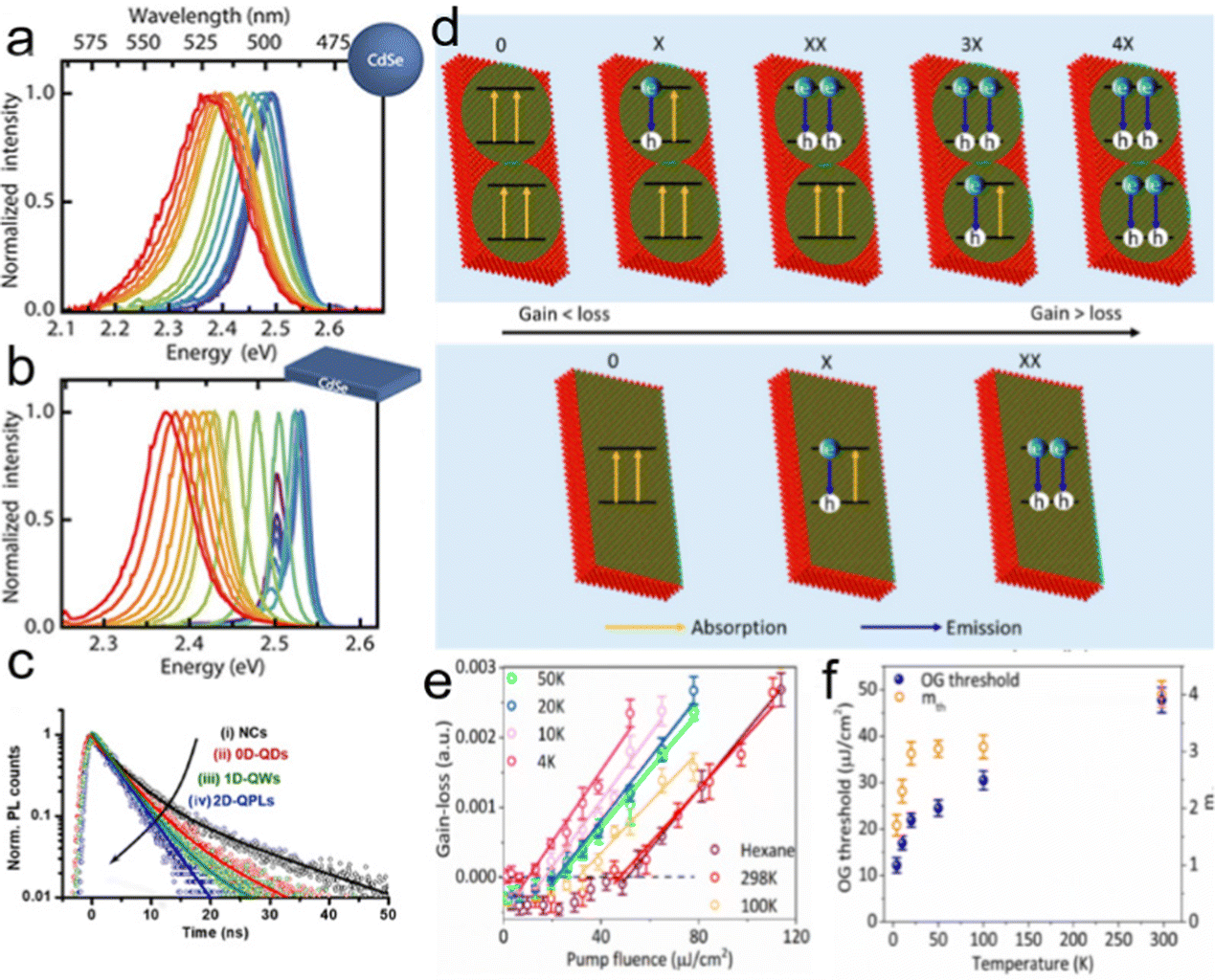 | ||
| Fig. 18 Normalized temperature-dependent PL spectra of (a) QDs and (b) NPLs. Reproduced from ref. 209 with permission from American Chemical Society, copyright 2020. (c) Time-resolved PL spectra of NCs, QDs, colloidal quantum wells (CQWs) and NPLs. Reproduced from ref. 212 with permission from American Chemical Society, copyright 2021. (d) Temperature-dependent OG mechanism, including a scheme of different exciton states in NPLs at room temperature with a saturation number of band-edge excitons (NS) of 4 and a scheme of different exciton states in NPLs at low temperatures (<4 K), the exciton center-of-mass coherence was delocalized throughout the whole NPL due to the GOST effect, giving NS = 2. (e) Normalized OG amplitude (at ∼2.34 eV, 2–3 ps) at different temperatures as a function of pump fluence, where the intercept on the x axis (black dashed line) gives the OG threshold. (f) OG threshold and average exciton number per NPL at the OG threshold (mth) of NPL in hexane as a function of temperature. Reproduced from ref. 88 with permission from American Chemical Society, copyright 2020. | ||
The trion emission, a quasiparticle consisting of an exciton and an additional charge carrier, dominates the exciton emission below 100 K in CdSe NPLs.173,214 However, such an emission is negligible in core-only QDs at all temperatures because the Auger recombination outcompetes radiative pathways. Since NPLs with large lateral dimensions exhibit slow Auger recombination rates and enhanced radiative rates, the trion emission outcompetes Auger recombination at temperatures as high as 200 K.215,216 Trions are the dominant emissive species in CdSe NPLs when the temperature is below 100 K, and the FWHM of trion emission (0.64 meV at 5 K) is similar to an exciton line width (∼0.4 meV at 5 K).217 The interpretation of the band-edge emission in CdSe NPLs is controversial. Their PL spectrum at cryogenic temperatures typically consists of distinct two-color emissions. High-energy lines are generated by neutral exciton complexes,218,219 while the origin of the low-energy lines is still debated. Longitudinal optic phonon-assisted exciton recombination, trion emission, emission from excimer states in neighboring NPLs, and recombination of exciton states from ground s-types are the potential options.166,172,220 Vong et al.221 demonstrated that the biexciton-to-exciton hole capture seems to be the main formation mechanism of triplet ions in undoped NPLs, even in the case of chemical electron doping, without direct absorption into the triplet ion state. Shornikova et al.222 revealed that the low-energy line originates from the recombination of negatively charged excitons (trions). As the temperature decreases, both the high-energy-peak and low-energy-peak shift to higher energies, and the intensity of low-energy emission increases with respect to that of high-energy emission.221 The blue-shift of the luminescence is caused by the temperature-dependent CdSe lattice structure and the electron-lattice coupling, which is called the “Vashni effect”.223 Moreover, the absence of low-energy absorption indicates that the negative trions in CdSe NPLs are not directly formed in the ground state by photoexcitation, even though there are excess electrons available through doping.221
5.2 Short PL lifetime
Compared to their QD counterparts, the NPLs present much shorter PL lifetimes (Fig. 18c),212 and the fast PL decays are associated with their GOST. Morgan et al.224 calculated the radiative rate value for 4.5 ML CdSe NPLs through the Einstein relations.225 The extinction coefficient at the heavy hole maximum is 1.75 × 10⁷ and the corresponding line width is ∼8 nm. The calculated radiative lifetime is 53 ps, which is in agreement with that measured at low temperatures. The electron and hole are delocalized over almost the entire NPL, and the overlap integral of electron and hole wave function is close to unity at low temperatures.226 However, the electron and hole can interact with the acoustic phonons, the overlap of electron and hole decreases, and the coherent volume of excitons in the NPL decreases with increasing temperature, as a result, a loss of GOST occurs, and the radiation lifetime increases to a few nanoseconds (4–6 ns), which is about an order of magnitude smaller than that of QDs at RT.23,227The advantages of NPLs, such as narrow emission line width and high gain coefficients, make them favorable in LEDs and lasers, while the applications of NPLs that rely on short PL lifetimes are rare. Recently, efficient scintillators based on perovskite NCs have been widely reported as a result of their high stopping power.228,229 However, the development of ultrafast scintillators for particle physics detection has been stalled due to the lack of high-quality sub-nanosecond-lived perovskite QDs. The PL lifetime of perovskite can be tuned by controlling the thickness and composition of the material, thus facilitating the development of ultra-fast scintillation devices.
5.3 High gain coefficient
The large absorption cross-section,230 low multiple exciton AR rates,215,231 and narrow emission line width208 of NPLs are beneficial for obtaining low OG threshold of these materials. The absorption cross-section per unit volume is much larger in NPLs compared to QDs,230 and increasing lateral dimension of NPLs could enhance biexciton Auger lifetimes, suggesting that enlarged lateral size of NPLs could reduce the OG threshold.215 However, the spatially separated excitons could appear in laterally enlarged NPLs, leading to an increase in the maximum number of band-edge exciton states (NS) (NS > 2). OG can be achieved when the band-edge exciton states are occupied by more than half; therefore, the OG threshold (mth) corresponds to >1 (QDs) and >NS/2 (NPLs) for the average number of excitons per emitter (Fig. 18d). The OG in NPLs can be realized when the number of excitons is greater than 1, which is produced by the absorption of multiple photons (>2). The short lifetimes of biexciton/multiexciton states are not beneficial to OG thresholds; however, the radiative processes do have to outcompete non-radiative ones.The OG mth is related to the average exciton number per NPL, which can be calculated using the follow equation:
 | (10) |
Since the thickness of the NPLs can be precisely controlled at the atomic layer level, NPLs have the same confinement energy in the lateral dimension. In the case of neglecting phonon and surface defect scattering, the intensity of the band-edge transition oscillator is concentrated to a single transition state with the lowest energy in K-space, resulting in the GOST effect, and accordingly, the exciton center-of-mass delocalization domain in real space can be coherently extended to the entire NPL. At low temperatures, the spatial region of center-of-mass coherence can be extended throughout the NPLs, which leads to a double degenerate band-edge exciton state (Fig. 18d, bottom), and tremendously enhances the radiative decay rate of the exciton (GOST effect). Based on the temperature-dependent OG threshold and exciton center-of-mass coherent delocalization in colloidal CdSe NPLs, ∼4-fold lower OG threshold at 4 K compared to that at room temperature (298 K) was achieved (Fig. 18e and f).88 The lower OG threshold at low temperatures is due to the expansion of the exciton coherence area, which reduces the saturation number of the band-edge excitons, enabling biexciton gain and increasing the radiation attenuation rate, consistent with the giant oscillator intensity conversion effect.88
5.4 Polarized luminescence
Polarized light is a phenomenon in which semiconductor materials produce anisotropic PL along different axes under the excitation of nonpolarized light. The polarized PL is usually dominated by the anisotropic crystal structure or semiconductor morphology. The polarization ratio is a parameter that allows measuring the degree of polarization and can be defined as235–238 | (11) |
 | ||
| Fig. 19 (a) Hypercrystalline structure schematic diagram of self-assembly of CdSe NPLs. (b) Epifluorescence measurements as a function of microneedles along the polarization direction and individual microneedles of false-color fluorescence intensity depending on the polarization direction. Reproduced from ref. 232 with permission from American Chemical Society, copyright 2013. (c) Scheme of kinetically driven face-down assembly and edge-up assembly. Reproduced from ref. 233 with permission from American Chemical Society, copyright 2020. (d) Simulated back focal plane imaging for dipole emission of CdSe NPLs. Reproduced from ref. 234 with permission from American Chemical Society, copyright 2017. | ||
Interestingly, unlike other nanostructures, NPLs can self-assemble in two ways: face-down assemblies and edge-up assemblies.233,234 Momper et al.233 control the CdSe NPLs orientation with entirely face-down or edge-up configurations through the solvent evaporation rate which can be kinetically adjusted by solvent, temperature or solvent partial pressure (Fig. 19c), and the resulted monolayer films with controlled CdSe NPLs exhibit long-range order of transition dipole moments and macroscopically polarized light emission. Gao et al.234 presented a liquid–liquid interfacial assembly method for the assembly of CdSe NPL films and provided an experimental determination of the exciton transition dipole orientation (Fig. 19d). Once the aligned transition dipoles are generated, the polarization properties of the semiconductor aggregation materials is amplified to maximize linearly polarized PL. These observations suggest that NPLs can be self-assembled to achieve adjustable and strong polarization properties and thus become a good candidate material for polarized light-emitting applications.
5.5 Fast multiexciton transfer
FRET is a nonradiative energy transfer induced by electromagnetic dipole–dipole coupling when PL and absorption spectra of two different luminaries overlap and has been extensively explored in various nanostructure.240–242 Although the FRET often decreases the PLQY of luminescent materials, researchers have found that it can promote the increase of charge carriers in photovoltaics by suppressing the AR.58 AR is a three-particle effect in which an electron and a hole generate recombination and transfer energy to another electron or hole. The large AR rate in the nanostructures leads to the rapid decay of the multi-exciton population, which will greatly increase the threshold of OG. Due to the strict momentum conservation constraints of NPLs, the monolayer-thick NPLs with lateral dimensions of tens of nanometers exhibit strong optical transitions and the decay time of AR can be hundreds of picoseconds which is much longer than that of 0D nanostructures.58,243 The small interplate distance coupled with large PL and absorption spectra overlapping can enhance the interaction and minimize spatial separation between NPLs, leading to an efficient and fast FRET process.58,243 Rowland et al.58 examined CdSe NPLs and showed a FRET of ∼6–23 ps, 15–50 times faster than AR. Coolen et al.57 measured a (1.5 ps)−1 FRET rate by imaging self-assembled linear chains of CdSe NPLs over 90 platelets, which is the fastest decay time reported in the literature. The fast FRET rate can accumulate multiple electron–hole pairs in the acceptor NPLs or separate multiple excitons contained in the donor NPLs before exciton annihilation by AR, and thus the threshold for optical amplification can be lowered and may contribute to carrier multiplication.244 Additionally, the charge transfer of NPLs with different electron- and hole-acceptor molecules has been investigated in NPL-based hybrid materials for photocatalysis or photovoltaic applications.176,245–248 Taghipour et al.246 studied a FRET process as a function of the distance between the CdSe/CdS NPL donor and MoS2 monolayer acceptor and a near-unity energy transfer efficiency of 99.88% with an ultrafast FRET lifetime of 3.73 ps from the ensemble thin films of CdSe/CdS NPLs to a MoS2 monolayer were obtained. Dutta et al.249 investigated the charge transfer dynamics of 2D CdSe NPLs in the presence of benzoquinone molecule using steady-state and transient absorption spectroscopy and confirmed the ultrafast electron transfer from CdSe NPLs to the benzoquinone molecule. The photodetector based on hybrid materials demonstrated better prominent photoelectric characteristics than pure NPLs. These properties of fast multiexciton transfer in NPLs make such nanostructured materials ideal candidates for low-threshold optical techniques.5.6 Circular dichroism
Circularly polarized light can be divided into left-handed circularly polarized (LCP) light and right-handed circularly polarized (RCP) light. Circular dichroism (CD) refers to the differential absorption of LCP and RCP. The degree of CD can be presented by the anisotropy factor (gCD).250| gCD = CD/(32980 × absorbance) | (12) |
The dissymmetry factor (gres) is defined to quantify the circular polarization of the incident light.251
| gres = 2 × (RL − RR)/(RL + RR), | (13) |
 | ||
| Fig. 20 (a) Enlarged STEM-HAADF image of CdSe NPLs with lateral size rolled up into nanoscrolls and induced CD spectrum through ligand exchange. Reproduced from ref. 254 with permission from American Chemical Society, copyright 2019. (b) Sketch of NPL chiral signals with ligands. Reproduced from ref. 255 with permission from Wiley-VCH copyright 2021. (c) Schematic diagram of the binding model of L-cysteine on the wurtzite CdSe NPL surface and its CD spectrum in the visible band (350–700 nm). (d) Schematic illustration of the binding model of L-cysteine on the zincblende CdSe NPL surface and its CD spectrum in the visible band (350–700 nm). Reproduced from ref. 256 with permission from American Chemical Society, copyright 2018. | ||
6. Light-emitting applications
6.1 Light-emitting diodes
2D NPLs present ultrahigh color purity due to their strong quantum confinement in only one direction, thus offering an exciting opportunity for better color performance in LED for high-definition display applications compared to QDs. The LEDs based on core/shell CdSe/CdZnS NPLs were fabricated for the first time in 2014 with the device structure as shown in Fig. 21a, and a red emission was obtained at 646 nm with FWHMs in the range of 25–30 nm, but a low external quantum efficiency (EQE) of 0.63%.21 Giovanella et al.257 adopted a polar and polyelectrolytic polymer as an electron-transport layer (ETL) to improve carrier balance and the red-emitting CdSe/CdZnS NPL-LEDs with an EQE of 8.39% and a FWHM of 25 nm was achieved. The interface dipole generated between the metal cathode and the polymeric layer leads to a reduction in the work function of the polymer ETL due to a polarization-induced shifts downward the lowest unoccupied molecular orbital (LUMO) energy levels in the vacuum, thus reducing electron injection barrier that facilitates electron transport (Fig. 21b). In addition, the stability of the devices is also enhanced due to the improved charge balance, operating continuously for more than 5 hours without encapsulation in air.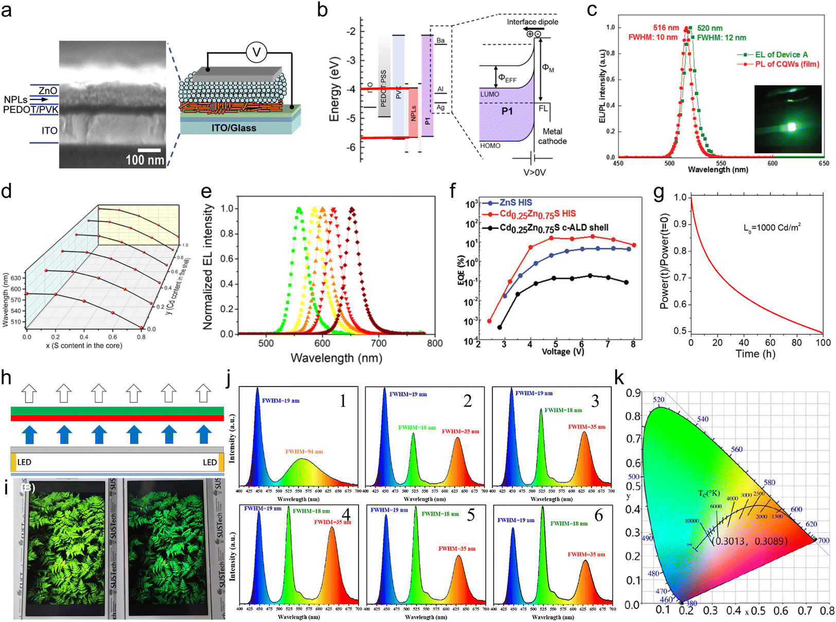 | ||
| Fig. 21 (a) Structure diagram (right) and the corresponding cross-sectional SEM image (left) of an NPL-LED device. Reproduced from ref. 21 with permission from Wiley-VCH copyright 2013. (b) Flat-band energy level diagram of the device with a polyelectrolytic polymer as the ETL. Reproduced from ref. 257 with permission from American Chemical Society, copyright 2018. (c) PL and electroluminescence (EL) spectra of CdSe NPLs. Inset: a photograph of an operating LED device. Reproduced from ref. 258 with permission from Wiley-VCH copyright 2019. (d) CdSe/ZnS NPL wavelength shift as a function of core alloying and shell alloying. (e) Tunable EL spectra at 1000 cd m−2 of NPLs with green, yellow, orange, red and deep-red emitters. Reproduced from ref. 79 with permission from American Chemical Society, copyright 2020. (f) EQE of NPL-LEDs with varying shell compositions. Reproduced from ref. 18 with permission from Wiley-VCH copyright 2019. (g) Normalized light power as a function of time at an initial luminance of 1000 cd m−2. Reproduced from ref. 259 with permission from American Chemical Society, copyright 2020. (h) Device structure of assembled backlight unit. (i) Display performance of screen with normal backlight unit (left) and assembly backlight unit (right). (j) Fluorescence spectrum of backlight using a blue LED chip with different films. Reproduced from ref. 260 with permission from Society for Information Display, copyright 2019. (k) CIE coordinates of Mn2+ doped CsPbBr3 NPLs. Reproduced from ref. 261 with permission from American Chemical Society, copyright 2021. | ||
With the continuous and in-depth exploration of the synthesis of NPLs, especially in the alloying of the core and shell, important breakthroughs in device performance have been achieved. Liu et al.258 demonstrated an ultra-pure green CdSe/CdS NPL-LED with an FWHM of only 12 nm corresponding to the CIE 1931 coordinates of (0.103, 0.797), which is slightly broadened compared to the PL spectrum (FWHM = 10 nm) (Fig. 21c). They further induced double emissions by doping Cu+ into CdSe/CdS NPLs and combined the Cu+ doped CdSe/CdS NPLs with blue ZnCdS/ZnS QDs to realize efficient white LEDs. Altintas et al.79 demonstrated spectrally tunable CdSe1−xSx/CdyZn1−yS NPL-LEDs in the range of 558 nm to 652 nm by systematically studying alloying mechanisms on both CdSe core and ZnS shell (Fig. 21d), the shell Cd-alloying results in shifting the emission from orange to red and only the core S-alloying causes a shift from orange to green (Fig. 21e). In particular, the yellow LED gives a max. EQE of 5.5% and a max. luminance of 46900 cd m−2. Recently, Liu et al.18 synthesized CdSe/Cd0.25Zn0.75S NPLs with a near-unity PLQY (95% in solution & 87% in film) through a HIS growth strategy that can effectively reduce lattice mismatch at the interface of core and shell (Fig. 21f).80 The fabricated red LEDs exhibit a maximum EQE of 19.2%, and a luminance of 23490 cd m−2, representing a record efficiency of NPL-LEDs. In addition, the morphology of NPLs can also affect the material's EL performance, and it is found that the LEDs with the square NPLs show higher efficiency than rod-like and rectangular NPL-based LEDs, since square NPLs have a much better surface coverage, edge-down formation, and negligible stacking effect in the film.168,262
Although significant advances have been made in the device performance of NPL-LEDs including efficiency and color purity, the stability lags far behind those of QD based LEDs. Currently, the best operational lifetime of NPL-LEDs was reported by Qu et al.,259 who designed CdSe/Cd0.05Zn0.95S core/shell structured NPLs as an emitter of red LEDs in which the Zn-alloying CdS shell not only passivates the surface defects of the NPL core but also improves the carrier transport significantly, and thus an extrapolated device lifetime of 3160 hours at 1000 cd m−2 is achieved (Fig. 21g shows a lifetime of 100 hours at 1000 cd m−2). Moreover, the CsPbBr3 NPL-based LEDs achieved a remarkable blue EL efficiency of 2% by utilizing the short-ligand capped CsPbBr3 NPLs.121 Nevertheless, more efforts are still required to promote the stable operation of high-efficiency NPL-LEDs.
6.2 Backlight for liquid crystal display
Semiconductor NPLs are used for the backlight of LCDs due to their advantages in color quality. Fig. 21h shows the device structure of an assembled backlight unit, where a uniform blue light is emitted from a blue LED chip side-mounted in the light guide plate and diffuses by reflection, refraction, and diffraction of various functional layers. The stacked NPLs and QDs dispersed in polymer film absorb most of the blue light and convert it downward to green and red light to produce white light with red, green and blue (RGB) colors. The screen based on the assembled backlight unit can present a colorful display and give more details of the object's color. Thanks to the narrow FWHMs (8–12 nm) of the NPLs, the backlight unit screen displays a higher saturation and a more remarkable color reduction, as compared to the normal screen (Fig. 21i). By varying the ratios of RGB colors (Fig. 21j), the white emissions can be well adjusted, achieving an ultra-wide color gamut of 139.9% National Television System Committee (NTSC) and 104.5% Rec.2020 (ITU-R Recommendation BT.2020).260 Recently, Zhao et al.261 introduced MnBr2 in the synthesis process of CsPbBr3 NPLs to enhance the thermal stability and PLQYs; taking advantage of Br− can effectively passivate the halide vacancies on the surface of NPLs and the Mn2+ ions are doped into the crystal lattice to form a more stable [MnBr6] octahedron. Mn-doped CsPbBr3 NPLs exhibit dual-emission at 460 nm and 610 nm, respectively, of which the PLQY reaches 64.4% and the corresponding CIE coordinates are (0.225, 0.291). By mixing the Mn2+ doped CsPbBr3 NPLs with the green CsPbBr3 NCs, they realized a WLED with the CIE coordinates of (0.3013, 0.3089) (Fig. 21k), showing great potential for application in solid-state lighting and displays.2616.3 Lasing
Due to the large absorption cross-section, wide size-dependent bandgap tunability, high exciton oscillator strengths, spectrally narrow gain profiles, giant OG coefficient, lower AR and fast hot carrier relaxation processes, semiconductor NPLs show the superior OG performance. The NPLs can be dispersed in many organic solvents providing convenience and flexibility in device preparation, and the photons produced in the NPL based optical devices can be effectively confined within the NPL waveguide resulting from the high refractive index of the solid NPL film, which supports various cavity configurations. Based on these advantages, the lower pumping threshold in ASE and lasing for NPLs can be obtained.48,54,136,263 She et al.264 synthesized multi-color NPLs by changing vertical thickness or chemical composition. The ASEs from these NPLs cover the entire visible spectrum and exhibit low threshold values of 50 μJ cm−2, 17 μJ cm−2, 28 μJ cm−2 and 6 μJ cm−2 for blue, green, yellow and red ASE, respectively (Fig. 22a–d); the gain bandwidth of 0.22 eV and a gain lifetime of 140 ps are achieved based on red NPLs placed in optical cavities. The lateral size of NPLs does not affect the ASE threshold or gain saturation level since the ASE requires only biexciton states.265 The multiexciton recombination in NPLs is also largely independent on the lateral size due to the small difference in the gain saturation. However, the gain saturation becomes more apparent when Auger complexes compete with ASE at high fluences. The 5 ML CdSe NPL family will have higher gain saturation benefiting from the longer AR lifetime which helps to maintain the population of the two-exciton state.264 In additional to changing the vertical thickness, chemical composition can also realize the tunable ASE performance. Kelestemur et al.263 designed core/crown and core/shell heterostructures of CdSexS1−x alloyed core NPLs to adjust their bandgaps for achieving tunable OG. The CdSexS1−x NPLs exhibit gain thresholds of ASE is ∼53 μJ cm−2 (Fig. 22e).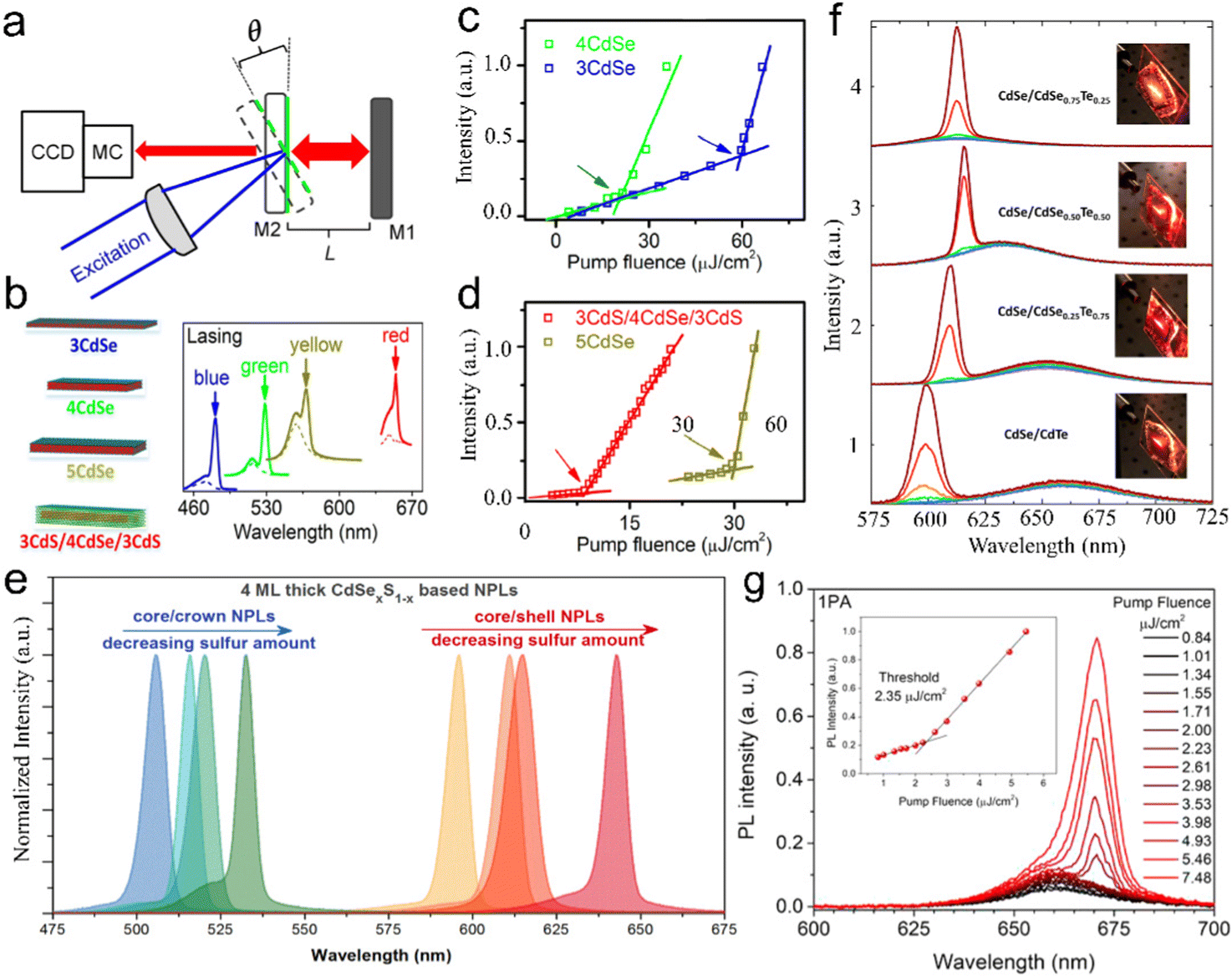 | ||
| Fig. 22 (a) Scheme of lasing measurements. Arrows indicate light propagation directions. (b) Schematics of CQWs with different vertical confinements, red (3CdS/4CdSe/3CdS), yellow (5CdSe), green (4CdSe), and blue (3CdSe) lasing spectra. (c) ASE threshold of green and blue emission CQWs. (d) ASE threshold of yellow and red emission CQWs. Reproduced from ref. 264 with permission from American Chemical Society, copyright 2015. (e) Normalized ASE spectra of CdSexS1−x/CdS alloyed CQWs showing highly tunable gain performance to cover the visible spectrum via changing the incorporated sulfur amount. The insets are the photos of the thin films when the pump intensity is above the ASE threshold. Reproduced from ref. 263 with permission from American Chemical Society, copyright 2017. (f) Emission spectra of the alloyed CdSe/CdSe1−xTex type-II core/crown NPLs with different x values when pump fluence is increased. Reproduced from ref. 266 with permission from American Chemical Society, copyright 2017. (g) An ultra-low ASE threshold of 2.35 mJ cm−2 of giant alloyed hot-injection CdSe/Cd0.25Zn0.75S core/shell CQWs. Reproduced from ref. 77 with permission from American Chemical Society, copyright 2019. | ||
Low-threshold gain of Type-II NPLs remained severely limited due to the shrinking oscillator strength and modest absorption cross-section. Borrowing the experiences from QDs, the researchers have utilized heterostructures or alloyed interfaces to reduce the OG threshold for NPLs. Guzelturk et al.266 design core/alloyed-crown CdSe/CdSexTe1−x NPL to prolong the gain lifetime to the nanosecond range (Fig. 22f). The excitation located in the alloyed crown region is electrically coupled to the charge transfer (CT) excitation at the type-II core/shell interface, which is responsible for the gain. The electronic coupling between the crown excitation and the CT state leads to a strong energy transfer and thus minimizes the reabsorption loss. As a result, the ASE of 26 μJ cm−2, OG lifetimes τgain ≈ 400 ps, and high modal gain coefficients gmodal ≈ 930 cm−1 are achieved.266 Altintas et al.77 utilized the HIS method to synthesize giant (ca. 4 nm thick) shelled CdSe/CdS NPLs. This method can reduce core/shell lattice mismatch, passivate surface defects, and regulate the distribution of carriers by changing the shell composition, resulting in the biexciton lifetime of CdSe/CdS NPL being prolonged to 1.26 ns, an order of magnitude longer than in conventional colloidal QDs.77 The core/alloyed-shell CdSe/CdZnS NPLs also exhibit a stable and low threshold OG of 2.35 μJ cm−2 and 0.83 mJ cm−2 under one- and two-photon pumping, respectively (Fig. 22g).
Taghipour et al.54 achieved OG thresholds in the sub-single exciton regime (N < 1) in the quasi-type II core/shell structured NPLs consisting of CdSe/CdS@Cd1−xZnxS core/crown@gradient alloyed shell NPL (Fig. 23a and b). The engineered NPLs have large absorption cross-section of 5.06 × 10⁻¹³ cm2, a large net modal gain coefficient of ∼1960 cm−1, and a long net OG lifetime of ∼830 ps, which leads to an ultra-low ASE threshold of 820 nJ cm−2, corresponding to an average number of 0.84 e–h pairs per NPL (Fig. 23c). The NPLs are then embedded in a Fabry–Pérot cavity and a lasing threshold of 7.46 mJ cm−2 is achieved (Fig. 23d). AR is suppressed in well-engineered NPLs with a biexciton Auger decay lifetime of 750 ± 50 ps; such a longer biexciton Auger lifetime is attributed to a significant reduction in the intraband transition strength due to smoother potential confinement.267 The fine grade of the confinement potential also contributes to the single exciton gain of the NPLs, which slows down the AR.267,268 Non-radiative multiexciton AR does not occur in this sub-exciton state, while the exact balance between absorption and excited emission is broken by the local electric field associated with the excited electron–hole pair, thus achieving population inversion and allowing OG to be displayed in the sub-single exciton state.269
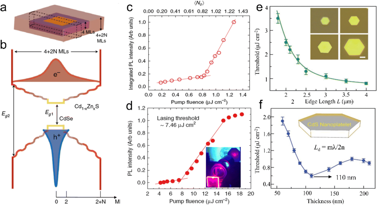 | ||
| Fig. 23 (a) Schematic illustration of CdSe/CdS@Cd1−xZnxS NPLs. (b) An approximate energy band diagram of the graded confinement potential in CdSe/CdS@Cd1−xZnxS NPLs. (c) Integrated PL intensity of ASE spectra as a function of the pump fluence and the corresponding average number of excitons per NPL. (d) PL emission intensity versus pump intensity (symbols). The red solid line indicates the lasing threshold of ∼7.46 μJ cm−2. Inset: photographical image of the CQW-based vertical-cavity surface-emitting (VCSEL) laser. Reproduced from ref. 54 with permission from Springer Nature, copyright 2020. (e) Lasing threshold as a function of the edge length of the hexagonal CdS NPLs. The olive curve is fitting to a 1/L2 relationship. Inset: the optical images of four hexagonal CdS NPLs with different edge lengths but comparable thicknesses of 90 ± 10 nm. Scale bar is 2 μm. (f) Thickness-dependent lasing threshold in hexagonal CdS NPLs with a similar edge length of 3.5 ± 0.2 μm and different thicknesses from 60 to 210 nm. Reproduced from ref. 270 with permission from Wiley-VCH copyright 2019. | ||
Low threshold micro/nanolasers using NPLs have attracted extensive attention, which shows great potential for applications in high-density storage and optical communication. Mi et al.270 utilized an initially self-limited epitaxial growth method to growth high-quality single-crystalline CdS NPLs with microscale lateral size and sub-wavelength vertical thickness. Hexagonal CdS whispering-gallery-mode (WGM) cavities are formed, and the WGM lasing exhibits an extremely lower threshold of 0.6 μJ cm−2, which is attributed to two important factors: (i) the highly crystalline CdS NPL microcavity suppresses a large amount of light loss, and (ii) the gain threshold of hexagonal CdS NPLs is much lower than the Fabry–Pérot mode of CdS NWs due to the strong mode constraint of the naturally formed WGM cavity. The relationship between the lasing threshold and NPL edge length (1/L2) indicates the laser performance of the hexagonal CdS cavity is mainly influenced by the planar WGM oscillations (Fig. 23e). Thickness-dependent lasing studies demonstrate the thresholds are partially affected by the vertical thickness of NPLs (Fig. 23f).270 Thanks to the effective passivation of the surface trap state and the suppression of exciton nonradiative complexes by growing high-quality CdS shells under high reaction temperatures, the PLQYs and photostability of ensemble CdSe/CdS NPLs are increased significantly. Meanwhile, the CdSe/CdS NPLs (6 MLs) film exhibits a conspicuous OG performance with a very low ASE threshold of 4.4 μJ cm−2, and the ultrafast transient dynamics process of ∼11 ps when the pump intensity was 13.2 μJ cm−2, long lifetime of >800 ps and large bandwidth of >140 nm of OG are observed. Moreover, the vertical-cavity surface-emitting laser was achieved with an ultralow lasing threshold of ∼1.1 μJ cm−2.271
7. Challenges and outlooks
This review provides in depth insights into atomically flat semiconductor NPLs from their synthesis to application. Due to the establishment of synthesis methodologies for NPLs, controllable morphologies and structures, such as thickness and lateral size, core/shell, core/crown and core/crown@shell, are achieved, which result in tunable emission wavelength and high PLQY. Benefiting from the ultra-narrow emission line width, short PL lifetime and high gain coefficient, high color purity, high EQE and low lasing threshold are achieved in the CdSe NPL-based light-emitting devices, including QLEDs, back-light for LEDs and lasers. Despite the huge progress in this field, some critical challenges are still urgent to be addressed in future research studies.The controlled synthesis of Cd-free NPLs: despite the huge progress in the synthesis of Cd-based NPLs, the presence of heavy metal cadmium hinders the further development of such NPLs. ZnSe, ZnTe and InP are environment friendly semiconductor materials. ZnSe, ZnTe and InP QDs have demonstrated outstanding optical properties across the visible region, which enable their application in achieving efficient QLEDs. However, the atomically flat ZnSe, ZnTe and InP NPLs with tunable thickness have not been achieved by the wet chemical methods, because the synthesis methods based on CdSe NPLs are not suitable for ZnSe, ZnTe and InP NPLs. Inspired by the intrinsic instability induced growth and the synthesis method for 6 ML CdSe NPLs discussed above, novel small anionic ligands should be explored to enhance the energy difference of vertical and lateral growth, which may result in anisotropic growth of zinc blende ZnSe, ZnTe and InP NPLs. Under such circumstances, fast lateral growth will occur while vertical growth is very slow or even prohibited.
The efficiency of red LEDs based on NPLs reaches 19%. However, the performance of green and blue ones lags far behind. The effects of the shape such as lateral dimensions and thickness, and composition and growth control of the NPLs on the device performance must be further explored. The self-stacking in NPLs may also degrade the luminous performance, therefore more efforts should be made for controlling the oriented stacking of the nanosheets in the film in developing NPL film preparation methods. More importantly, NPL-LEDs still exhibit a poor operating lifetime compared to QLEDs or other commercial display technologies, and therefore a more in-depth investigation of the failure mechanism from both the material and device structure is urgently needed.
A key challenge for NPL-based laser devices is their short lifetime, limiting their practical application. The degradation of laser performance under continuous optical excitation is still very fast, and intensive exploration of the stability improvement of NPL materials should be done, such as through selecting more appropriate surface ligands, coating with more stable shells, and developing new synthesis strategies for NPLs. Moreover, the development of electrically pumped lasers with NPL emitters remains in its infancy stage. From a fundamental point of view, it is still a mystery how to balance the mobility difference between electron/hole injection, how to suppress AR in this high carrier density environment, and what role the energy transfer or CT plays in the carrier injection process.
Conflicts of interest
There are no conflicts to declare.Acknowledgements
This work was supported by the Hebrew University of Jerusalem – Zelman Cowen Academic Initiatives (ZCAI) Joint Projects 2021, Fellowship of China Postdoctoral Science Foundation (No. 2021M701062) and the National Natural Science Foundation of China (No. 51675322).References
- A. P. Alivisatos, Science, 1996, 271, 933–937 CrossRef CAS.
- J. Joo, J. S. Son, S. G. Kwon, J. H. Yu and T. Hyeon, J. Am. Chem. Soc., 2006, 128, 5632–5633 CrossRef CAS PubMed.
- S. Deka, A. Quarta, M. G. Lupo, A. Falqui, S. Boninelli, C. Giannini, G. Morello, M. De Giorgi, G. Lanzani, C. Spinella, R. Cingolani, T. Pellegrino and L. Manna, J. Am. Chem. Soc., 2009, 131, 2948–2958 CrossRef CAS PubMed.
- P. Li, L. Wang, L. Wang and Y. Li, Chem. – Eur. J., 2008, 14, 5951–5956 CrossRef CAS PubMed.
- M. R. Gao, Y. F. Xu, J. Jiang and S. H. Yu, Chem. Soc. Rev., 2013, 42, 2986–3017 RSC.
- A. L. Efros and L. E. Brus, ACS Nano, 2021, 15, 6192–6210 CrossRef CAS PubMed.
- Y. Shirasaki, G. J. Supran, M. G. Bawendi and V. Bulović, Nat. Photonics, 2012, 7, 13–23 CrossRef.
- M. Nasilowski, B. Mahler, E. Lhuillier, S. Ithurria and B. Dubertret, Chem. Rev., 2016, 116, 10934–10982 CrossRef CAS PubMed.
- J. Zhang, Y. Sun, S. Ye, J. Song and J. Qu, Chem. Mater., 2020, 32, 9490–9507 CrossRef CAS.
- K. Wu and T. Lian, Chem. Soc. Rev., 2016, 45, 3781–3810 RSC.
- A. C. Berends and C. de Mello Donega, J. Phys. Chem. Lett., 2017, 8, 4077–4090 CrossRef CAS PubMed.
- A. Handelman, P. Beker, N. Amdursky and G. Rosenman, Phys. Chem. Chem. Phys., 2012, 14, 6391–6408 RSC.
- F. T. Rabouw and C. de Mello Donega, Top. Curr. Chem., 2016, 374, 58 CrossRef PubMed.
- T. Edvinsson, R. Soc. Open. Sci., 2018, 5, 180387 CrossRef CAS PubMed.
- J. J. Li, Y. A. Wang, W. Z. Guo, J. C. Keay, T. D. Mishima, M. B. Johnson and X. G. Peng, J. Am. Chem. Soc., 2003, 125, 12567–12575 CrossRef CAS PubMed.
- S. Kim, J.-A. Kim, T. Kim, H. Chung, S. Park, S.-M. Choi, H.-M. Kim, D.-Y. Chung and E. Jang, Chem. Mater., 2020, 32, 5200–5207 CrossRef CAS.
- X. Peng, J. Wickham and A. P. Alivisatos, J. Am. Chem. Soc., 1998, 120, 5343–5344 CrossRef CAS.
- B. Liu, Y. Altintas, L. Wang, S. Shendre, M. Sharma, H. Sun, E. Mutlugun and H. V. Demir, Adv. Mater., 2020, 32, 1905824 CrossRef CAS PubMed.
- F. Fan, P. Kanjanaboos, M. Saravanapavanantham, E. Beauregard, G. Ingram, E. Yassitepe, M. M. Adachi, O. Voznyy, A. K. Johnston, G. Walters, G. H. Kim, Z. H. Lu and E. H. Sargent, Nano Lett., 2015, 15, 4611–4615 CrossRef CAS PubMed.
- B. Liu, S. Delikanli, Y. Gao, D. Dede, K. Gungor and H. V. Demir, Nano Energy, 2018, 47, 115–122 CrossRef CAS.
- Z. Y. Chen, B. Nadal, B. Mahler, H. Aubin and B. Dubertret, Adv. Funct. Mater., 2014, 24, 295–302 CrossRef CAS.
- S. Hu, F. Shabani, B. Liu, L. Zhang, M. Guo, G. Lu, Z. Zhou, J. Wang, J. C. Huang, Y. Min, Q. Xue, H. V. Demir and C. Liu, ACS Nano, 2022, 16, 10840–10851 CrossRef CAS PubMed.
- S. Ithurria, M. D. Tessier, B. Mahler, R. P. Lobo, B. Dubertret and A. L. Efros, Nat. Mater., 2011, 10, 936–941 CrossRef CAS PubMed.
- J. S. Son, K. Park, S. G. Kwon, J. Yang, M. K. Choi, J. Kim, J. H. Yu, J. Joo and T. Hyeon, Small, 2012, 8, 2394–2402 CrossRef CAS PubMed.
- Z. Li, H. Qin, D. Guzun, M. Benamara, G. Salamo and X. Peng, Nano Res., 2012, 5, 337–351 CrossRef CAS.
- S. Ithurria and B. Dubertret, J. Am. Chem. Soc., 2008, 130, 16504–16505 CrossRef CAS PubMed.
- J. S. Son, X. D. Wen, J. Joo, J. Chae, S. I. Baek, K. Park, J. H. Kim, K. An, J. H. Yu, S. G. Kwon, S. H. Choi, Z. Wang, Y. W. Kim, Y. Kuk, R. Hoffmann and T. Hyeon, Angew. Chem., Int. Ed., 2009, 48, 6861–6864 CrossRef CAS PubMed.
- S. Ithurria, G. Bousquet and B. Dubertret, J. Am. Chem. Soc., 2011, 133, 3070–3077 CrossRef CAS PubMed.
- Z. Li and X. Peng, J. Am. Chem. Soc., 2011, 133, 6578–6586 CrossRef CAS PubMed.
- Y. H. Liu, F. Wang, Y. Wang, P. C. Gibbons and W. E. Buhro, J. Am. Chem. Soc., 2011, 133, 17005–17013 CrossRef CAS PubMed.
- S. Pedetti, B. Nadal, E. Lhuillier, B. Mahler, C. Bouet, B. Abécassis, X. Xu and B. Dubertret, Chem. Mater., 2013, 25, 2455–2462 CrossRef CAS.
- R. B. Vasiliev, E. P. Lazareva, D. A. Karlova, A. V. Garshev, Y. Yao, T. Kuroda, A. M. Gaskov and K. Sakoda, Chem. Mater., 2018, 30, 1710–1717 CrossRef CAS.
- H. Sun, F. Wang and W. E. Buhro, ACS Nano, 2018, 12, 12393–12400 CrossRef CAS PubMed.
- L. Dai, R. Lesyuk, A. Karpulevich, A. Torche, G. Bester and C. Klinke, J. Phys. Chem. Lett., 2019, 10, 3828–3835 CrossRef CAS PubMed.
- L. Dai, C. Strelow, T. Kipp, A. Mews, I. Benkenstein, D. Eifler, T. H. Vuong, J. Rabeah, J. McGettrick, R. Lesyuk and C. Klinke, Chem. Mater., 2020, 33, 275–284 CrossRef.
- H. Park, H. Chung and W. Kim, Mater. Lett., 2013, 99, 172–175 CrossRef CAS.
- P. D. Cunningham, I. Coropceanu, K. Mulloy, W. Cho and D. V. Talapin, ACS Nano, 2020, 14, 3847–3857 CrossRef CAS PubMed.
- Y. Pang, M. Zhang, D. Chen, W. Chen, F. Wang, S. J. Anwar, M. Saunders, M. R. Rowles, L. Liu, S. Liu, A. Sitt, C. Li and G. Jia, J. Phys. Chem. Lett., 2019, 10, 3465–3471 CrossRef CAS PubMed.
- F. Wang, M. Y. Zhang, W. Chen, S. Javaid, H. Yang, S. Wang, X. Y. Yang, L. C. Zhang, M. A. Buntine, C. S. Li and G. H. Jia, Nanoscale Adv., 2020, 2, 3316–3322 RSC.
- W. Cho, S. Kim, I. Coropceanu, V. Srivastava, B. T. Diroll, A. Hazarika, I. Fedin, G. Galli, R. D. Schaller and D. V. Talapin, Chem. Mater., 2018, 30, 6957–6960 CrossRef CAS.
- S. Christodoulou, J. I. Climente, J. Planelles, R. Brescia, M. Prato, B. Martin-Garcia, A. H. Khan and I. Moreels, Nano Lett., 2018, 18, 6248–6254 CrossRef CAS PubMed.
- S. Delikanli, G. Yu, A. Yeltik, S. Bose, T. Erdem, J. Yu, O. Erdem, M. Sharma, V. K. Sharma, U. Quliyeva, S. Shendre, C. Dang, D. H. Zhang, T. C. Sum, W. Fan and H. V. Demir, Adv. Funct. Mater., 2019, 29, 1901028 CrossRef.
- Y. Li, X. Hou, X. Dai, Z. Yao, L. Lv, Y. Jin and X. Peng, J. Am. Chem. Soc., 2019, 141, 6448–6452 CrossRef CAS PubMed.
- Y. H. Won, O. Cho, T. Kim, D. Y. Chung, T. Kim, H. Chung, H. Jang, J. Lee, D. Kim and E. Jang, Nature, 2019, 575, 634–638 CrossRef CAS PubMed.
- T. Kim, K. H. Kim, S. Kim, S. M. Choi, H. Jang, H. K. Seo, H. Lee, D. Y. Chung and E. Jang, Nature, 2020, 586, 385–389 CrossRef CAS PubMed.
- S. Ithurria and D. V. Talapin, J. Am. Chem. Soc., 2012, 134, 18585–18590 CrossRef CAS PubMed.
- S. Pedetti, S. Ithurria, H. Heuclin, G. Patriarche and B. Dubertret, J. Am. Chem. Soc., 2014, 136, 16430–16438 CrossRef CAS PubMed.
- Y. Kelestemur, B. Guzelturk, O. Erdem, M. Olutas, K. Gungor and H. V. Demir, Adv. Funct. Mater., 2016, 26, 3570–3579 CrossRef CAS.
- A. Hazarika, I. Fedin, L. Hong, J. Guo, V. Srivastava, W. Cho, I. Coropceanu, J. Portner, B. T. Diroll, J. P. Philbin, E. Rabani, R. Klie and D. V. Talapin, J. Am. Chem. Soc., 2019, 141, 13487–13496 CrossRef CAS PubMed.
- D. Porotnikov and M. Zamkov, J. Phys. Chem. C, 2020, 124, 21895–21908 CrossRef CAS.
- B. T. Diroll, J. Mater. Chem. C, 2020, 8, 10628–10640 RSC.
- A. Dutta, A. Medda and A. Patra, J. Phys. Chem. C, 2020, 125, 20–30 CrossRef.
- B. Guzelturk, M. Pelton, M. Olutas and H. V. Demir, Nano Lett., 2019, 19, 277–282 CrossRef CAS PubMed.
- N. Taghipour, S. Delikanli, S. Shendre, M. Sak, M. Li, F. Isik, I. Tanriover, B. Guzelturk, T. C. Sum and H. V. Demir, Nat. Commun., 2020, 11, 3305 CrossRef CAS PubMed.
- L. T. Kunneman, M. D. Tessier, H. Heuclin, B. Dubertret, Y. V. Aulin, F. C. Grozema, J. M. Schins and L. D. A. Siebbeles, J. Phys. Chem. Lett., 2013, 4, 3574–3578 CrossRef CAS.
- C. She, I. Fedin, D. S. Dolzhnikov, A. Demortiere, R. D. Schaller, M. Pelton and D. V. Talapin, Nano Lett., 2014, 14, 2772–2777 CrossRef CAS PubMed.
- J. Liu, L. Guillemeney, B. Abecassis and L. Coolen, Nano Lett., 2020, 20, 3465–3470 CrossRef CAS PubMed.
- C. E. Rowland, I. Fedin, H. Zhang, S. K. Gray, A. O. Govorov, D. V. Talapin and R. D. Schaller, Nat. Mater., 2015, 14, 484–489 CrossRef CAS PubMed.
- A. Medda, A. Dutta, S. Sain, S. Ghosh, I. Sarkar and A. Patra, J. Phys. Chem. C, 2022, 126, 7739–7747 CrossRef CAS.
- A. Dutta, A. Medda, S. Ghosh, S. Sain and A. Patra, ACS Appl. Nano Mater., 2022, 5, 11679–11688 CrossRef CAS.
- A. Riedinger, F. D. Ott, A. Mule, S. Mazzotti, P. N. Knusel, S. J. P. Kress, F. Prins, S. C. Erwin and D. J. Norris, Nat. Mater., 2017, 16, 743–748 CrossRef CAS PubMed.
- J. Joo, J. S. Son, S. G. Kwon, J. H. Yu and T. Hyeon, J. Am. Chem. Soc., 2006, 128, 5632–5633 CrossRef CAS PubMed.
- Y. H. Liu, V. L. Wayman, P. C. Gibbons, R. A. Loomis and W. E. Buhro, Nano Lett., 2010, 10, 352–357 CrossRef CAS PubMed.
- Y. Zhang, H. Zhang, D. Chen, C. J. Sun, Y. Ren, J. Jiang, L. Wang, Z. Li and X. Peng, Nano Lett., 2021, 21, 5201–5208 CrossRef CAS PubMed.
- A. H. Khan, R. Brescia, A. Polovitsyn, I. Angeloni, B. Martín-García and I. Moreels, Chem. Mater., 2017, 29, 2883–2889 CrossRef CAS.
- F. Manteiga Vazquez, Q. Yu, L. F. Klepzig, L. D. A. Siebbeles, R. W. Crisp and J. Lauth, J. Phys. Chem. Lett., 2021, 12, 680–685 CrossRef CAS PubMed.
- Q. A. Akkerman, B. Martín-García, J. Buha, G. Almeida, S. Toso, S. Marras, F. Bonaccorso, U. Petralanda, I. Infante and L. Manna, Chem. Mater., 2019, 31, 8145–8153 CrossRef CAS.
- Y. Yang, J. Li, L. Lin and X. Peng, Nano Res., 2015, 8, 3353–3364 CrossRef CAS.
- C. Pu, J. Zhou, R. Lai, Y. Niu, W. Nan and X. Peng, Nano Res., 2013, 6, 652–670 CrossRef CAS.
- A. Di Giacomo, C. Roda, A. H. Khan and I. Moreels, Chem. Mater., 2020, 32, 9260–9267 CrossRef CAS PubMed.
- M. D. Tessier, B. Mahler, B. Nadal, H. Heuclin, S. Pedetti and B. Dubertret, Nano Lett., 2013, 13, 3321–3328 CrossRef CAS PubMed.
- F. V. Antolinez, F. T. Rabouw, A. A. Rossinelli, J. Cui and D. J. Norris, Nano Lett., 2019, 19, 8495–8502 CrossRef CAS PubMed.
- M. D. Tessier, P. Spinicelli, D. Dupont, G. Patriarche, S. Ithurria and B. Dubertret, Nano Lett., 2014, 14, 207–213 CrossRef CAS PubMed.
- C. Meerbach, C. Wu, S. C. Erwin, Z. Dang, A. Prudnikau and V. Lesnyak, Chem. Mater., 2019, 32, 566–574 CrossRef.
- A. A. Rossinelli, A. Riedinger, P. Marques-Gallego, P. N. Knusel, F. V. Antolinez and D. J. Norris, Chem. Commun., 2017, 53, 9938–9941 RSC.
- B. Mahler, B. Nadal, C. Bouet, G. Patriarche and B. Dubertret, J. Am. Chem. Soc., 2012, 134, 18591–18598 CrossRef CAS PubMed.
- Y. Altintas, K. Gungor, Y. Gao, M. Sak, U. Quliyeva, G. Bappi, E. Mutlugun, E. H. Sargent and H. V. Demir, ACS Nano, 2019, 13, 10662–10670 CrossRef CAS PubMed.
- A. A. Rossinelli, H. Rojo, A. S. Mule, M. Aellen, A. Cocina, E. De Leo, R. Schäublin and D. J. Norris, Chem. Mater., 2019, 31, 9567–9578 CrossRef.
- Y. Altintas, B. Liu, P. L. Hernández-Martínez, N. Gheshlaghi, F. Shabani, M. Sharma, L. Wang, H. Sun, E. Mutlugun and H. V. Demir, Chem. Mater., 2020, 32, 7874–7883 CrossRef CAS.
- Y. Altintas, U. Quliyeva, K. Gungor, O. Erdem, Y. Kelestemur, E. Mutlugun, M. V. Kovalenko and H. V. Demir, Small, 2019, 15, 1804854 CrossRef PubMed.
- S. Shendre, S. Delikanli, M. Li, D. Dede, Z. Pan, S. T. Ha, Y. H. Fu, P. L. Hernandez-Martinez, J. Yu, O. Erdem, A. I. Kuznetsov, C. Dang, T. C. Sum and H. V. Demir, Nanoscale, 2018, 11, 301–310 RSC.
- A. H. Khan, G. H. V. Bertrand, A. Teitelboim, M. C. Sekhar, A. Polovitsyn, R. Brescia, J. Planelles, J. I. Climente, D. Oron and I. Moreels, ACS Nano, 2020, 14, 4206–4215 CrossRef CAS PubMed.
- C. Ben Mahmoud, A. Anelli, G. Csányi and M. Ceriotti, Phys. Rev. B, 2020, 102, 235130 CrossRef CAS.
- J. W. Robinson, Atomic Spectroscopy, CRC Press, 1996 Search PubMed.
- W. Demtröder, Laser Spectroscopy: Basic Concepts and Instrumentation, Springer Science & Business Media, 2013 Search PubMed.
- S. Ithurria, M. D. Tessier, B. Mahler, R. P. S. M. Lobo, B. Dubertret and A. L. Efros, Nat. Mater., 2011, 10, 936–941 CrossRef CAS PubMed.
- S. Christodoulou, J. I. Climente, J. Planelles, R. Brescia, M. Prato, B. Martín-García, A. H. Khan and I. Moreels, Nano Lett., 2018, 18, 6248–6254 CrossRef CAS PubMed.
- Q. Li, Q. Liu, R. D. Schaller and T. Lian, J. Phys. Chem. Lett., 2019, 10, 1624–1632 CrossRef CAS PubMed.
- Z. Hens and I. Moreels, J. Mater. Chem., 2012, 22, 10406–10415 RSC.
- D. Giovanni, W. K. Chong, H. A. Dewi, K. Thirumal, I. Neogi, R. Ramesh, S. Mhaisalkar, N. Mathews and T. C. Sum, Sci. Adv., 2016, 2, 1600477 CrossRef PubMed.
- Z. Hens and I. Moreels, J. Mater. Chem., 2012, 22, 10406–10415 RSC.
- P. Geiregat, C. Rodá, I. Tanghe, S. Singh, A. Di Giacomo, D. Lebrun, G. Grimaldi, J. Maes, D. Van Thourhout, I. Moreels, A. J. Houtepen and Z. Hens, Light: Sci. Appl., 2021, 10, 112 CrossRef CAS PubMed.
- J. Feldmann, G. Peter, E. O. Göbel, P. Dawson, K. Moore, C. Foxon and R. J. Elliott, Phys. Rev. Lett., 1987, 59, 2337–2340 CrossRef CAS PubMed.
- X. Xu, H. He, J. Li, Z. Fang, L. Gan, L. Chen and Z. Ye, ACS Appl. Mater. Interfaces, 2019, 11, 8436–8442 CrossRef CAS PubMed.
- C. Murray, D. J. Norris and M. G. Bawendi, J. Am. Chem. Soc., 1993, 115, 8706–8715 CrossRef CAS.
- N. Pradhan, D. Goorskey, J. Thessing and X. Peng, J. Am. Chem. Soc., 2005, 127, 17586–17587 CrossRef CAS PubMed.
- C. B. Murray, C. R. Kagan and M. G. Bawendi, Annu. Rev. Mater. Sci., 2000, 30, 545–610 CrossRef CAS.
- M. D. Tessier, C. Javaux, I. Maksimovic, V. Loriette and B. Dubertret, ACS Nano, 2012, 6, 6751–6758 CrossRef CAS PubMed.
- S. G. Kwon and T. Hyeon, Acc. Chem. Res., 2008, 41, 1696–1709 CrossRef CAS PubMed.
- A. Prudnikau, A. Chuvilin and M. Artemyev, J. Am. Chem. Soc., 2013, 135, 14476–14479 CrossRef CAS PubMed.
- C. Bouet, B. Mahler, B. Nadal, B. Abecassis, M. D. Tessier, S. Ithurria, X. Xu and B. Dubertret, Chem. Mater., 2013, 25, 639–645 CrossRef CAS.
- T. Hyeon, S. S. Lee, J. Park, Y. Chung and H. Bin Na, J. Am. Chem. Soc., 2001, 123, 12798–12801 CrossRef CAS PubMed.
- J. Yang, J. S. Son, J. H. Yu, J. Joo and T. Hyeon, Chem. Mater., 2013, 25, 1190–1198 CrossRef CAS.
- L. Manna, L. W. Wang, R. Cingolani and A. P. Alivisatos, J. Phys. Chem. B, 2005, 109, 6183–6192 CrossRef CAS PubMed.
- X.-Q. Li and Y. Arakawa, Phys. Rev. B: Condens. Matter Mater. Phys., 1999, 60, 1915 CrossRef CAS.
- L. Kubie, L. A. King, M. E. Kern, J. R. Murphy, S. Kattel, Q. Yang, J. T. Stecher, W. D. Rice and B. A. Parkinson, ACS Nano, 2017, 11, 8471–8477 CrossRef CAS PubMed.
- A. X. Wang, W. J. Wang, J. Y. Chen, R. D. Mao, Y. P. Pang, Y. G. Li, W. Chen, D. C. Chen, D. R. Hao, B. J. Ni, M. Saunders and G. H. Jia, J. Phys. Chem. Lett., 2020, 11, 4990–4997 CrossRef CAS PubMed.
- H. Fu, D. Yang, D. Qiu, C. H. Yan, R. Cai, Y. Du and W. Tan, J. Phys. Chem. Lett., 2022, 13, 1855–1862 CrossRef CAS PubMed.
- R. L. Penn and J. F. Banfield, Science, 1998, 281, 969–971 CrossRef CAS PubMed.
- C. Schliehe, B. H. Juarez, M. Pelletier, S. Jander, D. Greshnykh, M. Nagel, A. Meyer, S. Foerster, A. Kornowski, C. Klinke and H. Weller, Science, 2010, 329, 550–553 CrossRef CAS PubMed.
- Y. Chen, D. Chen, Z. Li and X. Peng, J. Am. Chem. Soc., 2017, 139, 10009–10019 CrossRef CAS PubMed.
- E. Lhuillier, S. Pedetti, S. Ithurria, B. Nadal, H. Heuclin and B. Dubertret, Acc. Chem. Res., 2015, 48, 22–30 CrossRef CAS PubMed.
- E. Lhuillier, S. Pedetti, S. Ithurria, H. Heuclin, B. Nadal, A. Robin, G. Patriarche, N. Lequeux and B. Dubertret, ACS Nano, 2014, 8, 3813–3820 CrossRef CAS PubMed.
- P. N. Knusel, A. Riedinger, A. A. Rossinelli, F. D. Ott, A. S. Mule and D. J. Norris, Chem. Mater., 2020, 32, 3312–3319 CrossRef CAS.
- F. D. Ott, A. Riedinger, D. R. Ochsenbein, P. N. Knusel, S. C. Erwin, M. Mazzotti and D. J. Norris, Nano Lett., 2017, 17, 6870–6877 CrossRef CAS PubMed.
- N. Moghaddam, C. Dabard, M. Dufour, H. Po, X. Xu, T. Pons, E. Lhuillier and S. Ithurria, J. Am. Chem. Soc., 2021, 143, 1863–1872 CrossRef CAS PubMed.
- H. Sun and W. E. Buhro, Chem. Mater., 2020, 32, 5814–5826 CrossRef CAS.
- C. Ji and W. E. Buhro, Chem. Mater., 2020, 32, 5290–5300 CrossRef CAS.
- L. Protesescu, S. Yakunin, M. I. Bodnarchuk, F. Krieg, R. Caputo, C. H. Hendon, R. X. Yang, A. Walsh and M. V. Kovalenko, Nano Lett., 2015, 15, 3692–3696 CrossRef CAS PubMed.
- J. Luo, X. Wang, S. Li, J. Liu, Y. Guo, G. Niu, L. Yao, Y. Fu, L. Gao, Q. Dong, C. Zhao, M. Leng, F. Ma, W. Liang, L. Wang, S. Jin, J. Han, L. Zhang, J. Etheridge, J. Wang, Y. Yan, E. H. Sargent and J. Tang, Nature, 2018, 563, 541–545 CrossRef CAS PubMed.
- H. Wang, F. Ye, J. Sun, Z. Wang, C. Zhang, J. Qian, X. Zhang, W. C. H. Choy, X. W. Sun, K. Wang and W. Zhao, ACS Energy Lett., 2022, 7, 1137–1145 CrossRef CAS.
- X. Xiao, Y. Li and R. J. Xie, Nanoscale, 2020, 12, 9231–9239 RSC.
- I. Levchuk, P. Herre, M. Brandl, A. Osvet, R. Hock, W. Peukert, P. Schweizer, E. Spiecker, M. Batentschuk and C. J. Brabec, Chem. Commun., 2016, 53, 244–247 RSC.
- L. Dou, A. B. Wong, Y. Yu, M. Lai, N. Kornienko, S. W. Eaton, A. Fu, C. G. Bischak, J. Ma, T. Ding, N. S. Ginsberg, L. W. Wang, A. P. Alivisatos and P. Yang, Science, 2015, 349, 1518–1521 CrossRef CAS PubMed.
- M. C. Weidman, A. J. Goodman and W. A. Tisdale, Chem. Mater., 2017, 29, 5019–5030 CrossRef CAS.
- C. Otero-Martinez, J. Ye, J. Sung, I. Pastoriza-Santos, J. Perez-Juste, Z. Xia, A. Rao, R. L. Z. Hoye and L. Polavarapu, Adv. Mater., 2022, 34, 2107105 CrossRef CAS PubMed.
- J. Shamsi, Z. Dang, P. Bianchini, C. Canale, F. Di Stasio, R. Brescia, M. Prato and L. Manna, J. Am. Chem. Soc., 2016, 138, 7240–7243 CrossRef CAS PubMed.
- D. Zhang, Y. Yu, Y. Bekenstein, A. B. Wong, A. P. Alivisatos and P. Yang, J. Am. Chem. Soc., 2016, 138, 13155–13158 CrossRef CAS PubMed.
- M. C. Weidman, M. Seitz, S. D. Stranks and W. A. Tisdale, ACS Nano, 2016, 10, 7830–7839 CrossRef CAS PubMed.
- P. Tyagi, S. M. Arveson and W. A. Tisdale, J. Phys. Chem. Lett., 2015, 6, 1911–1916 CrossRef CAS PubMed.
- J. A. Sichert, Y. Tong, N. Mutz, M. Vollmer, S. Fischer, K. Z. Milowska, R. Garcia Cortadella, B. Nickel, C. Cardenas-Daw, J. K. Stolarczyk, A. S. Urban and J. Feldmann, Nano Lett., 2015, 15, 6521–6527 CrossRef CAS PubMed.
- A. Pan, B. He, X. Fan, Z. Liu, J. J. Urban, A. P. Alivisatos, L. He and Y. Liu, ACS Nano, 2016, 10, 7943–7954 CrossRef CAS PubMed.
- Y. Bekenstein, B. A. Koscher, S. W. Eaton, P. Yang and A. P. Alivisatos, J. Am. Chem. Soc., 2015, 137, 16008–16011 CrossRef CAS PubMed.
- H. Fang, W. Deng, X. Zhang, X. Xu, M. Zhang, J. Jie and X. Zhang, Nano Res., 2018, 12, 171–176 CrossRef.
- Z.-J. Li, E. Hofman, A. H. Davis, M. M. Maye and W. Zheng, Chem. Mater., 2018, 30, 3854–3860 CrossRef CAS.
- M. Olutas, B. Guzelturk, Y. Kelestemur, A. Yeltik, S. Delikanli and H. V. Demir, ACS Nano, 2015, 9, 5041–5050 CrossRef CAS PubMed.
- A. Yeltik, S. Delikanli, M. Olutas, Y. Kelestemur, B. Guzelturk and H. V. Demir, J. Phys. Chem. C, 2015, 119, 26768–26775 CrossRef CAS.
- M. Failla, F. García Flórez, B. B. V. Salzmann, D. Vanmaekelbergh, H. T. C. Stoof and L. D. A. Siebbeles, Phys. Rev. B, 2020, 102, 195405 CrossRef CAS.
- D.-E. Yoon, J. Lee, H. Yeo, J. Ryou, Y. K. Lee, Y.-H. Kim and D. C. Lee, Chem. Mater., 2021, 33, 4813–4820 CrossRef CAS.
- G. H. Bertrand, A. Polovitsyn, S. Christodoulou, A. H. Khan and I. Moreels, Chem. Commun., 2016, 52, 11975–11978 RSC.
- A. H. Davis, E. Hofman, K. Chen, Z. J. Li, A. Khammang, H. Zamani, J. M. Franck, M. M. Maye, R. W. Meulenberg and W. W. Zheng, Chem. Mater., 2019, 31, 2516–2523 CrossRef CAS.
- M. Sharma, K. Gungor, A. Yeltik, M. Olutas, B. Guzelturk, Y. Kelestemur, T. Erdem, S. Delikanli, J. R. McBride and H. V. Demir, Adv. Mater., 2017, 29, 201700821 CrossRef PubMed.
- R. Viswanatha, S. Brovelli, A. Pandey, S. A. Crooker and V. I. Klimov, Nano Lett., 2011, 11, 4753–4758 CrossRef CAS PubMed.
- S. C. Erwin, L. Zu, M. I. Haftel, A. L. Efros, T. A. Kennedy and D. J. Norris, Nature, 2005, 436, 91–94 CrossRef CAS PubMed.
- D. J. Norris, A. L. Efros and S. C. Erwin, Science, 2008, 319, 1776–1779 CrossRef CAS PubMed.
- D. Mocatta, G. Cohen, J. Schattner, O. Millo, E. Rabani and U. Banin, Science, 2011, 332, 77–81 CrossRef CAS PubMed.
- G. M. Dalpian and J. R. Chelikowsky, Phys. Rev. Lett., 2006, 96, 226802 CrossRef PubMed.
- J. Zhang, Q. Di, J. Liu, B. Bai, J. Liu, M. Xu and J. Liu, J. Phys. Chem. Lett., 2017, 8, 4943–4953 CrossRef CAS PubMed.
- J. Liu, Q. Zhao, J. L. Liu, Y. S. Wu, Y. Cheng, M. W. Ji, H. M. Qian, W. C. Hao, L. J. Zhang, X. J. Wei, S. G. Wang, J. T. Zhang, Y. Du, S. X. Dou and H. S. Zhu, Adv. Mater., 2015, 27, 2753–2761 CrossRef CAS PubMed.
- J. H. Yu, X. Liu, K. E. Kweon, J. Joo, J. Park, K. T. Ko, D. W. Lee, S. Shen, K. Tivakornsasithorn, J. S. Son, J. H. Park, Y. W. Kim, G. S. Hwang, M. Dobrowolska, J. K. Furdyna and T. Hyeon, Nat. Mater., 2010, 9, 47–53 CrossRef CAS PubMed.
- L. Yang, K. E. Knowles, A. Gopalan, K. E. Hughes, M. C. James and D. R. Gamelin, Chem. Mater., 2016, 28, 7375–7384 CrossRef CAS.
- B. Bai, M. Xu, J. Z. Li, S. P. Zhang, C. Qiao, J. J. Liu and J. T. Zhang, Adv. Funct. Mater., 2021, 31, 202100286 Search PubMed.
- A. Najafi, M. Sharma, S. Delikanli, A. Bhattacharya, J. R. Murphy, J. Pientka, A. Sharma, A. P. Quinn, O. Erdem, S. Kattel, Y. Kelestemur, M. V. Kovalenko, W. D. Rice, H. V. Demir and A. Petrou, J. Phys. Chem. Lett., 2021, 12, 2892–2899 CrossRef CAS PubMed.
- T. Galle, M. Kazes, R. Hubner, J. Lox, M. S. Khoshkhoo, L. Sonntag, R. Tietze, V. Sayevich, D. Oron, A. Koitzsch, V. Lesnyak and A. Eychmuller, Chem. Mater., 2019, 31, 5065–5074 CrossRef CAS.
- A. H. Khan, V. Pinchetti, I. Tanghe, Z. Y. Dang, B. Martin-Garcia, Z. Hens, D. Van Thourhout, P. Geiregat, S. Brovelli and I. Moreels, Chem. Mater., 2019, 31, 1450–1459 CrossRef CAS.
- M. Sharma, M. Olutas, A. Yeltik, Y. Kelestemur, A. Sharma, S. Delikanli, B. Guzelturk, K. Gungor, J. R. McBride and H. V. Demir, Chem. Mater., 2018, 30, 3265–3275 CrossRef CAS.
- W. Liu, Q. Lin, H. Li, K. Wu, I. Robel, J. M. Pietryga and V. I. Klimov, J. Am. Chem. Soc., 2016, 138, 14954–14961 CrossRef CAS PubMed.
- Z.-J. Li, E. Hofman, A. H. Davis, A. Khammang, J. T. Wright, B. Dzikovski, R. W. Meulenberg and W. Zheng, Chem. Mater., 2018, 30, 6400–6409 CrossRef CAS.
- L. Wu, Y. Wang, M. Kurashvili, A. Dey, M. Cao, M. Döblinger, Q. Zhang, J. Feldmann, H. Huang and T. Debnath, Angew. Chem., Int. Ed., 2022, 61, 202115852 Search PubMed.
- N. N. Schlenskaya, Y. Yao, T. Mano, T. Kuroda, A. V. Garshev, V. F. Kozlovskii, A. M. Gaskov, R. B. Vasiliev and K. Sakoda, Chem. Mater., 2017, 29, 579–586 CrossRef CAS.
- B. M. Saidzhonov, V. B. Zaytsev, A. A. Eliseev, A. Y. Grishko and R. B. Vasiliev, ACS Photonics, 2020, 7, 3188–3198 CrossRef CAS.
- M. Dufour, J. Qu, C. Greboval, C. Methivier, E. Lhuillier and S. Ithurria, ACS Nano, 2019, 13, 5326–5334 CrossRef CAS PubMed.
- E. M. Hutter, E. Bladt, B. Goris, F. Pietra, J. C. van der Bok, M. P. Boneschanscher, C. de Mello Donegá, S. Bals and D. Vanmaekelbergh, Nano Lett., 2014, 14, 6257–6262 CrossRef CAS PubMed.
- O. Erdem, K. Gungor, B. Guzelturk, I. Tanriover, M. Sak, M. Olutas, D. Dede, Y. Kelestemur and H. V. Demir, Nano Lett., 2019, 19, 4297–4305 CrossRef CAS PubMed.
- S. Jana, M. de Frutos, P. Davidson and B. Abecassis, Sci. Adv., 2017, 3, 1701483 CrossRef PubMed.
- M. D. Tessier, L. Biadala, C. Bouet, S. Ithurria, B. Abecassis and B. Dubertret, ACS Nano, 2013, 7, 3332–3340 CrossRef CAS PubMed.
- B. Abecassis, M. D. Tessier, P. Davidson and B. Dubertret, Nano Lett., 2014, 14, 710–715 CrossRef CAS PubMed.
- B. Guzelturk, O. Erdem, M. Olutas, Y. Kelestemur and H. V. Demir, ACS Nano, 2014, 8, 12524–12533 CrossRef CAS PubMed.
- A. Antanovich, A. Prudnikau, A. Matsukovich, A. Achtstein and M. Artemyev, J. Phys. Chem. C, 2016, 120, 5764–5775 CrossRef CAS.
- S. Jana, T. N. Phan, C. Bouet, M. D. Tessier, P. Davidson, B. Dubertret and B. Abecassis, Langmuir, 2015, 31, 10532–10539 CrossRef CAS PubMed.
- R. Momper, H. Zhang, S. Chen, H. Halim, E. Johannes, S. Yordanov, D. Braga, B. Blulle, D. Doblas, T. Kraus, M. Bonn, H. I. Wang and A. Riedinger, Nano Lett., 2020, 20, 4102–4110 CrossRef CAS PubMed.
- B. T. Diroll, W. Cho, I. Coropceanu, S. M. Harvey, A. Brumberg, N. Holtgrewe, S. A. Crooker, M. R. Wasielewski, V. B. Prakapenka, D. V. Talapin and R. D. Schaller, Nano Lett., 2018, 18, 6948–6953 CrossRef CAS PubMed.
- F. V. Antolinez, F. T. Rabouw, A. A. Rossinelli, R. C. Keitel, A. Cocina, M. A. Becker and D. J. Norris, Nano Lett., 2020, 20, 5814–5820 CrossRef CAS PubMed.
- W. D. Kim, D.-E. Yoon, D. Kim, S. Koh, W. K. Bae, W.-S. Chae and D. C. Lee, J. Phys. Chem. C, 2019, 123, 9445–9453 CrossRef CAS.
- F. Wang, Y. Wang, Y. H. Liu, P. J. Morrison, R. A. Loomis and W. E. Buhro, Acc. Chem. Res., 2015, 48, 13–21 CrossRef CAS PubMed.
- A. Dutta, A. Medda, R. Bera, K. Sarkar, S. Sain, P. Kumar and A. Patra, ACS Appl. Nano Mater., 2020, 3, 4717–4727 CrossRef CAS.
- S. Jia, C. Song, M. Xu, B. Bai, J. Liu, H. Rong and J. Zhang, J. Phys. Chem. Lett., 2021, 12, 3976–3982 CrossRef CAS PubMed.
- P. Reiss, M. Protiere and L. Li, Small, 2009, 5, 154–168 CrossRef CAS PubMed.
- S. M. George, Chem. Rev., 2010, 110, 111–131 CrossRef CAS PubMed.
- R. L. Puurunen, J. Appl. Phys., 2005, 97, 9 CrossRef.
- C. Greboval, E. Izquierdo, C. Livache, B. Martinez, M. Dufour, N. Goubet, N. Moghaddam, J. Qu, A. Chu, J. Ramade, H. Aubin, H. Cruguel, M. Silly, E. Lhuillier and S. Ithurria, Nanoscale, 2019, 11, 3905–3915 RSC.
- H. Sun and W. E. Buhro, ACS Nano, 2019, 13, 6982–6991 CrossRef CAS PubMed.
- A. Mitrofanov, A. Prudnikau, F. Di Stasio, N. Weiß, R. Hübner, A. M. Dominic, K. B. L. Borchert, V. Lesnyak and A. Eychmüller, Chem. Mater., 2021, 33, 7693–7702 CrossRef CAS.
- S. Yadav, A. Singh, L. Thulasidharan and S. Sapra, J. Phys. Chem. C, 2017, 122, 820–829 CrossRef.
- A. Hu, P. Bai, Y. Zhu, Z. Song, R. Wang, J. Zheng, Y. Yao, Q. Zhang, Z. Ding, P. Gao, X. Sui, X. Liu and Y. Gao, Adv. Opt. Mater., 2022, 10, 2200469 CrossRef CAS.
- A. Hu, P. Bai, Y. Zhu, Z. Tang, L. Xiao and Y. Gao, Small, 2022, 18, 2204120 CrossRef CAS PubMed.
- Y. Kelestemur, B. Guzelturk, O. Erdem, M. Olutas, T. Erdem, C. F. Usanmaz, K. Gungor and H. V. Demir, J. Phys. Chem. C, 2017, 121, 4650–4658 CrossRef CAS.
- S. Delikanli, B. Guzelturk, P. L. Hernandez-Martinez, T. Erdem, Y. Kelestemur, M. Olutas, M. Z. Akgul and H. V. Demir, Adv. Funct. Mater., 2015, 25, 4282–4289 CrossRef CAS.
- Y. Kelestemur, M. Olutas, S. Delikanli, B. Guzelturk, M. Z. Akgul and H. V. Demir, J. Phys. Chem. C, 2015, 119, 2177–2185 CrossRef CAS.
- S. Yadav, A. Singh and S. Sapra, J. Phys. Chem. C, 2017, 121, 27241–27246 CrossRef CAS.
- M. Dufour, V. Steinmetz, E. Izquierdo, T. Pons, N. Lequeux, E. Lhuillier, L. Legrand, M. Chamarro, T. Barisien and S. Ithurria, J. Phys. Chem. C, 2017, 121, 24816–24823 CrossRef CAS.
- M. Green, J. Org. Chem., 1995, 500, 127–148 CrossRef CAS.
- N. C. Anderson, M. P. Hendricks, J. J. Choi and J. S. Owen, J. Am. Chem. Soc., 2013, 135, 18536–18548 CrossRef CAS PubMed.
- H. Sun and W. E. Buhro, Chem. Mater., 2021, 33, 1683–1697 CrossRef CAS.
- W. Zhang, G. Chen, J. Wang, B. C. Ye and X. Zhong, Inorg. Chem., 2009, 48, 9723–9731 CrossRef CAS PubMed.
- H. T. Uyeda, I. L. Medintz, J. K. Jaiswal, S. M. Simon and H. Mattoussi, J. Am. Chem. Soc., 2005, 127, 3870–3878 CrossRef CAS PubMed.
- J. B. Blanco-Canosa, M. Wu, K. Susumu, E. Petryayeva, T. L. Jennings, P. E. Dawson, W. R. Algar and I. L. Medintz, Coord. Chem. Rev., 2014, 263, 101–137 CrossRef.
- T. Kodanek, H. M. Banbela, S. Naskar, P. Adel, N. C. Bigall and D. Dorfs, Nanoscale, 2015, 7, 19300–19309 RSC.
- D. Kechkeche, E. Cao, C. Grazon, F. Caschera, V. Noireaux, M. L. Baron Niel and B. Dubertret, ACS Appl. Mater. Interfaces, 2018, 10, 24739–24749 CrossRef CAS PubMed.
- H. Halim, J. Simon, I. Lieberwirth, V. Mailander, K. Koynov and A. Riedinger, J. Mater. Chem. B, 2020, 8, 146–154 RSC.
- S. J. Lim, D. R. McDougle, M. U. Zahid, L. Ma, A. Das and A. M. Smith, J. Am. Chem. Soc., 2016, 138, 64–67 CrossRef CAS PubMed.
- Q. Zhou, Y. Cho, S. Yang, E. A. Weiss, T. C. Berkelbach and P. Darancet, Nano Lett., 2019, 19, 7124–7129 CrossRef CAS PubMed.
- B. T. Diroll, Chem. Mater., 2020, 32, 5916–5923 CrossRef CAS.
- P. R. Brown, D. Kim, R. R. Lunt, N. Zhao, M. G. Bawendi, J. C. Grossman and V. Bulovic, ACS Nano, 2014, 8, 5863–5872 CrossRef CAS PubMed.
- E. Izquierdo, A. Robin, S. Keuleyan, N. Lequeux, E. Lhuillier and S. Ithurria, J. Am. Chem. Soc., 2016, 138, 10496–10501 CrossRef CAS PubMed.
- Y. Zhou, F. Wang and W. E. Buhro, J. Am. Chem. Soc., 2015, 137, 15198–15208 CrossRef CAS PubMed.
- A. Antanovich, A. W. Achtstein, A. Matsukovich, A. Prudnikau, P. Bhaskar, V. Gurin, M. Molinari and M. Artemyev, Nanoscale, 2017, 9, 18042–18053 RSC.
- M. D. Tessier, C. Javaux, I. Maksimovic, V. Loriette and B. Dubertret, ACS Nano, 2012, 6, 6751–6758 CrossRef CAS PubMed.
- J. C. van der Bok, D. M. Dekker, M. L. J. Peerlings, B. B. V. Salzmann and A. Meijerink, J. Phys. Chem. C, 2020, 124, 12153–12160 CrossRef CAS.
- B. Henderson and G. F. Imbusch, Optical Spectroscopy of Inorganic Solids, Oxford University Press, 2006 Search PubMed.
- G. B. Griffin, S. Ithurria, D. S. Dolzhnikov, A. Linkin, D. V. Talapin and G. S. Engel, J. Chem. Phys., 2013, 138, 014705 CrossRef PubMed.
- M. Liao, B. Shan and M. Li, J. Phys. Chem. C, 2021, 125, 21062–21069 CrossRef CAS.
- P. Dey, J. Paul, J. Bylsma, D. Karaiskaj, J. M. Luther, M. C. Beard and A. H. Romero, Solid State Commun., 2013, 165, 49–54 CrossRef CAS.
- S. Ayari, M. T. Quick, N. Owschimikow, S. Christodoulou, G. H. V. Bertrand, M. Artemyev, I. Moreels, U. Woggon, S. Jaziri and A. W. Achtstein, Nanoscale, 2020, 12, 14448–14458 RSC.
- Q. Li and T. Lian, Nano Lett., 2017, 17, 3152–3158 CrossRef CAS PubMed.
- Z. Hu, A. Singh, S. V. Goupalov, J. A. Hollingsworth and H. Htoon, Nanoscale, 2018, 10, 22861–22870 RSC.
- L. Peng, M. Otten, A. Hazarika, I. Coropceanu, M. Cygorek, G. P. Wiederrecht, P. Hawrylak, D. V. Talapin and X. Ma, Phys. Rev. Mater., 2020, 4, 056006 CrossRef CAS.
- L. Biadala, F. Liu, M. D. Tessier, D. R. Yakovlev, B. Dubertret and M. Bayer, Nano Lett., 2014, 14, 1134–1139 CrossRef CAS PubMed.
- E. V. Shornikova, L. Biadala, D. R. Yakovlev, V. F. Sapega, Y. G. Kusrayev, A. A. Mitioglu, M. V. Ballottin, P. C. M. Christianen, V. V. Belykh, M. V. Kochiev, N. N. Sibeldin, A. A. Golovatenko, A. V. Rodina, N. A. Gippius, A. Kuntzmann, Y. Jiang, M. Nasilowski, B. Dubertret and M. Bayer, Nanoscale, 2018, 10, 646–656 RSC.
- A. W. Achtstein, R. Scott, S. Kickhöfel, S. T. Jagsch, S. Christodoulou, G. H. V. Bertrand, A. V. Prudnikau, A. Antanovich, M. Artemyev, I. Moreels, A. Schliwa and U. Woggon, Phys. Rev. Lett., 2016, 116, 116802 CrossRef PubMed.
- A. F. Vong, S. Irgen-Gioro, Y. Wu and E. A. Weiss, Nano Lett., 2021, 21, 10040–10046 CrossRef CAS PubMed.
- E. V. Shornikova, D. R. Yakovlev, L. Biadala, S. A. Crooker, V. V. Belykh, M. V. Kochiev, A. Kuntzmann, M. Nasilowski, B. Dubertret and M. Bayer, Nano Lett., 2020, 20, 1370–1377 CrossRef CAS PubMed.
- Y. P. Varshni, Physica, 1967, 34, 149–154 CrossRef CAS.
- D. P. Morgan and D. F. Kelley, J. Phys. Chem. C, 2019, 123, 18665–18675 CrossRef CAS.
- A. M. Kelley, Condensed-Phase Molecular Spectroscopy and Photophysics, John Wiley & Sons, 2012 Search PubMed.
- A. W. Achtstein, A. Schliwa, A. Prudnikau, M. Hardzei, M. V. Artemyev, C. Thomsen and U. Woggon, Nano Lett., 2012, 12, 3151–3157 CrossRef CAS PubMed.
- L. T. Kunneman, J. M. Schins, S. Pedetti, H. Heuclin, F. C. Grozema, A. J. Houtepen, B. Dubertret and L. D. Siebbeles, Nano Lett., 2014, 14, 7039–7045 CrossRef CAS PubMed.
- Q. S. Chen, J. Wu, X. Y. Ou, B. L. Huang, J. Almutlaq, A. A. Zhumekenov, X. W. Guan, S. Y. Han, L. L. Liang, Z. G. Yi, J. Li, X. J. Xie, Y. Wang, Y. Li, D. Y. Fan, D. B. L. Teh, A. H. All, O. F. Mohammed, O. M. Bakr, T. Wu, M. Bettinelli, H. H. Yang, W. Huang and X. G. Liu, Nature, 2018, 561, 88–93 CrossRef CAS PubMed.
- Y. H. Zhang, R. J. Sun, X. Y. Qi, K. F. Fu, Q. S. Chen, Y. C. Ding, L. J. Xu, L. M. Liu, Y. Han, A. V. Malko, X. G. Liu, H. H. Yang, O. M. Bakr, H. Liu and O. F. Mohammed, ACS Nano, 2019, 13, 2520–2525 CrossRef CAS PubMed.
- A. W. Achtstein, A. Antanovich, A. Prudnikau, R. Scott, U. Woggon and M. Artemyev, J. Phys. Chem. C, 2015, 119, 20156–20161 CrossRef CAS.
- M. Pelton, J. J. Andrews, I. Fedin, D. V. Talapin, H. Leng and S. K. O’Leary, Nano Lett., 2017, 17, 6900–6906 CrossRef CAS PubMed.
- B. Abécassis, M. D. Tessier, P. Davidson and B. Dubertret, Nano Lett., 2014, 14, 710–715 CrossRef PubMed.
- R. Momper, H. Zhang, S. Chen, H. Halim, E. Johannes, S. Yordanov, D. Braga, B. Blülle, D. Doblas, T. Kraus, M. Bonn, H. I. Wang and A. Riedinger, Nano Lett., 2020, 20, 4102–4110 CrossRef CAS PubMed.
- Y. Gao, M. C. Weidman and W. A. Tisdale, Nano Lett., 2017, 17, 3837–3843 CrossRef CAS PubMed.
- J. Lakwicz, Principles of Fluorescence Spectroscopy, Springer US, Boston, MA, 2006.
- I. Hadar, G. B. Hitin, A. Sitt, A. Faust and U. Banin, J. Phys. Chem. Lett., 2013, 4, 502–507 CrossRef CAS PubMed.
- D. V. Talapin, R. Koeppe, S. Götzinger, A. Kornowski, J. M. Lupton, A. L. Rogach, O. Benson, J. Feldmann and H. Weller, Nano Lett., 2003, 3, 1677–1681 CrossRef CAS.
- F. Pisanello, L. Martiradonna, P. Spinicelli, A. Fiore, J. P. Hermier, L. Manna, R. Cingolani, E. Giacobino, M. De Vittorio and A. Bramati, Superlattices Microstruct., 2010, 47, 165–169 CrossRef CAS.
- L. Liu, S. Huang, L. Pan, L.-J. Shi, B. Zou, L. Deng and H. Zhong, Angew. Chem., Int. Ed., 2017, 56, 1780–1783 CrossRef CAS PubMed.
- S. A. Crooker, J. A. Hollingsworth, S. Tretiak and V. I. Klimov, Phys. Rev. Lett., 2002, 89, 186802 CrossRef CAS PubMed.
- T. Franzl, D. S. Koktysh, T. A. Klar, A. L. Rogach, J. Feldmann and N. Gaponik, Appl. Phys. Lett., 2004, 84, 2904–2906 CrossRef CAS.
- C. B. M. C. R. Kagan, M. Nirmal and M. G. Bawendi, Phys. Rev. Lett., 1996, 76, 1517–1520 CrossRef CAS PubMed.
- L. T. Kunneman, M. D. Tessier, H. Heuclin, B. Dubertret, Y. V. Aulin, F. C. Grozema, J. M. Schins and L. D. A. Siebbeles, J. Phys. Chem. Lett., 2013, 4, 3574–3578 CrossRef CAS.
- P. G. V. Patten, J. Phys. Chem. C, 2008, 112, 10622–10631 CrossRef.
- I. Moreels, Nat. Mater., 2015, 14, 464–465 CrossRef CAS PubMed.
- N. Taghipour, P. L. Hernandez Martinez, A. Ozden, M. Olutas, D. Dede, K. Gungor, O. Erdem, N. K. Perkgoz and H. V. Demir, ACS Nano, 2018, 12, 8547–8554 CrossRef CAS PubMed.
- A. Medda, A. Dutta, D. Bain, M. K. Mohanta, A. De Sarkar and A. Patra, J. Phys. Chem. C, 2020, 124, 19793–19801 CrossRef CAS.
- E. Cassette, R. D. Pensack, B. Mahler and G. D. Scholes, Nat. Commun., 2015, 6, 6086 CrossRef CAS PubMed.
- A. Dutta, A. Medda, R. Bera, A. Rawat, A. De Sarkar and A. Patra, J. Phys. Chem. C, 2020, 124, 26434–26442 CrossRef CAS.
- A. Singh, X. Li, V. Protasenko, G. Galantai, M. Kuno, H. Xing and D. Jena, Nano Lett., 2007, 7, 2999–3006 CrossRef CAS PubMed.
- H. Yuan, X. Liu, F. Afshinmanesh, W. Li, G. Xu, J. Sun, B. Lian, A. G. Curto, G. Ye, Y. Hikita, Z. Shen, S. C. Zhang, X. Chen, M. Brongersma, H. Y. Hwang and Y. Cui, Nat. Nanotechnol., 2015, 10, 707–713 CrossRef CAS PubMed.
- J. Hao, Y. Li, J. Miao, R. Liu, J. Li, H. Liu, Q. Wang, H. Liu, M. H. Delville, T. He, K. Wang, X. Zhu and J. Cheng, ACS Nano, 2020, 14, 10346–10358 CrossRef CAS PubMed.
- M. V. Mukhina, V. G. Maslov, A. V. Baranov, A. V. Fedorov and Y. K. Gun’ko, Nano Lett., 2015, 15, 2844–2851 CrossRef CAS PubMed.
- D. A. Kurtina, A. V. Garshev, I. S. Vasil’eva, V. V. Shubin, A. M. Gaskov and R. B. Vasiliev, Chem. Mater., 2019, 31, 9652–9663 CrossRef CAS.
- J. Hao, F. Zhao, Q. Wang, J. Lin, P. Chen, J. Li, D. Zhang, M. Chen, P. Liu, M.-H. Delville, T. He, J. Cheng and Y. Li, Adv. Opt. Mater., 2021, 9, 2101142 CrossRef CAS.
- X. Gao, X. Zhang, L. Zhao, P. Huang, B. Han, J. Lv, X. Qiu, S.-H. Wei and Z. Tang, Nano Lett., 2018, 18, 6665–6671 CrossRef CAS PubMed.
- U. Giovanella, M. Pasini, M. Lorenzon, F. Galeotti, C. Lucchi, F. Meinardi, S. Luzzati, B. Dubertret and S. Brovelli, Nano Lett., 2018, 18, 3441–3448 CrossRef CAS PubMed.
- B. Liu, M. Sharma, J. Yu, S. Shendre, C. Hettiarachchi, A. Sharma, A. Yeltik, L. Wang, H. Sun, C. Dang and H. V. Demir, Small, 2019, 15, 1901983 CrossRef PubMed.
- J. Qu, P. Rastogi, C. Greboval, C. Livache, M. Dufour, A. Chu, S. S. Chee, J. Ramade, X. Z. Xu, S. Ithurria and E. Lhuillier, ACS Appl. Mater. Interfaces, 2020, 12, 22058–22065 CrossRef CAS PubMed.
- Z. Wen, F. Fang, C. Zhang, S. Ding, J. Sun, H. Tang, B. Xu, K. Wang, K. L. Teo and X. W. Sun, J. Soc. Inf. Disp., 2019, 27, 587–596 CrossRef CAS.
- Y. Zhao, C. Xie, X. Zhang, K. Matras-Postolek and P. Yang, ACS Appl. Nano Mater., 2021, 4, 6223–6230 CrossRef CAS.
- W. K. Bae, Y. S. Park, J. Lim, D. Lee, L. A. Padilha, H. McDaniel, I. Robel, C. Lee, J. M. Pietryga and V. I. Klimov, Nat. Commun., 2013, 4, 2661 CrossRef PubMed.
- Y. Kelestemur, D. Dede, K. Gungor, C. F. Usanmaz, O. Erdem and H. V. Demir, Chem. Mater., 2017, 29, 4857–4865 CrossRef CAS.
- C. She, I. Fedin, D. S. Dolzhnikov, P. D. Dahlberg, G. S. Engel, R. D. Schaller and D. V. Talapin, ACS Nano, 2015, 9, 9475–9485 CrossRef CAS PubMed.
- J. Q. Grim, S. Christodoulou, F. Di Stasio, R. Krahne, R. Cingolani, L. Manna and I. Moreels, Nat. Nanotechnol., 2014, 9, 891–895 CrossRef CAS PubMed.
- B. Guzelturk, Y. Kelestemur, M. Olutas, Q. Li, T. Lian and H. V. Demir, J. Phys. Chem. Lett., 2017, 8, 5317–5324 CrossRef CAS PubMed.
- J. M. Pietryga, Y.-S. Park, J. Lim, A. F. Fidler, W. K. Bae, S. Brovelli and V. I. Klimov, Chem. Rev., 2016, 116, 10513–10622 CrossRef CAS PubMed.
- Y.-S. Park, W. K. Bae, T. Baker, J. Lim and V. I. Klimov, Nano Lett., 2015, 15, 7319–7328 CrossRef CAS PubMed.
- V. I. Klimov, S. A. Ivanov, J. Nanda, M. Achermann, I. Bezel, J. A. McGuire and A. Piryatinski, Nature, 2007, 447, 441–446 CrossRef CAS PubMed.
- Y. Mi, B. Jin, L. Zhao, J. Chen, S. Zhang, J. Shi, Y. Zhong, W. Du, J. Zhang, Q. Zhang, T. Zhai and X. Liu, Small, 2019, 15, 1901364 CrossRef PubMed.
- L. Zhang, H. Yang, B. Yu, Y. Tang, C. Zhang, X. Wang, M. Xiao, Y. Cui and J. Zhang, Adv. Opt. Mater., 2019, 8, 1901615 CrossRef.
Footnote |
| † These authors contributed equally to this work. |
| This journal is © The Royal Society of Chemistry 2023 |