
 Open Access Article
 This Open Access Article is licensed under a
 Creative Commons Attribution 3.0 Unported Licence
Unidirectional growth of epitaxial tantalum disulfide triangle crystals grown on sapphire by chemical vapour deposition with a separate-flow system†
Takashi
Yanase
 *a,
Miu
Ebashi
a,
Kotaro
Takamure
b,
Wataru
Ise
c,
Hiroki
Waizumi
c,
Akira
Chikamatsu
d,
Yasushi
Hirose
e and
Toshihiro
Shimada
c
*a,
Miu
Ebashi
a,
Kotaro
Takamure
b,
Wataru
Ise
c,
Hiroki
Waizumi
c,
Akira
Chikamatsu
d,
Yasushi
Hirose
e and
Toshihiro
Shimada
c
aDepartment of Chemistry, Faculty of Science, Toho University, 2-2-1 Miyama, Funabashi, Chiba 274-8510, Japan. E-mail: takashi.yanase@sci.toho-u.ac.jp
bInstitute of Materials and Systems for Sustainability, Division of Materials Research, Nagoya University, Furocho, Chikusa-ku, Nagoya, Aichi 464-8601, Japan
cDivision of Applied Chemistry, Faculty of Engineering, Hokkaido University, Kita 13 Nishi 8 Kita-ku, Sapporo, Hokkaido 060-8628, Japan
dDepartment of Chemistry, Faculty of Science, Ochanomizu University, 2-1-1 Otsuka, Bunkyo-ku, Tokyo 112-8610, Japan
eDepartment of Chemistry, Graduate School of Science, Tokyo Metropolitan University, 1-1 Minamiosawa Hachioji, Tokyo 192-0397, Japan
First published on 6th December 2023
Abstract
Tantalum disulfide has been attracting considerable attention due to its rich phase diagram that includes polytypes and charge density waves, thus having potential for electrical device applications. However, epitaxial TaS2 thin films grown by chemical vapour deposition are still limited due to few available precursors. Herein, an originally designed atmospheric chemical vapour deposition with a separate-flow system was proposed to accomplish the controlled synthesis of TaS2 thin films. The sophisticated deposition sequence enables us to make unidirectional TaS2 triangle domains on c-plane sapphire using a chloride precursor. The quality of the grown TaS2 thin films was confirmed by X-ray diffraction, Raman spectroscopy, transmission electron microscopy and observing a step-and-terrace structure without spiral defects. The growth mechanism was discussed and concluded as the Volmer–Weber mode from the surface morphologies and elemental analysis. Our strategy is expandable to the other transition metal dichalcogenides because all the chloride precursors show a considerable vapour pressure below 200 °C.
1 Introduction
Although mechanical exfoliation is still used for the fundamental study of two-dimensional materials,1–3 chemical vapour deposition (CVD) is one of the most reliable and scalable methods to synthesize two-dimensional transition metal dichalcogenides (TMDCs).4–17 Molybdenum dichalcogenides (MoX2)5,7–10,12,13,18 and tungsten dichalcogenides (WX2)4,6,19 of the TMDCs have been most extensively studied in the past decade due to the existence of a volatile oxide precursor. The high volatility of the oxide precursor can simplify CVD apparatus to synthesize epitaxially grown thin films of MoX2 and WX2, even a monolayer because oxide impurities are automatically eliminated from the product. Another advantage of MoX2 and WX2 is that oxygen gas can be used as an additive to keep the precursors fresh during the reaction.20,21 However, this strategy is not applicable to synthesize the other TMDCs since there is no corresponding volatile oxide precursor for the other transition metals. It is well-known that the salt-assisted CVD22–24 is helpful to increase the vapour pressure of the oxide precursor and to synthesize various TMDCs. However, it is not controllable because the salt is consumed during the reaction. Although metal–organic CVD6,25 is another route for the growth of TMDC films with good controllability and flexibility, the following disadvantages should be overcome: an expensive high vacuum system is required, and carbon impurities are simultaneously deposited. In addition, the water-assisted one-pot CVD method was recently developed to grow a wide range of MoX2, WX2, and their alloys.26–29 It can only apply to molybdenum and tungsten because the other transition metals form stable oxides if oxygen atoms exist in the precursor or carrier gas. Therefore, it is desirable to establish a cost-effective CVD with good controllability and flexibility to obtain epitaxially grown TMDC films with various transition metals.This study proposed an atmospheric pressure CVD (APCVD) with a separate-flow and computer-controlled system (see the Experimental section), which avoided the several weak points of the conventional single-flow APCVD. Among the various TMDCs, tantalum disulfide (TaS2) was selected in this study because high-quality epitaxial TaS2 films are significantly desirable for fundamental research and device applications from the viewpoint of the rich phase diagram, including polytypes and charge density waves (CDWs).30–32 However, it is still a great challenge to grow TaS2 films by CVD due to the limited available precursor. Herein, the epitaxial growth of highly-oriented TaS2 triangle flakes was successfully done on c-plane sapphire via the homemade APCVD using volatile TaCl5, elemental sulphur, and hydrogen. A flat and inert c-plane sapphire is favourable for the van der Waals epitaxy30 due to its 3-fold symmetry and is known to be valid for MoS2 (ref. 5) and WS2.6
We confirmed the epitaxial growth of unidirectional TaS2 flakes using optical microscopy (OM) and X-ray diffraction (XRD). Single crystallinity of a triangle domain was confirmed by transmission electron microscopy (TEM). The growth mechanism is discussed based on the surface morphology and elemental analysis of the epitaxial TaS2 flakes. Our CVD method is expandable to the growth of the other TMDCs and other layered materials,33–36 such as metal monochalcogenides, because most (transition) metal chlorides have sufficient vapour pressures below 200 °C. It is believed that our CVD system opens up the possibility of establishing a sophisticated way to synthesize various TMDC alloys and to carry out doping to control the electric conductivity.
2 Experimental
TaS2 thin films were synthesized using specially-designed APCVD apparatus with a separate-flow system partially modified from the original one.7,15,37 A schematic illustration of the APCVD is shown in Fig. 1. The apparatus comprises a furnace, a quartz tube with an inner diameter of 22 mm, and two source containers located far from the reaction zone (furnace). The source containers made of glass were connected to the quartz tube using stainless steel pipes and a Wilson seal. Each glass container can be independently heated using a pipe heater to precisely control the vapour pressures of the sources (see Fig. S1†). The supply lines of the sulphur vapour and TaCl5 vapour were called the sulphur line and TaCl5 line, respectively. The two lines were connected at the entrance of the quartz tube to finely mix the vapours before transferring them into the reaction zone. The dew point of the TaCl5 line upstream was measured and kept at lower than −60 °C to prevent the chloride source from oxidizing. Notably, our APCVD system had the following features that differed from the conventional single-flow CVD14,16,38–40 to improve controllability and reproducibility. (1) The supply amounts of the sulphur vapour and TaCl5 vapour could be independently controlled, while the conventional single-flow CVD cannot simultaneously optimize them. (2) The cross-contamination of the sources, which is inevitable in conventional CVD, was avoided by separately placing them from the reaction zone. (3) The flow rates of both lines were computer-controlled for the accurate supply of the source vapours. Although the authors recognized a different type of separate-flow system for the oxide precursor to be placed in the inner quartz tube, it is inappropriate for CVD using a chloride precursor due to the inevitable air exposure.5,13,21,37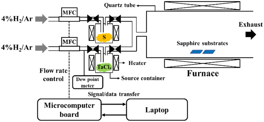 | ||
| Fig. 1 An APCVD with a separate-flow system for synthesizing epitaxial TaS2 films. All the parameters (the flow rates of the sulphur line and TaCl5 line, the temperatures of sulphur and TaCl5, and reaction temperature) were separately controlled. MFC represents a mass flow controller. | ||
TaCl5 powder (∼0.3 g, >95%, TCI Co., Ltd.) and S powder (∼0.3 g, Cica-Reagent, Kanto Chemical Co., Inc.) were introduced into the corresponding containers without further purification. TaCl5 powder should always be handled under an inert atmosphere; otherwise, it is easily oxidized and loses its volatility. Even when the source container was removed from the CVD system and placed in a glove box to refill the chloride source, air exposure was completely avoided by equipping the valves with containers. Note that TaCl5 could be repeatedly used at least five times if one carefully controls the handling and dew point of the TaCl5 line. The reusability of the source is essential for research efficiency and commercialization of the TaS2 thin films. The growth conditions to synthesize the TaS2 films were as follows: 6 × 6 mm2c-plane sapphire substrates were placed at the centre of the furnace. The furnace, TaCl5, and sulphur were heated at 900–950 °C, 145–160 °C and 210 °C, respectively. The flow rates of the TaCl5 line and sulphur line were set at 150 sccm and 350 sccm for 5 min. The detailed procedure of CVD is described in the ESI.† In addition, the sequence of the furnace temperature and the flow rates of the sulphur and TaCl5 lines are depicted in Fig. S2† for clarity. The sets of the growth parameters labelled with sample numbers (i)–(v) are also summarized in Table S1.†
The morphology of the grown films was observed by OM (Yashima TBR-1), atomic force microscopy (AFM, Hitachi High-Tech, AFM5000II with SPA400), scanning electron microscopy (SEM, JEOL, JSM-7100F) and TEM (JEOL, JEM-2010). The temperature gradient and convective flow of the CVD system were simulated by a computational fluid dynamics (CFD, SCRYU/Tetra) method. The vibrational modes were characterized by Raman spectroscopy (Renishaw Invia/JASCO NRS-5100) with 532 nm excitation. The crystallinity and orientation of the grown films were measured by XRD (Rigaku, MiniFlex, λ = 0.15418 nm) in the θ–2θ scan mode. Elemental analysis was carried out using an energy dispersive X-ray spectrometer (EDX) equipped with an SEM. X-ray photoemission spectroscopy (XPS, Thermo Fisher, Scientific K-Alpha) measurements were performed at 300 K using an Al Kα X-ray source to investigate the chemical state and the thickness of the native oxide. A charge-neutralizing flood gun was used to suppress the surface charge-up.
3 Results and discussion
It was crucial for the successful synthesis of the TaS2 thin films to minimize any traces of water and oxygen in the CVD system because the oxidation reaction is more favourable than the sulphurisation reaction.17,41 The Gibbs free energy of the reaction at 1200 K (∼927 °C) to form one mole of Ta2O5 reacted by water (ΔrG ∼ −535 kJ mol−1) or oxygen (ΔrG ∼ −577 kJ mol−1) is much lower than that of TaS2 (ΔrG ∼ −239 kJ mol−1).42 Therefore, the dew point of the TaCl5 line was kept at lower than −60 °C as mentioned in the Experimental section. Detailed thermodynamic calculations to obtain ΔrG are shown in the ESI.† Besides, the CVD sequence explained in the ESI† and Fig. S2, specifically the prior supply of the sulphur vapour before providing the chloride vapour, was essential for the epitaxial growth of TaS2. This is because the TaCl5 vapour can react with the sapphire substrate in the absence of sulphur vapour, which may result in a rough surface of sapphire and pyramidal crystal formation, as pointed out in the literature.17 A thermodynamic calculation also supports this argument as shown in the ESI.†The position of the sapphire substrates was also important in reproducing the results because the temperature gradient and convection in the quartz tube cannot be ignored. In order to visualize them, CFD simulations were performed in our CVD system (see the details of simulations in the ESI†). As shown in Fig. 2, a temperature gradient and convective flow at the reaction temperature of 925 °C exist even near the centre of the furnace, meaning that the sample position should always be the same to guarantee reproducibility. In particular, the convective flow is thought to be the dominant factor influencing the stability and reproducibility because the convective velocity right above the sapphire substrate (7.45 cm s−1) was higher than the average velocity in the quartz tube (2.193 cm s−1). The temperature gradient and convective flow at the reaction temperatures of 900 °C and 950 °C are also shown in Fig. S3.† Additionally, the temperature gradient and convective flow of the whole system are shown in Fig. S4.† Since the convection affects the mass transport of the TaCl5, S, and H2 molecules to the surface of the sapphire, it should be placed at the centre of the furnace to minimize the convection effect. A vertically aligned CVD19 should be used to remove the convection around the substrate in the near future.
 | ||
| Fig. 2 (a) Gas velocity around a sapphire substrate simulated at 925 °C by CFD. The velocity of the convective flow on the sapphire (7.45 cm s−1) is greater than the average velocity of 2.193 cm s−1, illustrating that convection affects the mass transport of the TaCl5, sulphur, and H2 molecules to the surface of the sapphire. (b) Side view and (c) cross-section of the temperature gradient around a sapphire substrate. A–C show the positions of the cross-section. The arrows show the gas velocity. A convective flow also exists on the cross section. | ||
Fig. 3(a)–(c) (that correspond to samples (i)–(iii)) show the OM images of the epitaxial TaS2 films grown on c-plane sapphire substrates at the TaCl5 temperature of 145, 150, and 160 °C, respectively. One can see that the domain size of the crystals increased from 2 to 15 mm as the amount of the TaCl5 vapour increased. The magnified AFM image of sample (i) is shown in Fig. 3(f) for the clarity of the triangle domains. SEM images of the corresponding labelled figures are also shown in Fig. S5.† These OM, AFM, and SEM observations indicate that the vapour pressure of TaCl5 is a critical parameter in determining the domain size. Notably, when the TaCl5 vapour was excessive, standing flakes were observed probably due to the short migration length of the adatoms on the substrate surface and frequent nucleation.19 This result shows the necessity of careful control of the amount of supplied TaCl5 vapour to obtain high-quality epitaxial films. After the temperature of TaCl5 was optimized at 150 °C, the growth temperature was varied from 950 to 900 °C. Surprisingly, most triangle domains were highly oriented along a specific direction when the growth temperature was 925 °C (Fig. 3(d)). It was found that the standing flakes were observed again when the growth temperature decreased to 900 °C (Fig. 3(e)) due to the same reason as for sample (iii). The orientation histogram shown in Fig. 4(b) was created by counting the isolated (not coalesced) triangular domains at the edge of the substrate as shown in Fig. 4(a). The way to create the orientation histogram is explained in Fig. S6.† The major triangular single domains (76% of isolated domains) were aligned with 0°, indicating unidirectional growth of the TaS2 thin films. A fraction of the domains with an angle of ±60° is 12% while the rest (12%) showed other orientations. Note that it is the first report of unidirectional growth of TaS2 films although such unidirectional growth was observed in the case of MoS2 (ref. 5 and 9) and WS2.6 From the viewpoint of symmetry of substrates and 2D materials, the number of equivalent directions with the minimum binding energy between the sapphire and TaS2 was calculated as 1 (ref. 43) primarily due to the 3-fold symmetry of the sapphire, which means that the unidirectional growth of TaS2 on sapphire is reasonable. The growth conditions must be carefully controlled; otherwise, the growth direction can be easily random due to the small rotation energy43 as seen in Fig. 3 and previous reports.18,44
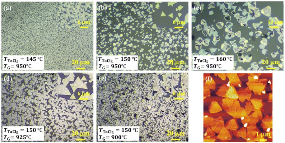 | ||
| Fig. 3 (a)–(e) OM images of epitaxially grown TaS2 films at various TaCl5 temperatures (TTaCl5) and growth temperatures (TG) (sample numbers (i)–(v)). The enlarged images at the centres of the individual ones are shown as insets to observe the shape of the domains. (f) Magnified AFM image of sample (a). | ||
 | ||
| Fig. 4 (a) OM image at the edge of the sapphire to count the isolated triangle domains. (b) Orientation histogram of TaS2 thin films showing the unidirectional growth. The inset shows the geometrical relationship between the original axis and measured theta (θ). | ||
Fig. 5(a) shows the XRD patterns of the grown films. The scale of the intensity was normalized with the (0 0 0 l) peaks to compare them. The diffraction peaks denoted as (0 0 0 l), (0 0 0 2 l), and (0 0 0 3 l) (l = 1 for 1T phase, l = 2 for 2H phase) were derived from the basal planes of TaS2 while the peaks at around 41.7 degrees originated from the c-plane sapphire substrates. It was confirmed that the interlayer distance (0.596 ± 0.002 nm) calculated from (0 0 0 l) is in reasonable agreement with the reported values of the bulk counterpart.45,46 The absence of a diffraction peak from the non-basal plane proved that most of the TaS2 flakes were epitaxially grown along the c-axis, consistent with the OM observation result. Furthermore, all the (0 0 0 l) diffraction peaks are sharp and intense, meaning the considerable good crystallinity of the films. The oxide phase is not seen in the XRD patterns, indicating that the surface oxide layer was scarcely present,47–51 consistent with the XPS spectra shown later. A TEM image and electron diffraction pattern were also obtained to confirm the crystallinity of the triangle domains as shown in Fig. 5(b) and (c). The perfect triangle is consistent with the result of the OM image. The hexagonal symmetry of the diffraction pattern reflects the high-quality single crystal. The d value estimated from the (10![[1 with combining macron]](https://www.rsc.org/images/entities/char_0031_0304.gif) 0) spots was 0.27 nm, which is in reasonable agreement with the reported value in the literature.16
0) spots was 0.27 nm, which is in reasonable agreement with the reported value in the literature.16
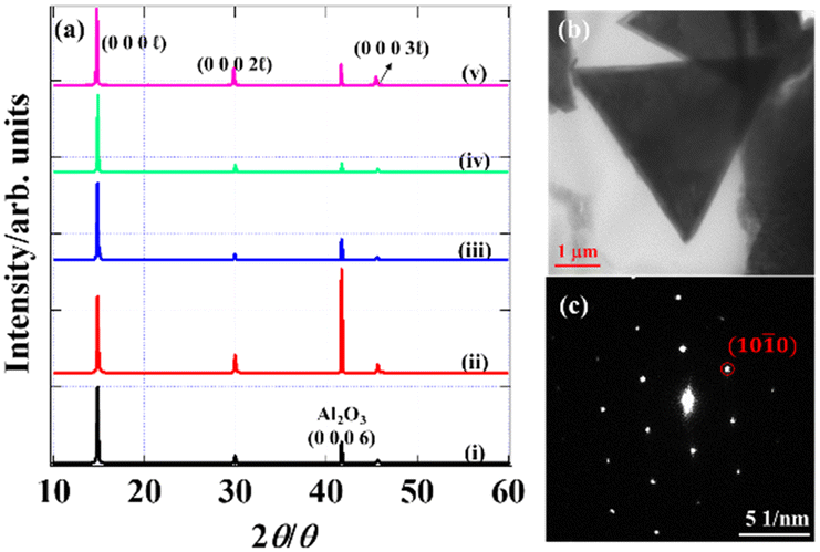 | ||
| Fig. 5 (a) XRD patterns of samples (i)–(v). Only the diffraction peaks that originated from the basal plane were observed and labelled (0 0 0 l), (0 0 0 2 l), and (0 0 0 3 l). The peaks at around 41.7 degrees originated from the c-plane sapphire substrates. The calculated interlayer distance (0.596 ± 0.002 nm) is consistent with the reported values. (b) TEM image of sample (iv). (c) Electron diffraction pattern of the triangle domain shown in (b). | ||
Although it is well-known that TaS2 has several polytypes, i.e., different coordination and stacking modes with the same chemical composition, it is risky to judge the phase of TaS2 only from the diffraction patterns48 of the epitaxially grown films because there is only a slight difference in the d values. However, Raman spectroscopy can adequately distinguish the two major polytypes, i.e., the 1T and 2H phases (3R is rare and generally obtained as a mixture50) due to their different coordination structures. The Raman spectra of the as-grown films are shown in Fig. 6. On the one hand, two distinct Raman active vibrational modes of the 2H phase in all the spectra except for sample (iii) were observed at ∼295 and ∼399 cm−1, which were assigned to E2g and A1g, respectively. On the other hand, the Raman spectrum of sample (iii) shows two characteristic vibrational modes of the 1T phase at ∼308 and ∼378 cm−1, which were assigned to Eg and A1g, respectively. The appearance of the peak at around 240 cm−1 labelled with a star resulted from the lattice distortion52–54 because 1T-TaS2 is in a state of nearly commensurate CDW (NCDW) at room temperature. Such symmetry breaking folds the zone surface into the centre of the original Brillouin zone (Γ point), resulting in a new peak in the Raman spectrum. The displacement directions for the Ta and S atoms corresponding to each vibrational mode are depicted for the 1T (undistorted) and 2H phases on the right side of the Raman spectra. On top of that, Raman spectra at ten different domains for sample (iv) were obtained to confirm the uniformity as shown in Fig. S7.† The average and standard deviation (σ) of the A1g peak centre were estimated as 398.1 cm−1 and 0.91 cm−1, respectively. The small σ shows the uniformity of the crystal quality of the TaS2 film. Note that some confusion about how to use the symbols of the vibrational modes (particularly for the 1T phase) is seen in the literature.38,55 Therefore, careful attention should be paid to assigning the correct symbols. The 1T phase has the point group of D3d with the Ta atoms showing octahedral coordination at the centres of a unit cell, and the 2H phase has D6h with the Ta atoms showing trigonal prismatic54,56 coordination, as shown in Fig. S8.† Based on the point group theory, the vibrational modes for the 1T and 2H phases of TaS2 are summarized in the character tables as shown in Table S2.† The vibrational modes with a quadratic function are Raman active.
 | ||
| Fig. 6 Raman spectra of samples (i)–(v). Vibrational modes of 1T (undistorted) and 2H phases on the right side of the spectra. The peak marked with a star symbol is due to the distortion of a unit cell of the 1T phase (NCDW). | ||
The surface chemical state of the TaS2 films was elucidated by XPS measurements as shown in Fig. 7(a) and (b). The characteristic peaks of Ta 4f were observed in the range from 20 to 30 eV for all the samples. Two peaks at around 22.8 and 24.6 eV arose from the Ta4+ 4f7/2 and Ta4+ 4f5/2 core levels, respectively, attributed to tantalum disulfide. Besides, Ta5+ 4f7/2 and Ta5+ 4f5/2 were detected at binding energies of around 26.3 and 28.2 eV, respectively, due to the inevitable formation of Ta2O5. The binding energies for the core levels of S2− 2p3/2 and S2− 2p1/2 observed at around 160.9 and 162.0 eV are consistent with the previous values,57 although a slight distortion of the peaks is seen due to oxidation. No other peaks, such as chlorine, were detected in the wide scan XPS spectra (Fig. 7(c)), demonstrating that the chemical reaction written as eqn (S1) in the ESI† steadily proceeded. The depth profile of sample (iv) for Ta 4f was obtained to estimate the thickness of the oxide layer as shown in Fig. 7(d). The intensity of Ta5+ sharply decreased as the surface was etched out while the signal of Ta4+ remained. The surface oxide was completely removed when the etching depth reached around 2.56 nm, meaning that only several TaS2 layers (four layers at most) were oxidized in air. It is noteworthy that the XPS spectra were obtained after the samples were stored in air for one month, meaning that the native oxide layer stopped further oxidation (passive state).
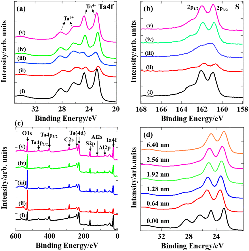 | ||
| Fig. 7 XPS spectra of the selected elements (a) tantalum (b) and sulphur, and (c) wide scan XPS spectra. Ta5+ shows surface oxidation due to air exposure. No chlorine was detected, meaning the complete decomposition of TaCl5. (d) Depth profile of sample (iv) with unidirectional triangle domains for Ta 4f. The thickness of the native oxide was less than 2.56 nm. | ||
In order to investigate the growth mechanism, the surface morphology of sample (iv) with unidirectional domains was observed by SEM and AFM as shown in Fig. S9(a) and S10(a).† Furthermore, the average thickness was determined to be 154 nm by AFM as shown in Fig. S10(b),† and the vertical growth rate was calculated to be 0.51 nm s−1 (nearly one layer per second). Since such fast growth restricts obtaining few-layer TaS2 films, hydrogen concentration (partial pressure) should be appropriately adjusted to control the growth kinetics in the near future. The possibility of the Frank–van der Merwe mode (layer-by-layer growth)58 can be easily eliminated by observing the characteristic triangular domains (see also the OM images in Fig. 3) with the relative thickness. An EDS analysis and Raman mapping shown in Fig. S9(b) and S11† revealed that TaS2 was not grown in the region where triangular domains were absent, while TaS2 was detected at the triangle domain. Additionally, the ratio of Ta and S was determined to be 1![[thin space (1/6-em)]](https://www.rsc.org/images/entities/char_2009.gif) :2.26, which means a slightly sulphur-rich composition. This elemental analysis and Raman mapping led us to the Volmer–Weber mode (island growth), not the Stranski–Krastanov mode (layer and island growth).59 Note that no chlorine impurities were detected by the EDS analysis, consistent with the XPS spectra. To further gain insight into the growth mechanism, we closely observed the surface of a triangular domain as shown in Fig. 8(a) and (b). The layered structure was seen at the edge of the triangular domain, which reflects the crystal structure of TaS2. Furthermore, a triangular pyramidal protrusion, previously observed in the growth of NbS2 films,15 was found in Fig. 8(a) with a considerable height, indicating that the nucleation and lateral growth occurred on the surface of the triangle flakes. The flatness of the triangle domain surface was probed by AFM as shown in Fig. 8(c). Intriguingly, the step-and-terrace structure was observed at the top surface even though it was oxidized by air, illustrating the high crystal quality. Fig. 8(d) shows the step heights measured at three selected lines. The average step height (0.99 nm) was greater than the thickness of a single layer of TaS2 (0.60 nm) due to the surface oxidation. The absence of spiral defects also supported the high crystal quality of the grown TaS2 flakes.
:2.26, which means a slightly sulphur-rich composition. This elemental analysis and Raman mapping led us to the Volmer–Weber mode (island growth), not the Stranski–Krastanov mode (layer and island growth).59 Note that no chlorine impurities were detected by the EDS analysis, consistent with the XPS spectra. To further gain insight into the growth mechanism, we closely observed the surface of a triangular domain as shown in Fig. 8(a) and (b). The layered structure was seen at the edge of the triangular domain, which reflects the crystal structure of TaS2. Furthermore, a triangular pyramidal protrusion, previously observed in the growth of NbS2 films,15 was found in Fig. 8(a) with a considerable height, indicating that the nucleation and lateral growth occurred on the surface of the triangle flakes. The flatness of the triangle domain surface was probed by AFM as shown in Fig. 8(c). Intriguingly, the step-and-terrace structure was observed at the top surface even though it was oxidized by air, illustrating the high crystal quality. Fig. 8(d) shows the step heights measured at three selected lines. The average step height (0.99 nm) was greater than the thickness of a single layer of TaS2 (0.60 nm) due to the surface oxidation. The absence of spiral defects also supported the high crystal quality of the grown TaS2 flakes.
 | ||
| Fig. 8 (a) SEM image of the TaS2 triangle domain. This is a magnified area of the rectangle shown in Fig. S9(a).† (b) AFM image of the TaS2 triangle domain. (c) Step-and-terrace structure on the surface of the TaS2 triangle domain shown in Fig. 8(b). (d) Step height profiles at lines (I)–(III) in (c). The average step height was calculated to be 0.99 nm. | ||
4 Conclusions
The epitaxial growth of unidirectional TaS2 triangular flakes on c-plane sapphire using an APCVD with a separate-flow and program-controlled system was demonstrated. It was critical to precisely control the growth conditions (precursor concentration, gas flow rate, temperature) and supply sequence for obtaining the unidirectional epitaxial films with high crystal quality. The sample position was also essential and should be placed at the same location to remove the effects of the temperature gradient and convection, which was clarified by CFD simulations. The growth mechanism was determined to be the Volmer–Weber mode without spiral defects; nucleation and lateral growth took place on the surface of the existing TaS2 triangular flakes. It is expected that our separate-flow APCVD opens up a new way to synthesize TMDCs with various transition metals including alloys since most chloride precursors show high volatility below 200 °C.Author contributions
The manuscript was written through the contributions of all authors. All authors have given approval to the final version of the manuscript.Conflicts of interest
There are no conflicts to declare.Acknowledgements
This research was supported by the Japan Society for the Promotion of Science (JSPS) KAKENHI Grant Number 22K04881 and the Toyota Physical and Chemical Research Institute. We greatly thank Dr. Hiroki Konno at Toho University for letting us use the XRD.References
- J. Gao, J. W. Park, K. Kim, S. K. Song, H. R. Park, J. Lee, J. Park, F. Chen, X. Luo, Y. Sun and H. W. Yeom, Nano Lett., 2020, 20, 6299–6305 CrossRef CAS PubMed.
- J. Pandey and A. Soni, Phys. Rev. Res., 2020, 2, 33118 CrossRef CAS.
- H. Bretscher, Z. Li, J. Xiao, D. Y. Qiu, S. Refaely-Abramson, J. A. Alexander-Webber, A. Tanoh, Y. Fan, G. Delport, C. A. Williams, S. D. Stranks, S. Hofmann, J. B. Neaton, S. G. Louie and A. Rao, ACS Nano, 2021, 15, 8780–8789 CrossRef CAS PubMed.
- H. Suzuki, R. Hashimoto, M. Misawa, Y. Liu, M. Kishibuchi, K. Ishimura, K. Tsuruta, Y. Miyata and Y. Hayashi, ACS Nano, 2022, 16, 11360–11373 CrossRef CAS PubMed.
- T. Li, W. Guo, L. Ma, W. Li, Z. Yu, Z. Han, S. Gao, L. Liu, D. Fan, Z. Wang, Y. Yang, W. Lin, Z. Luo, X. Chen, N. Dai, X. Tu, D. Pan, Y. Yao, P. Wang, Y. Nie, J. Wang, Y. Shi and X. Wang, Nat. Nanotechnol., 2021, 16, 1201–1207 CrossRef CAS PubMed.
- M. Chubarov, T. H. Choudhury, D. R. Hickey, S. Bachu, T. Zhang, A. Sebastian, A. Bansal, H. Zhu, N. Trainor, S. Das, M. Terrones, N. Alem and J. M. Redwing, ACS Nano, 2021, 15, 2532–2541 CrossRef CAS PubMed.
- T. Yanase, F. Uehara, I. Naito, T. Nagahama and T. Shimada, ACS Appl. Nano Mater., 2020, 3, 10462–10469 CrossRef CAS.
- H. J. Choi, Y. S. Jung, S. M. Lee, S. Kang, D. Seo, H. Kim, H. Choi, G. Lee and Y. S. Cho, Cryst. Growth Des., 2020, 20, 2698–2705 CrossRef CAS.
- P. Yang, S. Zhang, S. Pan, B. Tang, Y. Liang, X. Zhao, Z. Zhang, J. Shi, Y. Huan, Y. Shi, S. J. Pennycook, Z. Ren, G. Zhang, Q. Chen, X. Zou, Z. Liu and Y. Zhang, ACS Nano, 2020, 14, 5036–5045 CrossRef CAS PubMed.
- W. Wang, H. Shu, J. Wang, Y. Cheng, P. Liang and X. Chen, ACS Appl. Mater. Interfaces, 2020, 12, 9563–9571 CrossRef CAS PubMed.
- D. Zhou, H. Shu, C. Hu, L. Jiang, P. Liang and X. Chen, Cryst. Growth Des., 2018, 18, 1012–1019 CrossRef CAS.
- J. Chen, X. Zhao, S. J. R. Tan, H. Xu, B. Wu, B. Liu, D. Fu, W. Fu, D. Geng, Y. Liu, W. Liu, W. Tang, L. Li, W. Zhou, T. C. Sum and K. P. Loh, J. Am. Chem. Soc., 2017, 139, 1073–1076 CrossRef CAS PubMed.
- H. Yu, M. Liao, W. Zhao, G. Liu, X. J. Zhou, Z. Wei, X. Xu, K. Liu, Z. Hu, K. Deng, S. Zhou, J. A. Shi, L. Gu, C. Shen, T. Zhang, L. Du, L. Xie, J. Zhu, W. Chen, R. Yang, D. Shi and G. Zhang, ACS Nano, 2017, 11, 12001–12007 CrossRef CAS PubMed.
- X. Pan, T. Yang, H. Bai, J. Peng, L. Li, F. Jing and H. Qiu, Nanomaterials, 2023, 13, 1806 CrossRef CAS PubMed.
- T. Yanase, S. Watanabe, M. Weng, M. Wakeshima, Y. Hinatsu, T. Nagahama and T. Shimada, Cryst. Growth Des., 2016, 16, 4467–4472 CrossRef CAS.
- X. Wang, H. Liu, J. Wu, J. Lin, W. He, H. Wang, X. Shi, K. Suenaga and L. Xie, Adv. Mater., 2018, 30, 1–7 Search PubMed.
- M. Leem, H. Lee, T. Park, W. Ahn, H. Kim, E. Lee and H. Kim, Appl. Surf. Sci., 2020, 509, 144701 CrossRef CAS.
- Q. Ji, M. Kan, Y. Zhang, Y. Guo, D. Ma, J. Shi, Q. Sun, Q. Chen, Y. Zhang and Z. Liu, Nano Lett., 2015, 15, 198–205 CrossRef CAS PubMed.
- L. Tang, T. Li, Y. Luo, S. Feng, Z. Cai, H. Zhang, B. Liu and H. M. Cheng, ACS Nano, 2020, 14, 4646–4653 CrossRef CAS PubMed.
- W. Chen, J. Zhao, J. Zhang, L. Gu, Z. Yang, X. Li, H. Yu, X. Zhu, R. Yang, D. Shi, X. Lin, J. Guo, X. Bai and G. Zhang, J. Am. Chem. Soc., 2015, 137, 15632–15635 CrossRef CAS PubMed.
- Q. Wang, N. Li, J. Tang, J. Zhu, Q. Zhang, Q. Jia, Y. Lu, Z. Wei, H. Yu, Y. Zhao, Y. Guo, L. Gu, G. Sun, W. Yang, R. Yang, D. Shi and G. Zhang, Nano Lett., 2020, 20, 7139–7199 Search PubMed.
- J. Zhou, J. Lin, X. Huang, Y. Zhou, Y. Chen, J. Xia, H. Wang, Y. Xie, H. Yu, J. Lei, D. Wu, F. Liu, Q. Fu, Q. Zeng, C. H. Hsu, C. Yang, L. Lu, T. Yu, Z. Shen, H. Lin, B. I. Yakobson, Q. Liu, K. Suenaga, G. Liu and Z. Liu, Nature, 2018, 556, 355–359 CrossRef CAS PubMed.
- S. Li, Y. C. Lin, W. Zhao, J. Wu, Z. Wang, Z. Hu, Y. Shen, D. M. Tang, J. Wang, Q. Zhang, H. Zhu, L. Chu, W. Zhao, C. Liu, Z. Sun, T. Taniguchi, M. Osada, W. Chen, Q. H. Xu, A. T. S. Wee, K. Suenaga, F. Ding and G. Eda, Nat. Mater., 2018, 17, 535–542 CrossRef CAS PubMed.
- M. Li, J. Yao, X. Wu, S. Zhang, B. Xing, X. Niu, X. Yan, Y. Yu, Y. Liu and Y. Wang, ACS Appl. Mater. Interfaces, 2020, 12, 6276–6282 CrossRef CAS PubMed.
- B. Kalanyan, W. A. Kimes, R. Beams, S. J. Stranick, E. Garratt, I. Kalish, A. V. Davydov, R. K. Kanjolia and J. E. Maslar, Chem. Mater., 2017, 29, 6279–6288 CrossRef CAS PubMed.
- P. K. Sahoo, S. Memaran, Y. Xin, L. Balicas and H. R. Gutiérrez, Nature, 2018, 553, 63–67 CrossRef CAS PubMed.
- P. K. Sahoo, S. Memaran, F. A. Nugera, Y. Xin, T. D. Marquez, Z. Lu, W. Zheng, N. D. Zhigadlo, D. Smirnov, L. Balicas and H. R. Gutiérrez, ACS Nano, 2019, 13, 12372–12384 CrossRef CAS PubMed.
- S. Berweger, H. Zhang, P. K. Sahoo, B. M. Kupp, L. Blackburn, E. M. Miller, T. M. Wallis, D. V. Voronine, P. Kabos and S. U. Nanayakkara, ACS Nano, 2020, 14, 14080–14090 CrossRef CAS PubMed.
- F. A. Nugera, P. K. Sahoo, Y. Xin, S. Ambardar, D. V. Voronine, U. J. Kim, Y. Han, H. Son and H. R. Gutiérrez, Small, 2022, 18, 2106600 CrossRef CAS PubMed.
- T. Shimada, F. S. Ohuchi and A. Koma, Surf. Sci., 1993, 291, 57–66 CrossRef CAS.
- L. F. Mattheiss, Phys. Rev. B: Solid State, 1973, 8, 3719–3740 CrossRef CAS.
- X. Zhao, P. Song, C. Wang, A. C. Riis-Jensen, W. Fu, Y. Deng, D. Wan, L. Kang, S. Ning, J. Dan, T. Venkatesan, Z. Liu, W. Zhou, K. S. Thygesen, X. Luo, S. J. Pennycook and K. P. Loh, Nature, 2020, 581, 171–177 CrossRef CAS PubMed.
- Z. Lin, T. Lin, T. Lin, X. Tang, G. Chen, J. Xiao, H. Wang, W. Wang and G. Li, Appl. Phys. Lett., 2023, 122, 131101 CrossRef CAS.
- W. Song, J. Chen, Z. Li and X. Fang, Adv. Mater., 2021, 33, 2101059 CrossRef CAS PubMed.
- W. Wang, H. Jiang and L. Li, Rep. Prog. Phys., 2021, 84, 086501 CrossRef CAS PubMed.
- Z. Zou, J. Liang, X. Zhang, C. Ma, P. Xu, X. Yang, Z. Zeng, X. Sun, C. Zhu, D. Liang, X. Zhuang, D. Li and A. Pan, ACS Nano, 2021, 15, 10039–10047 CrossRef CAS PubMed.
- T. Yanase, S. Watanabe, M. Weng, T. Nagahama and T. Shimada, J. Nanosci. Nanotechnol., 2016, 16, 3223–3227 CrossRef CAS PubMed.
- Y. Huan, J. Shi, X. Zou, Y. Gong, C. Xie, Z. Yang, Z. Zhang, Y. Gao, Y. Shi, M. Li, P. Yang, S. Jiang, M. Hong, L. Gu, Q. Zhang, X. Yan and Y. Zhang, J. Am. Chem. Soc., 2019, 141, 18694–18703 CrossRef CAS PubMed.
- R. Zhao, B. Grisafe, R. K. Ghosh, K. Wang, S. Datta and J. Robinson, Nanoscale, 2019, 11, 6016–6022 RSC.
- Q. Yu, Y. Luo, S. Qiu, Q. Li, Z. Cai, Z. Zhang, J. Liu, C. Sun and B. Liu, ACS Nano, 2019, 13, 11874–11881 CrossRef CAS PubMed.
- M. Mattinen, G. Popov, M. Vehkamäki, P. J. King, K. Mizohata, P. Jalkanen, J. Räisänen, M. Leskelä and M. Ritala, Chem. Mater., 2019, 31, 5713–5724 CrossRef CAS.
- I. I. Barin, Thermochemical Data of Pure Substances, Wiley-VCH, Weinheim, 1995 Search PubMed.
- J. Dong, L. Zhang, X. Dai and F. Ding, Nat. Commun., 2020, 11, 5862 CrossRef CAS PubMed.
- D. Dumcenco, D. Ovchinnikov, K. Marinov, P. Lazić, M. Gibertini, N. Marzari, O. L. Sanchez, Y. C. Kung, D. Krasnozhon, M. W. Chen, S. Bertolazzi, P. Gillet, A. F. I. Morral, A. Radenovic and A. Kis, ACS Nano, 2015, 9, 4611–4620 CrossRef CAS PubMed.
- A. Spijkerman, J. L. de Boer, A. Meetsma, G. A. Wiegers and S. van Smaalen, Phys. Rev. B: Condens. Matter Mater. Phys., 1997, 56, 13757–13767 CrossRef CAS.
- Y. Tison, H. Martinez, I. Baraille, M. Loudet and D. Gonbeau, Surf. Sci., 2004, 563, 83–98 CrossRef CAS.
- Y. Feng, S. Gong, E. Du, X. Chen, R. Qi, K. Yu and Z. Zhu, J. Phys. Chem. C, 2018, 122, 2382–2390 CrossRef CAS.
- E. Kovalska, P. K. Roy, N. Antonatos, V. Mazanek, M. Vesely, B. Wu and Z. Sofer, npj 2D Mater. Appl., 2021, 5, 1–9 CrossRef.
- J. Martincová, M. Otyepka and P. Lazar, ChemPlusChem, 2020, 85, 2557–2564 CrossRef PubMed.
- J. Luxa, V. Mazánek, M. Pumera, P. Lazar, D. Sedmidubský, M. Callisti, T. Polcar and Z. Sofer, Chem. – Eur. J., 2017, 23, 8082–8091 CrossRef CAS PubMed.
- A. W. Tsen, R. Hovden, D. Wang, Y. D. Kim, K. A. Spoth, Y. Liu, W. Lu, Y. Sun, J. C. Hone, L. F. Kourkoutis, P. Kim and A. N. Pasupathy, Proc. Natl. Acad. Sci. U. S. A., 2015, 112, 15054–15059 CrossRef CAS PubMed.
- S. L. L. M. Ramos, R. Plumadore, J. Boddison-Chouinard, S. W. Hla, J. R. Guest, D. J. Gosztola, M. A. Pimenta and A. Luican-Mayer, Phys. Rev. B, 2019, 100, 165414 CrossRef CAS.
- R. Albertini, R. Zhao, R. L. McCann, S. Feng, M. Terrones, J. K. Freericks, J. A. Robinson and A. Y. Liu, Phys. Rev. B, 2016, 93, 1–7 CrossRef.
- J. A. Holy, K. C. Woo, M. V. Klein and F. C. Brown, Phys. Rev. B: Solid State, 1977, 16, 3628–3637 CrossRef CAS.
- J. Peng, J. Wu, X. Li, Y. Zhou, Z. Yu, Y. Guo, J. Wu, Y. Lin, Z. Li, X. Wu, C. Wu and Y. Xie, J. Am. Chem. Soc., 2017, 139, 9019–9025 CrossRef CAS PubMed.
- J. Ribeiro-Soares, R. M. Almeida, E. B. Barros, P. T. Araujo, M. S. Dresselhaus, L. G. Cançado and A. Jorio, Phys. Rev. B: Condens. Matter Mater. Phys., 2014, 90, 115438 CrossRef.
- M. Zhang, Y. He, D. Yan, H. Xu, A. Wang, Z. Chen, S. Wang, H. Luo and K. Yan, Nanoscale, 2019, 11, 22255–22260 RSC.
- H. Heo, J. H. Sung, J. H. Ahn, F. Ghahari, T. Taniguchi, K. Watanabe, P. Kim and M. H. Jo, Adv. Electron. Mater., 2017, 3, 1–7 Search PubMed.
- H. Q. Ta, D. J. Perello, D. L. Duong, G. H. Han, S. Gorantla, V. L. Nguyen, A. Bachmatiuk, S. V. Rotkin, Y. H. Lee and M. H. Rümmeli, Nano Lett., 2016, 16, 6403–6410 CrossRef CAS PubMed.
Footnote |
| † Electronic supplementary information (ESI) available. See DOI: https://doi.org/10.1039/d3ce00906h |
| This journal is © The Royal Society of Chemistry 2024 |