
Directional lateral crystallization of vacuum-deposited C8-BTBT thin films via liquid crystal phase by a seeded horizontal temperature gradient cooling technique†
Kanae
Tsujita
a,
Shingo
Maruyama
 *a,
Yosesi
Shibata
b,
Tomoyuki
Koganezawa
c,
Kenichi
Kaminaga
a,
Hideo
Fujikake
b and
Yuji
Matsumoto
a
*a,
Yosesi
Shibata
b,
Tomoyuki
Koganezawa
c,
Kenichi
Kaminaga
a,
Hideo
Fujikake
b and
Yuji
Matsumoto
a
aDepartment of Applied Chemistry, Graduate School of Engineering, Tohoku University, Sendai, Miyagi 980-8579, Japan. E-mail: maruyama-s@tohoku.ac.jp
bDepartment of Electronic Engineering, Graduate School of Engineering, Tohoku University, Sendai, Miyagi 980-8579, Japan
cJapan Synchrotron Radiation Research Institute (JASRI), Sayo, Hyogo 679-5198, Japan
First published on 1st November 2022
Abstract
We have demonstrated the directional lateral crystallization of thin film C8-BTBT which is pre-vacuum-deposited on a SiO2/Si substrate, with good controllability of the crystallization rate, by cooling from its liquid crystal state with a constant horizontal temperature gradient using a custom-made substrate holder. From in situ polarized optical microscope observation of the crystallization process in detail, it was revealed that the lateral crystal growth proceeds via liquid crystal phase from the lower-temperature side with seed crystals to the neighboring higher temperature side with small supercooling between them as a driving force. Moreover, the propagation rate of crystallization could be intentionally controlled by changing the cooling rate of and the degree of temperature gradient over the substrate, realizing large single crystal domains under the optimized conditions. The orientation analysis of the obtained C8-BTBT thin films with large single-crystal domains was carried out by means of grazing incidence X-ray diffraction and their field effect transistor performance was discussed as well.
1. Introduction
Controlling the grain/domain growth in crystalline organic semiconductor (OSC) thin films is important for high-performance organic electronic devices because the grain/domain boundary typically hampers carrier transport.1–4 Hence, research and development of a fabrication process to obtain single crystalline thin films with higher quality have been intensively made for the last few decades. In the state-of-the-art solution processes, high-quality single crystalline organic thin films have been realized by using various techniques such as zone casting,5,6 solution shearing,7 edge-casting,8 ink-jet printing,9 dip coating,10 off-centre spin-coating,11 blade coating,12,13 bar coating,14 and water surface drag coating.15 A key feature shared by these techniques is how to control the directional growth: the evaporation and/or flow of a solution containing OSC molecules over a substrate determines the nucleation point and direction of crystal growth, which often results in the ordered in-plane molecular orientation. On the other hand, a vacuum deposition technique for the growth of organic thin films has advantages over the solution processes in thickness controllability and easy preparation of complex stacked structures. However, the obtained organic thin films inevitably include small grains/domains with their sizes of around several micrometres. To make the matter worse, when grown on non-single crystal substrates, such as SiO2/Si, the films show random in-plane orientations because the nucleation and growth of crystals are dominated by random nucleation and micrometre scale surface molecular diffusion though they can be to some extent controlled by the deposition rate and the substrate temperature.16One simple way to promote the directional crystal growth in a vacuum-deposited thin film is to carry out a post-annealing with a lateral temperature gradient. Temperature gradient crystallization is a method widely used for the directional crystal growth, as represented by the well-known Bridgman method.17,18 In this method, during crystal growth in a furnace a crucible is moved in accordance with the crystal growth rate along the direction of a temperature gradient. Recently, Schweicher et al. and their group applied this methodology not only to non-semiconducting organic materials19–21 but also to OSC materials: 20–50 μm-thick film of 2,2′:5′,2-terthiophene (3T)22 and 2–3 μm-thick films of the blend of 2,7-didodecyl[1]benzothieno[3,2-b][1]benzothiophene (C8-BTBT) and tetracyanoquinodimethane (TCNQ)23 were prepared from the melt of powder in a glass-sandwiched cell, while a <100 nm-thick C8-BTBT thin film was also prepared by spin-coating on a glass substrate.24 In their apparatus, the sample is moved from to one hot zone (stage) to the other cold zone (stage) at a constant rate, which process is similar to the horizontal Bridgman method. Fujieda et al. reported a temperature gradient solidification of spin-coated C8-BTBT thin films in air, where the temperature gradient was created by various methods. One is attaching one corner of a substrate to a hot stage so that the substrate is hung with the other corner exposed to the air.25 The other is putting a substrate on an aluminium plate bridging two heat stages and irradiating a halogen light at a selected area of the substrate, under cooling either of the heat stages.26 Kim et al. demonstrated the growth of N,N′-bis(2-ethylhexyl)-1,7-dicyanoperylene-3,4:9,10-bis(dicarboxyimide) (PDI–CN2) thin films on substrates with temperature gradient during the vacuum deposition, in which process the temperature gradient was made by vertically tilting the substrate so that its one edge alone contacts with a heating plate with vertically tilting the substrate.27 Stimulated by these advanced reports, here, we propose a new type of sample stage and procedure suitable for vacuum process in order to carry out the temperature gradient crystallization of OSC thin films. When an oblong substrate is mounted on the sample stage, two of its edges opposite to each other along the oblong direction are directly attached to and fixed on the hot and cold stages, respectively, under the control of their temperatures independently, achieving precision control of temperature gradient.
To demonstrate temperature gradient crystallization in vapor-deposited thin films, we choose C8-BTBT28 as a model material of thin film OSC. Since C8-BTBT can be deposited by vacuum deposition29 and it shows a smectic A (SmA) liquid crystal phase at 110–125 °C,30 cooling crystallization via the SmA phase is available to the vacuum-deposited thin films.24–26 Moreover, the 2-dimensional layering nature and wetting behaviour of C8-BTBT at the SmA phase on a SiO2/Si substrate30 ensure the thin film form to be stabilized during the annealing without 3-dimensional droplet formation.24 It should be noted that we recently demonstrated the fabrication of high-quality vacuum-deposited thin films of an ionic liquid crystal by the crystallization from its SmA phase on SiO2/Si substrates.31
In addition to the temperature gradient, which mainly determines the direction of crystal growth, the control of nucleation is another important issue in crystal growth, because it often governs the crystal orientation, and because the domain size is related to the balance between the rates of nucleation and growth. To control the nucleation, seed crystals have often been used. The crystal seeds in a thin film can be formed by various methods such as contact freezing,32–34 producing bespoke microstructures by manipulating thin-film topography,35 and self-seeding.22 In this study, we prepared a seed crystal region in C8-BTBT thin films by making the low-temperature side of a substrate below the crystal-SmA transition temperature (110 °C) and discussed their growth behaviour and orientation as compared with the case without seeding.
2. Experimental
2.1 Materials
C8-BTBT was purchased from Sigma-Aldrich and used without further purification. For a substrate, a heavily doped n-type Si(001) wafer with 200 nm-thick thermally grown oxide layer was used after cutting it to a size of 5–10 mm × 20 mm. The substrate was sequentially cleaned by sonication in acetone and ethanol for 5 min each in two sets, and then treated with UV ozone for 20 min.2.2 Thin film fabrication and post-annealing
Fig. 1 shows a schematic illustration of a vacuum deposition chamber for thin film fabrication and post-annealing with a custom-made substrate holder. The base pressure of this chamber was ∼10−6 Torr. A substrate was directly mounted on a custom-made substrate holder equipped with two independently temperature-controlled heating stages. A substrate was clamped on the aluminum stage with a small amount of high-vacuum grease (Dow Corning Toray) used to ensure the thermal contact between the substrate and the heating stages. The temperatures of the aluminum stages are monitored by the thermocouples (TC1 and TC2) and controlled independently by ceramic heaters. The heater 1 is attached to the cooling block, in which liquid nitrogen (LN2) can be flowed, so that a large temperature gradient over 100 °C in a substrate can be made. The distance between the two stages where the thermal gradient will be generated is 11 mm. This substrate holder enables us to carry out during- or post-deposition process without moving the sample, which is different from the system in which the sample is displaced between different temperature zones, presented in literature.22–24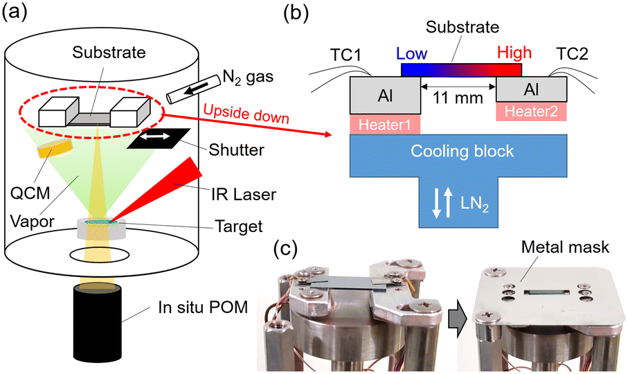 | ||
| Fig. 1 (a) Schematic of the deposition chamber equipped with a temperature gradient substrate holder and a in situ polarized optical microscope (POM). (b) Schematic illustration and (c) photograph of a custom-made temperature gradient substrate holder. | ||
100 nm C8-BTBT thin films were deposited on the substrates at room temperature with the deposition rate of 7 nm min−1 by a continuous wave infrared (CW-IR) laser evaporation technique.36,37 The deposition of thin films for temperature gradient post-annealing was conducted through a metal mask, which covers the edges of a substrate to prevent edge effects (e.g. substrate edge often becomes a nucleation center) in the crystallization process. The thickness and deposition rate were monitored by quartz crystal microbalance (QCM) during the deposition. Temperature gradient post-annealing was conducted for the as-deposited C8-BTBT thin film in a nitrogen atmosphere (200 Torr) to prevent re-evaporation of the thin film at high-temperature (see details in Fig. S1†). Temperatures of the two stages were increased with the rate of 10 °C min−1 and kept 1 min after reaching to the target temperatures, and then the two stages were cooled down with the rates of 0.03–16.5 °C min−1.
2.3 In situ crystal growth observation
In situ polarized optical microscope (POM) observation of crystal growth in the thin films was carried out by using a long focal length microscope (a focal length of 85 mm, KEYENCE VH-Z50W) set under the bottom view port (Fig. 1). The observation was done in reflection mode with crossed polarizers.2.4 Ex situ thin film characterizations
Ex situ POM observation was carried out using ECLIPSCE LV100ND (Nikon) in reflection mode with crossed-polarizers. Surface morphology of the thin films was observed by atomic force microscopy (AFM) using a SPI3800N/SPA-400 scanning probe microscope (SII NanoTechnology) in a tapping mode.Out-of-plane X-ray diffraction (XRD) measurement was performed by a Bruker D8 diffractometer with a Lynxeye detector using Cu Kα radiation. In-plane crystallographic orientation of the film was obtained by grazing incidence X-ray diffraction (GIXD) performed at SPring-8 BL19B2 beamline using synchrotron X-ray beam (energy of 12.4 keV, beam height of 0.2 mm and beam width of 1 mm). The incident angle was set to 0.12°, which is lower than the critical angle of SiO2. Diffraction patterns were recorded by a 2D area detector (Pilatus 300 K, Dectris), which was set to the position with the camera length of 173.7 mm, with rotating the sample 360° around the surface normal (rotation in φ angle) and then converted into an in-plane reciprocal space map at qz ≈ 0.38
2.5 Organic field effect transistor (OFET) fabrication
Bottom-gate top-contact organic field effect transistors (OFET) were fabricated on a SiO2(200 nm)/Si single substrate. Au source and drain electrodes were thermally deposited via a metal mask with channel lengths (L) of 50, 75, 100, and 125 μm and a width (W) of 1 mm. Electrical measurements were carried out in air using a source measure unit (Keysight B2902A). The field effect mobility in the saturation region of the device was determined from the following equation:where Ci, ID and VG are the capacitance of SiO2 insulating layer (measured value of 1.529 × 10⁻⁸ F cm−2 was used), drain current and gate voltage, respectively.
3. Results and discussion
3.1 Effect of post-annealing temperature
We firstly investigated the morphology of C8-BTBT thin films as a function of post-annealing temperatures. Fig. 2(a) shows stitched ex situ POM images taken over the entire temperature gradient region of the sample, which was post-annealed with a temperature gradient of 30 to 140 °C and cooled down at 1 °C min−1. In the regions annealed at the temperature range for the crystal phase of C8-BTBT (below 110 °C), small grains with a size of less than a few tens micrometres were found. On the other hand, the region annealed at the SmA phase of C8-BTBT (110 to 125 °C) showed quite large grains with a size of more than a millimetre scale. At the designed temperatures above 140 °C, the formation of many droplets was observed, which is due to the dewetting of the thin film at the isotropic liquid phase. This temperature of 140 °C is higher than the bulk SmA-isotropic transition temperature (125 °C), which might be due to that the temperature gradient was not linear near the aluminium stages as the designed temperature. Fig. 2(b) shows AFM images taken at the region where the thin film was post-annealed at the crystal phase (the position #1 and 2 in Fig. 2(a)) and at the SmA phase (position #3 in Fig. 2(a)). While molecular steps with a height of 2.7–2.9 nm were observed for all these images, the size of terraces became larger with the post-annealing temperature, resulting in the decrease of the root-mean-squared (RMS) roughness, especially for the post-annealing at the SmA phase. Similar morphological improvement in liquid crystalline materials by the post-annealing at liquid crystal temperature has been reported in our previous study.31Fig. 2(c) shows out-of-plane XRD patterns taken at around positions #1–3 in Fig. 2(a). All the patterns showed 00l diffraction peaks indicating (001)-oriented C8-BTBT thin films are grown. Moreover, there was no significant difference in the layer spacing with the layer spacing of 2.91 nm,29 indicating the negligible change of the layering structure by the post-annealing, in contrast to the large morphological change.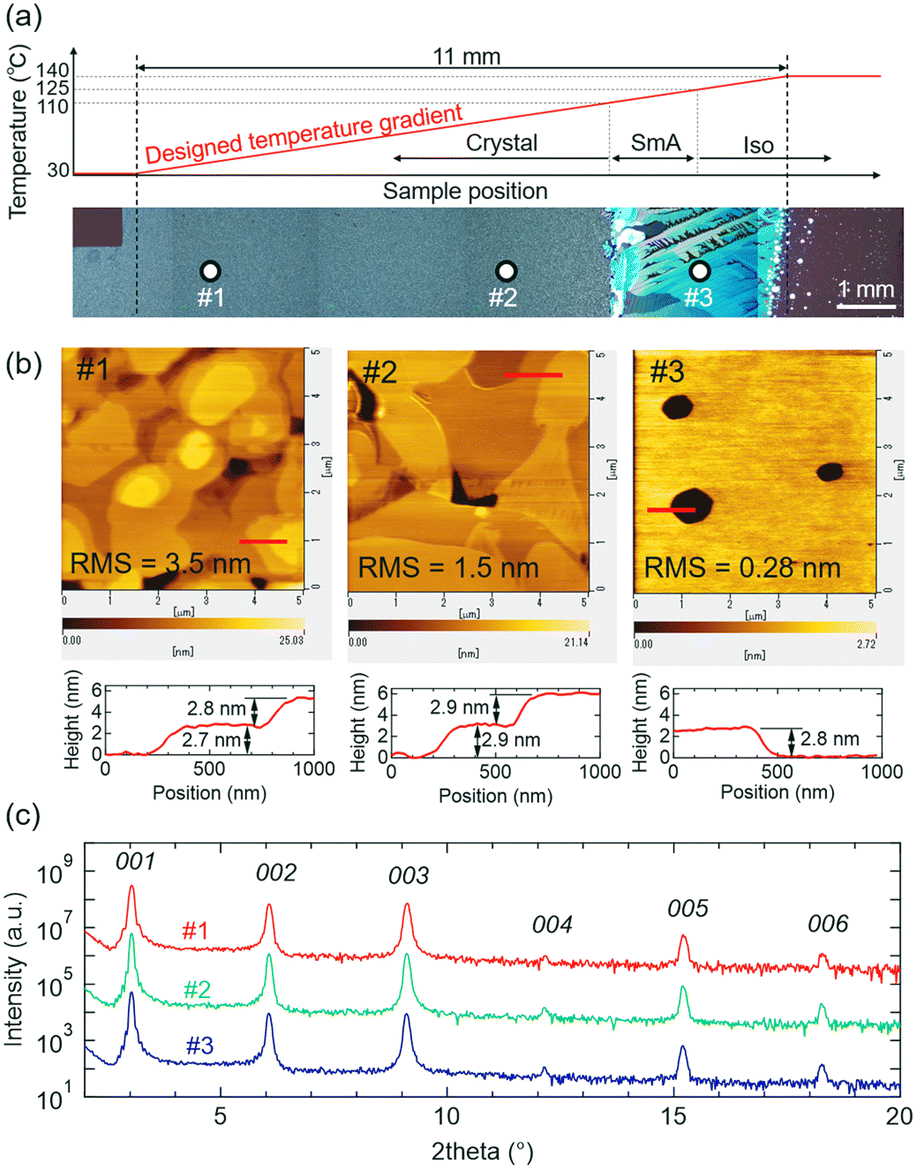 | ||
| Fig. 2 (a) Stitched ex situ POM images of C8-BTBT thin film after the post-annealing with a temperature gradient from 30 to 140 °C. Designed temperature gradient along the sample position and bulk phases are also shown (top). (b) AFM images (5 μm × 5 μm) with corresponding line profiles taken at the positions #1–3 denoted in (a). (c) Out-of-plane XRD patterns taken at around the positions #1–3. | ||
3.2 Control of crystallization direction by temperature gradient
Next, we apply the temperature gradient technique to the C8-BTBT thin film growth. As-deposited C8-BTBT thin films were post-annealed and crystalized by cooling both sides of the substrate at 1 °C min−1 from the following three different conditions: a uniform temperature of 120 °C (Fig. 3(a)), temperature-gradient of 110–120 °C (Fig. 3(c)), and temperature gradient of 107–117 °C (Fig. 3(e)). Just before the cooling step starts, the entire thin films become SmA phase under the first two conditions, while at the low-temperature side under the last condition the crystal phase remains, which works as seed crystals. Fig. 3(b), (d), and (f) show in situ POM images of the crystallization process of C8-BTBT thin films for those three conditions, namely uniform temperature, gradient temperature without seeding, and gradient temperature with seeding, respectively (see also Videos S1–S3, ESI†). In the case of uniform temperature, the visible nucleation occurred spontaneously at ∼97 °C (Fig. 3(b)), which is far below the SmA-Crystal transition temperature (110 °C) and indicates a large supercooling (ΔT ≈ 13 °C). The observed nucleation point is located at ∼3.2 mm away from the left aluminium stage, which can be due to that the temperature near the center of the substrate was slightly lower than the area attached to the aluminium stage by the thermal radiation. The crystal grew radially as indicated by the white arrows with the growth rate (Vcr) of ∼880 μm s−1. In the case of the temperature gradient growth without seeding (Fig. 3(d)), the visible nucleation was occurred at the low-temperature region at ∼95 °C with a large supercooling (ΔT ≈ 15 °C) and the thin film was crystallized from the nucleation point radially toward the high-temperature side at the Vcr of ∼780 μm s−1. These crystallization behaviours (nucleation temperature and growth rate) are similar to the crystal growth at uniform temperature (Fig. 3(b)), except that the nucleation point is controlled to the lower temperature region. On the other hand, in the case of the temperature gradient growth with seeding (Fig. 3(f)), the crystal growth started from the edge of the seed crystals with small supercooling (ΔT ≈ 3 °C). The crystal growth begins with a large number of seed crystals, but as growth proceeds, only a few crystals, which have fast growth directions almost parallel to the direction of the temperature gradient (indicated by the white arrows), are finally selected to survive, which is known as geometrical selection.39 The Vcr of these crystals was estimated to be ∼39 μm s−1, which is close to the designed propagation rate of crystallization (in our cases, this is equals to the crystal growth rate) calculated from the temperature gradient and cooling rate. We will discuss the details of the relationship between the growth rate and cooling rate in the next section.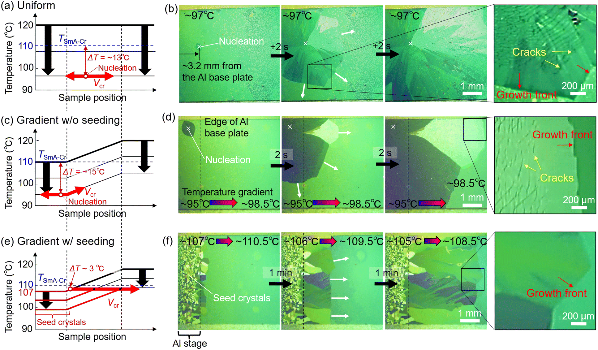 | ||
| Fig. 3 Schematic illustration of the temperature distributions in the samples (a–c) and in situ POM observations (b–f) for the samples (a and b) cooling from a uniform temperature of 120 °C, (c and d) 110–120 °C temperature-gradient, and (e and f) 107–117 °C temperature gradient. | ||
Next, ex situ polarized optical microscope images for these three samples are shown in Fig. 4. Many cracks were observed in all the samples which would be due to the large difference in cooling shrinkage between the thin film and substrate. When the entire thin film is annealed up to the temperature of the SmA phase, the cracks are formed running along the direction almost perpendicular (though distorted) to the direction of crystallization as seen in Fig. 4(a) and (b). On the other hand, when the crystallization was carried out with temperature gradient with seeding, the cracks were not aligned in the direction of crystal growth but aligned more straight in each domain than the case without seeding (Fig. 4(c)). This trend is also observed in microscopic AFM observation as shown in Fig. S2.† From the in situ observations, the formation of the cracks was occurred just after the crystallization for the case of uniform temperature and gradient without seeding, but interestingly, the position of cracking can be observed at 300–400 μm away from the growth front (right end magnified images in Fig. 3(b) and (d), see also Videos S1 and S2†). In contrast, in the case of temperature gradient growth with seeding, there are no cracks near the growth front as seen in Fig. 3(f), and the cracking was started at ∼96 °C from the low-temperature side (see Video S3, ESI†). This result suggests that in the crystallization of C8-BTBT thin film from the liquid crystal state, the cracks do not form during the phase transition from the liquid crystal phase, but rather during cooling the crystalline phase thereafter, when it releases the stress accumulates in the film, originating from the difference of thermal coefficient values between the film and substrate (see note in ESI†), by thermal contraction. The crack density of the samples grown by the seeded temperature gradient was larger than the samples without seeding estimated from magnified POM images shown in Fig. S3,† however, since there are several types of cracks (narrow or wide; fragmented or continuously connected; through-thickness or not) as shown in Fig. S2† and the variation of the crack density in different positions and domains is not clear at this point, the visible crack density values estimated here might be a too simple to correlate and discuss with their electrical property of the C8-BTBT thin films and thus further detailed study about the crack structures would be needed.
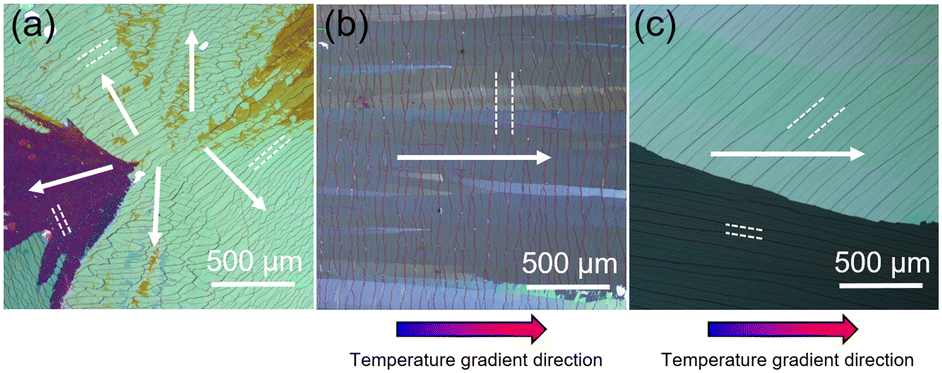 | ||
| Fig. 4 Ex situ POM images for the samples (a) cooling from a uniform temperature of 120 °C, (b) 110–120 °C temperature gradient, and (c) 107–117 °C temperature gradient. The image (a) is taken at around the nucleation point shown in Fig. 3(b). Direction of growth and cracks are denoted by white arrow and dashed line, respectively. | ||
The in-plane orientation of the C8-BTBT thin films was investigated by GIXD. Fig. 5(a) and (b) show in-plane reciprocal space maps for C8-BTBT thin films grown with temperature gradient with and without seeding. In both cases, 110, 020, 120, and 200 diffractions are clearly observed,29 however, the φ distribution of the diffraction spots is different (note that as-deposited film without annealing shows no preferential orientation as shown in Fig. S4†). In the temperature gradient growth without seeding, the diffraction spots are not sharp and distributed in φ angle, indicating a weak in-plane orientation (Fig. 5(a)). By overlaying the in-plane reciprocal lattice on the map (white lines), drawn so that b* is parallel to φ = −4° (where the strongest spot is observed), the pattern can be explained by the diffractions from the domains with the in-plane orientation distribution of ∼20° as denoted by red lines. This growth is like a spherulitic growth mode which is reported post-anneal crystallization of rubrene thin films via amorphous phase.40 The observed φ angle and its distribution of 020 diffraction in the reciprocal space are almost consistent with the crack angles observed in the film, which formed perpendicular to the growth direction (which is almost parallel to the temperature gradient direction) as shown in Fig. 5c. This result agrees with the previous report on zone-casted C8-BTBT films where the cracking is most likely occurred along the (010) plane because of the anisotropy of thermal expansion coefficient (see note in ESI†).41 Thus, in this growth process, which is based on the spontaneous nucleation and high rate growth without seeding, the in-plane orientation is determined by the growth direction which is almost parallel to the temperature gradient direction. Similar growth behaviour is reported on the C8-BTBT thin films prepared by off-centre spin-coating11 and temperature gradient growth after spin-coating.26
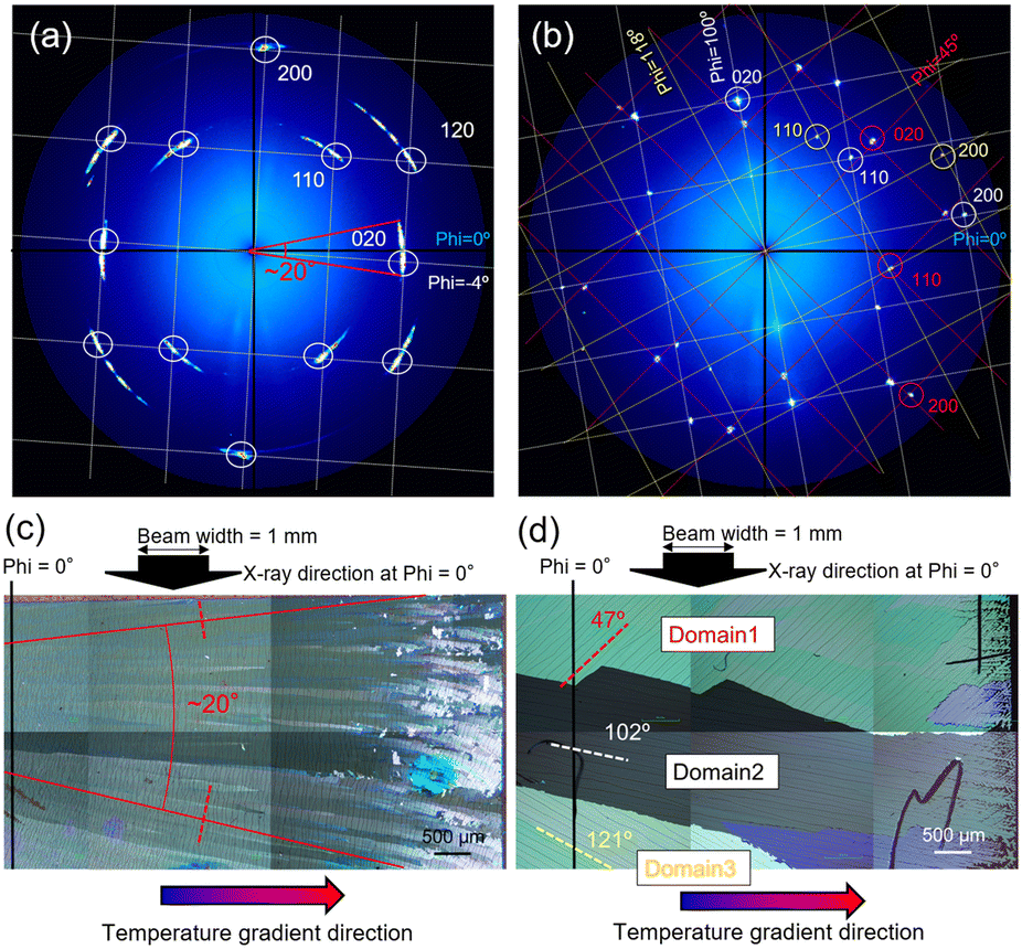 | ||
| Fig. 5 In-plane reciprocal space maps for C8-BTBT thin films grown with temperature gradient (a) with and (b) without seeding. (c) and (d) are corresponding stitched POM images for (a) and (b) showing the X-ray beam direction at Phi = 0° (black arrow) and crack directions (dashed line). | ||
On the other hand, in the sample grown with the temperature gradient with seeding, sharp diffraction spots were observed (Fig. 5b), indicating a strong in-plane orientation. This pattern can be explained well by the diffractions from three domains with different in-plane angles, which shows 020 diffractions at φ = 45°, 100°, and 118°. These crystallographic orientation angles are consistent with the angle of cracks in three domains as shown in the ex situ POM image (Fig. 5d). This result indicates that, in the low rate growth with seeding, the in-plane orientation of these domains is not determined by the growth direction but rather by the orientation of the seed crystals.
3.3 Control of crystallization rate by seeded temperature gradient cooling
When the crystallization of C8-BTBT thin films was carried out without seeding, the growth rate tends to be very high (∼880 and ∼780 μm s−1 for uniform and gradient temperature growth, respectively) as described in the previous section. It is because all the part of the thin film is in a large supercooling state before the crystallization (Fig. 3(a) and (c)) and thus the crystallization rate would be determined by the kinetic coefficient of crystallization rate, which is relevant to the diffusion coefficient of molecules in the precursor phase (supercooled liquid crystalline phase).42 On the other hand, when the crystallization was carried out from seed crystals with the temperature gradient, the large supercooling can be prevented (Fig. 3(e)), and moreover, the growth rate can be controlled by the cooling rate with keeping the temperature gradient constant and the degree of temperature gradient in the substrate. In this case, without taking account of the supercooling, the designed growth rate Vgr_des (μm s−1) was calculated as follows:where R is cooling rate (°C min−1); Tgrad is temperature gradient in the substrate (°C mm−1).
Here, we investigate temperature gradient growth with seeding at six different R of 0.03, 0.1, 1, 5, 10, and 16.5 °C min−1, and the constant Tgrad of 0.91 °C mm−1. The designed growth rate calculated from the equation above and the observed designed growth rate estimated from the in situ POM observation were compared in Fig. 6. As a result, a proportional relationship was confirmed between the designed and the observed growth rate, indicating that the growth rate was controlled intentionally by the gradient growth parameters (R and Tgrad in the substrate). It should be noted that the deviation from an ideal situation can be explained by the difference between the temperature indicated by the thermocouples attached on the aluminium stages and the actual surface temperature of the substrate so that the temperature gradient in the substrate was smaller than the expected value. This would result in the higher observed growth rates than the designed values.
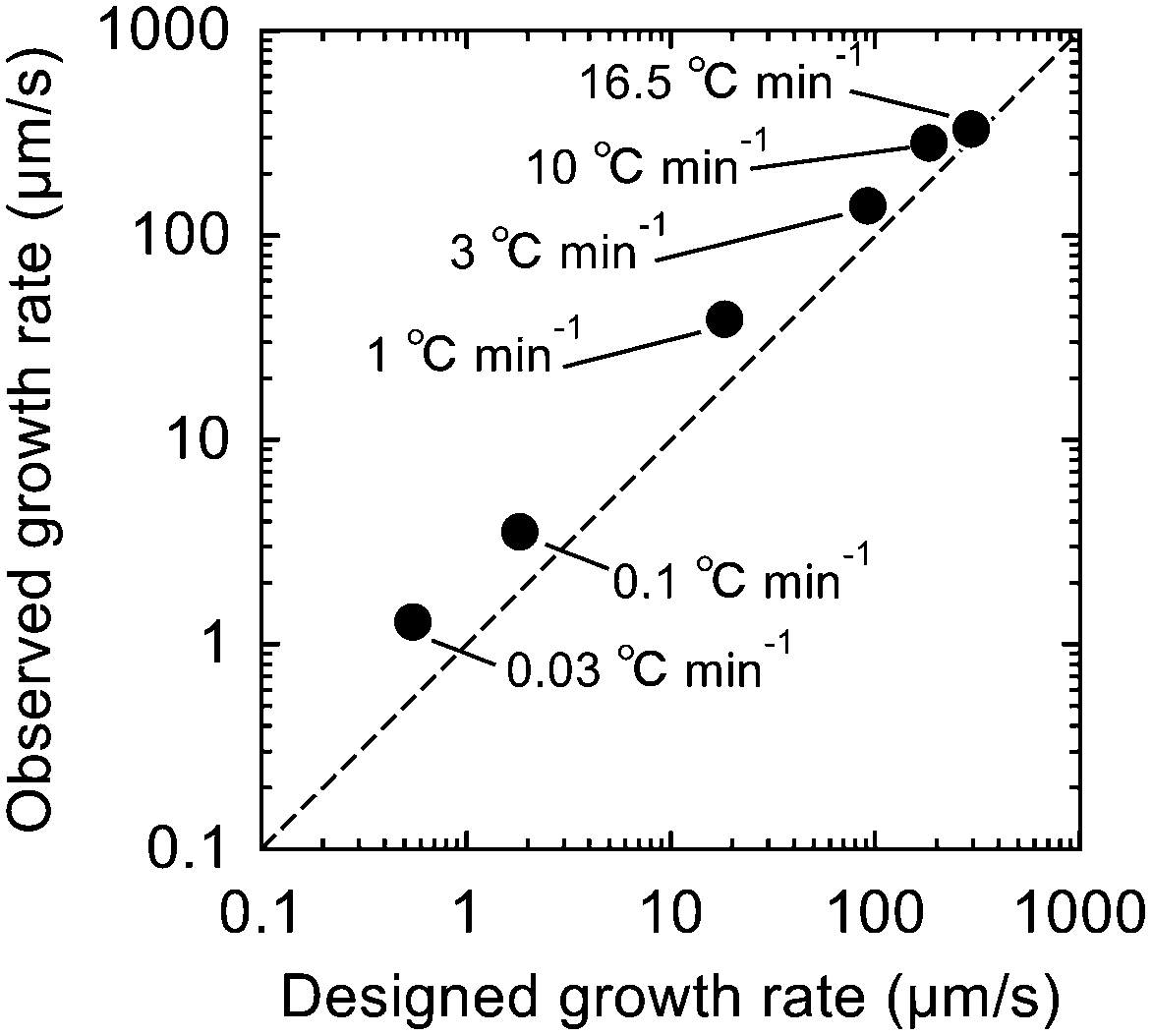 | ||
| Fig. 6 Comparison of designed and experimental growth rate for the temperature gradient growth with seeding. The dashed line indicates an ideal situation (designed Vcr is equals to observed Vcr). | ||
It should be noted that, even for the seeded temperature gradient crystallization, the cracking direction, i.e. (010) plane, tends to be perpendicular to the growth direction when the high cooling rate (high growth rate) which is similar to the case without seeding (Fig. 4(b) and 5(c)), while it reflects the orientation of seed crystals for the sample grown with low cooling rate (low growth rate) as shown in Fig. S5.† This would be due to the spontaneous nucleation occurring ahead of the growth front of the crystal grown from the seed crystals (because of the high cooling rate), resulting in a growth mode in which the crystal orientation is determined by the growth direction as described in the previous section. This result indicates that the cooling rate should be low enough to promote the crystal growth from seeds with avoiding spontaneous nucleation.
3.4 OFET performance
To evaluate the electrical property of the C8-BTBT thin films grown by the seeded temperature gradient method, we fabricated top-contact/bottom-gate planar type OFETs of a C8-BTBT film with a single domain in the channel, which was ensured by POM observation. Since the hole transport property of C8-BTBT is anisotropic, reflecting that the transfer integral along the a-axis is much larger than those along the b-axis,43 the mobility measured by OFET (the field effect mobility) depends on the in-plane orientation of the domain relative to the channel direction defined by the source-drain electrodes. Since we can estimate the in-plane orientation of a domain by the crack direction (cracking occurred along a-axis) as discussed in section 3.2, we plotted the observed mobility against the crack angle with respect to the direction perpendicular to the channel direction (Fig. 7). As a result, mobility was increased with the crack angle, which is consistent with the previous report.25 When the crack angle is close to 0°, b-axis is parallel to the channel direction. In this case, not only an intrinsic effect of crystal orientation that matches the non-preferential hole transport direction (b-axis) in C8-BTBT crystal but also an extrinsic effect of the cracks, which formed in a way to interrupt the current flow, would result in the lower mobility. In fact, at least one crack was in the channel. In contrast, the crack angle is close to 90°, the a-axis is parallel to the channel direction so that those intrinsic and extrinsic effects will be minimized, resulting in higher mobility. However, the samples with the crack angle of 90° show comparable mobilities with the sample deposited at RT, even though they have the in-plane orientation expected to show better transport property compared to the RT deposited film, which consists of randomly in-plane oriented domains (Fig. S4†). This might be due to that the cracks are not exactly straight (Fig. 4(c)) and/or insufficient strain release during the heat shrinkage process after the post-anneal crystallization, resulting in the suppression of charge transport. Note that the devices with shorter channel lengths tend to be showing lower the mobility. This can be due to the effect of contact resistance at source and drain electrodes which reduces the apparent field-effect mobility in short channel length devices.44–46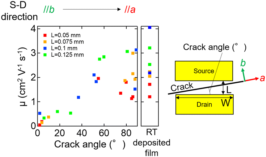 | ||
| Fig. 7 Crack angle dependence of mobility with different channel lengths (L) for the C8-BTBT thin films grown by temperature gradient with seeding, together with the mobility of the thin film deposited at RT for comparison. Definition of crack angle is shown in right. | ||
Conclusions
We have demonstrated the large domain crystal growth of vapor-deposited C8-BTBT thin films on SiO2/Si substrate from liquid crystal state by seeded temperature gradient cooling crystallization using a custom-made substrate holder. In this process, the direction of crystallization was defined by the temperature gradient. When there is no seed crystal before crystallization, the high-speed crystal growth was taken place because that the growth was occurred from a large supercooling with spontaneous nucleation, resulting in the spherulitic growth mode. On the other hand, by providing crystal seeds at the low-temperature side, the growth rate was intentionally controlled by the cooling rate and temperature gradient in the substrate. In this case, when the cooling rate is low enough so that no spontaneous nucleation is occurred, the growth started from the seeds and thereby the in-plane orientation of the crystal is defined by the orientation of seeds. Moreover, the geometrical selection during the growth results in the formation of large single-crystal domains. Therefore, this approach will be promising for the preparation of orientation-controlled single-crystal uniform organic thin films by vacuum deposition if two remaining challenges can be overcome: 1) selection of a seed crystal with a specific orientation and 2) reduction of cracks in the thin film.Conflicts of interest
There are no conflicts to declare.Acknowledgements
This work was supported by a Grant-in-Aid for Scientific Research (No. 19H02589, 22H01946) from the Ministry of Education, Culture, Sports, Science, and Technology of Japan. The GIXD experiments were performed at SPring-8 with the approval of the Japan Synchrotron Radiation Research Institute (JASRI) (Proposal No. 2020A1881).References
- G. Horowitz, J. Mater. Res., 2004, 19, 1946–1962 CrossRef CAS.
- A. Di Carlo, F. Piacenza, A. Bolognesi, B. Stadlober and H. Maresch, Appl. Phys. Lett., 2005, 86, 263501 CrossRef.
- R. Matsubara, N. Ohashi, M. Sakai, K. Kudo and M. Nakamura, Appl. Phys. Lett., 2008, 92, 242108 CrossRef.
- M. Nakamura, H. Ohguri, N. Goto, H. Tomii, M. Xu, T. Miyamoto, R. Matsubara, N. Ohashi, M. Sakai and K. Kudo, Appl. Phys. A: Mater. Sci. Process., 2009, 95, 73–80 CrossRef CAS.
- A. Tracz, J. K. Jeszka, M. D. Watson, W. Pisula, K. Müllen and T. Pakula, J. Am. Chem. Soc., 2003, 125, 1682–1683 CrossRef CAS PubMed.
- W. Pisula, A. Menon, M. Stepputat, I. Lieberwirth, U. Kolb, A. Tracz, H. Sirringhaus, T. Pakula and K. Müllen, Adv. Mater., 2005, 17, 684–689 CrossRef CAS.
- G. Giri, E. Verploegen, S. C. B. Mannsfeld, S. Atahan-Evrenk, D. H. Kim, S. Y. Lee, H. A. Becerril, A. Aspuru-Guzik, M. F. Toney and Z. Bao, Nature, 2011, 480, 504–508 CrossRef CAS PubMed.
- J. Soeda, Y. Hirose, M. Yamagishi, A. Nakao, T. Uemura, K. Nakayama, M. Uno, Y. Nakazawa, K. Takimiya and J. Takeya, Adv. Mater., 2011, 23, 3309–3314 CrossRef CAS.
- H. Minemawari, T. Yamada, H. Matsui, J. Tsutsumi, S. Haas, R. Chiba, R. Kumai and T. Hasegawa, Nature, 2011, 475, 364–367 CrossRef CAS PubMed.
- Z. Wang, H. Guo, J. Li, L. Wang and G. Dong, Adv. Mater. Interfaces, 2019, 6, 1801736 CrossRef.
- Y. Yuan, G. Giri, A. L. Ayzner, A. P. Zoombelt, S. C. B. Mannsfeld, J. Chen, D. Nordlund, M. F. Toney, J. Huang and Z. Bao, Nat. Commun., 2014, 5, 3005 CrossRef PubMed.
- S. Arai, S. Inoue, T. Hamai, R. Kumai and T. Hasegawa, Adv. Mater., 2018, 30, 1707256 CrossRef.
- G. Kitahara, S. Inoue, T. Higashino, M. Ikawa, T. Hayashi, S. Matsuoka, S. Arai and T. Hasegawa, Sci. Adv., 2020, 6, eabc8847 CrossRef CAS PubMed.
- Q. Wang, E. J. Juarez-Perez, S. Jiang, M. Xiao, J. Qian, E.-Y. Shin, Y.-Y. Noh, Y. Qi, Y. Shi and Y. Li, Phys. Rev. Mater., 2020, 4, 044604 CrossRef CAS.
- W. Deng, Y. Xiao, B. Lu, L. Zhang, Y. Xia, C. Zhu, X. Zhang, J. Guo, X. Zhang and J. Jie, Adv. Mater., 2021, 33, 2005915 CrossRef CAS PubMed.
- R. Ruiz, D. Choudhary, B. Nickel, T. Toccoli, K.-C. Chang, A. C. Mayer, P. Clancy, J. M. Blakely, R. L. Headrick, S. Iannotta and G. G. Malliaras, Chem. Mater., 2004, 16, 4497–4508 CrossRef CAS.
- P. W. Bridgman, Proc. Am. Acad. Arts Sci., 1925, 60, 305 CrossRef.
- D. C. Stockbarger, Rev. Sci. Instrum., 1936, 7, 133–136 CrossRef CAS.
- G. Gbabode, N. Dumont, F. Quist, G. Schweicher, A. Moser, P. Viville, R. Lazzaroni and Y. H. Geerts, Adv. Mater., 2012, 24, 658–662 CrossRef CAS PubMed.
- B. Chattopadhyay, L. Jacobs, P. Panini, I. Salzmann, R. Resel and Y. Geerts, Cryst. Growth Des., 2018, 18, 1272–1277 CrossRef CAS.
- P. Panini, B. Chattopadhyay, O. Werzer and Y. Geerts, Cryst. Growth Des., 2018, 18, 2681–2689 CrossRef CAS.
- G. Schweicher, N. Paquay, C. Amato, R. Resel, M. Koini, S. Talvy, V. Lemaur, J. Cornil, Y. Geerts and G. Gbabode, Cryst. Growth Des., 2011, 11, 3663–3672 CrossRef CAS.
- G. Liu, J. Liu, A. S. Dunn, P. Nadazdy, P. Siffalovic, R. Resel, M. Abbas, G. Wantz and Y. H. Geerts, Cryst. Growth Des., 2021, 21, 5231–5239 CrossRef CAS.
- G. Schweicher, G. Liu, P. Fastré, R. Resel, M. Abbas, G. Wantz and Y. H. Geerts, Mater. Chem. Front., 2021, 5, 249–258 RSC.
- T. Hoshino, H. Ito, I. Fujieda and T. Hanasaki, Proc. SPIE, 2013, 8831, 8831151 CrossRef.
- I. Fujieda, N. Iizuka and Y. Onishi, Proc. SPIE, 2015, 9360, 936012 CrossRef.
- J.-H. Kim, S. Han, H. Jeong, H. Jang, S. Baek, J. Hu, M. Lee, B. Choi and H. S. Lee, ACS Appl. Mater. Interfaces, 2017, 9, 9910–9917 CrossRef CAS PubMed.
- H. Ebata, T. Izawa, E. Miyazaki, K. Takimiya, M. Ikeda, H. Kuwabara and T. Yui, J. Am. Chem. Soc., 2007, 129, 15732–15733 CrossRef CAS.
- T. Izawa, E. Miyazaki and K. Takimiya, Adv. Mater., 2008, 20, 3388–3392 CrossRef CAS.
- M. Dohr, H. M. A. Ehmann, A. O. F. Jones, I. Salzmann, Q. Shen, C. Teichert, C. Ruzié, G. Schweicher, Y. H. Geerts, R. Resel, M. Sferrazza and O. Werzer, Soft Matter, 2017, 13, 2322–2329 RSC.
- H. Komatsu, M. Tanaka, K. Kaminaga, S. Maruyama and Y. Matsumoto, Chem. Lett., 2022, 51, 162–165 CrossRef CAS.
- M. F. Ramananarivo, T. Higashi, M. Ohmori, K. Sudoh, A. Fujii and M. Ozaki, Appl. Phys. Express, 2016, 9, 061601 CrossRef.
- T. Kitagawa, M. F. Ramananarivo, A. Fujii and M. Ozaki, Jpn. J. Appl. Phys., 2018, 57, 04FL09 CrossRef.
- T. Kitagawa, M. Fujisaki, S. Nagano, N. Tohnai, A. Fujii and M. Ozaki, Appl. Phys. Express, 2019, 12, 051011 CrossRef CAS.
- L. Yu, M. R. Niazi, G. O. Ngongang Ndjawa, R. Li, A. R. Kirmani, R. Munir, A. H. Balawi, F. Laquai and A. Amassian, Sci. Adv., 2017, 3, e1602462 CrossRef.
- S. Yaginuma, K. Itaka, M. Haemori, M. Katayama, K. Ueno, T. Ohnishi, M. Lippmaa, Y. Matsumoto and H. Koinuma, Appl. Phys. Express, 2008, 1, 015005 CrossRef.
- S. Maruyama, Y. Takeyama, H. Taniguchi, H. Fukumoto, M. Itoh, H. Kumigashira, M. Oshima, T. Yamamoto and Y. Matsumoto, ACS Nano, 2010, 4, 5946–5952 CrossRef CAS.
- T. Miyadera, Y. Auchi, T. Koganezawa, H. Yaguchi and M. Chikamatsu, APL Mater., 2020, 8, 041104 CrossRef CAS.
- P. L. Krapivsky, L. I. Nazarov and M. V. Tamm, J. Stat. Mech.: Theory Exp., 2019, 2019, 073206 CrossRef.
- T. R. Fielitz and R. J. Holmes, Cryst. Growth Des., 2016, 16, 4720–4726 CrossRef CAS.
- P. Fesenko, C. Rolin, R. Janneck, S. P. Bommanaboyena, H. Gaethje, P. Heremans and J. Genoe, Org. Electron., 2016, 37, 100–107 CrossRef CAS.
- M. Uwaha, in Handbook of Crystal Growth, ed. T. Nishinaga, Elsevier, Boston, 2nd edn, 2015, pp. 359–399 Search PubMed.
- H. Minemawari, M. Tanaka, S. Tsuzuki, S. Inoue, T. Yamada, R. Kumai, Y. Shimoi and T. Hasegawa, Chem. Mater., 2017, 29, 1245–1254 CrossRef CAS.
- T. Uemura, C. Rolin, T.-H. Ke, P. Fesenko, J. Genoe, P. Heremans and J. Takeya, Adv. Mater., 2016, 28, 151–155 CrossRef CAS PubMed.
- M. Marinkovic, D. Belaineh, V. Wagner and D. Knipp, Adv. Mater., 2012, 24, 4005–4009 CrossRef CAS PubMed.
- R. Wawrzinek, J. Sobus, M. U. Chaudhry, V. Ahmad, A. Grosjean, J. K. Clegg, E. B. Namdas and S.-C. Lo, ACS Appl. Mater. Interfaces, 2019, 11, 3271–3279 CrossRef CAS.
Footnote |
| † Electronic supplementary information (ESI) available. See DOI: https://doi.org/10.1039/d2ce01280d |
| This journal is © The Royal Society of Chemistry 2023 |