
 Open Access Article
 This Open Access Article is licensed under a Creative Commons Attribution-Non Commercial 3.0 Unported Licence
Soft landing of polyatomic anions onto three-dimensional semiconductive and conductive substrates†
Habib
Gholipour-Ranjbar
 a,
Hang
Hu
a,
Pei
Su
a,
Hugo Yuset
Samayoa Oviedo
a,
Christopher
Gilpin
c,
Haomin
Wang
b,
Yingying
Zhang
b and
Julia
Laskin
*a
a,
Hang
Hu
a,
Pei
Su
a,
Hugo Yuset
Samayoa Oviedo
a,
Christopher
Gilpin
c,
Haomin
Wang
b,
Yingying
Zhang
b and
Julia
Laskin
*a
aDepartment of Chemistry, Purdue University, West Lafayette, IN 47906, USA. E-mail: jlaskin@purdue.edu
bDepartment of Chemistry, Key Laboratory of Organic Optoelectronics and Molecular Engineering of the Ministry of Education, Tsinghua University, Beijing 100084, China
cLife Science Microscopy Facility, Purdue University, West Lafayette, IN 47907, USA
First published on 16th February 2023
Abstract
Soft landing of well-characterized polyoxometalate anions, PW12O403− (WPOM) and PMo12O403− (MoPOM), was carried out to explore the distribution of anions in the semiconducting 10 and 6 μm-long vertically aligned TiO2 nanotubes as well as 300 μm-long conductive vertically aligned carbon nanotubes (VACNTs). The distribution of soft-landed anions on the surfaces and their penetration into the nanotubes were studied using energy dispersive X-ray spectroscopy (EDX) and scanning electron microscopy (SEM). We observe that soft landed anions generate microaggregates on the TiO2 nanotubes and only reside in the top 1.5 μm of the nanotube height. Meanwhile, soft landed anions are uniformly distributed on top of VACNTs and penetrate into the top 40 μm of the sample. We propose that both the aggregation and limited penetration of POM anions into TiO2 nanotubes is attributed to the lower conductivity of this substrate as compared to VACNTs. This study provides first insights into the controlled modification of three dimensional (3D) semiconductive and conductive interfaces using soft landing of mass-selected polyatomic ions, which is of interest to the rational design of 3D interfaces for electronics and energy applications.
Introduction
Surface functionalization using well-defined nanoclusters (NCs) has attracted considerable attention in catalysis and materials science due to the distinct properties of atomically-precise NCs as compared to nanoparticles of a similar composition.1–3 Different types of NCs deposited onto surfaces have demonstrated fascinating performance in oxidative dehydrogenation,4 energy storage,5 sub-surface imaging of 2D materials,6 electrocatalytic water oxidation,7,8 and lithium–air batteries.9,10 As a result, there is a considerable interest to the preparation of uniformly distributed NCs on semiconductive and conductive substrates for the design of new technological interfaces with desirable electrochemical, optical, or electronic properties.Interactions of gas-phase ions with surfaces have been used in ion implantation, physical and chemical sputtering, surface-induced dissociation (SID), and soft landing experiments.11–16 These processes exploit the ability to accelerate ions in vacuum to a defined kinetic energy (KE), which determines the outcome of ion-surface collisions. By controlling the KE of the ions, the competition between ion deposition, implantation, sputtering, desorption, dissociation by collisions with the surface, or chemical reactivity with surface material may be readily controlled.17–19 For example, high energy ions (>103 eV) are used for ion implantation or sputtering.17 Meanwhile, hyperthermal energy collisions (<100 eV) are dominated by the competition between ion soft landing, scattering, and SID.19 Ion soft landing is a mass spectrometry-based technique, which enables intact deposition of pure ions of known composition, charge state, and kinetic energy on either conductive or semiconductive substrates.14,18–25 This method has been used to generate high-purity ultrathin layers with unsurpassed selectivity thereby providing surface preparation capabilities, which are currently inaccessible using conventional deposition methods. Although ion soft landing has been predominately used for preparing ultrathin layers of molecular ions on model surfaces including self-assembled monolayers (SAMs),26–29 highly oriented pyrolytic graphite (HOPG),30 pure metal substrates,31 and glassy carbon,32 recent studies have demonstrated the potential of this precisely-controlled preparative technique for the design of technologically-relevant interfaces and device fabrication.33,34 These applications have been enabled by the development of high-flux ion soft landing instrumentation,35 which is a promising tool for the design of functional 3D interfaces.36,37 However, little is known about the distribution of soft-landed ions in conductive and semiconductive 3D interfaces, which are of interest to applications in catalysis, energy storage, and separations.
In this study, we examine the penetration of soft-landed ions into two model 3D materials: a substrate composed of 10 and 6 μm-long vertically aligned TiO2 nanotubes (NTs) as a semiconducting substrate and a conductive substrate composed of 300 μm-long vertically aligned carbon nanotubes (VACNT). Both TiO2 NTs and VACNTs are attractive materials for applications in energy storage and electronics and are well-suited for studying the distribution of soft-landed ions along the depth of 3D interfaces.38–42 This study provides insights into the design and functionalization of semiconductive and conductive 3D materials using well-defined ions.
Experimental
Preparation of TiO2 NTs and VACNTs
Substrates containing 10 μm-long TiO2 NTs were prepared using a two-step anodization of a Ti foil (thickness 0.127 mm, 99.7% trace metals basis, Sigma Aldrich) in an electrolyte composed of 96.7% of ethylene glycol (EG), 3% of deionized (DI) water, and 0.3% of ammonium fluoride (NH4F). Briefly, 0.16 g NH4F was dissolved in 1.5 mL of DI water and 48.5 mL of EG was added to the solution and mixed for 10 min to obtain a uniform electrolyte solution. A two-electrode system was used for applying the anodization voltage in the range of 0–60 V with a limiting current of 0–0.5 A using a DC power supply (E3612A, Agilent). In this system, the Ti foil (0.5 cm × 1 cm) was connected to the anode (positive electrode) and a graphite rod served as a cathode (negative electrode). Anodization was performed by applying a 60 V potential to the anode for 2 h with the cathode connected to the ground potential. An oxide layer generated on the surface of the Ti foil was dried and removed from the surface by blowing the N2 gas resulting in a shiny and clean Ti foil substrate. The clean Ti substrate underwent a second anodization step at 60 V for 30 min to generate vertically aligned TiO2 NTs. All the anodization processes were performed at room temperature while the solution was stirred slowly using the magnetic stirrer bar to keep the composition of the electrolyte uniform during the anodization. The prepared TiO2 NTs were washed in deionized (DI) water, sonicated for 5 min in water to remove impurities, and dried at room temperature. A substrate containing 6 μm-long TiO2 NTs was prepared using the same procedure. The only difference is the second anodization step which was 15 min at 60 V. The as synthesized TiO2 samples were annealed in air at 350 °C for 2.5 h to improve their conductivity and make them suitable for soft landing experiments. The resistance of the annealed samples was 50–70 kΩ measured using a digital multimeter (115 TRUE RMS, FLUKE). Meanwhile, before annealing, the substrates had an infinite resistance. The decrease in the resistance of TiO2 samples is attributed to the formation of the anatase form of TiO2 (according to the XRD of the annealed TiO2 sample shown in Fig. S1†), which has a lower resistance as compared to the amorphous TiO2.43 The annealed TiO2 NTs were used as a semiconducting substrate in ion soft landing experiments.The VACNT arrays were synthesized through the chemical vapor deposition (CVD) method in a quartz tube furnace, following protocols reported by Zhang et al.44
Ion soft landing experiments
The POM anions were soft-landed onto substrates using a custom-designed ion soft landing instrument described in detail in our previous study.45 As indicated earlier, all the soft landing experiments onto TiO2 NTs were performed using the annealed TiO2 substrates. A 150 μM solution of Na3[PW12O40]·H2O or Na3[PMo12O40]·H2O in methanol was transferred through a fused silica capillary (Polymicro, ID 51.5 μm, OD 149.8 μm) positioned in front of the instrument's heated inlet at a flow rate of 60 μL h−1 using a syringe pump (LEGATO 101, KD Scientific, Holliston, MA). POM anions are generated at the tip of the capillary by applying −3.0 kV to the syringe needle. Ions are subsequently transferred into a bent ion guide which bends the ion beam to eliminate droplets and neutral species from the instrument axis. Ions of interest are selected using a quadrupole mass filter (9.5 mm rod diameter, Extrel CMS, Pittsburgh, PA). A mass-selected ion beam is collimated using an einzel lens and transferred to a surface, positioned after the lens and connected to a picometer (RBD 9103 USB Picoammeter, RBD Instruments, Bend, OR), which measures ion current. Based on the measured ion current (∼6 nA on both VACNT and TiO2 NTs), we calculated ion coverage on surfaces as described in the ESI.† We note that ions are directed at the surface along the surface normal. As a result, the lateral component of the ion velocity is very small in our experiments.Typical voltages applied to different elements along the ion beam path optimized for WPOM and MoPOM analytes are as follows: peak-to-peak voltages of 180 V in the high-pressure funnel (HPF) and 65 V in the low-pressure funnel (LPF); DC bias of −8.0 V is applied to the bent flatapole rods, and the quadrupole mass filter is operated at a frequency of 555 kHz. The pressure in the soft landing chamber during ion deposition is 4 × 10⁻⁵ Torr.
Mass spectrometry analysis
All mass spectrometry analyses of the substrates after soft-landing were performed using an ion mobility quadrupole time-of-flight mass spectrometer (Agilent 6560 IM QTOF, Agilent technologies, Santa Clara, CA). The sample surface was washed with 150 μL of methanol. The resulting solution was introduced into the mass spectrometer. Ions were produced using a custom-designed ESI source operated in negative ion mode. In this source, a sample solution is delivered to a mass spectrometer inlet using a syringe pump (LEGATO 180, KD Scientific, Holliston, MA) through a fused silica capillary (OD 150 μm × ID 50 μm) at a flow rate of 0.3 μL min−1 and ionized by applying a high voltage of 3.5 kV to the instrument's inlet.Sample preparation for SEM and EDX analysis
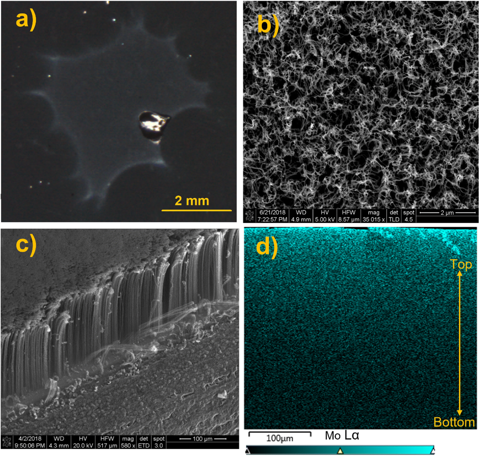
We used a field-emission scanning electron microscope (FEI Quanta 3D FEG Dual-Beam SEM, FEI Company, Hillsboro, OR) equipped with EDX for the characterization of both the pristine 3D materials and materials populated with soft-landed ions. The top sides of the samples were analyzed directly using SEM and EDX. In order to profile chemical gradients throughout the depth of the TiO2 NTs samples, we carefully peeled off a small area of the TiO2 NTs layers from the edge of the Ti substrate by gently bending the Ti/TiO2 substrates which detaches 10 μm TiO2 from the Ti substrates making cross sectional EDX analysis easier. In contrast with 10 μm TiO2 NT layer which detaches readily from the Ti substrate, 6 μm TiO2 NTs do not detach from the Ti substrate after bending as seen in its SEM image in Fig. S3.† Meanwhile, the cross section of the VACNT substrates was prepared by cutting a small section of the substrate using a sharp blade. The cleaved substrates were mounted onto a sample holder vertically such that the electron gun of the SEM is directed at the cross section of the substrates as shown in Fig. 1. The start and end point of the prepared cross sections for EDX line scan analysis is determined under SEM. As seen in Fig. S2† we selected the start and end point of the line scan under SEM to exactly target the bottom of TiO2/WPOM (not the Ti substrate) and the topmost point where NTs end.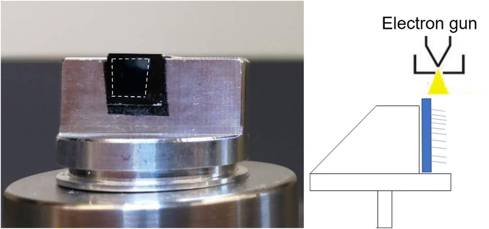 | ||
| Fig. 1 A photograph of the sample holder and a schematic drawing illustrating the mounting geometry used for the cross-section analysis of the substrates. The dashed line shows the location where the sample is mounted. | ||
We used Oxford Instruments Aztec software controlling a SDD EDX detector set at process time 3. The microscope was set at 20 kV spot size 5 with a working distance of 10 mm. Line scans were collected with 500 points over a line length of 10 μm. The results are semi quantitative. The resolution is dependent on spot size, accelerating voltage and the density of the sample. The depth that the beam penetrates is about 1.4 μm into Ti and about 0.35 μm in tungsten. We do not know the exact diameter of the beam. The microscope manufacture does not reveal this information.
Results and discussion
We synthesized vertically aligned TiO2 NTs substrates using a well-established anodization method46 with some modifications mentioned in the experimental part. Fig. 2 shows the SEM images of the prepared TiO2 NTs at different magnifications. SEM images obtained from the top of the substrate (Fig. 2a and b) show well-ordered NTs with the inner diameter of 100 nm. Fig. 2c and d shows the cross-sectional SEM images (Fig. 2c and d) of 10 μm TiO2 NTs after detaching them from the Ti substrate by carefully bending the Ti/TiO2 sample. These images exhibit NTs with the length of 10 μm that still preserve their order and integrity after being detached from the Ti substrate. In contrast, 6 μm TiO2 NTs do not detach from the substrate as shown in Fig. S3.†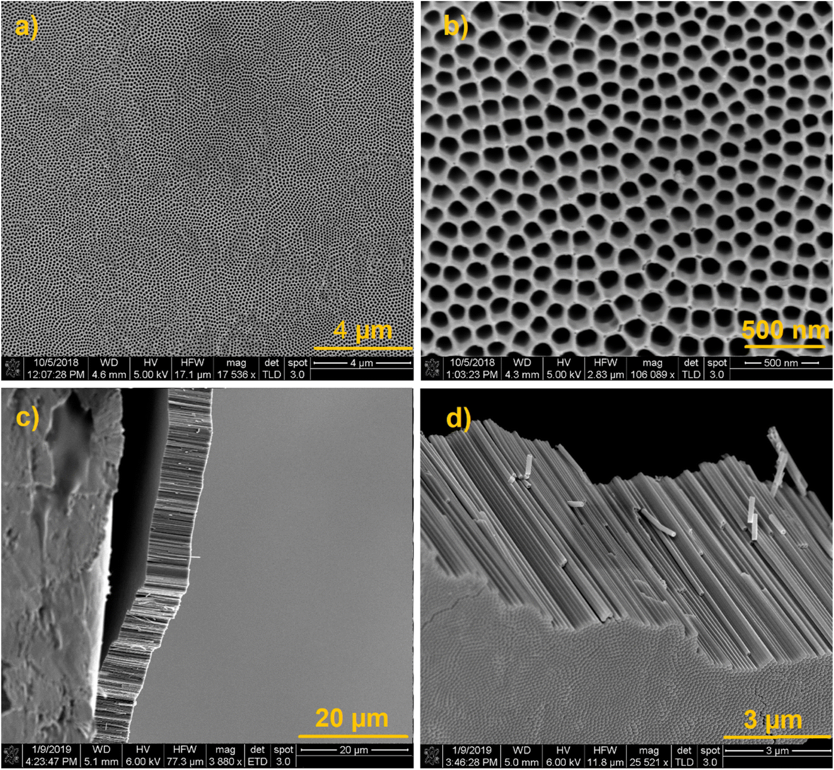 | ||
| Fig. 2 (a–d) SEM images of the synthesized highly ordered vertically aligned TiO2 NTs at different angles and magnifications. | ||
The EDX spectrum averaged over a line scan acquired on top of the TiO2 NT surface is shown in Fig. 3a. The spectrum confirms the presence of Ti and O elements in the top layer with a 2.4![[thin space (1/6-em)]](https://www.rsc.org/images/entities/char_2009.gif) :1 atomic ratio of O:Ti, which is greater than the expected O:Ti ratio of 2:1 for pure TiO2. The EDX line scan across the length of the pristine TiO2 NTs shown in Fig. 3b indicates that the atomic percentages (at%) of O and Ti atoms remain constant across the TiO2 NT with the expected atomic ratio of 2:1 for O:Ti in the bottom 6.5 μm of the NTs. However, the atomic percentage of O increases substantially and that of Ti decreases in the topmost 3.0 μm of the TiO2 NTs. Because annealing is performed in air, the topmost layers of the NTs are more exposed to oxygen and are expected to be oxygen-rich. The increase in the O:Ti ratio in the topmost layer of TiO2 NTs may be due to the presence of anionic TiO3 or TiO4.47,48 EDX analysis confirms that the as-synthesized NT arrays are composed of pure titanium oxide with a greater atomic percentage of oxygen than in pure TiO2 in the topmost 3.0 μm of the TiO2 NTs.
:1 atomic ratio of O:Ti, which is greater than the expected O:Ti ratio of 2:1 for pure TiO2. The EDX line scan across the length of the pristine TiO2 NTs shown in Fig. 3b indicates that the atomic percentages (at%) of O and Ti atoms remain constant across the TiO2 NT with the expected atomic ratio of 2:1 for O:Ti in the bottom 6.5 μm of the NTs. However, the atomic percentage of O increases substantially and that of Ti decreases in the topmost 3.0 μm of the TiO2 NTs. Because annealing is performed in air, the topmost layers of the NTs are more exposed to oxygen and are expected to be oxygen-rich. The increase in the O:Ti ratio in the topmost layer of TiO2 NTs may be due to the presence of anionic TiO3 or TiO4.47,48 EDX analysis confirms that the as-synthesized NT arrays are composed of pure titanium oxide with a greater atomic percentage of oxygen than in pure TiO2 in the topmost 3.0 μm of the TiO2 NTs.
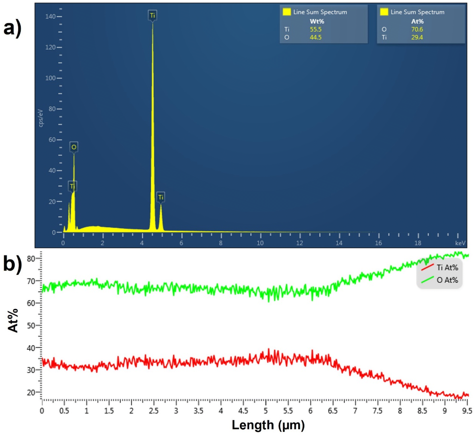 | ||
| Fig. 3 (a) The EDX spectrum of the TiO2 NTs; the elemental composition in both the atomic (at%) and weight (wt%) percentages are shown in the inset. (b) EDX line scans across the length of pristine TiO2. The results are expressed in terms of atomic percentages of the elements. | ||
The annealed TiO2 NTs were used as a surface for ion soft landing to investigate how anionic species populate 3D semiconducting interfaces. In these experiments, we used well-characterized PW12O403− (WPOM) anions. The dark field microscopy image of the WPOM soft landed on the TiO2 NTs with the coverage of 3.0 × 10¹⁴ ions (480 ng) is shown in Fig. 4a. The middle of the deposition spot, which has a higher concentration of anions appears blue in the image. The color of the deposition spot may be attributed to the formation of larger particles as a result of the dewetting process described in our previous study.27 In that study we demonstrated that anions on surfaces attract neutral molecules present in the background of the vacuum system and generate metastable layers that are stabilized by interactions with image charge in the underlying surface. When the layer is exposed to air, it uptakes water molecules. Water uptake initiates the dewetting process. According to the dewetting theory, depending on the thickness of the layer, it can be stable, unstable, or metastable. Both the kinetics and mechanism of the dewetting process are affected by the thickness of the layer as described in ref. 49. Given that the ion beam has a Gaussian shape with more ions in the middle of the ion beam, the center of the deposition spot has more anions and consequently more dewetting. Therefore, the dewetting process generates particles of different size depending on surface coverage. These particles interact differently with light resulting in a different color of the center and edges of the deposition spot. The SEM image of the sample (Fig. 4b) shows the presence of micron-size aggregates on top of the TiO2 NT substrate. Meanwhile, EDX mapping analysis of the aggregates (Fig. 4c and d) indicates that their composition is dominated by oxygen (O) and tungsten (W) confirming the formation of WPOM aggregates on the TiO2 NT surface. We note that aggregate islands form randomly in some parts of the deposition area. The small size of the aggregates did not allow us to target them using EDX line scan analysis of the cross section of the TiO2 NT surface. Additional SEM images shown in Fig. S4† indicate that there are other areas covered by WPOM that do not contain aggregates.
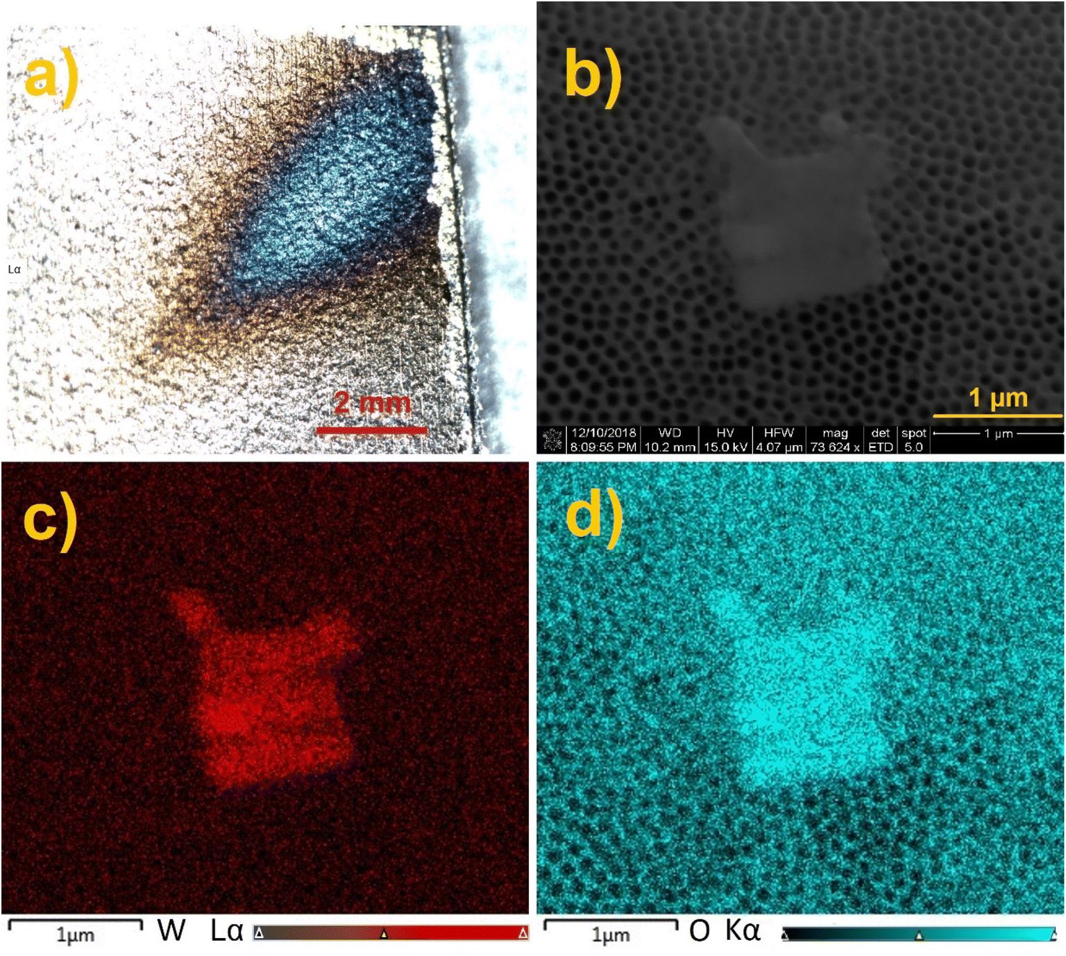 | ||
| Fig. 4 (a) A dark filed microscopy image, (b) SEM image, (c) EDX mapping of tungsten (W), and (d) EDX mapping of oxygen (O) in the TiO2 NTs substrate containing WPOM at a coverage of 3 × 10¹⁴ ions (480 ng). | ||
In order to quantify the penetration of soft-landed anions into the 3D 10 μm TiO2 NTs substrate, we performed EDX analysis of the cross section of the substrate prepared by soft landing of 3.0 × 10¹⁴ ions (480 ng) of WPOM. The results of this analysis are summarized in Fig. 5 both in terms of weight percentage and atomic percentage of different elements along the length of TiO2 NTs. The EDX line scan of this sample shows a similar trend in the O:Ti ratio across the NTs as the pristine TiO2 (as seen in Fig. 3b). In this sample, the O:Ti ratio increases in the topmost 3.0 μm of the substrate. In addition, a signal corresponding to W atoms of WPOM appears at 8.5 μm and increases towards the top of the substrate. This is more noticeable in Fig. 5a because the weight percentage of W is higher than its atomic percentage.
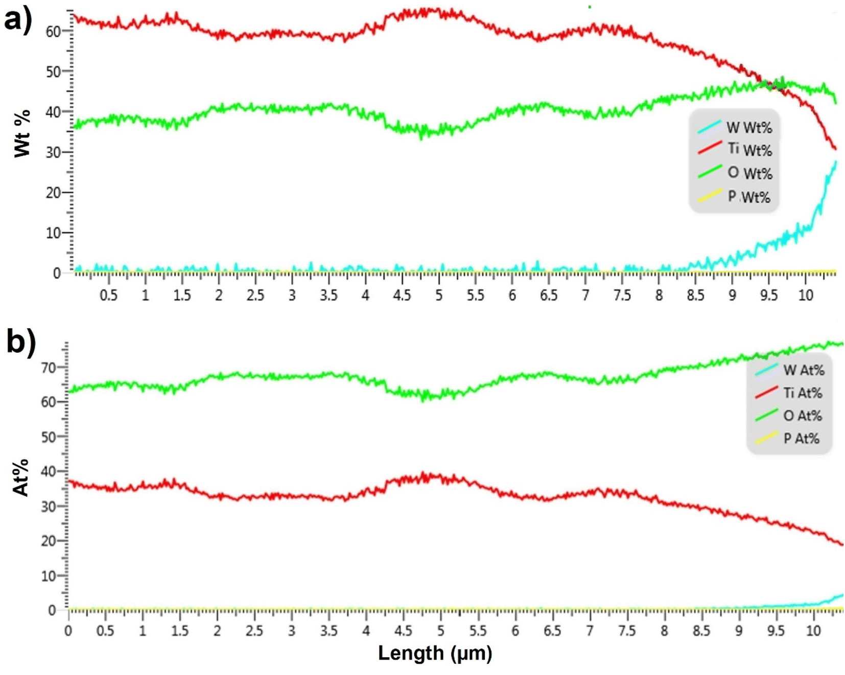 | ||
| Fig. 5 EDX line scans across the length of TiO2 NTs prepared by soft landing of 3 × 10¹⁴ ions (480 ng) of WPOM (a) in terms of weight percentage (wt%) (b) in terms of atomic percentage (at%) versus the length of NTs. | ||
Similar penetration depth of WPOM is observed in shorter TiO2 NTs (6 μm) as shown in Fig. S5 and S6† confirming that the penetration depth is rather independent of the length of the NTs. These observations indicate that WPOM penetrates only into the top 1.5 μm of the TiO2 NTs substrate. To demonstrate the reproducibility of the WPOM penetration into the TiO2 NTs, we acquired multiple EDX line scans in the vicinity of the target cross section for 6 μm TiO2/WPOM. As seen in the Fig. S5 and S6,† the peak corresponding to WPOM is observed in the topmost 1–2 μm of the NTs. Additionally, the ratio of O:Ti throughout the 6 μm TiO2 is slightly higher compared to the value obtained for 10 μm TiO2. However, similar penetration profiles of POM anions showing that they reside on the topmost 1–2 μm of the NTs were observed for both longer and shorter TiO2. We believe that soft-landed ions are deposited both onto the rims and inside the NTs. Because the diameter of the NTs (100 nm) is much greater than the thickness of the nanotube's rim (10 nm), a substantial fraction of the soft-landed ions likely “fly” inside the NTs until they hit the wall. However, because of the relatively high resistivity of TiO2, we anticipate that soft landed POM anions generate a potential that slows down the ions and prevents them from penetrating deeper into the layer. The formation of microaggregates on top of the layer supports this assertion.
Surface analysis of the TiO2/WPOM sample using mass spectrometry shows the presence of the triply and doubly charged WPOM anions (Fig. S7a†) confirming their intact deposition onto the TiO2 surface.
The EDX line scan obtained for another 10 μm TiO2 NTs sample after soft landing of 6.2 × 10¹⁴ WPOM anions (960 ng) (Fig. S8 (at%) and S2 (wt%)†) shows that, even with a substantially higher coverage, WPOM only penetrate into 1.0–1.5 μm of the TiO2 NTs topmost layer. Moreover, the SEM image of this sample shows the formation of larger aggregates on the surface (Fig. S9†). It follows that the depth of penetration of POM anions into TiO2 NTs is not affected to a significant extent by the coverage. Meanwhile, the aggregation of POM on top of the surface is coverage-dependent. The limited penetration depth of anions into the 3D TiO2 NTs may be attributed to its relatively low conductivity, which may result in charging up of the layer containing stable anions. Specifically, it has been demonstrated that oxygen-rich titanium oxides including TiO3 have a lower conductivity than TinO2n−1, n = 3, 4 and 5.50,51 It is reasonable to assume that the top layer of the annealed TiO2 NT substrate has a lower conductivity than the rest of the sample, which could rationalize the observed aggregation and limited penetration of WPOM into the oxygen-rich layer of TiO2 NTs.
In another experiment, we examined soft landing of PMo12O403− (MoPOM) onto the conductive VACNTs substrate to compare the penetration depth of anions into semiconductive and conductive 3D substrates. The MoPOM anion used as a model system in these studies has a similar structure and charge state as the WPOM anion discussed earlier. A dark field microscopy image of the VACNT substrate containing 1.0 × 10¹⁴ soft landed MoPOM anions (100 ng) shows a visible deposition spot on the surface (Fig. 6a). The top view SEM image of the deposition spot is shown in Fig. 6b. We do not observe any aggregates in the image indicating that anions are uniformly distributed on the surface. The side view SEM image of the VACNT sample shown in Fig. 6c indicates the presence of well-ordered vertical nanotubes with bending on the top that may be due to the cutting process that was used for generating the cross section for EDX line scan analysis. SEM images of pristine VACNT before soft landing and cutting shown in Fig. S10† do not exhibit bending on the top. EDX mapping analysis of the cross section of the VACNT/MoPOM sample is shown in Fig. 6d. The EDX map shows a gradual increase in the abundance of Mo going from the bottom to the top of the VACNT substrate indicating that soft landed anions mainly reside in the topmost 40–50 μm of the VACNT.
 | ||
| Fig. 6 (a) A dark filed microscopy image, (b) top view SEM image, (c) side view SEM image, and (d) EDX mapping analysis of Mo in the VACNT/MoPOM sample (brighter blue color indicates higher abundance of Mo atom). | ||
In order to examine the effect of the kinetic energy (KE) on the penetration depth of anions into the VACNT material, we performed a systematic study by soft landing 1.0 × 10¹⁴ (100 ng) of mass selected MoPOM anions onto different VACNT substrates. The atomic percentage of Mo obtained based on the EDX line scan analysis across sample is shown in Fig. 7a. We observe a substantial increase in the penetration depth from 25 μm to 40 μm with an increase in the KE from 5 to 14 eV. Further increase in the KE to 24 and 34 eV does not alter the penetration depth to a significant extent. This observation indicates that aside from very low KEs, the penetration of soft-landed anions into the VACNT material is largely independent of the KE of the projectile ions. The decrease in the penetration depth observed at the KE of 5 eV may be attributed to the presence of a relatively small barrier for anion penetration into the conductive 3D material, which is readily overcome by increasing the KE to 14 eV. Although we do not know why there is a barrier for anion penetration into the layer, our data provides evidence that ion penetration into VACNTs is an activated process. The barrier may be generated by the presence of a partial charge on the surface or the morphology of the layer.
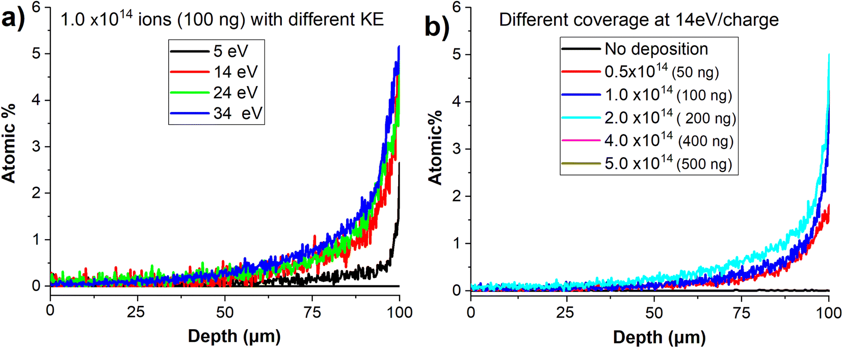 | ||
| Fig. 7 (a) EDX line scans along the depths of the VACNT substrates containing 1 × 10¹⁴ MoPOM anions deposited with different KE, (b) EDX line scans along the depths of the VACNT substrates at different coverages of MoPOM. | ||
We have also examined the dependence of the anion penetration depth into the VACNT material on ion coverage. The atomic percentage of Mo obtained from the cross-sectional EDX line scan analyses of the VACNTs is shown in Fig. 7b. We do not observe any substantial change in the penetration depth of MoPOM at the lower coverages of 0.5 × 10¹⁴, 1 × 10¹⁴ (100 ng), and 2 × 10¹⁴ (200 ng). However, at higher coverages of 4 × 10¹⁴ (400 ng) and 5 × 10¹⁴ (500 ng), the gradient of the atomic percentage of Mo along the VACNT becomes much shallower indicating that the anions penetrate deeper into the VACNT substrate reaching the 20–40 μm depth. We have previously demonstrated that a substantial fraction of soft-landed POM anions retain their charge on surfaces.52 This results in charge accumulation on a surface. The charged layer is stabilized by the image charge in the underlying surface.21,27 This generates a field gradient along the axis perpendicular to the surface. It is reasonable to assume that this field gradient promotes the migration of anions landed on the surface into the nanotubes and that the penetration of soft-landed anions into the VACNT substrate, which becomes more efficient as the electric field strength increases at higher anion coverages.
To confirm the reproducibility of the MoPOM anions penetration into the VACNT substrates, we performed soft landing of MoPOM with the coverage of 1 × 10¹⁴ ions and KE of 14 eV onto three different VACNT substrates and analyzed them using EDX. As seen in Fig. S11a,† all the samples show similar profiles for the penetration of MoPOM into the VACNT substrates. Soft landing MoPOM anions with the KE of 34 eV resulted in a similar penetration profile for MoPOM anions as shown in Fig. S11b.†
Mass spectrometry analysis of the VACNT/MoPOM prepared by soft landing MoPOM with the KE of 34 eV revealed the presence of the triply charged intact MoPOM (Fig. S7b†) as a dominant species on the surface. We also observed an abundant peak corresponding to the protonated doubly charged MoPOM. However, no peaks corresponding to fragment ions of MoPOM were observed in these experiments confirming deposition of intact anions on the surface.
In summary, a comparison of the distribution and depth penetration of soft-landed anions into vertical TiO2 NTs and VACNTs demonstrates that anions are distributed uniformly and penetrate efficiently into the conductive VACNT. Meanwhile, aggregation of anions on top of TiO2 NTs likely prevents their penetration into the semiconductive TiO2 NT.
Conclusion
In this study, we examined the distribution of soft-landed anions in both semiconductive and conductive 3D substrates using SEM and EDX analysis. We observed that soft-landed anions generate microaggregates on the semiconducting TiO2 NTs and only penetrate into the top 1.5 μm of both the 10 μm- and 6 μm-long TiO2 NTs. Meanwhile anions are uniformly distributed on the surface of 300 μm-long conductive VACNTs and penetrate into the top 40 μm of this substrate. Our results indicate that soft landed anions have different distributions in semiconductive and conductive substrates, which may be attributed to different substrate conductivity that affects the electric field generated by the anionic species in the 3D material. Particularly, EDX analysis revealed that the topmost 3.0 μm layer of the TiO2 NTs contains oxygen-rich titanium oxide species that are known for their lower electrical conductivity as compared to the stochiometric TiO2. This study demonstrates the feasibility of ion deposition into both conductive and semiconductive 3D nanostructures, providing valuable insights into the functionalization of porous structures using mass selected ions for potential applications in energy storage and electronics.Conflicts of interest
All authors declare that they have no conflicts of interest.Acknowledgements
The authors would like to thank Robert Seiler from the college of agriculture at Purdue University for his assistance with scanning electron microscopy analysis.References
- B. Ni, Y. Shi and X. Wang, Adv. Mater., 2018, 1802031, 1 Search PubMed.
- B. Ni and X. Wang, Chem. Sci., 2016, 3978 RSC.
- S. Proch, M. Wirth, H. S. White and S. L. Anderson, J. Am. Chem. Soc., 2013, 135, 3073 CrossRef CAS.
- S. Vajda, M. J. Pellin, J. P. Greeley, C. L. Marshall, L. A. Curtiss, G. A. Ballentine, J. W. Elam, S. Catillon-mucherie, P. C. Redfern, F. Mehmood and P. Zapol, Nat. Mater., 2009, 8, 213 CrossRef CAS.
- V. Prabhakaran, B. L. Mehdi, J. J. Ditto, M. H. Engelhard, B. Wang, K. D. D. Gunaratne, D. C. Johnson, N. D. Browning, G. E. Johnson and J. Laskin, Nat. Commun., 2016, 7, 1 Search PubMed.
- A. Rahman, R. Ak, T. Yamamoto and H. Kitagawa, J. Biosens. Bioelectron., 2016, 7, 1 Search PubMed.
- G. Kwon, G. A. Ferguson, C. J. Heard, E. C. Tyo, C. Yin, J. Debartolo, M. J. Pellin and S. Vajda, ACS Nano, 2013, 5808 CrossRef CAS.
- S. Vajda and M. G. White, ACS Catal., 2015, 5, 7152 CrossRef CAS.
- J. Lu, L. Cheng, K. C. Lau, E. Tyo, X. Luo, J. Wen, D. Miller, R. S. Assary, H. Wang, P. Redfern, H. Wu, J. Park, Y. Sun, S. Vajda, K. Amine and L. A. Curtiss, Nat. Commun., 2014, 5, 1 Search PubMed.
- E. C. Tyo and S. Vajda, Nat. Nanotechnol., 2015, 10, 577 CrossRef CAS.
- W. H. Woodward, M. M. Blake, Z. Luo, P. S. Weiss and A. W. Castleman, J. Phys. Chem. C, 2011, 115, 5373 CrossRef CAS.
- V. Franchetti, B. H. Solka, W. E. Baitinger, J. W. Amy and R. G. Cooks, Int. J. Mass Spectrom. Ion Phys., 1977, 23, 29 CrossRef CAS.
- A. K. Badu-tawiah, C. Wu and R. G. Cooks, Anal. Chem., 2011, 2648 CrossRef CAS.
- B. Gologan, J. R. Green, J. Alvarez, J. Laskin and R. G. Cooks, Phys. Chem. Chem. Phys., 2005, 7, 1490 RSC.
- P. Fremdling, T. K. Esser, B. Saha, A. A. Makarov, K. L. Fort, M. Reinhardt-Szyba, J. Gault and S. Rauschenbach, ACS Nano, 2022, 16, 14443 CrossRef CAS.
- K. Anggara, Y. Zhu, M. Delbianco, S. Rauschenbach, S. Abb and P. H. Seeberger, J. Am. Chem. Soc., 2020, 142, 21420 CrossRef CAS.
- J. Pelletier and A. Anders, IEEE Trans. Plasma Sci., 2005, 33, 1944 CAS.
- T. Film, D. Using and E. Ions, Materials, 2010, 3, 4109 CrossRef.
- J. Cyriac, T. Pradeep, H. Kang, R. Souda and R. G. Cooks, Chem. Rev., 2012, 112, 5356 CrossRef CAS.
- G. E. Johnson, D. Gunaratne and J. Laskin, Mass Spectrom. Rev., 2016, 35, 439 CrossRef CAS.
- J. Laskin, G. E. Johnson and J. Warneke, Angew. Chem., Int. Ed., 2018, 57, 16270 CrossRef CAS.
- A. Tata, C. Salvitti and F. Pepi, Int. J. Mass Spectrom., 2020, 450, 116309 CrossRef CAS.
- C. Salvitti, A. Troiani, F. Mazzei, C. D'Agostino, R. Zumpano, C. Baldacchini, A. R. Bizzarri, A. Tata and F. Pepi, Int. J. Mass Spectrom., 2021, 468, 116658 CrossRef CAS.
- A. Böttcher, P. Weis, A. Bihlmeier and M. M. Kappes, Phys. Chem. Chem. Phys., 2004, 6, 5213 RSC.
- E. T. Baxter, M. A. Ha, A. C. Cass, A. N. Alexandrova and S. L. Anderson, ACS Catal., 2017, 7, 3322 CrossRef CAS.
- G. E. Johnson, T. Priest and J. Laskin, ACS Nano, 2012, 6, 573 CrossRef CAS.
- J. Warneke, M. E. Mcbriarty, S. L. Riechers, M. H. Engelhard, E. Aprà, R. P. Young, N. M. Washton, C. Jenne, G. E. Johnson and J. Laskin, Nat. Commun., 2018, 9, 1 CrossRef CAS.
- P. Wang, O. Hadjar and J. Laskin, J. Am. Chem. Soc., 2007, 129, 8682 CrossRef CAS.
- J. Warneke, M. Mayer, M. Rohdenburg, X. Ma, J. K. Y. Liu and M. Grellmann, Proc. Natl. Acad. Sci., 2020, 117, 23374 CrossRef CAS.
- P. Weis, A. Bihlmeier, M. M. Kappes and U. Karlsruhe, Phys. Chem. Chem. Phys., 2004, 6, 5213 RSC.
- G. E. Johnson, Q. Hu and J. Laskin, Annu. Rev. Anal. Chem., 2011, 4, 83 CrossRef CAS.
- G. E. Johnson, R. Colby and M. Engelhard, Nanoscale, 2015, 7, 12379 RSC.
- V. Prabhakaran, B. Layla Mehdi, J. J. Ditto, M. H. Engelhard, B. Wang, K. D. D. Gunaratne, D. C. Johnson and N. D. Browning, Nat. Commun., 2016, 7, 1 Search PubMed.
- G. E. Johnson, V. Prabhakaran, N. D. Browning, B. L. Mehdi, J. Laskin, P. A. Kottke and A. G. Fedorov, Batteries Supercaps, 2018, 1, 97 CrossRef.
- P. Su, X. Chen, A. J. Smith, M. F. Espenship, H. Y. Samayoa Oviedo, S. M. Wilson, H. Gholipour-Ranjbar, C. Larriba-Andaluz and J. Laskin, Anal. Chem., 2021, 93, 11576 CrossRef CAS.
- D. R. Kirklin, L. J. S. Chickos and J. F. Liebman, Struct. Chem., 1996, 7, 335 CrossRef.
- V. Prabhakaran, J. Romo, A. Bhattarai, K. George, P. A. Kottke, A. G. Fedorov, P. Z. El-khoury, G. E. Johnson and J. Laskin, Chem. Commun., 2022, 58, 9060–9063 RSC.
- S. P. Albu, H. Tsuchiya, S. Fujimoto and P. Schmuki, Eur. J. Inorg. Chem., 2010, 4351 CrossRef CAS.
- V. A. Sadykov, S. N. Pavlova, N. F. Saputina, I. A. Zolotarskii, N. A. Pakhomov, E. M. Moroz, V. A. Kuzmin and A. V Kalinkin, Catal. Today, 2000, 61, 93 CrossRef CAS.
- R. E. Winans, S. Vajda, G. E. Ballentine, J. W. Elam and B. Lee, Top. Catal., 2006, 39, 145 CrossRef CAS.
- Z. Luo, W. Yang, A. Peng, Y. Zeng and J. Yao, Nanotechnology, 2009, 20, 345601 CrossRef.
- H. Wu, C. Yuan and Z. Luo, J. Mater. Chem. C, 2017, 5, 7561 RSC.
- S. M. Ali and M. A. M. Khan, Appl. Phys. A: Mater. Sci. Process., 2020, 126, 1 CrossRef.
- Y. Zhang, G. Zou, S. K. Doorn, H. Htoon, L. Stan, M. E. Hawley, C. J. Sheehan, Y. Zhu and Q. Jia, ACS Nano, 2009, 3, 2157 CrossRef CAS.
- P. Su, X. Chen, A. J. Smith, M. F. Espenship, H. Y. Samayoa Oviedo, S. M. Wilson, H. Gholipour-Ranjbar, C. Larriba-Andaluz and J. Laskin, Anal. Chem., 2021, 93, 11576 CrossRef CAS.
- S. Li, G. Zhang, D. Guo, L. Yu and W. Zhang, J. Phys. Chem. C, 2009, 113, 12759 CrossRef CAS.
- C. C. Chen, J. H. Chen, C. G. Chao and W. C. Say, J. Mater. Sci., 2005, 40, 4053 CrossRef CAS.
- S. Y. Kim, Y. K. Kim, I. S. Park, G. C. Jin, T. S. Bae and M. H. Lee, Appl. Surf. Sci., 2014, 321, 412 CrossRef CAS.
- R. Seemann, S. Herminghaus and K. Jacobs, Phys. Rev. Lett., 2001, 86, 5534 CrossRef CAS.
- F. Yang, Y. Hu, Q. Hu, S. Steiner, T. Frömling, L. Li, P. Wu, E. Pradal-Velázquez and D. C. Sinclair, J. Mater. Chem. A, 2022, 10, 891 RSC.
- B. Xu, H. Y. Sohn, Y. Mohassab and Y. Lan, RSC Adv., 2016, 6, 79706 RSC.
- K. D. D. Gunaratne, G. E. Johnson, A. Andersen, D. Du, W. Zhang, V. Prabhakaran, Y. Lin and J. Laskin, J. Phys. Chem. C, 2014, 118, 27611 CrossRef CAS.
Footnote |
| † Electronic supplementary information (ESI) available. See DOI: https://doi.org/10.1039/d2na00632d |
| This journal is © The Royal Society of Chemistry 2023 |