
 Open Access Article
 This Open Access Article is licensed under a Creative Commons Attribution-Non Commercial 3.0 Unported Licence
Electrical monitoring of organic crystal phase transition using MoS2 field effect transistor†
Ilan
Boulet
a,
Simon
Pascal
 a,
Frederic
Bedu
a,
Igor
Ozerov
a,
Alain
Ranguis
a,
Thomas
Leoni
a,
Conrad
Becker
a,
Laurence
Masson
a,
Aleksandar
Matkovic
b,
Christian
Teichert
b,
Olivier
Siri
a,
Claudio
Attaccalite
a,
Jean-Roch
Huntzinger
c,
Matthieu
Paillet
c,
Ahmed
Zahab
c and
Romain
Parret
*a
a,
Frederic
Bedu
a,
Igor
Ozerov
a,
Alain
Ranguis
a,
Thomas
Leoni
a,
Conrad
Becker
a,
Laurence
Masson
a,
Aleksandar
Matkovic
b,
Christian
Teichert
b,
Olivier
Siri
a,
Claudio
Attaccalite
a,
Jean-Roch
Huntzinger
c,
Matthieu
Paillet
c,
Ahmed
Zahab
c and
Romain
Parret
*a
aAix Marseille Université, CNRS, CINAM, UMR 7325, Campus de Luminy, 13288, Marseille, France. E-mail: romain.parret@.univ-amu.fr; Tel: +33 6 62922867
bInstitute of Physics, Montanuniversität Leoben, 8700, Leoben, Austria
cLaboratoire Charles Coulomb, UMR 221, Univ. Montpellier, CNRS, Montpellier, France
First published on 14th February 2023
Abstract
Hybrid van der Waals heterostructures made of 2D materials and organic molecules exploit the high sensitivity of 2D materials to all interfacial modifications and the inherent versatility of the organic compounds. In this study, we are interested in the quinoidal zwitterion/MoS2 hybrid system in which organic crystals are grown by epitaxy on the MoS2 surface and reorganize in another polymorph after thermal annealing. By means of field-effect transistor measurements recorded in situ all along the process, atomic force microscopy and density functional theory calculations we demonstrate that the charge transfer between quinoidal zwitterions and MoS2 strongly depends on the conformation of the molecular film. Remarkably, both the field effect mobility and the current modulation depth of the transistors remain unchanged which opens up promising prospects for efficient devices based on this hybrid system. We also show that MoS2 transistors enable fast and accurate detection of structural modifications that occur during phases transitions of the organic layer. This work highlights that MoS2 transistors are remarkable tools for on-chip detection of molecular events occurring at the nanoscale, which paves the way for the investigation of other dynamical systems.
Introduction
Two dimensional (2D) transition metal dichalcogenides (TMDC) are considered promising materials for nanoelectronic applications due to their mechanical properties to meet flexible requirements, scalability in terms of thickness to take advantage of their unique optical properties such as direct band gap inducing high efficiency luminescence, their high specific surface area and high chemical sensitivity for compact and efficient sensors.1–7 Many effects, induced by the adsorption of organic molecules on top of field effect transistor (FET) based on 2D materials have recently been demonstrated. Among the most striking effects, benzyl viologen adsorption or pyrimidine reduces the contact resistance that often limits the performance of TMDC-based devices.8,9 Thiol functionalized molecules can repair defects such as sulphur vacancies hosted in MoS2 while inducing either n- or p-type doping.10 Comparative studies with different molecules have shown that a wide range of doping can be induced by the creation of organic/2D materials hybrid heterostructures. Either n- or p-type doping and even quasi-metallic states can be achieved.10–34 Among organic molecules, quinoidal zwitterions (QZ) are particularly interesting because they can act as efficient dopants and their epitaxial growth on van der Waals materials in the sub-monolayer regime has been reported.35,36 In addition, QZs are simple chemical building blocks that can be very widely modified by molecular engineering to tune optical properties, size, supramolecular interactions, electrostatic or magnetic properties in their coordination complexes.36–43In this work, we will show that on crystalline MoS2 surfaces, QZs crystallize following epitaxy-guided growth. This type of growth guarantees good interface quality allowing, in particular, efficient charge transfers. The resulting layer, formed of microcrystals, induces n-type doping of MoS2. Subsequent thermal annealing realized on grown QZ layer lead to new molecular conformations accompanied by strong modifications of the current flowing in the transistors. Based on the analysis of FET characteristics, atomic force microscopy (AFM) and density functional theory (DFT) calculations, our study reveals that the charge transfers that occur at the organic/MoS2 interface are highly dependent on the molecular conformation. Such results show the usefulness of MoS2-based sensors to probe events occurring at the nanoscale, such as molecular growth and conformational changes.
Results and discussion
Fig. 1a shows a schematic representation of the studied hybrid materials. The growth starts with the evaporation of a powder of QZ–C4, which is a quinoidal zwitterion with n-butyl substituents (R = C4H9) shown in Fig. 1b. The organic crystal epitaxial growth is realized by condensation of the QZ–C4 vapour on top of MoS2 transistors. Fig. 1b presents the band diagram alignment of MoS2 and QZ–C4, indicating that an electron transfer from the QZ–C4 toward the MoS2 is expected.41,44 This transfer is confirmed by ab initio calculations (see ESI†). Fig. 1c shows typical optical micrographs of both the MoS2 transistors (the fabrication process is detailed in the experimental method part) and the QZ–C4 powder which is composed of micrometric crystals exhibiting a flat geometry. In powder form, the QZ–C4 molecules, which hosts a strong permanent electrostatic dipole, crystallizes as head-to-tail dimers via intermolecular hydrogen bonding interaction.41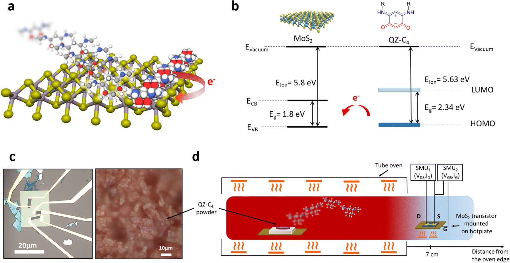 | ||
| Fig. 1 (a) Scheme of the studied hybrid materials, where organic crystals of QZ–C4 grow by epitaxy on MoS2. (b) Band diagram of MoS2 (left)44 and QZ–C4 (right) determined by cyclic voltammetry measurements.41 An increase of the MoS2 electron density is expected in the hybrid materials through charge transfer from the QZ–C4. (c) Optical images of the MoS2 transistors (left) and of the QZ–C4 powder (right). (d) Scheme of the molecular doping reactor. The colour in the tube illustrates the temperature distribution during the QZ–C4 evaporation: 130 °C inside the oven (red) and about room temperature in the right side of the tube that stands out of the oven (light blue). The studied transistors are positioned at 7 cm from the oven edge. The electrical measurements are performed using two source measure units (SMU). | ||
The evaporator of molecules used in this work consists in a glass tube that can be pumped under a high vacuum of 10−7 mbar (Fig. 1d). This tube is embedded is a tubular oven used to heat both the molecules initially placed in a copper crucible on the left side and the tube walls to avoid molecular adsorption. The molecular flow is directed toward the edges of the oven where the MoS2 transistor is placed (at a distance of 7 cm away from the edge of the oven) and maintained at room temperature. The MoS2 transistor is mounted on a homemade sample holder equipped with a heating resistor and a Pt100 temperature sensor. The sample can thus be heated independently, allowing thermal annealing processes both before and after the adsorption of molecules. The transistor is connected to source measure units (SMU in Fig. 1d) using electrical feedthroughs, allowing in situ electrical measurements.
Before molecule evaporation, the MoS2 transistor is thermally annealed in situ at 120 °C for 1 hour. This temperature is the optimal trade-off to improve both the sample performance and its surface cleanliness while avoiding the desulfurization of MoS2 which can induce a metallic transition and strongly modify the transistor behaviour.10 During this first step, the drain-source current unambiguously increases. This well-known effect is mainly due to the desorption of O2/H2O and the improvement of the metal–MoS2 contact interface.45 Thus, after this important preliminary step, the MoS2 surface is left as clean as possible to promote the formation of molecular layers of optimal interfacial quality (see ESI†).
After this preparation step, the QZ–C4 powder is heated up to its sublimation temperature (TS = 130 °C) and the deposition of the QZ–C4 molecules occurs on the MoS2, which is maintained at room temperature. The QZ–C4 deposition is carried out in two steps and is monitored in situ by measuring drain-source current of the MoS2 device, while a drain-source voltage (VDS = 1 V) and zero gate voltage (VGS = 0 V) are applied to the transistors terminals as shown in Fig. 2. The first step lasts 3500 s [0–3500 s]. At 3500 s, the oven is opened for 300 s to visually check the sample appearance and to record a transfer characteristic while the condensation of QZ–C4 is interrupted. Then a second evaporation step is carried out until a visible molecular layer forms on the surface of the sample [3800–6000 s]. Far from being monotonous, the evolution of the current throughout the whole process presents many variations including both increases and decreases (Fig. 2). The drain source current evolution of the two samples shown in Fig. 2 are rather comparable as they share most of the current variations. Similar trends are observed on all the investigated samples whatever the MoS2 thickness. The growth of the thick molecular layer is always accompanied by an obvious increase of the drain source current and subtler variations that will be discussed later. The reproducibility of the experiment has also been checked with two other identical samples based on four layers thick MoS2.
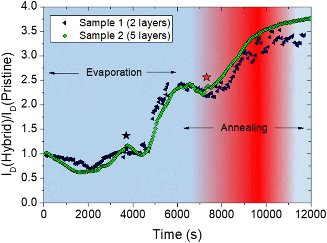 | ||
| Fig. 2 Evolution of the drain-source current ratio ID (hybrid)/ID (pristine) as a function of time during 1/evaporation–condensation of the QZ–C4 and 2/post-deposition thermal annealing of sample 1 (blue triangle symbols) and sample 2 (green diamond symbols) as labelled on the graph. VDS = 1 V, VGS = 0 V, ID (pristine) is 1 μA for sample 1 and 0.2 μA for sample 2. The MoS2 thicknesses are two layers for sample 1 and five layers for sample 2. The blue-red-blue background illustrates the transistor sample temperature evolution during the deposition/post-annealing process. Light blue corresponds to room temperature and full red corresponds to 110 °C. The black star indicates the time when the oven was opened to visually check the appearance of the sample and to record a transfer characteristic. The red star indicates the time when the post annealing temperature is 70 °C. | ||
In a third step, still followed in situ, the molecular flow is interrupted by switching off the oven heater and we carried out a post-deposition thermal annealing of the device up to 110 °C. The annealing temperature is set 20 °C below the evaporation temperature of the QZ–C4 in order to avoid any degradation of the molecules. When the temperature reaches 70 °C we observe by naked eye the appearance of interference fringes on the sample surface accompanied by an increase in chamber pressure (see ESI†). These effects indicate a decrease in the thickness of the molecular layer and its partial evaporation. This evolution continues up to a temperature of 110 °C at which the sample regains its initial appearance. The evolution of the current is, once again, complex and will be discussed later. We should note that the current increases significantly again during this step. Overall and considering the whole deposition/post-annealing process, the current increased by a factor 3–4 for both samples (Fig. 2).
To analyse the morphology of the molecular layers, we performed AFM imaging ex situ at room temperature after the deposition process (Fig. 3a) and after the post-annealing step (Fig. 3d and e). The deposition process leads to the formation of a thick layer of QZ–C4 microcrystals exhibiting an elongated and flattened shape. Six preferred growth directions are observed, split into three chiral pairs with 60° periodicity, and 23.5° ± 0.8° split between the chiral pair directions. The growth directions clearly indicate epitaxy of the QZ crystals on MoS2 as the motif follows the trigonal symmetry of the substrate (Fig. 3c). This type of growth guarantees high interface quality allowing, in particular, efficient charge transfers as discussed in the following. To get into detail, we carefully analysed the geometry of organic layer. Fig. 3b presents a topographic profile taken on the Fig. 3a. We extracted an average thickness of about 70 nm. Considering the AFM image, it appears that the variations around this average value are due to the inclination of the microcrystals with respect to the surface (see ESI†). We thus determined the geometry of the crystal by performing a statistical analysis leading to an average set of dimensions (length = 1.5 ± 0.1 μm, width = 60 ± 10 nm and thickness = 20 ± 5 nm). After the post-annealing at 110 °C, most of the molecules from the microcrystals have re-evaporated from the MoS2 surface leaving a thin compact layer of round aggregates with an average thickness of about 3 nm (Fig. 3d–f).
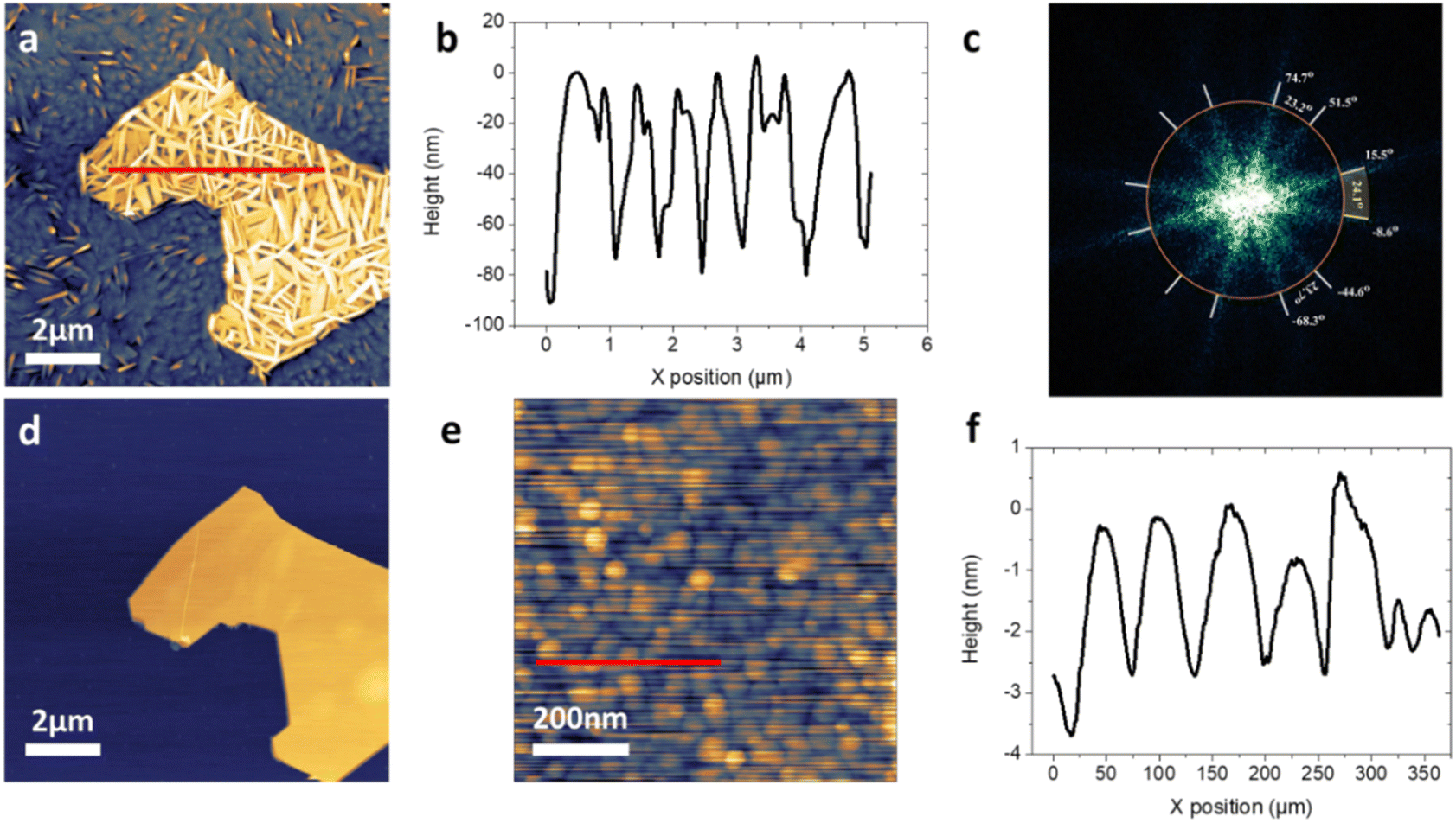 | ||
| Fig. 3 (a) AFM topography image of the condensed phase. (b) Extracted height profile from (a) (red line). (c) 2D fast Fourier transform (2D-FFT) carried out by cropping a binary mask from the crystallites selectively only on the MoS2 flake. The orange circle is 20 μm−1 in diameter. The procedure used to perform the FFT has been described.46 We carefully checked that the flake edges play a negligible role in the observed FFT pattern (d) AFM topography image of the post-annealed phase. (e) High-resolution AFM topography image of the post-annealed phase. (f) Extracted height profile from (e) (red line). | ||
To investigate the effect of the molecular morphologies on the behaviour of MoS2 transistors, the transfer characteristics were recorded and compared to those of bare pristine MoS2. In Fig. 4a and b, we present the transfer characteristics of the sample 1 (two layers of MoS2) recorded at VDS = 1 V: (1) after the initial in situ thermal annealing, (2) after the first QZ–C4 deposition (which corresponds to 3500 s in Fig. 2), (3) after a second QZ–C4 deposition (which corresponds to 6000 s in Fig. 2), and (4) after the post-deposition thermal annealing. Apart from a shift of the threshold voltage that increases in absolute value at each stage, most features of transfer characteristics are preserved. The ION/IOFF ratio remains large, about six orders of magnitude. The sub-threshold slope is not affected by the presence of the organic layers which indicates that the current flows only through the MoS2 channel of the transistor.
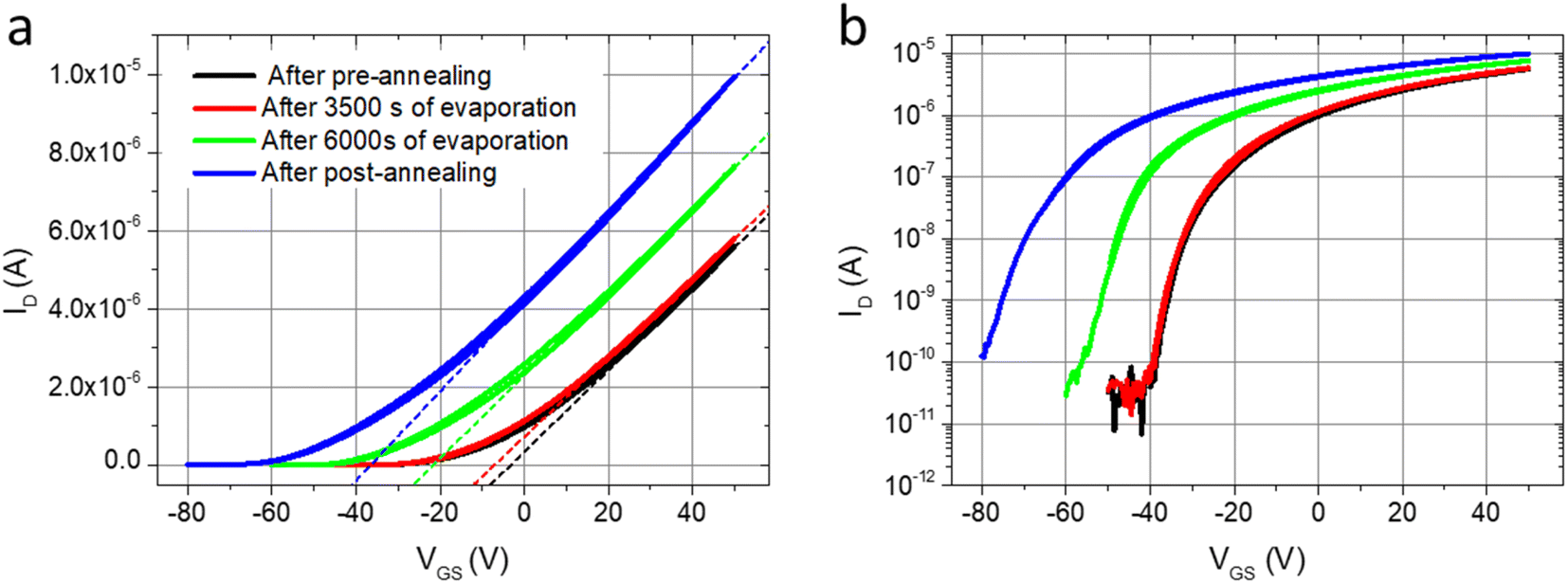 | ||
| Fig. 4 (a) Transfer characteristic recorded at VDS = 1 V of the device annealed in situ (black), after the first molecular deposition (red), after the second molecular deposition (green) and after the post-annealing (blue). Both gate voltage sweep directions are plotted, which shows negligible hysteresis. (b) Same transfer characteristics presented in semi-log scale. | ||
By analysing these FET measurements, we calculated the field effect mobility and the carriers density (see Methods). We find that the field effect mobility remains almost unchanged at the value of μ = 10 ± 1 cm2 V−1 s−1. The carriers densities calculation is based on the determination of the threshold voltage which shifts toward negative values, indicating electron transfer from the molecules toward the MoS2. We obtain, with respect to the pristine MoS2 transistor ΔVth = −3.85 V (Δn = 2.8 × 1011 cm−2) after the first deposition, ΔVth = −18.4 V (Δn = 1.3 × 1012 cm−2) after the second deposition and ΔVth = −33.3 V (Δn = 2.4 × 1012 cm−2) after the post-deposition annealing.
To understand these induced doping levels, we performed DFT calculations in order to determine molecular states positions with respect to the MoS2 band structure, binding energy of the QZ–C4 molecules to the MoS2 surface (see ESI†) and charge transfer between the molecules and MoS2. We considered two cases in the simulation: the case of a single QZ–C4 molecule deposited on MoS2 surface and the case of two molecules in the head-to-tail configuration. We found that a single molecule transfers 0.0183 electron to the surface. In the case of two molecules in head-to-tail configuration, the transferred charge is 0.00786 electron. Considering a compact layer of dimers formed by two molecules in head-to-tail configuration, and the 0.00786 electron transferred by dimers, we get an induced electron density of about 1012 cm−2 into the MoS2 in agreement with the experimental results.
In Fig. 5, we present the experimental data on (a) induced doping and (b) the field-effect mobilities of six samples with different MoS2 thicknesses 1L, 2L, 4L, 4L, 5L and 8L as a function of the post-deposition annealing temperature. The thickness nL corresponds to the number of n monolayers in the MoS2 flake used to fabricate the device. The values of induced doping and mobilities at T = 25 °C (RT) correspond to the as-deposited phase (not annealed). These devices had field-effect mobilities in the range of 0.3–35 cm2 V−1 s−1, which is in a good agreement with the data reported for exfoliated MoS2 on SiO2 substrates.45 All these devices behave the same way under the effect of QZ–C4 adsorption, crystallisation, and thermally-induced changes in the molecular film conformation. The mobility remains unchanged for most samples, and even increases by two for two samples (Fig. 5b). These results unambiguously show that the molecular layers, either as-deposited or annealed, can dope the MoS2 layer without degrading the field effect mobility. In Fig. 5a, we show that the induced doping increases when the number of layers decreases. These results show that the thinner the MoS2, the more sensitive is the transistor.
 | ||
| Fig. 5 Annealing temperature dependence of the induced doping (a) and the field effect mobility (b) measured on six samples of MoS2 thicknesses 1L, 2L, 4L, 4L, 5L and 8L. | ||
In order to interpret the multiple changes observed, we now examine in more details the evolution of the drain source current as a function of time presented in Fig. 2. Given the reproducibility of these variations, it seems reasonable to infer that they are correlated with key stages of QZ–C4 crystal growth. Thus, in order to image the different stages of the growth of organic crystals, we performed a deposition of QZ–C4 on MoS2 flakes placed at several distances from the edge of the oven. Given the condensation of the molecules on the samples and on the cold walls of the tube, the molecular flux decreases with this distance. This allows obtaining different QZ–C4 concentrations on different flakes of MoS2 in a single experiment. The different QZ–C4 phases obtained by this way are then imaged by AFM (Fig. 6). The measurement of the temperature at the different positions of the tube outside the oven showed that the temperature was constant and equal to room temperature above 6.5 cm with less than 2 °C variations (see ESI†). Thus, the QZ–C4 concentration is the only varying parameter for the QZ–C4 phases corresponding to images of Fig. 6a–h. In the early deposition stages (low QZ–C4 concentration, Fig. 6a–c), the deposit is essentially composed of round nanoparticles and few larger islands of variable shapes. As the QZ–C4 concentration increases, the QZ–C4 islands coalesce and get larger and larger. Such a liquid-like behaviour reflects a certain disorder of the organic layer structure. These growing stages match the drop in the drain-source current of the MoS2 transistors observed around 2000 s of deposition (Fig. 2). Transfer characteristics recorded around the same deposition time exhibit a reduced slope in the transistor's ON-state signalling a reduction of the field effect mobility (see ESI†). We thus observe a strong correlation between the presence of the disordered organic phase and the reduction of the field effect mobility that would explain the current drop observed around 2000 s of deposition. In Fig. 6d–h, QZ–C4 needle-like crystallites begin to form in the largest islands indicating that crystallization needs a critical concentration to be initiated. Then, the number of crystallites increases with the QZ–C4 concentration (and thus with the deposition duration) until the entire surface is covered (Fig. 6h). The structure of the organic layer tends towards an increasing order until forming the well-ordered epitaxial structure presented in Fig. 3a. These growth stages are correlated with an increase of the current. The transfer characteristic also presents obvious changes: an increase of the slope in the ON-state of the transistor and a shift of the threshold voltage indicating respectively an increase of the field effect mobility and an increase of the electron density. The field effect mobility evolution is correlated with the progressive organization of the organic layer while the increase of the electron density originates from electron transfer from the QZ–C4 crystals toward the MoS2.
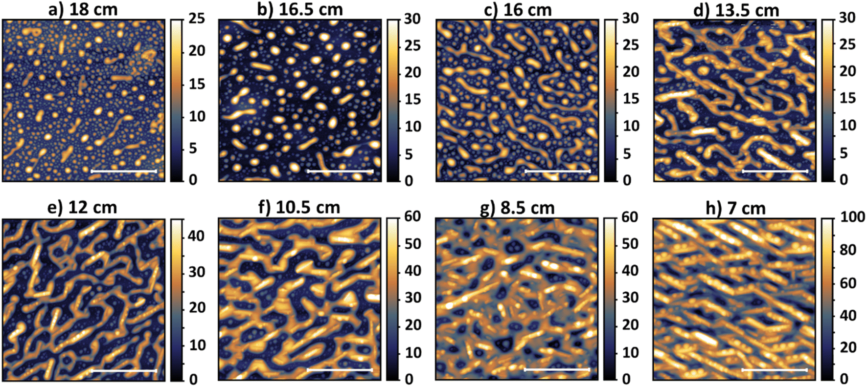 | ||
| Fig. 6 (a–h) AFM images of the organic phases located at different distances from the edge of the oven (see Fig. 1d scheme). Vapour concentration is increasing from (a)–(h). All the transport measurements shown in other figures have been performed with sample positioned at 7 cm (h). Scale bars are 2 μm for every image and height scale are in nm. | ||
During the acquisitions shown in Fig. 2, after 3500 s of deposition, the oven has been opened for a few minutes, inducing a short interruption of the QZ–C4 deposition necessary to visually check the sample appearance and to record a transfer characteristic with an interrupted molecular flow. As the flow resumes, the current initially decreases slightly over 1000 s and then increases largely up to a factor of 2.5 compared to the pristine sample. Such evolution could not be attributed to the interruption of molecular flow since uninterrupted experiments exhibit similar evolution (see ESI†). An interpretation, which could explain this evolution, is that a molecular layer presenting a good organization is reached at 3500 s and that the addition of molecules on top of this layer could be accompanied by a molecular reorganization that tends to induce disorder at the beginning and to evolve towards an orderly phase afterwards. Using the same arguments as before, the current decrease and increase indicate a further degradation and recovery of field effect mobility correlated with the degree of disorder of the organic phase.
During the post-deposition annealing phase, a similar evolution of the current is observed. It first decreases until the sample temperature reaches 70 °C and then increases again significantly. Below 70 °C, the sample appearance does not change, indicating that the QZ–C4 quantity remains constant on the sample. The MoS2 carriers density is thus not expected to be modified. On the contrary, it is highly probable that the molecular phase becomes disordered under the effect of thermal agitation. Based on this assumption, the drop in drain-source current is again most likely due to a field effect mobility degradation. At 70 °C, interference fringes visible by the naked eye appear on the surface of the sample indicating a reduction in the thickness of the organic layer, which is due to the re-evaporation of QZ–C4. The morphology of the organic layer is then profoundly modified as the microcrystals disappear leaving an inhomogeneous layer. During these modifications of the organic layer, the transfer characteristics of transistors become unstable with the appearance of a large hysteresis (see ESI†). When the annealing temperature is increased beyond 70 °C, we observe that both the morphological inhomogeneity of the organic layer and the instabilities of the electrical response of the transistors are progressively reduced. The annealing temperature at 110 °C is the best trade-off allowing an optimization of the structure of the organic layer from which derives optimal electrical properties including in particular a field effect mobility comparable to that of pristine MoS2 and a strong n-type doping (Fig. 5).
To explain the conformational change of the organic layer induced by a post-annealing at 110 °C, namely the formation of the flattened round aggregates, we first notice that such aggregates are observed in the early stage deposition then they disappear in favour of microcrystals when the QZ–C4 concentration exceeds a certain critical concentration (Fig. 6a–d). We thus compared the volume of the organic layer after the post-deposition annealing to the volume occupied by the molecules at different stages of the growth. It appears that the volume of molecules is lower in the annealed phase than in the transient phase where the first elongated crystals appear (Fig. 6d). Given that the molecular concentration is lower than the critical concentration mentioned above, QZ–C4 form spherical aggregates, which is the stable conformation at these low molecular concentrations. No specific organization of the aggregates was observed on the surface. Presumably, the high polydispersity in size of the aggregates does not allow for a good epitaxy with the MoS2 surface to be maintained (see ESI†). It is important to note that the post-annealing is a top-down process which allows the formation of dense layer of aggregates that we never got by our bottom-up approach. Indeed, during the QZ–C4 deposition the microcrystals appear before the completion of a molecular layer. In the as-deposited layer the very anisotropic geometry of the microcrystals limits the surface of the molecules in contact with the MoS2 because of steric hindrance. On the contrary, and this is presumably the reason why the induced doping is the highest, the organic layer obtained after the post-deposition annealing exhibits a high surface density, which makes it possible to have a large effective surface of the QZ–C4/MoS2 interface.
Finally, combining studies of the organic layer morphologies with quantitative measurements of the doping and the field effect mobility provide a comprehensive interpretation of the drain-source current evolution during the entire process.
Conclusions
In summary, we have investigated the electrical response of MoS2-FET during the growth of quinoidal zwitterion crystals on the MoS2 surface and during subsequently carried out thermal annealing. We have shown that the charge transfers occurring at the QZ–C4/MoS2 interface are strongly dependent on the molecular film conformation. Interestingly, the MoS2 FET retain all the other performance indicators such as field effect mobility and current modulation depth. These results highlight the compatibility of QZs with MoS2 and open interesting perspectives for future devices insofar as QZs can be widely modified by chemical engineering to induce specific functions required in applications such as optoelectronics or sensors. We also showed that MoS2 transistors could dynamically detect molecular organisation changes that occur during the growth of organic crystals and conformational changes induced by thermal annealing. This result highlights the relevance of MoS2 transistors for on-chip detection of molecular events occurring at the nanoscale, which paves the way for the investigation of other dynamical systems.Methods
MoS2 transistor fabrication
MoS2 flakes are obtained by micromechanical cleavage of a MoS2 crystal (HQ graphene) using scotch tape (Nitto) and PDMS slabs (Gel-Pak). The flakes are transferred onto 90 nm or 300 nm thick dry-oxidized SiO2 layers grown on a heavily doped p-type Si substrate. Flakes are selected by optical microscopy and their thicknesses are determined by optical contrast. They are then patterned in a rectangular shape by e-beam lithography (Pioneer Raith) and reactive ion etching in SF6 gas (Plassys). Finally, the electrodes (Cr/Au) on top of the MoS2 flakes and the contact pads are patterned by e-beam lithography followed by metal evaporation and lift-off.Quinoidal zwitterion synthesis
The compound QZ–C4 was synthesized in two steps from commercial 4,6-diaminoresorcinol dihydrochloride following a reported procedure.41 After a transamination reaction in presence of excess n-butylamine, a straightforward purification by precipitation afforded QZ–C4 in high yield as an orange-pink powder.Doping reactor
Organic films were grown using a doping reactor made with a glass tube, which can be pumped under a high vacuum (10−7 mbar) and a tube oven to heat the molecules and the tube walls. The oven can be opened at any time without breaking the vacuum in the tube, which allows both to inspect the sample and to cool the tube more quickly in order to interrupt the flow of molecules. Electrical connections to the sample holder allow in situ electrical measurements and independent heating of the sample. Sample preparation (pre-annealing), organic layer growth and post-annealing were carried out under high vacuum (base pressure of 10−7 mbar). The electrical powers applied to the heating sample holder have been calibrated to maintain the annealing temperatures constant without regulation thanks to the thermal losses of the setup.Electrical measurements
Electrical measurements were carried out in situ using an Agilent 1500a SourceMeter. Voltage sources were used to apply VDS voltage between source and drain electrodes and VGS voltage between gate and source electrodes. ID drain current and IG gate current were measured. Transfer curves were acquired with ΔVGS = 0.5 V voltage steps and time step of 200 ms. All these measurements were repeated several times to ensure their reproducibility.FET measurements analysis
We calculated the field effect mobility at the voltage threshold (Vth, extracted by finding the interception of the tangential line of the linear region of the transfer characteristic and the X-axis) using eqn (1):45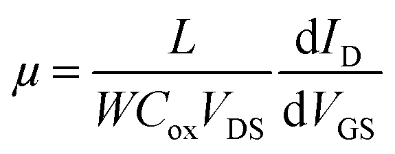 | (1) |
 | (2) |
Atomic force microscopy
AFM images were recorded using a XE-100 (Park Systems) equipped with a 100 × 100 × 12 μm scanner in tapping mode at room temperature. Silicon probes HQ:NSC15/AL BS, Mikromasch with curvature radius of about 8 nm (supplier specifications). The AFM images were analyzed using the Gwyddion software.47Computational details
We simulated the QZ molecules adsorbed on MoS2 using 8 × 8 × 1 supercell. The total energy and the atomic position were obtained using DFT with PBE-sol functional48 plus van der Waals corrections.49 We used a cutoff of 90 Ry for the wave function, a gamma point sampling for the k-points, and a distance of 41 (a.u.) in the z-direction in order to reduce the interaction between the replica. We verified that increasing the sampling of the Brillouin zone to 2 × 2 × 1 does not change the structural properties. Calculations were performed using Quantum-Espresso (QE) code.50 The atomic positions were then optimized using the conjugate gradient algorithm implemented in QE code. Charge transfer between the molecule and the surface is calculated using the Bader approach.51Data availability
The datasets generated and/or analysed during the current study that are not included in this published article (and its ESI files†) are available from the corresponding author on reasonable request.Author contributions
This manuscript was written through contributions of all authors. All authors have given approval to the final version of the manuscript.Conflicts of interest
There are no conflicts to declare.Acknowledgements
This work has been supported by the Agence Nationale de la Recherche (ANR) through grant (ANR-20-CE24-0006), the Centre for International Cooperation & Mobility (ICM) of the Austrian Agency for International Cooperation in Education and Research (OeAD-GmbH) under project FR 12/2019. O. S. thanks the Ministère des Affaires étrangères for the PHC Amadeus Program Exchange. Nanofabrication processes were performed in PLANETE cleanroom facility (CINaM, Marseille). C. A. acknowledges A. Saul and K. Boukari for the management of the computer cluster Rosa, and T. Ammouli for the help in the charge transfer calculations. R. P. acknowledges T. Michel for the help in Raman spectroscopy measurements.References
- D. J. Late, Y.-K. Huang, B. Liu, J. Acharya, S. N. Shirodkar, J. Luo, A. Yan, D. Charles, U. V. Waghmare, V. P. Dravid and C. N. R. Rao, Sensing Behavior of Atomically Thin-Layered MoS2 Transistors, ACS Nano, 2013, 7(6), 4879–4891, DOI:10.1021/nn400026u.
- X. Zhang, J. Grajal, J. L. Vazquez-Roy, U. Radhakrishna, X. Wang, W. Chern, L. Zhou, Y. Lin, P.-C. Shen, X. Ji, X. Ling, A. Zubair, Y. Zhang, H. Wang, M. Dubey, J. Kong, M. Dresselhaus and T. Palacios, Two-Dimensional MoS2-Enabled Flexible Rectenna for Wi-Fi-Band Wireless Energy Harvesting, Nature, 2019, 566(7744), 368–372, DOI:10.1038/s41586-019-0892-1.
- N. Li, Q. Wang, C. Shen, Z. Wei, H. Yu, J. Zhao, X. Lu, G. Wang, C. He, L. Xie, J. Zhu, L. Du, R. Yang, D. Shi and G. Zhang, Large-Scale Flexible and Transparent Electronics Based on Monolayer Molybdenum Disulfide Field-Effect Transistors, Nat. Electron., 2020, 3(11), 711–717, DOI:10.1038/s41928-020-00475-8.
- O. Lopez-Sanchez, D. Lembke, M. Kayci, A. Radenovic and A. Kis, Ultrasensitive Photodetectors Based on Monolayer MoS2, Nat. Nanotechnol., 2013, 8(7), 497–501, DOI:10.1038/nnano.2013.100.
- D. Krasnozhon, D. Lembke, C. Nyffeler, Y. Leblebici and A. Kis, MoS2 Transistors Operating at Gigahertz Frequencies, Nano Lett., 2014, 14(10), 5905–5911, DOI:10.1021/nl5028638.
- M. S. Fuhrer and J. Hone, Measurement of Mobility in Dual-Gated MoS2 Transistors, Nat. Nanotechnol., 2013, 8(3), 146–147, DOI:10.1038/nnano.2013.30.
- B. Radisavljevic, A. Radenovic, J. Brivio, V. Giacometti and A. Kis, Single-Layer MoS2 Transistors, Nat. Nanotechnol., 2011, 6(3), 147–150, DOI:10.1038/nnano.2010.279.
- D. Kiriya, M. Tosun, P. Zhao, J. S. Kang and A. Javey, Air-Stable Surface Charge Transfer Doping of MoS2 by Benzyl Viologen, J. Am. Chem. Soc., 2014, 136(22), 7853–7856, DOI:10.1021/ja5033327.
- A. Matković, A. Petritz, G. Schider, M. Krammer, M. Kratzer, E. Karner-Petritz, A. Fian, H. Gold, M. Gärtner, A. Terfort, C. Teichert, E. Zojer, K. Zojer and B. Stadlober, Interfacial Band Engineering of MoS2/Gold Interfaces Using Pyrimidine-Containing Self-Assembled Monolayers: Toward Contact-Resistance-Free Bottom-Contacts, Adv. Electron. Mater., 2020, 6(5), 2000110, DOI:10.1002/aelm.202000110.
- D. M. Sim, M. Kim, S. Yim, M.-J. Choi, J. Choi, S. Yoo and Y. S. Jung, Controlled Doping of Vacancy-Containing Few-Layer MoS 2via Highly Stable Thiol-Based Molecular Chemisorption, ACS Nano, 2015, 9(12), 12115–12123, DOI:10.1021/acsnano.5b05173.
- M. Morant-Giner, J. M. Carbonell-Vilar, M. Viciano-Chumillas, A. Forment-Aliaga, J. Cano and E. Coronado, Functionalisation of MoS2 2D Layers with Diarylethene Molecules, J. Mater. Chem. C, 2021, 9(33), 10975–10984, 10.1039/D1TC01133B.
- Y. Zhao, S. Bertolazzi, M. S. Maglione, C. Rovira, M. Mas-Torrent and P. Samorì, Molecular Approach to Electrochemically Switchable Monolayer MoS2 Transistors, Adv. Mater., 2020, 32(19), 2000740, DOI:10.1002/adma.202000740.
- A. R. Brill, E. Koren and G. de Ruiter, Molecular Functionalization of 2D Materials: From Atomically Planar 2D Architectures to off-Plane 3D Functional Materials, J. Mater. Chem. C, 2021, 9(35), 11569–11587, 10.1039/D1TC01534F.
- B. Ryu, H. Nam, B.-R. Oh, Y. Song, P. Chen, Y. Park, W. Wan, K. Kurabayashi and X. Liang, Cyclewise Operation of Printed MoS2 Transistor Biosensors for Rapid Biomolecule Quantification at Femtomolar Levels, ACS Sens., 2017, 2(2), 274–281, DOI:10.1021/acssensors.6b00795.
- J. Zhao, N. Li, H. Yu, Z. Wei, M. Liao, P. Chen, S. Wang, D. Shi, Q. Sun and G. Zhang, Highly Sensitive MoS2 Humidity Sensors Array for Noncontact Sensation, Adv. Mater., 2017, 29(34), 1702076, DOI:10.1002/adma.201702076.
- R. Tripathi and A. Misra, A Novel Approach towards Molecular Memory Device in Gate Tunable Structure of MoS2-Graphene, Nano Res., 2021, 14(1), 177–184, DOI:10.1007/s12274-020-3063-7.
- M. I. Alam, T. Takaoka, H. Waizumi, Y. Tanaka, M. S. Al Mamun, A. Ando and T. Komeda, Sensor Behavior of MoS2 Field-Effect Transistor with Light Injection toward Chemical Recognition, RSC Adv., 2021, 11(43), 26509–26515, 10.1039/D1RA03698J.
- D.-W. Lee, J. Lee, I. Y. Sohn, B.-Y. Kim, Y. M. Son, H. Bark, J. Jung, M. Choi, T. H. Kim, C. Lee and N.-E. Lee, Field-Effect Transistor with a Chemically Synthesized MoS2 Sensing Channel for Label-Free and Highly Sensitive Electrical Detection of DNA Hybridization, Nano Res., 2015, 8(7), 2340–2350, DOI:10.1007/s12274-015-0744-8.
- H. Nam, B.-R. Oh, P. Chen, M. Chen, S. Wi, W. Wan, K. Kurabayashi and X. Liang, Multiple MoS2 Transistors for Sensing Molecule Interaction Kinetics, Sci. Rep., 2015, 5(1), 10546, DOI:10.1038/srep10546.
- D. Sarkar, W. Liu, X. Xie, A. C. Anselmo, S. Mitragotri and K. Banerjee, MoS2 Field-Effect Transistor for Next-Generation Label-Free Biosensors, ACS Nano, 2014, 8(4), 3992–4003, DOI:10.1021/nn5009148.
- N. T. Trung, M. I. Hossain, M. I. Alam, A. Ando, O. Kitakami, N. Kikuchi, T. Takaoka, Y. Sainoo, R. Arafune and T. Komeda, In Situ Study of Molecular Doping of Chlorine on MoS2 Field Effect Transistor Device in Ultrahigh Vacuum Conditions, ACS Omega, 2020, 5(43), 28108–28115, DOI:10.1021/acsomega.0c03741.
- Y. Wang, S. M. Gali, A. Slassi, D. Beljonne and P. Samorì, Collective Dipole-Dominated Doping of Monolayer MoS2: Orientation and Magnitude Control via the Supramolecular Approach, Adv. Funct. Mater., 2020, 30(36), 2002846, DOI:10.1002/adfm.202002846.
- M. Yarali, Y. Zhong, S. N. Reed, J. Wang, K. A. Ulman, D. J. Charboneau, J. B. Curley, D. J. Hynek, J. V. Pondick, S. Yazdani, N. Hazari, S. Y. Quek, H. Wang and J. J. Cha, Near-Unity Molecular Doping Efficiency in Monolayer MoS2, Adv. Electron. Mater., 2021, 7(2), 2000873, DOI:10.1002/aelm.202000873.
- J. Wang, H. Yu, X. Zhou, X. Liu, R. Zhang, Z. Lu, J. Zheng, L. Gu, K. Liu, D. Wang and L. Jiao, Probing the Crystallographic Orientation of Two-Dimensional Atomic Crystals with Supramolecular Self-Assembly, Nat. Commun., 2017, 8(1), 377, DOI:10.1038/s41467-017-00329-6.
- A. Tarasov, S. Zhang, M.-Y. Tsai, P. M. Campbell, S. Graham, S. Barlow, S. R. Marder and E. M. Vogel, Controlled Doping of Large-Area Trilayer MoS2 with Molecular Reductants and Oxidants, Adv. Mater., 2015, 27(7), 1175–1181, DOI:10.1002/adma.201404578.
- D.-H. Kang, J. Shim, S. K. Jang, J. Jeon, M. H. Jeon, G. Y. Yeom, W.-S. Jung, Y. H. Jang, S. Lee and J.-H. Park, Controllable Nondegenerate P-Type Doping of Tungsten Diselenide by Octadecyltrichlorosilane, ACS Nano, 2015, 9(2), 1099–1107, DOI:10.1021/nn5074435.
- Y. Li, C.-Y. Xu, P. Hu and L. Zhen, Carrier Control of MoS2 Nanoflakes by Functional Self-Assembled Monolayers, ACS Nano, 2013, 7(9), 7795–7804, DOI:10.1021/nn402682j.
- C. J. Lockhart de la Rosa, R. Phillipson, J. Teyssandier, J. Adisoejoso, Y. Balaji, C. Huyghebaert, I. Radu, M. Heyns, S. De Feyter and S. De Gendt, Molecular Doping of MoS2 Transistors by Self-Assembled Oleylamine Networks, Appl. Phys. Lett., 2016, 109(25), 253112, DOI:10.1063/1.4972781.
- Y. Du, H. Liu, A. T. Neal, M. Si and P. D. Ye, Molecular Doping of Multilayer ${\rm MoS}_{2}$ Field-Effect Transistors: Reduction in Sheet and Contact Resistances, IEEE Electron Device Lett., 2013, 34(10), 1328–1330, DOI:10.1109/LED.2013.2277311.
- A. Matković, M. Kratzer, B. Kaufmann, J. Vujin, R. Gajić and C. Teichert, Probing Charge Transfer between Molecular Semiconductors and Graphene, Sci. Rep., 2017, 7(1), 9544, DOI:10.1038/s41598-017-09419-3.
- L. Yang, K. Majumdar, H. Liu, Y. Du, H. Wu, M. Hatzistergos, P. Y. Hung, R. Tieckelmann, W. Tsai, C. Hobbs and P. D. Ye, Chloride Molecular Doping Technique on 2D Materials: WS 2 and MoS 2, Nano Lett., 2014, 14(11), 6275–6280, DOI:10.1021/nl502603d.
- H. Qiu, S. Ippolito, A. Galanti, Z. Liu and P. Samorì, Asymmetric Dressing of WSe 2 with (Macro)Molecular Switches: Fabrication of Quaternary-Responsive Transistors, ACS Nano, 2021, 15(6), 10668–10677, DOI:10.1021/acsnano.1c03549.
- M.-A. Stoeckel, M. Gobbi, T. Leydecker, Y. Wang, M. Eredia, S. Bonacchi, R. Verucchi, M. Timpel, M. V. Nardi, E. Orgiu and P. Samorì, Boosting and Balancing Electron and Hole Mobility in Single- and Bilayer WSe 2 Devices via Tailored Molecular Functionalization, ACS Nano, 2019, 13(10), 11613–11622, DOI:10.1021/acsnano.9b05423.
- Y. Wang, D. Iglesias, S. M. Gali, D. Beljonne and P. Samorì, Light-Programmable Logic-in-Memory in 2D Semiconductors Enabled by Supramolecular Functionalization: Photoresponsive Collective Effect of Aligned Molecular Dipoles, ACS Nano, 2021, 15(8), 13732–13741, DOI:10.1021/acsnano.1c05167.
- A. Mahmood, C.-S. Yang, S. Jang, L. Routaboul, H. Chang, A. Ghisolfi, P. Braunstein, L. Bernard, T. Verduci, J.-F. Dayen, P. Samorì, J.-O. Lee and B. Doudin, Tuning Graphene Transistors through Ad Hoc Electrostatics Induced by a Nanometer-Thick Molecular Underlayer, Nanoscale, 2019, 11(42), 19705–19712, 10.1039/C9NR06407A.
- Y. Fang, P. Nguyen, O. Ivasenko, M. P. Aviles, E. Kebede, M. S. Askari, X. Ottenwaelder, U. Ziener, O. Siri and L. A. Cuccia, Charge-Assisted Hydrogen Bond-Directed Self-Assembly of an Amphiphilic Zwitterionic Quinonemonoimine at the Liquid–Solid Interface, Chem. Commun., 2011, 47(40), 11255, 10.1039/c1cc14085j.
- H. Denawi, E. Nardi, M. Koudia, O. Siri, M. Abel and R. Hayn, Magnetic Polymer Chains of Iron and Zwitterionic Quinoidal Ligands on the Ag(111) Surface, J. Phys. Chem. C, 2020, 124(2), 1346–1351, DOI:10.1021/acs.jpcc.9b08209.
- L. Lavaud, Z. Chen, M. Elhabiri, D. Jacquemin, G. Canard and O. Siri, Di- vs. Tetra-Substituted Quinonediimines: A Drastic Effect on Coordination Chemistry, Dalton Trans., 2017, 46(38), 12794–12803, 10.1039/C7DT01884C.
- S. Pascal, L. Lavaud, C. Azarias, G. Canard, M. Giorgi, D. Jacquemin and O. Siri, Controlling the Canonical/Zwitterionic Balance through Intramolecular Proton Transfer: A Strategy for Vapochromism, Mater. Chem. Front., 2018, 2(9), 1618–1625, 10.1039/C8QM00171E.
- H. Audi, Z. Chen, A. Charaf-Eddin, A. D'Aléo, G. Canard, D. Jacquemin and O. Siri, Extendable Nickel Complex Tapes That Reach NIR Absorptions, Chem. Commun., 2014, 50(96), 15140–15143, 10.1039/C4CC07353C.
- A. T. Ruiz, M. H. E. Bousquet, S. Pascal, G. Canard, V. Mazan, M. Elhabiri, D. Jacquemin and O. Siri, Small Panchromatic and NIR Absorbers from Quinoid Zwitterions, Org. Lett., 2020, 22(20), 7997–8001, DOI:10.1021/acs.orglett.0c02926.
- Y. Fang, M. Cibian, G. S. Hanan, D. F. Perepichka, S. De Feyter, L. A. Cuccia and O. Ivasenko, Alkyl Chain Length Effects on Double-Deck Assembly at a Liquid/Solid Interface, Nanoscale, 2018, 10(31), 14993–15002, 10.1039/C8NR04220A.
- A. Luczak, A. T. Ruiz, S. Pascal, A. Adamski, J. Jung, B. Luszczynska and O. Siri, The Quinonoid Zwitterion Interlayer for the Improvement of Charge Carrier Mobility in Organic Field-Effect Transistors, Polymers, 2021, 13(10), 1567, DOI:10.3390/polym13101567.
- K. Keyshar, M. Berg, X. Zhang, R. Vajtai, G. Gupta, C. K. Chan, T. E. Beechem, P. M. Ajayan, A. D. Mohite and T. Ohta, Experimental Determination of the Ionization Energies of MoSe2, WS2, and MoS2 on SiO2 Using Photoemission Electron Microscopy, ACS Nano, 2017, 11(8), 8223–8230, DOI:10.1021/acsnano.7b03242.
- D. Lembke, A. Allain and A. Kis, Thickness-Dependent Mobility in Two-Dimensional MoS2 Transistors, Nanoscale, 2015, 7(14), 6255–6260, 10.1039/C4NR06331G.
- M. A. Aslam, T. H. Tran, A. Supina, O. Siri, V. Meunier, K. Watanabe, T. Taniguchi, M. Kralj, C. Teichert, E. Sheremet, R. D. Rodriguez and A. Matković, Single Crystalline 2D Material Nanoribbon Networks for Nanoelectronics, arXiv, 2022, preprint, arXiv:2205.09507, DOI:10.48550/arXiv.2205.09507.
- D. Nečas and P. Klapetek, Gwyddion: An Open-Source Software for SPM Data Analysis, Open Phys., 2012, 10(1), 181–188, DOI:10.2478/s11534-011-0096-2.
- J. P. Perdew, A. Ruzsinszky, G. I. Csonka, O. A. Vydrov, G. E. Scuseria, L. A. Constantin, X. Zhou and K. Burke, Restoring the Density-Gradient Expansion for Exchange in Solids and Surfaces, Phys. Rev. Lett., 2008, 100(13), 136406, DOI:10.1103/PhysRevLett.100.136406.
- I. Hamada, Density Functional Made Accurate, Phys. Rev. B, 2014, 89(12), 121103, DOI:10.1103/PhysRevB.89.121103.
- P. Giannozzi, O. Baseggio, P. Bonfà, D. Brunato, R. Car, I. Carnimeo, C. Cavazzoni, S. de Gironcoli, P. Delugas, F. Ferrari Ruffino, A. Ferretti, N. Marzari, I. Timrov, A. Urru and S. Baroni, Quantum ESPRESSO toward the Exascale, J. Chem. Phys., 2020, 152(15), 154105, DOI:10.1063/5.0005082.
- G. Henkelman, A. Arnaldsson and H. Jónsson, A Fast and Robust Algorithm for Bader Decomposition of Charge Density, Comput. Mater. Sci., 2006, 36(3), 354–360, DOI:10.1016/j.commatsci.2005.04.010.
Footnote |
| † Electronic supplementary information (ESI) available. See DOI: https://doi.org/10.1039/d2na00817c |
| This journal is © The Royal Society of Chemistry 2023 |