
Compositional optimization of mixed cation Dion–Jacobson perovskites for efficient green light emission†
Xinshun
Qin
a,
Fangzhou
Liu
*a,
Tik Lun
Leung
a,
Wenting
Sun
a,
Christopher C. S.
Chan
b,
Kam Sing
Wong
b,
Lidija
Kanižaj
c,
Jasminka
Popović
*c and
Aleksandra B.
Djurišić
 *a
*a
aDepartment of Physics, The University of Hong Kong, Pokfulam, Hong Kong SAR. E-mail: dalek@hku.hk
bDepartment of Physics, The Hong Kong University of Science and Technology, Clearwater Bay, Hong Kong
cDivision of Materials Physics, Ruđer Bošković Institute, Zagreb, Croatia. E-mail: Jasminka.Popovic@irb.hr
First published on 19th November 2021
Abstract
Dion–Jacobson (DJ) perovskites have been demonstrated to be highly promising for improved lifetime and stability of solar cells, but their applications in light emitting diodes (LEDs) have been scarce. A large number of potential spacer ligands have not been explored, offering potential to achieve significant improvements in spectral regions where DJ perovskite-based LEDs lag behind other perovskite counterparts. Therefore, we investigated the effect of the choice of spacer cation on the properties and green light emitting diode applications of DJ perovskites. We found that optimized mixing of the spacer cations results in perovskite films with improved morphology and a change in phase distribution, leading to enhanced funneling and more efficient light emission. Devices containing mixed spacer cations 1,6-hexanediammonium (HDA) and 1,10-decanediammonium (DDA) exhibited significant enhancement of the external quantum efficiency (EQE), with a maximum value for DDA0.75HDA0.25 of 9.41% significantly higher than that obtained for pure HDA (1.23%) and DDA (7.28%), as well as increased lifetime with T50 of 70 min for the optimized composition, compared to 4 min for pure HDA and 60 min for pure DDA. The maximum EQE can be further increased by triphenylphosphine oxide passivation to 12.85%.
Introduction
Metal halide perovskite materials, including quasi-2D layered perovskites, have been attracting increasing attention in recent years for various applications, including light emitting devices.1–31 The quasi-2D perovskite materials are of particular interest, due to their increased stability and their structural diversity, with additional tuning of properties provided by tuning the layer thickness n and bulky spacer cation as well as the small cation which fits into the octahedral cage of the lead halide layers.3 Quasi-2D perovskites have a general formula A′cAn−1BnX3n+1 where A′ is the bulky spacer cation, A is a small organic cation or Cs+, B is a divalent metal cation (commonly Pb2+ or Sn2+), X is a halide anion, n is the number of layers of BX6 octahedra separated by a bilayer of A′ spacer cations,1,3 and c = 2 for monovalent spacer cations resulting in Ruddlesden–Popper (RP) structures or c = 1 for divalent spacer cations resulting in Dion–Jacobson (DJ) structures.3 While the properties of the perovskite film are known to be significantly affected by the choice of spacer cation,3 the large structural diversity of this class of materials implies that despite recent increase in interest in these materials there is a large number of yet unexplored compositional combinations. DJ perovskites in particular have been less studied compared to RP perovskites.3 Yet, these materials are particularly promising since they are expected to exhibit improved stability owing to the stronger interaction between the layers.3 This stronger interaction between the layers occurs due to electrostatic interaction between ammonium group and inorganic layer on both ends of the organic molecule in a DJ perovskite, compared to electrostatic interaction between ammonium group and inorganic layer on one end and weak van der Waals interaction with another spacer cation on the other end of the organic spacer.3 In agreement with the expectations, improved device stabilities for DJ perovskites compared to RP perovskites and/or 3D perovskites have been reported for both light emitting diodes (LEDs)4–6 and solar cells.8,9While quasi-2D perovskites in general are of significant interest for light emitting applications due to their unique properties resulting in strong dielectric and quantum confinement and potential for efficient light emission,1,2 the reports on DJ-perovskite based LEDs (PeLEDs) have been scarce1,4–7 compared to RP-based PeLEDs.1,2,10–13,16–18,26 The literature reports for DJ PeLEDs include NIR-emitting LEDs,4,6 blue LEDs,5 and green LEDs.7 While for all spectral regions DJ-perovskite based devices exhibit lower efficiency compared to RP and/or 3D perovskite based LEDs, the gap is particularly pronounced in the green spectral region, where EQE of 1.06% was reported and possible pathway for improvement by using different spacer cation was identified.7 Since it has been demonstrated that a significant difference in power conversion efficiency can be obtained for solar cells based on DJ perovskites even for a small difference in the position of functional group on the spacer cation,14 it is possible that significant improvements in green DJ perovskite LED performance could be achieved by appropriate spacer cation choice. Therefore, here we investigated 1,6-hexanediammonium (HDA) and 1,10-decanediammonium (DDA) as spacer cations for green LEDs.
It should be noted that LED performance is affected not only by the chemical composition of the perovskite film (i.e. the choice of spacer and small cation and halide anion), but also by the crystallization of the perovskite film and the concentration of traps/defects which affect the radiative recombination in the perovskite. Thin films of quasi-2D perovskites typically contain multiple n phases.1,2,4,6,10,11 This results in carrier transfer from a higher bandgap species to a lower bandgap species which is beneficial for radiative recombination1 and can lead to efficient light emission provided that a distribution of different bandgap species favourable for efficient carrier transfer is achieved. To achieve favourable mixed-phase state, it is necessary to control the crystallization of the quasi-2D perovskite film.1 The methods to achieve this include solvent engineering,1 composition engineering (ratio of large and small cations),4–7,11,12 additives,1,7,11,21 and the use of mixed spacer ligands1,13 or mixed small cations.10 In particular, the use of mixed cations, either small cations or spacer ligands, has been shown to be a very effective strategy to manipulate the properties and enhance the performance of LEDs and solar cells based on RP perovskites.1,10,13,20,22,23 In general, the optimization of the deposition of quasi-2D perovskite films to achieve optimal phase distribution for light emission has been studied more comprehensively for RP compared to DJ materials. The reported strategies for DJ perovskite LEDs include optimization of the spacer cation concentration,4–7 and the use of additives for passivation.7 While the cation mixing effects on the material properties (bandgap, distortion of lead halide octahedra) have been investigated,15 this strategy has not been applied to DJ LEDs.
Thus, we investigated the use of HDA and DDA spacer cations and their mixtures for applications for LED emitters. We show that significant enhancement in the maximum external quantum efficiency (EQE) and device lifetime can be obtained for optimized ratio of HDA and DDA spacers compared to other compositions, leading to a record efficiency for a green DJ-based PeLED, with a maximum EQE of 9.41%, maximum luminance exceeding 7000 cd m−2, and T50 lifetime of 70 min. The efficiency could be further enhanced by surface passivation, leading to average EQE of 11.34 ± 1.10% and maximum EQE of 12.85%.
Results and discussion
Since solvent annealing/vapour assisted crystallization/solvent recrystallization has been used previously in 3D perovskite and RP-based materials to improve crystallization,16,17,30,31 we have applied this process for all sample compositions (DDA![[thin space (1/6-em)]](https://www.rsc.org/images/entities/char_2009.gif) :HDA ratios) and investigated the effect of different ratios of the two spacer cations on the perovskite properties. Solvent vapor induces recrystallization of the films17,30 and results in an increase in the grain sizes16,17,30 and a reduction in defect densities,16,17 and thus improves the performance of perovskite-based LEDs, including improved batch-to-batch reproducibility.16 All the samples are prepared from solutions with the molar ratio of the precursors A′Br2:CsBr:PbBr2 = 1:4:4 (A′Br2 denotes for the DJ spacer cation), close to stoichiometry n = 4 which commonly leads to green emission. Fig. 1 shows the absorption and PL spectra, as well as XRD patterns of (DDAxHDA1−x)Csn−1PbnBr3n+1 films, while the top view and cross-section SEM images of the films are shown in Fig. S1 and S2 (ESI†), respectively.
:HDA ratios) and investigated the effect of different ratios of the two spacer cations on the perovskite properties. Solvent vapor induces recrystallization of the films17,30 and results in an increase in the grain sizes16,17,30 and a reduction in defect densities,16,17 and thus improves the performance of perovskite-based LEDs, including improved batch-to-batch reproducibility.16 All the samples are prepared from solutions with the molar ratio of the precursors A′Br2:CsBr:PbBr2 = 1:4:4 (A′Br2 denotes for the DJ spacer cation), close to stoichiometry n = 4 which commonly leads to green emission. Fig. 1 shows the absorption and PL spectra, as well as XRD patterns of (DDAxHDA1−x)Csn−1PbnBr3n+1 films, while the top view and cross-section SEM images of the films are shown in Fig. S1 and S2 (ESI†), respectively.
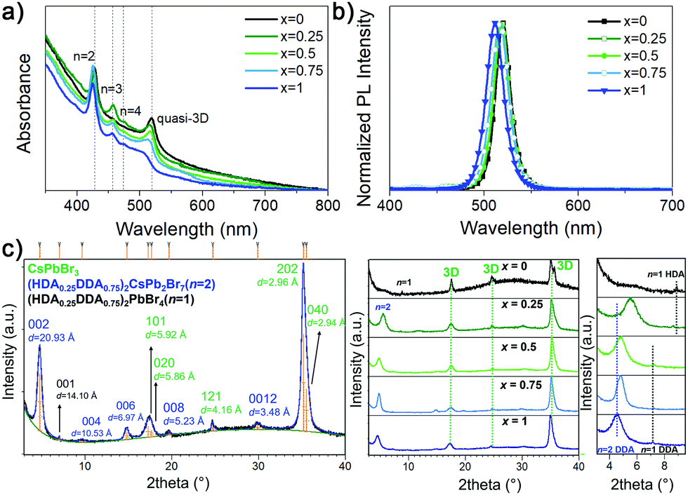 | ||
| Fig. 1 (a) Absorption spectra (with indicated peak positions corresponding to different phases), (b) normalized PL spectra and (c) X-ray diffraction patterns of (DDAxHDA1−x)Csn−1PbnBr3n+1 films with different DDA content x. | ||
We have previously demonstrated that mixing of the spacer cations for quasi-2D RP films results in the change of film composition in terms of distribution of phases with different n.13 Here we can also observe that the film composition (DDA:HDA ratio) significantly affects the distribution of different n phases in the samples (characteristic excitonic features of low n phases and quasi-3D phase are marked in Fig. 1a). In the case of pure HDA, dominant phases in the absorption spectra of the sample are n = 2 and quasi-3D (3D phase and very large n phases cannot be distinguished, hence we label this as quasi-3D), which results in unfavourable energy landscape for efficient funneling and consequently less efficient light emission compared to DDA-containing samples which show the evidence of the presence of n > 2 quasi-2D phases between n = 2 and quasi-3D in the absorption spectra. In addition, HDA sample also exhibits larger number of pinholes, and the pinholes diminish with increasing DDA content. The PL spectra of all samples exhibit emission from quasi-3D phase. The phase compositions of samples with different x additionally were investigated by the XRD analysis. In the diffraction pattern of pure HDA sample, we observe the diffraction lines belonging to n = 1 and 3D phase. The structure of CsPbBr3 crystallizes in orthorhombic Pnma space group with unit-cell parameters a = 8.245(2) Å, b = 11.731(2) Å and c = 8.181(5) Å which is in an accordance with a structure determined by Stoumpous et al.31 With the addition of DDA, additional reflections belonging to n = 2 phase appear. It is particularly interesting to notice the influence that the length of spacer cations has on the c-direction periodicity, for both n = 1 and n = 2 phases, as x increases. Refined position of 001 line (d = 11.57 Å) in pure HDA sample corresponds to the structure of HDA2PbBr4 reported by Mousdis et al.32 while n = 1 phase (d = 14.49 Å) found in pure DDA sample corresponds to the DDA2PbBr4 structure reported by Lemmerer and Billing.33 Typically, when considering a partial substitution of small cations having different sizes on crystallographic A site or partial substitution of different halide anions on crystallographic B site, one expects to notice a continuous shift of diffraction lines as a function of x towards lower or higher angles, depending on the size difference between original and dopant atom/ion. Such continuous trend has not been observed, nor should it be necessarily expected, for the partial exchange of A′ cations, since such an exchange does not include substitution of different atoms/ions on the exact same crystallographic site(s) but instead it comprises of reorganization of spacer layer, often accompanied with conformational changes of one or both A′ cations that happen once the certain ratio of two cations is reached. Considering 001 diffraction line of n = 1 phase, we can observe that mixed HDA–DDA sample with x = 0.25 exhibits a similar periodicity along c-direction as pure HDA sample while the spacer layer thickness in samples with x = 0.5 and 0.75 is almost the same as in pure DDA sample. Obviously, the thickness of the spacer layer in n = 1 phase in sample x = 0.25 is mainly governed by the length of HDA cation since HDA is present in larger amount than DDA. This, at the same time, also means that longer DDA is forced, but also able, to change its conformation and/or orientation and adopt itself to the bilayer thickness as dictated by the shorter HDA cation. With the further increase in x, no significant shift of 001 lines is observed suggesting that spacer layer thickness in mixed HDA–DDA phase with DDA content ≥50% is mainly dominated by longer cation which seems to adopt a very similar packing to that in pure DDA phase. The same is noticed in n = 2 phase; layer thickness of mixed n = 2 phase in sample with x = 0.25 is governed by shorter HDA cations. Once the amount of DDA increases to be equal or larger than x = 0.5, the packing arrangements within the spacer layer become mainly influenced by longer DDA. Similar behaviour was established for BA–PEA RP perovskites where the unit cell dimensions of mixed phase were also governed by the longer PEA cation.13
We investigated the LED performance of the perovskite films with different DDA:HDA ratio x, and the obtained results are summarized in Table S1 (ESI†) and shown in Fig. 2. We can observe that the efficiency and luminance of DDA-containing devices is significantly higher compared to that of HDA only devices, and that (DDAxHDA1−x)Csn−1PbnBr3n+1 devices exhibit improved performance for optimized value of x = 0.75 compared to pure DDA. The EQE variation with composition is consistent with trends observed for photoluminescence quantum yield (PLQY), also shown in Table S1 (ESI†). To examine the reasons for this, transient absorption (TA) measurements and time resolved photoluminescence (TRPL) were measured, as shown in Fig. 3. TA measurements enable examination of the effectiveness of charge transfer between different phases in the samples.4,6,10
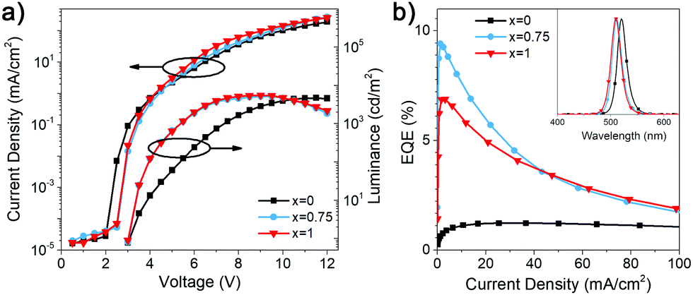 | ||
| Fig. 2 (a) J–V–L curves of (DDAxHDA1−x)Csn−1PbnBr3n+1 based LED devices with x = 0, 0.75, and 1, respectively. (b) EQE versus current density of (DDAxHDA1−x)Csn−1PbnBr3n+1 based LED devices with x = 0, 0.75, and 1, respectively. The inset shows the normalized EL spectra of the corresponding devices. | ||
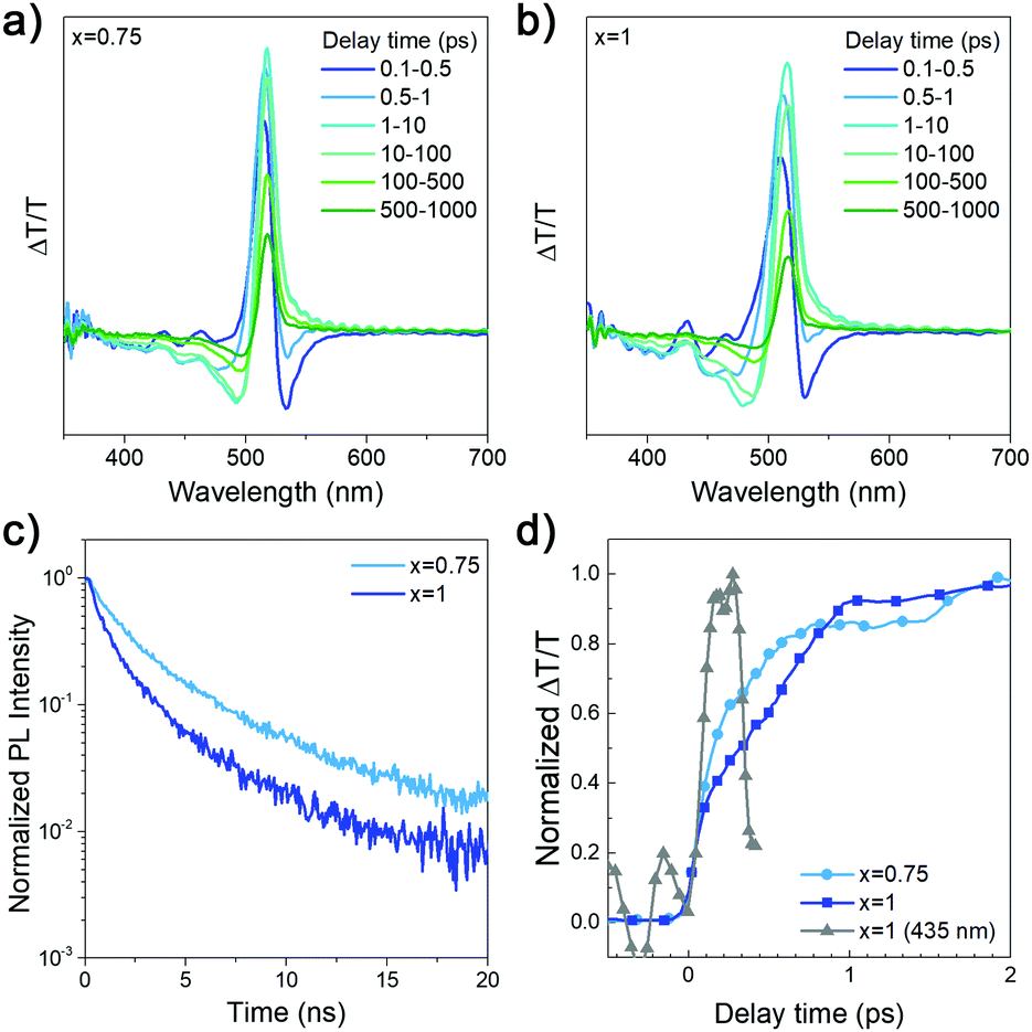 | ||
| Fig. 3 (a and b) Transient absorption spectra and (c) time resolved PL spectra of (DDAxHDA1−x)Csn−1PbnBr3n+1 films with x = 0.75 and 1, respectively; (d) TA kinetics probed at the peak wavelengths ∼518 nm and ∼516 nm for x = 0.75 and x = 1 respectively. The normalized kinetics of x = 1 sample probed at 435 nm (n = 2) peak in grey, shows its fast increase within the pulse resolution in comparison to the slower growth of the GSB probed at the quasi-3D peak of x = 1 sample in dark blue. | ||
From the TA spectra, we observe a large positive signal matching the absorption onset at ∼520 nm, which we attribute to the ground state bleach (GSB) of the quasi-3D phases. To the higher energy side of the TA spectra, we observe a series of relatively weak positive and negative peaks. The positive peaks lie at ∼430 nm and ∼460 nm, which coincides with the high energy sharp peaks in the absorption spectra in Fig. 1a. We hence attribute the TA signal at these positions as the GSB of the lower n-number phases (n = 2, 3). As observed in Fig. 3d, the signal from these high energy peaks arises almost instantaneously whereas the GSB at ∼520 nm grows subsequently in the ps time scale. Overlapping with the high energy peaks is a strong PA signal which has been attributed to changes in refractive index leading to a high energy negative feature.34 Due to the very weak high energy signal, and the large negative signal overlap, it is difficult to reliably extract, the kinetics of the high energy peaks. However, by probing the quasi-3D phase at the peak wavelength, we can observe the funneling dynamics by the rise-time of the GSB signal, as the carrier concentration of the quasi-3D phases gradually increases (Fig. 3d). The x = 0.75 sample rises faster than the x = 1 sample suggesting more efficient funneling from higher bandgap to lower bandgap phases, which is likely due to differences in the sample microstructure. From the slower TRPL decay obtained for x = 0.75, we can conclude that this composition leads to more efficient radiative recombination, consistent with more efficient funneling and obtaining the same luminance for lower current compared to x = 1 samples.
To try to further improve the performance of the devices, we examined the effect of passivation. Using additives for defect passivation and/or emission efficiency enhancement is commonly used for both RP and DJ-based PeLEDs.6,7,16,24 For example, treatment with different molecules, such as trioctylphosphine oxide (TOPO)11 or triphenylphosphine oxide (TPPO)24 is commonly used to enhance the efficiency of PeLEDs. Specifically, TPPO passivates uncoordinated Pb2+, which reduces trap density and increases emission efficiency.24 In addition, TPPO can also enhance the emission efficiency by improving the morphology of the FAPbBr3 films,25 but we have not observed significant effects of TPPO on sample morphology in our samples, as shown in Fig. S1d and e (ESI†).
TPPO also provides edge stabilization in quasi-2D RP perovskite materials.26 From Fig. 4 and Table S1, ESI,† we can observe an increase in the PLQY and EQE, but a drop in maximum luminance and a faster efficiency roll-off with increasing current. Interestingly, low efficiency pure HDA devices did not exhibit efficiency drop with increasing current density. The TPPO passivation also results in less pronounced absorption peaks corresponding to lower n phases, as shown in Fig. S3 (ESI†). The change in the phase distribution of the sample is also evident from a small red shift of the PL peak, while the EL peak position remained unchanged. In some perovskite LEDs, a quick drop-off of emission intensity is observed at large currents despite an increase in maximum EQE and the suppression of traps after using an additive,6 and improvement in the performance was attributed to changes in the charge transfer dynamics among different n phases.6 Based on the obtained results, improved performance with TPPO can likely be attributed to a change in sample phase distribution and consequently a change in the funneling kinetics.
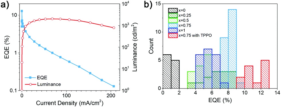 | ||
| Fig. 4 (a) Luminance and EQE as a function of current density for (DDA0.75HDA0.25)Csn−1PbnBr3n+1 based LED device with TPPO passivation; (b) EQE histograms of (DDAxHDA1−x)Csn−1PbnBr3n+1 based LED devices with various DDA content x and passivation conditions. | ||
To examine the defect density in the samples, we performed SCLC19,28 measurements to estimate trap density. Obtained results are summarized in Table S2 and Fig. S4 (ESI†). We can observe a somewhat counterintuitive result that HDA samples exhibit lower trap density. Thus, we can conclude that the low efficiency can be attributed to inferior film morphology and inefficient funneling.
We have also examined the stability of the devices, since DJ perovskites are expected to exhibit good stability. However, while NIR-emitting DJ LEDs exhibit long lifetimes equal or exceeding T50 = 100 h,4,6 blue DJ LEDs exhibited much shorter lifetime, 109 s without Rb and 3.6 min with Rb,5 while T50 value for green DJ LED7 has not been reported. The obtained results for the device stability are shown in Fig. 5, and summarized in Table S1 (ESI†). We can observe that devices with x = 0.75 and x = 1 exhibit significantly longer lifetime compared to other compositions, as well as a different shape of the luminance vs. time curve. For these two compositions, we observe first a small increase in luminance followed by a slow decrease, while for other compositions we observe a steady decrease. An increase of initial luminance followed by a decrease has been reported in different PeLEDs,4,5,26 while in some devices a decrease is observed.4,26 Possible reason for low lifetime of HDA-based devices is the existence of pinholes in the perovskite film, as well as the fact that higher bias is needed due to lower efficiency, which would result in increased Joule heating, causing lower T50.5 A small increase in luminance followed by slow decrease is often found to be beneficial for overall T50,26,28 compared to steady decrease26 or large luminance overshoot.28 The increase is caused by ion/defect migration (these two phenomena are closely related), leading to the accumulation of charges at interfaces and consequently a modification of charge injection and eventually an increase in luminance due to more efficient charge injection.27,28 Different from ion migration within the perovskite layer which can lead to increased luminance/emission efficiency, ion migration across the interfaces of different layers in the device eventually leads to device degradation.27 Thus, the improved T50 of devices with x = 0.75 and x = 1 can be attributed to initial redistribution of ions/defects, which lead to an initial increase in luminance followed by a slower degradation process. It should be noted that these samples exhibit higher defect density but a more favourable energy landscape for funneling compared to x = 0 samples, which underscores the complexity of relationships between sample structure, defects, ion migration, emission efficiency, and device lifetime.
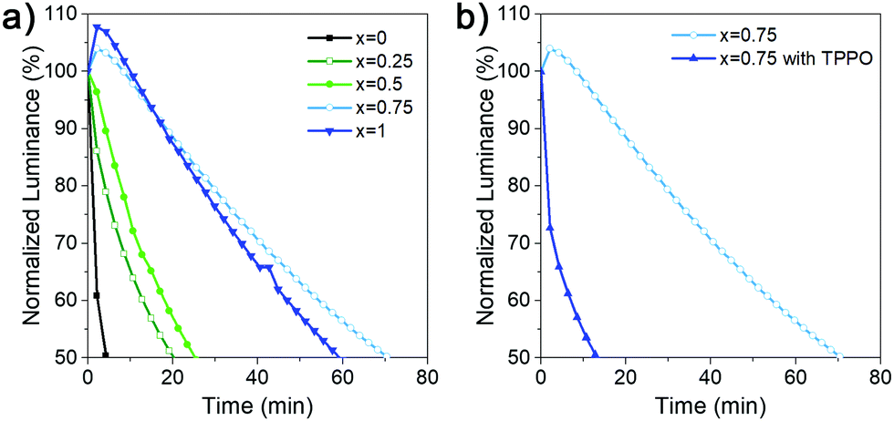 | ||
| Fig. 5 (a) Lifetime of (DDAxHDA1−x)Csn−1PbnBr3n+1 based LED devices with various DDA content x and (b) x = 0.75 with and without TPPO passivation. The lifetime of all devices were characterized with an initial luminance of 100 cd m−2. | ||
In addition to variations in behavior of devices with different x, we can also observe a similar difference in devices with and without TPPO. Different from RP perovskites where TPPO passivation leads to both an increase in EQE as well as T50,26 we observe a decrease in the lifetime despite an increase in the efficiency. Interestingly, in TPPO-passivated PEA2Cs2.4MA0.6Pb4Br13 the passivated LEDs exhibit the pattern of increase followed by decrease of luminance, while steady decrease was observed in control devices, which is opposite from what we observe in our work.26 Consequently, we can conclude that while TPPO can passivate some nonradiative defects in DJ perovskites, the defect nature is likely different compared to RP perovskites due to the use of diammonium spacer cations.
Conclusion
We demonstrated efficient green emission from Dion–Jacobson perovskites with mixed DDA–HDA spacer cations, with a maximum EQE of 9.41% for the optimized ratio of DDA:HDA, which could be further increased to 12.85% after TPPO passivation. The efficiency enhancement could be attributed to more favourable phase distribution in the films, since the absence of n = 2, 3, etc. phases in HDA films is unfavourable for energy funneling, resulting in poor efficiency of HDA-only perovskites, which is further exacerbated by the presence of pinholes in the films. The addition of DDA improves the film morphology and results in the appearance of n = 2 phase, even for low DDA content of 0.25 where the periodicity along the c axis is still dominated by the HDA cation. Thus, we show that, similar to RP perovskites, the phase composition of the film and the emission efficiency and stability can be optimized by spacer cation mixing approach.
Experimental section
Materials
Lead(II) bromide (PbBr2, 98%), cesium bromide (CsBr, 99.999%), and ethanolamine (≥99%) were purchased from TCI. 1,6-Hexanediammonium dibromide (HDABr2), 1,10-decanediammonium dibromide (DDABr2), formamidinium bromide (FABr), and poly[(9,9-dioctylfluorenyl-2,7-diyl)-alt-(4,4′-(N-(4-butylphenyl)))] (TFB) were purchased from Xi’an Polymer Light Technology Corporation. Triphenylphosphine oxide (99%) and chlorobenzene (anhydrous, 99.8%) were purchased from Acros Organics. Nickel(II) acetate tetrahydrate (Ni(Ac)2·4H2O, 99.998%), acetonitrile (anhydrous, 99.8+%), 2-propanol (anhydrous, 99.5+%) and dimethyl sulfoxide (DMSO, anhydrous, 99.9%) were purchased from Alfa Aesar. Hexafluorotetracyano-naphthoquinodimethane (F6TCNNQ, 99%), 1,3,5-tris(1-phenyl-1H-benzimidazol-2-yl)benzene (TPBi, >99.8%), and 8-hydroxyquinolinolato-lithium (Liq, >99.9%) were purchased from Luminescence Technology Corporation. Aluminum pellets (Al, 99.999%) were purchased from Kurt J. Lesker Company. All materials were directly used as received.Synthesis of perovskite thin films
A stock solution was prepared by dissolving CsBr and PbBr2 with the molar ratio of 1:1 in DMSO. The concentration of the stock solution as determined by Pb2+ is 0.4 M. The spacer solution was prepared by dissolving DDABr2 or HDABr2 in DMSO at a concentration of 0.1 M, respectively. Prior to the synthesis of perovskite thin films, the solutions of DDABr2 and HDABr2 were mixed at a volume ratio of x:1 − x, where x = 0, 0.25, 0.5, 0.75, & 1. The spacer solution was further mixed with the stock solution of CsBr–PbBr2 at a volume ratio of 1:1, resulting in a precursor solution at a Pb2+ concentration of 0.2 M.
20 μL of DMSO was added at the circular edge of a Petri dish (φ 60 mm, with lid) at least 10 min before use. The precursor solution was spin coated on the cleaned glass substrate at 5000 rpm for 35 s. Immediately after the spin coating process, the substrate was placed at the center of the Petri dish covered with the lid and kept inside for 90 s to complete the vapor annealing process. The film was further annealed at 80 °C for 2 min to remove the excess DMSO residue.
Optical and morphological characterizations of perovskite thin films
Absorption spectra of the perovskite films were obtained using a Cary 60 UV-Vis Spectrometer (Agilent Technologies). Room temperature PL spectra were measured in ambient with a HeCd (325 nm) laser as the excitation source, and the spectra were collected using a PDA-512USB (Control Development Inc.) Fiberoptic Spectrometer. XRD patterns of the perovskite samples were characterized with Rigaku MiniFlex 600-C X-ray Diffractometer with Co Kα radiation. Top and cross-section view scanning electron microscopy (SEM) was performed using a Hitachi S-4800 FEG Scanning Electron Microscope. PLQY values were measured using Edinburgh instruments FS5 spectrofluorometer and/or determined according to previously reported method.13Time resolved photoluminescence (PL) was measured using a frequency doubled pulsed excitation from a femtosecond Ti:sapphire laser (Coherent Mira 900) operating a 4.2 MHz with an output tuned to 400 nm. The excitation beam was focused onto the sample and PL was collected by an achromatic lens and diverted into a spectrometer (Acton Spectrapro 275) through a 450 nm laser excitation filter. The spectrometer equipped with a 1200 lpmm grating disperses the peak PL wavelength on to a photon counter (Becker and Hickl PMC100) where time correlated single photon counting was performed with a Becker and Hickl SPC photon counting device.
Transient absorption measurement was performed using a home built pump probe setup. A Ti:sapphire seed oscillator pumped (Coherent Mira 900) regenerative amplifier (Coherent Legend Elite), producing a 100 fs pulses at 3.3 mJ of 800 nm fundamental beam at 1 kHz repetition rate. The fundamental beam is split into two paths, one of the paths enters an optical parametric amplifier (Coherent OPerA Solo) where the pump pulse is generated at 320 nm. This pump beam is diverted onto the sample through a chopper wheel (at 500 Hz) The other split fundamental beam is diverted onto a mechanical delay stage to give time delay between the pump and probe beams. It is then focused onto a 2 mm CaF2 plate which generates a broadband supercontinuum (330–1000 nm) acting as the probe beam. The probe beam is passed through a notch filter at 800 nm to cut out the strong fundamental before being focused onto the sample surface with an achromatic lens, spatially overlapping with the pump beam. The transmission of the probe is measured by a spectrometer with a 50 lpmm grating and detected with a CCD line array synchronized with the probe laser repetition rate. The transmission spectrum is recorded continuously (1 kHz) and every other shot will be overlapped with the pump beam (500 Hz). Differential signal is then carried out at each time delay point by (Ton − Toff)/Toff. Approximately 1000 spectral pairs are taken for averaging for every time point.
Fabrication and characterization of perovskite LED devices
Patterned ITO/glass substrates were cleaned by sonication in Decon 90, deionized water, acetone, toluene, acetone, and ethanol in sequence, followed by oxygen plasma treatment before use. NiOx sol–gel solution was prepared as previously reported,10 by dissolving 0.2 mmol Ni(Ac)2·4H2O and 0.2 mmol ethanolamine in 1 mL of 2-propanol. The sol–gel solution was stirred at 70 °C for 2 hours to form a homogeneous green solution. The NiOx solution was then spin-coated on cleaned ITO/glass substrates at 4000 rpm for 30 s, followed by annealing at 275 °C in air for 30 min. F6TCNNQ as a molecular dopant was dissolved in acetonitrile at a concentration of 0.2 mg mL−1. The F6TCNNQ solution was spin-coated on the NiOx films at 4000 rpm for 30 s inside an Ar-filled glovebox, followed by annealing at 80 °C overnight for effective doping. A TFB thin layer was prepared on top of the doped NiOx film by spin coating of TFB solution in chlorobenzene at a concentration of 10 mg mL−1, followed by annealing at 120 °C for 30 min. The TFB thin film was subjected to oxygen plasma for 10 s before proceeding with perovskite deposition. The plasma treatment resulted in complete wetting of the TFB surface with perovskite solution, while before the treatment the observed contact angle was 52.7°. Perovskite thin films were then deposited following the procedures described above. The substrates were transferred to the thermal evaporator for thermal deposition of TPBi (40 nm), Liq (2 nm), and Al electrode (100 nm) in sequence. The device area was defined by the cross-sectional area of the bottom ITO contact and top electrode deposited through a shadow mask as 0.04 cm2. The device performance of the perovskite LEDs was characterized using a measurement setup consisting of a programmable Keithley 2400 SourceMeter and a Photoresearch PR-670 spectroradiometer with SL-1X close-up lens. The device lifetime was measured by monitoring the luminescence change of the device under a constant current bias.Conflicts of interest
There are no conflicts to declare.Acknowledgements
This work was supported by the Seed Funding for Basic Research and Seed Funding for Strategic Interdisciplinary Research Scheme of the University of Hong Kong, RGC GRF projects 17301520, RGC CRF project 7035-20G, NSFC project 6207032617, project PZS-2019-02-2068 financed by the “Research Cooperability” Program of the Croatian Science Foundation funded by the European Union from the European Social Fund under the Operational Programme Efficient Human Resources 2014–2020. The authors also acknowledge financial support from Croatian–Chinese bilateral project entitled “Quasi 2D organic–inorganic perovskites for light emitting applications”.Notes and references
- L. Zhang, C. J. Sun, T. W. He, Y. Z. Jiang, J. L. Wei, Y. M. Huang and M. J. Yuan, Light: Sci. Appl., 2021, 10, 61 CrossRef CAS PubMed.
- Y. Han, S. J. Yue and B. B. Cui, Adv. Sci., 2021, 8, 2004805 CrossRef CAS PubMed.
- X. T. Li, J. M. Hoffman and M. G. Kanatzidis, Chem. Rev., 2021, 121, 2230–2291 CrossRef CAS PubMed.
- Y. Shang, Y. Liao, Q. Wei, Z. Wang, B. Xiang, Y. Ke, W. Liu and Z. Ning, Sci. Adv., 2019, 5, eaaw8072 CrossRef CAS PubMed.
- Y. Liu, L. K. Ono, G. Tong, H. Zhang and Y. Qi, ACS Energy Lett., 2021, 6, 908–914 CrossRef CAS.
- K. H. Ngai, Q. Wei, Z. Chen, X. Guo, M. Qin, F. Xie, C. C. S. Chan, G. Xing, X. Lu, J. Chen, K. S. Wong, J. Xu and M. Long, Adv. Opt. Mater., 2021, 9, 2100243 CrossRef CAS.
- C.-H. Chen, Z. Li, Q. Xue, Y.-A. Su, C.-C. Lee, H.-L. Yip, W.-C. Chen and C.-C. Chueh, Org. Electron., 2019, 75, 105400 CrossRef CAS.
- W. Ke, L. Mao, C. C. Stoumpos, J. Hoffman, I. Spanopoulos, A. D. Mohite and M. G. Kanatzidis, Adv. Energy Mater., 2019, 9, 1803384 CrossRef.
- S. Ahmad, P. Fu, S. Yu, Q. Yang, X. Liu, X. Wang, X. Wang, X. Guo and C. Li, Joule, 2019, 3, 794–806 CrossRef CAS.
- F. Liu, X. Qin, B. Han, C. C. S. Chan, C. Ma, T. L. Leung, W. Chen, Y. He, I. Lončarić, L. Grisanti, J. Ovčar, Ž. Skoko, Y. Shi, F. C. C. Ling, M. R. Huqe, J. A. Zapien, S. Wang, C.-J. Su, U.-S. Jeng, K. S. Wong, A. M. C. Ng, M. Gu, J. Popović and A. B. Djurišić, Adv. Opt. Mater., 2021, 2100393 CrossRef CAS.
- X. Yang, X. Zhang, J. Deng, Z. Chu, Q. Jiang, J. Meng, P. Wang, L. Zhang, Z. Yin and J. You, Nat. Commun., 2018, 9, 570 CrossRef PubMed.
- P. Vashishtha, M. Ng, S. B. Shivarudraiah and J. E. Halpert, Chem. Mater., 2019, 31, 83–89 CrossRef CAS.
- T. L. Leung, H. W. Tam, F. Liu, J. Lin, A. M. C. Ng, W. K. Chan, W. Chen, Z. He, I. Lončarić, L. Grisanti, C. Ma, K. S. Wong, Y. S. Lau, F. Zhu, Ž. Skoko, J. Popović and A. B. Djurišić, Adv. Opt. Mater., 2020, 8, 1901679 CrossRef CAS.
- L. Mao, W. Ke, L. Pedesseau, Y. Wu, C. Katan, J. Even, M. R. Wasielewski, C. C. Stoumpos and M. G. Kanatzidis, J. Am. Chem. Soc., 2018, 140, 3775–3783 CrossRef CAS PubMed.
- L. Mao, P. Guo, M. Kepenekian, I. Spanopoulos, Y. He, C. Katan, J. Even, R. D. Schaller, R. Seshadri, C. C. Stoumpos and M. G. Kanatzidis, J. Am. Chem. Soc., 2020, 142, 8342–8351 CrossRef CAS PubMed.
- M. Karlsson, Z. Yi, S. Reichert, X. Luo, W. Lin, Z. Zhang, C. Bao, R. Zhang, S. Bai, G. Zheng, P. Teng, L. Duan, Y. Lu, K. Zheng, T. Pullerits, C. Deibel, W. Xu, R. Friend and F. Gao, Nat. Commun., 2021, 12, 361 CrossRef CAS PubMed.
- D. Liang, Y. Peng, Y. Fu, M. J. Shearer, J. Zhang, J. Zhai, Y. Zhang, R. J. Hamers, T. L. Andrew and S. Jin, ACS Nano, 2016, 10, 6897–6904 CrossRef CAS PubMed.
- J. Byun, H. Cho, C. Wolf, M. Jang, A. Sadhanala, R. H. Friend, H. Yang and T.-W. Lee, Adv. Mater., 2016, 28, 7515–7520 CrossRef CAS PubMed.
- Z. Fang, W. Chen, Y. Shi, J. Zhao, S. Chu, J. Zhang and Z. Xiao, Adv. Funct. Mater., 2020, 30, 1909754 CrossRef CAS.
- Y. P. Fu, X. Y. Jiang, X. T. Li, B. Traore, I. Spanopoulos, C. Katan, J. Even, M. G. Kanatzidis and E. Harel, J. Am. Chem. Soc., 2020, 142, 4008 CrossRef CAS PubMed.
- Y. H. Hu, L. M. Spies, D. Alonso-Álvarez, P. Mocherla, H. Jones, J. Hanisch, T. Bein, P. R. F. Barnes and P. Docampo, J. Mater. Chem. A, 2018, 6, 22215 RSC.
- J. Meng, D. D. Song, D. Huang, Y. Li, Y. Y. Li, A. Maqsood, S. L. Zhao, B. Qiao, H. Zhud and Z. Xu, Phys. Chem. Chem. Phys., 2020, 22, 54 RSC.
- G. Z. Liu, X. X. Xu, S. D. Xu, L. Y. Zhang, H. F. Xu, L. Z. Zhu, X. X. Zhang, H. Y. Zheng and X. Pan, J. Mater. Chem. A, 2020, 8, 5900 RSC.
- Yukta, M. K. Chini, R. Ranjan and S. Satapathi, ACS Appl. Electron. Mater., 2021, 3, 1572 CrossRef CAS.
- D. Y. Jiang, T. Jiang, Y. Tian, K. C. Wen, C. B. Duan, N. N. Wang, Q. Li, J. P. Wang and H. Xu, J. Mater. Chem. C, 2021, 9, 6399 RSC.
- L. N. Quan, D. X. Ma, Y. B. Zhao, O. Voznyy, H. F. Yuan, E. Bladt, J. Pan, F. P. García de Arquer, R. Sabatini, Z. Piontkowski, A. H. Emwas, P. Todorović, R. Quintero-Bermudez, G. Walters, J. Z. Fan, M. X. Liu, H. R. Tan, M. I. Saidaminov, L. Gao, Y. Y. Li, D. H. Anjum, N. N. Wei, J. Tang, D. W. McCamant, M. B. J. Roeffaers, S. Bals, J. Hofkens, O. M. Bakr, Z. H. Lu and E. H. Sargent, Nat. Commun., 2020, 11, 170 CrossRef PubMed.
- Q. Dong, L. Lei, J. Mendes and F. So, J. Phys.: Mater., 2020, 3, 012002 CAS.
- H. B. Kim, J. S. Kim, J. M. Heo, M. Y. Pei, I. H. Park, Z. Liu, H. J. Yun, M. H. Park, S. H. Jeong, Y. H. Kim, J. W. Park, E. Oveisi, S. Nagane, A. Sadhanala, L. J. Zhang, J. J. Kweon, S. K. Lee, H. C. Yang, H. M. Jang, R. H. Friend, K. P. Loh, M. K. Nazeeruddin, N. G. Park and T. W. Lee, Nat. Commun., 2020, 11, 3378 CrossRef PubMed.
- Y. Q. Shang, G. Li, W. M. Liu and Z. J. Ning, Adv. Funct. Mater., 2018, 28, 1801193 CrossRef.
- Y. Liang, Q. Y. Shang, M. L. Li, S. Zhang, X. F. Liu and Q. Zhang, Adv. Funct. Mater., 2021, 31, 2106108 CrossRef CAS.
- C. C. Stoumpos, C. D. Malliakas, J. A. Peters, Z. Liu, M. Sebastian, J. Im, T. C. Chasapis, A. C. Wibowo, D. Y. Chung, A. J. Freeman, B. W. Wessels and M. G. Kanatzidis, Cryst. Growth Des., 2013, 13, 2722 CrossRef CAS.
- G. A. Mousdis, G. C. Papavassiliou, C. P. Raptopoulou and A. Terzis, J. Mater. Chem., 2000, 10, 515 RSC.
- A. Lemmerer and D. G. Billing, CrystEngComm, 2012, 14, 1954 RSC.
- M. B. Price, J. Butkus, T. C. Jellicoe, A. Sadhanala, A. Briane, J. E. Halpert, K. Broch, J. M. Hodgkiss, R. H. Friend and F. Deschler, Nat. Commun., 2015, 6, 8420 CrossRef CAS PubMed.
Footnote |
| † Electronic supplementary information (ESI) available. See DOI: 10.1039/d1tc04743d |
| This journal is © The Royal Society of Chemistry 2022 |