
Electromagnetic interference shielding materials: recent progress, structure design, and future perspective
Xiao-Yun
Wang†
ab,
Si-Yuan
Liao†
ab,
Yan-Jun
Wan
 *a,
Peng-Li
Zhu
*a,
You-Gen
Hu
a,
Tao
Zhao
a,
Rong
Sun
a and
Ching-Ping
Wong
c
*a,
Peng-Li
Zhu
*a,
You-Gen
Hu
a,
Tao
Zhao
a,
Rong
Sun
a and
Ching-Ping
Wong
c
aShenzhen Institute of Advanced Electronic Materials, Shenzhen Institute of Advanced Technology, Chinese Academy of Sciences, Shenzhen 518055, China. E-mail: yj.wan@siat.ac.cn; pl.zhu@siat.ac.cn
bUniversity of Chinese Academy of Sciences, Beijing, 100049, China
cSchool of Materials Science and Engineering, Georgia Institute of Technology, Atlanta 30332, USA
First published on 14th December 2021
Abstract
The rapid development of electronic equipment and the sharp increase in the demand for wireless communication have resulted in a substantial increase in electromagnetic pollution. Consequently, electromagnetic interference (EMI) shielding materials have been developed to solve the grim problem of electromagnetic pollution. However, 5G communication technology and modern electronic products demand shielding materials with higher requirements in terms of EMI shielding performance, weight, flexibility, and reliability. This review focuses on the recent research progress in the structural design, characterization, and properties of various EMI shielding materials including metal type, carbon type, and MXene type. The basic theory of EMI shielding is introduced in detail and the current testing technologies for EMI shielding effectiveness are summarized, which can help elucidate the structural design principles for shielding materials. The effect of different types of carbon materials, which are classified as zero-dimensional, one-dimensional, two-dimensional, and three-dimensional, on the shielding performance, and the corresponding shielding mechanism are discussed. Moreover, near-field shielding and its application in the field of electronic packaging are introduced. Based on our comprehensive analysis, we present the main challenges and outlook of EMI shielding materials in future research.
 Xiao-Yun Wang | Xiao-Yun Wang received her BS degree from Henan Normal University in 2015. Currently, she is working towards her PhD degree at University of Chinese Academy of Sciences under the supervision of Prof. Rong Sun. Her research focuses on the structural design and fabrication of MXene-based EMI shielding materials. |
 Si-Yuan Liao | Si-Yuan Liao received his MS degree from University of Chinese Academy of Sciences in 2021. Currently, he is working towards his PhD degree at University of Chinese Academy of Sciences under the supervision of Prof. Rong Sun. His research mainly focuses on the structural design and synthesis of metal/polymer EMI shielding composites. |
 Yan-Jun Wan | Yan-Jun Wan is an Associate Professor at Shenzhen Institute of Advanced Electronic Materials, Shenzhen Institute of Advanced Technology, Chinese Academy of Sciences. He received his PhD degree at The Chinese University of Hong Kong in 2018. His research interests are focused on EMI shielding materials and functional polymer composites. |
 Peng-Li Zhu | Prof. Peng-Li Zhu obtained her PhD Degree from the Institute of Chemistry, Chinese Academy of Sciences in 2010. Currently, she is working as a Professor in Shenzhen Institutes of Advanced Technology, Chinese Academy of Sciences. Her research interests include metal and metal oxide nanomaterials, EMI shielding materials and functional composite materials used in IC electronic packaging. |
 You-Gen Hu | You-Gen Hu received his PhD Degree from University of Chinese Academy of Sciences in 2017. In 2010, he joined the Shenzhen Institute of Advanced Technology, Chinese Academy of Sciences and became an Associate Professor. Dr Hu works on functional polymer composites such as electronic packaging materials, EMI shielding materials and flexible electronic materials. He is a Youth Editorial Board Member of Soft Science. |
 Rong Sun | Prof. Rong Sun received her PhD Degree from the Lanzhou Institute of Chemical Physics, Chinese Academy of Sciences in 2006. She is currently the Director of the Institute of Advanced Materials Science and Engineering, Shenzhen Institute of Advanced Technology, Chinese Academy of Sciences. Her research interests include flip-chip underfill, through silicon via, thermal interface materials, embedded capacitor inductor resistance, and EMI shielding materials. |
1. Introduction
The popularization of smart electronic devices and wireless communication in the age of artificial intelligence is a source of electromagnetic (EM) wave pollution.1 EM waves are associated with the fields of mobile communication, satellite signals, navigation, and medical equipment.2 Electronics make it convenient to perform daily tasks, however, they generate unwanted EM radiation, resulting in electromagnetic interference (EMI), which affects the performance of electronic products and causes serious harm to human beings. Therefore, whether it is to maintain the normal operation of electronic equipment or to protect human health, EM protection has become an important research field. There are many ways to alleviate the undesirable EM radiation. Usually, a shielding material is placed between the radiation source and the device, which can prevent incoming radiation by absorbing or reflecting EM waves.3 Various materials have been extensively studied and applied in EMI shielding in recent years. The earliest known materials for EMI shielding are metals such as copper, aluminium, and nickel, which provide high electrical conductivity and good mechanical properties, and can be used as a reflective shield.4 In addition, metals and their oxides are very common nano-fillers in nano-composites, and some metal oxides such as Fe3O4 can be used as magnetic fillers to improve the EMI shielding effectiveness (SE) by increasing the absorption of EM waves.5 In addition, ceramics, ferrites, metal magnets, and their composites are also used to attenuate harmful EM waves.6 However, their use as EMI shielding materials used in portable electronic devices and modern electronic equipment is restricted by their high density and low flexibility. Accordingly, higher requirements such as light-weight and flexibility are in demand for EMI shielding materials.As is well known, metals with high electrical conductivity and magnetic permeability possess a high SE. Nevertheless, their heavy weight, easy corrosion, and low flexibility limit their further applications. Hence, numerous relevant studies to overcome these shortcomings of metals in the field of EMI shielding have been carried out in recent years, involving metal/fabric composites, metal transparent films, and metal-type aerogels. Considering this, carbon-type materials such as carbon black (CB), carbon nanotubes (CNT), and graphene provide new candidates for the manufacture of high-performance, light-weight, and flexible EMI shielding materials. CB, which is an easily available carbon product, has been extensively studied in polymer composites for EMI shielding. Besides, one-dimensional carbon-type materials such as CNTs and carbon nanofibers have been widely utilized for high-performance EMI shielding due to their exceptional electrical conductivity, high aspect ratio, and tunable diameter.7–9 Graphene, a purely two-dimensional (2D) sheet of sp2 hybridized carbon atoms, has become the leading candidate for the fabrication of polymer nano-composites. Graphene aerogel/foam with a porous structure shows high electrical conductivity and low density, which has been proven to be an excellent EMI shielding material and used as a filler for polymer composites with excellent electrical conductivity and EMI shielding performances.10–12 Furthermore, MXenes, a new type of 2D material possessing superior inherent electrical conductivity and excellent mechanical properties, has been developed rapidly and is considered a potential novel EMI shielding material.13 Thus, an effective strategy to achieve enhanced EMI shielding performances and meet the practical requirements is to construct hybrid systems with conductive carbon-type materials and magnetic particles.
Herein, we review recent advances on various EMI shielding materials including metal-type, carbon-type and MXene-type (Fig. 1). The effect of different carbon-type materials, which are classified as zero-dimensional, one-dimensional, two-dimensional, and three-dimensional on the shielding performance is summarized, and the corresponding shielding mechanism is discussed. The effect of the structure and morphology of a material on its EMI shielding performance is analyzed. In the first part, we introduced the basic theory of EMI shielding in detail. The electrical conductivity, permittivity, permeability, frequency, and thickness of shielding materials have a great influence on their reflection and absorption of EM waves. Afterward, the fabrication process, structure, and EMI shielding performance of different types of shielding materials including metals, carbon and MXenes are discussed. Moreover, we introduce the application scenarios and test methods of near-field shielding. Finally, prospective research opportunities and outlook on shielding materials are prospected. We believe that this short review can help in understanding the current research status and may find possible research directions to solve existing bottlenecks in the field of EMI shielding materials.
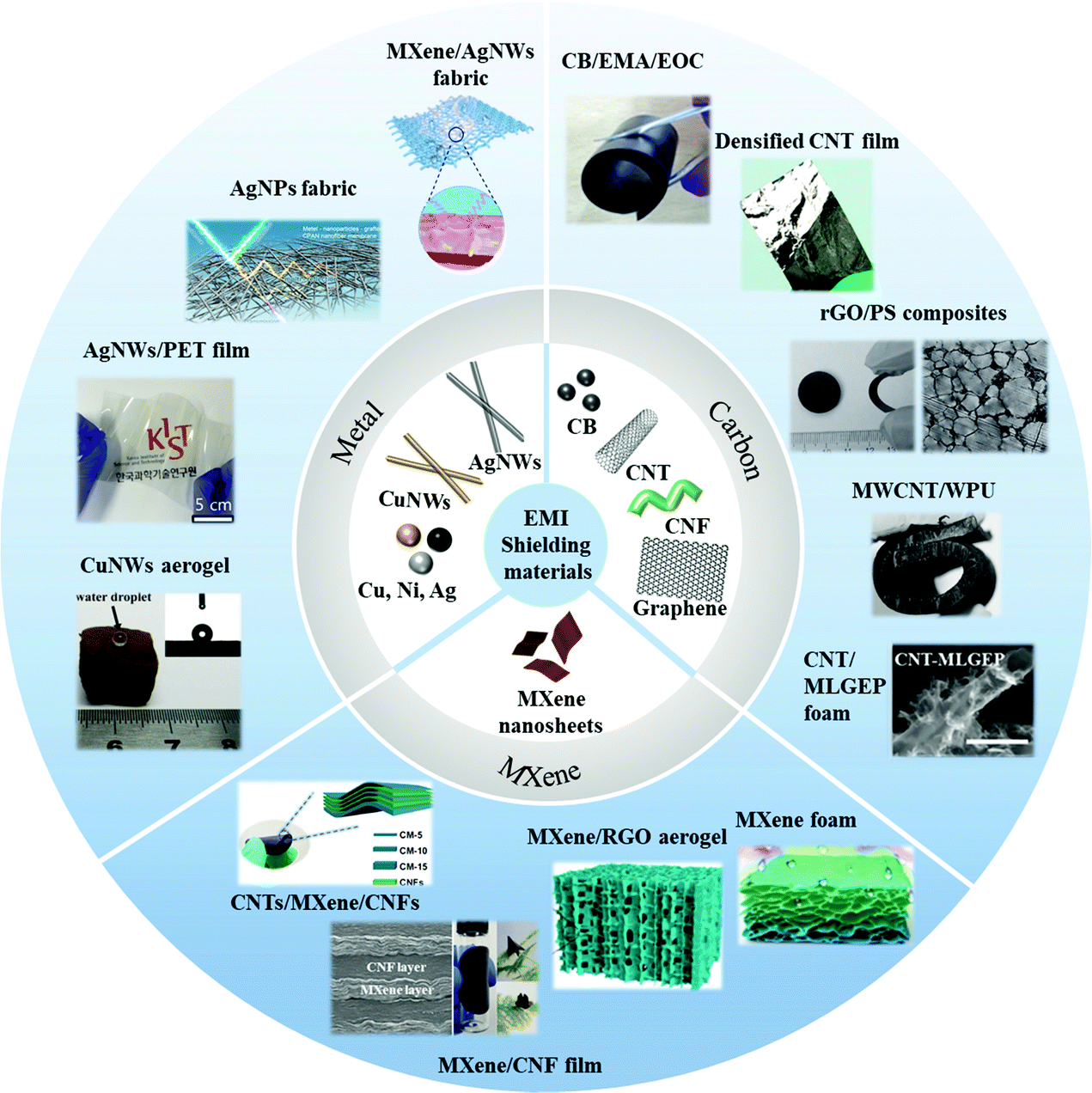 | ||
| Fig. 1 Schematic illustration of electromagnetic interference shielding materials. Copyright 2014 Wiley-VCH Verlag GmbH and Co. KGaA, Weinheim. Copyright 2018, the American Chemical Society. Copyright 2019, John Wiley and Sons, Inc. Copyright 2018, John Wiley and Sons, Inc. Copyright 2018, Springer Nature. Copyright 2018, John Wiley and Sons, Inc. Copyright 2020, the American Chemical Society. Copyright 2017, John Wiley and Sons, Inc. Copyright 2015, John Wiley and Sons, Inc. Copyright 2017, John Wiley and Sons, Inc. Copyright Springer Nature. Copyright 2018, the American Chemical Society. Copyright 2020, the American Chemical Society. | ||
2. Basic theory of EMI shielding
2.1. Shielding mechanism
The shielding of EM waves is the use of shielding bodies to limit the propagation of EM waves in space. The types of EMI shielding can be divided into electric field shielding, magnetic field shielding, and EM field shielding. For electrostatic field shielding, a Faraday cage cavity can be used to protect EM-sensitive equipment. In an external electric field with an electric field strength of E, the free electrons in the conductor will move against the direction of the electric field, thus inducing both sides of the conductor to generate charges with the same electric field strength and opposite electric potential (Fig. 2A).14 In the state of electrostatic equilibrium, the electric field intensity inside the conductive cavity is zero. Thereby, the shell of the conductor cavity protects the electronic equipment placed inside from the influence of the external electric field. Magnetic field shielding is generally aimed at low-frequency EM waves (Fig. 2B).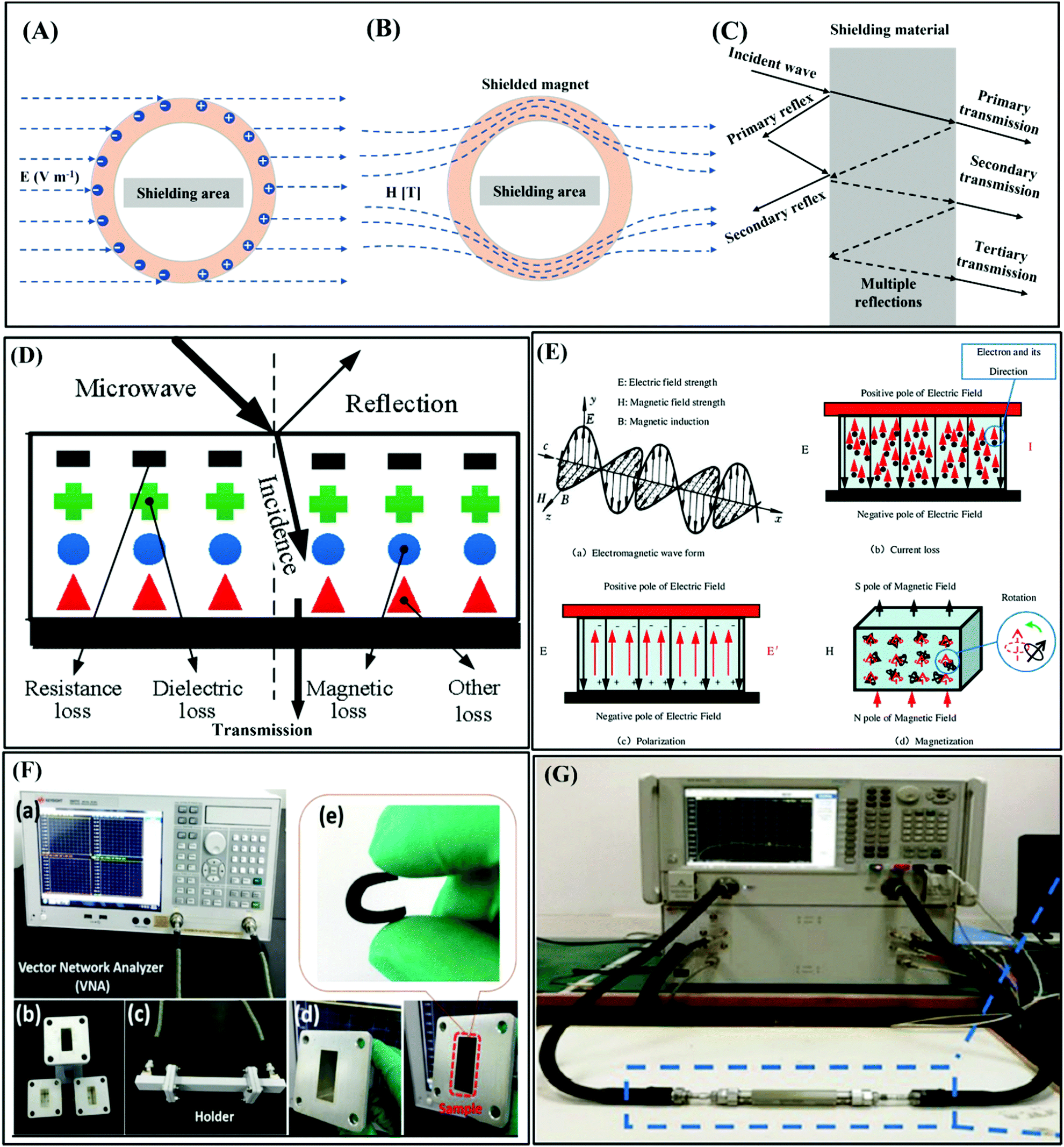 | ||
| Fig. 2 Schematic diagram of EMI shielding mechanism of (A) external electric field and (B) low-frequency magnetic field.14 Copyright 2021, Springer Nature Switzerland AG. Part of Springer Nature. (C) Schematic diagram of EMI shielding mechanism based on transmission line theory. (D) and (E) Schematic representation of EMI shielding mechanisms.2,15 Copyright 2020, Elsevier Ltd. (F) Rectangular waveguide experimental setup and fixture for EMI SE measurement.16 Copyright 2018, John Wiley and Sons, Inc. (G) EMI shielding measurement setup of coaxial line method.17 Copyright 2018, John Wiley and Sons, Inc. | ||
On the one hand, the skin effect of low-frequency EM waves is very small, resulting in small absorption loss. On the other hand, the wave impedance of low-frequency EM waves is minimal, leading to slight reflection loss. Therefore, in the case of magnetic field shielding, it is challenging to rely on absorption loss and reflection loss to achieve effective shielding in the low frequency. For low-frequency magnetic fields, high permeability materials are usually used to provide magnetic bypass to achieve shielding, where a magnetic field is concentrated in the shielding material with low magnetic resistance, shielding the sensitive components placed in the middle from magnetic interference. For an alternating EM field with changes in both electric and magnetic fields, the electric and magnetic properties should be considered. Fig. 2C displays a schematic diagram of the EMI shielding mechanism based on transmission line theory. The shielding mechanism includes three parts, i.e., reflection, absorption, and multiple reflection. Typically, when incident EM waves impact the surface of shielding materials, most of the EM waves are firstly reflected due to the impedance mismatch between the external free space and the shielding materials.18 Residual EM waves penetrating the surface of shielding materials are attenuated inside the material. Meanwhile, this part of the EM waves is reflected many times between the different layers inside the shielding material until it is fully absorbed and eventually dissipated as heat.19–21 Generally, the types of attenuation of EM waves are mainly divided into resistance loss, dielectric loss, magnetic loss, and other losses (such as the destructive interference caused by the incident and reflected EM waves), as shown in Fig. 2D.2 To achieve high-performance EMI shielding, materials should possess either mobile charge carriers or electric and magnetic dipoles, which can interact with incident waves to reflect and absorb EM waves. Furthermore, dipole polarization occurs when the alternating EM field encounters polar groups inside the shielding material to delay the EM waves and synergistically improve the overall shielding performance of the materials (Fig. 2E). For magnetic shielding materials, magnetic loss, including magnetic hysteresis loss, eddy current losses, and relaxation loss, will be also induced by an alternating current magnetic field, which cooperates with current loss, polarization loss, etc. to create higher losses to attenuate incident EM waves.22
2.2. Shielding effectiveness (SE)
EMI SE is an indicator to evaluate the decay ability of materials against EM waves.23 Theoretically, the EMI SE of conductive materials can be expressed by the Simon formalism.24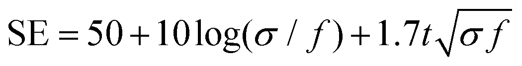 | (1) |
SEp = 10![[thin space (1/6-em)]](https://www.rsc.org/images/entities/char_2009.gif) log(Pin/Pout) log(Pin/Pout) | (2) |
| SEE = 20log(Ein/Eout) | (3) |
| SEH = 20log(Hin/Hout) | (4) |
For EMI shielding materials, the energy loss relation of the incident EM waves after passing through the shielding material can be expressed as eqn (5) and (6):
| A + R + T = 1 | (5) |
| SET = SEA + SER + SEM | (6) |
In addition, SEA is also related to the skin depth (δ) and shielding thickness (d) and is defined as formula (7).26
| SEA = 20(d/δ)loge = 8.686(d/δ) | (7) |
log[T/(1 − R)], the value of SEA greatly increases due to the smaller denominator. Consequently, for almost all reported conductive shielding materials, the value of SEA is higher than the value of SER. Indeed, these are two different evaluation systems. SEA, SER and SET are used to evaluate the shielding mechanism of materials from an EM energy point of view, while R, A, and T are used to evaluate the shielding mechanism from an EM power point of view. Thus, determining the shielding mechanism roughly by simply comparing SEA and SER is one-sided, and they are insufficient to clarify the complex attenuation process of EM waves. Therefore, it is necessary to carefully distinguish the difference between SE (SEA and SER) and power coefficient (A and R) when discussing the shielding mechanism.
2.3. Skin depth effect
The electric field attenuation of EM waves mainly occurs on the surface of the shielding material, and EM radiation at high frequency only penetrates the near-surface region of an electrical conductor, which is known as the skin effect (δ) and expressed as: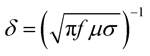 | (8) |
622 S m−1, and it is calculated that δ = 17.33 μm at the frequency of 8.2 GHz.18
2.4. Specific SE (SSE)
For light-weight and porous foam shielding materials, we also need to consider the important factor of mass density. A specific SE (the ratio of EMI SE to density) is usually used to evaluate the overall performance of shielding materials.28 Mathematically, the formula for the calculation of SSE is expressed as eqn (9) and (10), as follows:24,29| SSE(foam) = EMISE/ρ = dB cm3 g−1 | (9) |
For example, Wu et al. prepared Cu NW core–shell aerogels, which exhibited an outstanding EMI SE of up to 52.49 dB and ultra-light density of up to ∼1.65 × 10⁻³ g cm−3, and substituting these the data into eqn (9), the specific SE can be calculated as ∼31812 dB cm3 g−1.30 In addition, the SSE of the Ag@C aerogel developed by our group reached 67015 dB cm3 g−1 according to the above-mentioned equation.16 In particular, the SSE value (foam) is closely related to the thickness of the shield. Hence, a reference parameter of EMI shielding materials with a porous structure should be introduced. This formula is expressed as the EMI SE value divided by the areal density, which means SE per surface density.31
| SSE/t(foam) = EMISE/(ρ × t) = dB cm2 g−1 | (10) |
The SSE (foam) parameter incorporating three elements of EMI SE, density, and thickness is used to comprehensively evaluate the EMI shielding capability of materials.32 For instance, Qiang Song et al. reported the preparation of a CNT–graphene hybrid foam, showing an EMI SE of 38 dB at a density of ≈0.0058 g cm−3, where the SSE/t value of the foam with a thickness of 1.6 mm its about 40000 dB cm2 g−1 by calculation.33 However, for a shielding film, its thickness plays an important role in determining the SE. Therefore, the SSE is defined as EMI SE divided by thickness. The SSE value can be calculated using eqn (11), as follows:
| SSE(film) = EMISE/thickness = dB mm−1 | (11) |
For example, Zeng et al. designed a Cu-wrapped polymer nanofiber membrane with an EMI SE of 44.7 dB and thickness of 1.2 μm, where the SSE of this film by calculation using eqn (11) is ∼37250 dB mm−1.34 The SSE of the iodine-doped large graphene paper prepared our group reached 4176 dB mm−1. Therefore, for different types of shielding materials, such as films, foams, and aerogels, it is necessary to employ appropriate SSE definitions to compare their shielding performances.
2.5. Measuring method of EMI shielding effectiveness
The EMI SE value of shielding materials is calculated based on the S parameters, which are measured using a vector network analyzer (VNA). There are different methods to measure the EMI SE, including co-axial transmission line method, open field method, shielded box method and shielded room method. The coaxial transmission line method is commonly adopted to record the S parameters in a broad range of frequencies (as shown in Fig. 2F), in which both the waveguide and air-line can be served as fixtures. By employing the waveguide method, the total EMI SE, SE absorption and SE reflection can be achieved. Furthermore, the corresponding power coefficients of reflectivity (R), absorptivity (A), and transmissivity (T) calculated from the S parameters can help understand the EMI shielding mechanism.35 When measuring the EMI SE of shielding materials using the rectangular waveguide method, the sample needs to be cut into a rectangular shape with different sizes to meet the fixture for different frequency bands. Typically, EM waves have an incident power of 0 dBm, corresponding to 1 mW in this method. The test frequency band of the rectangular waveguide method is from 0.96 GHz to 112 GHz. Accordingly, the size of the rectangular waveguide fixture is gradually reduced. Particularly, 8.2–12.5 GHz, i.e., the so-called X-band, is the most extensively studied in the literature because it is widely used in communication applications such as telephones, microwaves, and TV picture transmission.36,37 Typically, specimens with different thicknesses are cut into 22.86 × 10.16 mm (length × width) to well fit the waveguide fixture. The EMI SE of shielding materials can calculated using the scattering parameters (S11 and S21), which are obtained from VNA equipment using eqn (12)–(16), as follows:| R = |S11|2 = |S22|2 | (12) |
| T = |S21|2 = |S12|2 | (13) |
| SET = −10lg|S21|2 = −10lg|S12|2 = −10lg(T) | (14) |
 | (15) |
| SER = −10lg(1 − R) | (16) |
3. EMI shielding materials
3.1. Metal-type EMI shielding material
Due to their characteristics of excellent electrical conductivity and permeability, metallic materials (such as silver, copper, iron, and nickel) are recognized as the important EMI shielding materials for the EMI shielding of electronic devices. Unfortunately, the application of metallic materials in the EMI shielding field is limited by their disadvantages, including high density, non-corrosion resistance, and inability to bend.Hence, numerous relevant studies about overcoming these inherent defects ranging from metal/polymer composites,38 metal/fabric composites, metal-type transparent films to metal type aerogels have been reported. In this chapter, we mainly review the research on metal-type shielding materials with flexibility, light-weight, and corrosion-resistance in recent years, and summarize their EMI shielding performances.
000 S m−1 and SE of above 65 dB with a thickness of about 300 μm in the frequency range of 4–18 GHz.
 | ||
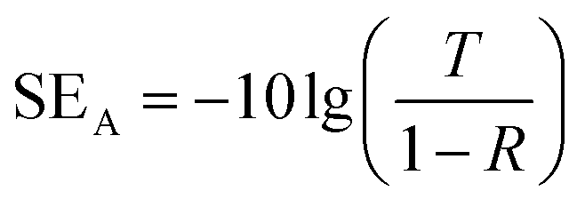
| Fig. 3 (A) Schematic diagram of the manufacture of CPAN NF/MNP hybrid nanofiber membrane.42 Copyright 2018, Springer Nature. (B) Schematic diagram of the preparation process of hydrophobic, permeable, and conductive silk textile.43 Copyright 2019, John Wiley and Sons, Inc. (C) Schematic for the fabrication of the PU–AgNW/CFF fabric.45 Copyright 2018, Elsevier Ltd. | ||
Most conductive fabrics were acquired via the dip coating, spray coating, and printing methods in the past. Nevertheless, these fabrication technologies deteriorate the inherent flexibility and mechanical properties of the textile substrate. In the hope of endowing fabrics with hydrophobicity, while ensuring flexibility and mechanical properties of the substrate, Liu et al. prepared a metal fabric through a vacuum-assisted layer-by-layer assembly technique, in which the interface interaction between the metal particles and polymer was promoted by plasma treatment and deposition of PEI molecules on the fabric.43 The treated textiles were then alternately coated with MXene nanosheets and Ag nanowires to obtain a metal/fabric composite, as shown in Fig. 3B. Interestingly, it was found that the EMI shielding performance of the co-modified fabric was better than that of the single modified fabric owing to the synergistic effect of MXene and Ag nanowires. The MXene sheet could prevent the oxidation of silver and enhance the binding force of silver on the fabric base.
The binding force between the metal and fabric plays a dominated role in the mechanical properties, EMI shielding performance and reliability of metal/fabric composites. In addition, Luo et al. used a polydopamine (PDA)-modified polypropylene (PP) polymer substrate to enhance the adhesion of Ag particles and polymer fibers without active functional groups.44 The fabricated conductive polymer fabric composites possessed outstanding conductivity of 8120 S m−1 and extraordinary EMI SE of around 71.2 dB. The composite material of PP/PDA/Ag NPS metal fiber coated with PDMS exhibits numerous application prospects in aerospace, mobile phone components, and other fields stemming from its characteristics of light weight, favorable electrical conductivity, excellent mechanical stability, and corrosion resistance.
However, the polymer fabric substrate mentioned above is an insulator, which results in poor electrical conductivity, and thus recently researchers have focused their attention on carbon fibers with excellent electrical conductivity as fiber substrates for fabricating the metal/fabric composites with excellent EMI shielding performances. For example, Lee et al. used the electroless plating method to fabricate a metal/fiber composite, where the activated carbon fiber fabric (CFF) was covered with copper particles.46 In addition, Jia et al. also fabricated stretchable and durable conductive metal/carbon fabric materials by integrating silver nanowires and polyurethane on a carbon fiber fabric,45 as shown in Fig. 3C.
The authors found that the EMI SE of the PU–Ag NW/CFF film reached 106 dB in the frequency range of 8.2–12.5 GHz after dip-coating for over 7 times. Further, the mechanical and chemical stability of the PU–Ag NW/CFF film was tested, and the results revealed that the EMI SE was only reduced by 3% after 5000 bends, and the EMI SE was only reduced by 5% and 3% after soaking in strong acid of pH = 2.0 and alkaline solution of pH = 12.0 for 10 h, respectively.
 | ||
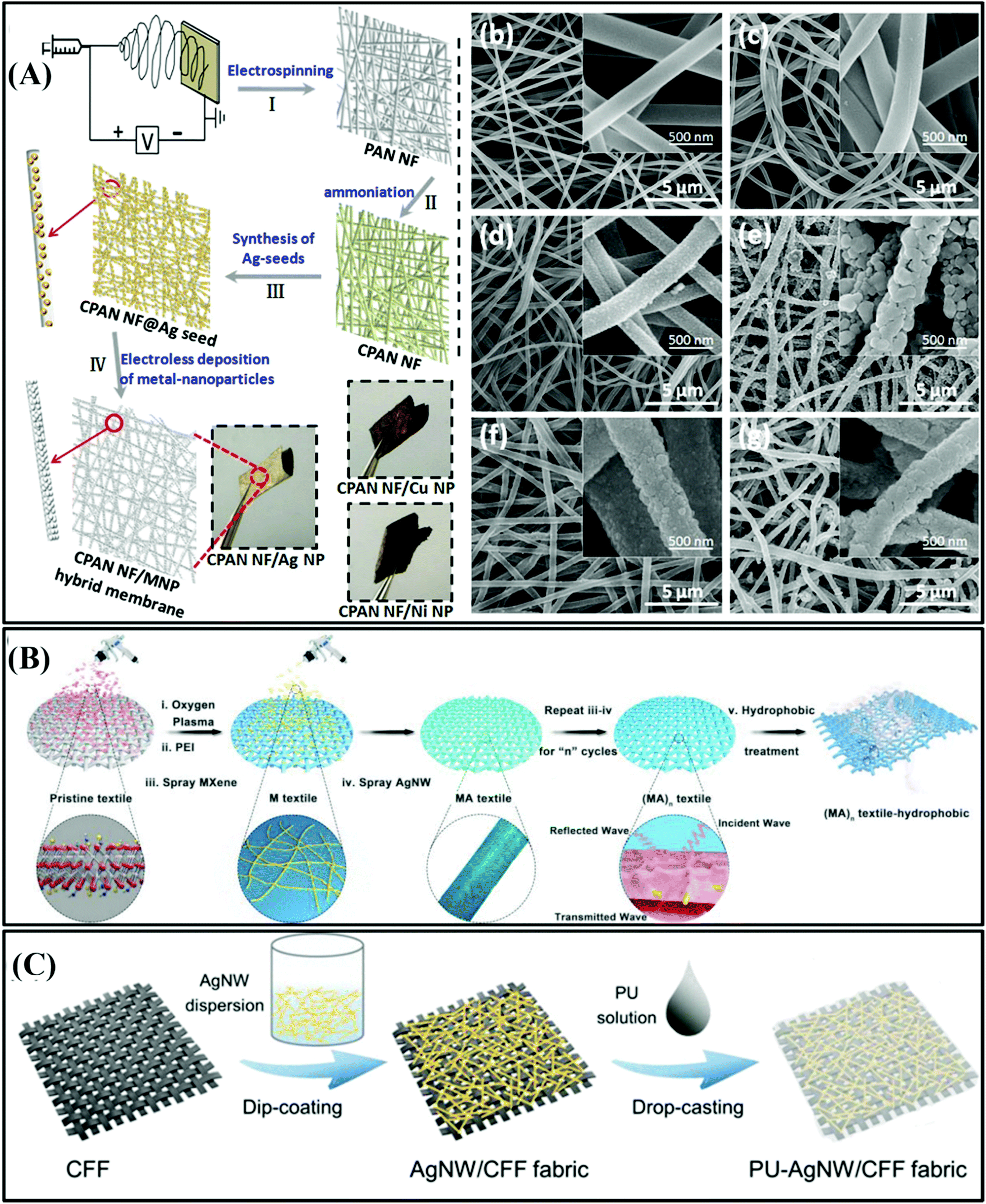
| Fig. 4 (A) Flow chart of the fabrication of the CA/Ag NW/PU film.49 Copyright 2018, the American Chemical Society. (B) Schematic diagram of the preparation of silver (Ag) nanowire (NW) film.50 Copyright 2018, the American Chemical Society. (C) Schematic of the fabrication of EMI shielding films of silver nanowires modified with Fe3O4.52 Copyright 2019, the American Chemical Society. (D) Schematic diagram of Co-deposition process of Ag/Cu/PET EMI shielding transparent film.53 Copyright 2019, the American Chemical Society. | ||
However, the application of silver nanowire (Ag NW) transparent films in the EMI shielding of visualization equipment is limited by their low EMI SE, poor bending durability, and high cost. Hence, Wang et al. used cellulose film as a flexible substrate and poly(3,4-ethylenedioxythiophene)–poly(styrene sulfonate) (PEDOT:PSS) nanosheets as a sealing coat to fabricate a highly transparent and conductivity-stable Ag NW film.51 Additionally, Jiao et al. modified Ag NWs with Fe3O4 particles to fabricate a transparent film, in which Fe3O4 improved the absorption loss for EM radiation and enhanced the adhesion of the Ag NWs with the polymer substrate, as shown in Fig. 4C.52 The authors chose polyvinyl pyrrolidone (PVP) with a strongly hydrophilic pyrrolidone moiety and hydrophobic alkyl chains as the dispersion solution to overcome the problem that Fe3O4 easily aggregates during the dispersion process. The EMI SE results clearly showed that the EMI SE of 24.9 dB of the Fe3O4/PVP-modified Ag NW shielding film is higher than that of the pure Ag NW film of 17.8 dB, and meanwhile maintained excellent transparency of 90%. We believe that silver nanowire EMI shielding films with excellent adhesion and lower contact resistance have broad application prospect in the flexible electronics field.
To obtain transparent and broadband EMI shielding films, Wang et al. been deposited Ag and Cu particles on a PET substrate via the sputtering method (Fig. 4D).53 The obtained electromagnetic Ag shield film (average transmittance was 96.5%) exhibited an excellent EMI SE of ∼26 dB in the X-, Ku-, Ka, and K-bands. Surprisingly, when the two films were separated at quarter-wavelength intervals, the EMI SE exceeded 50 dB. The authors finally claimed that this film is a promising and effective alternative to current transparent EMI shielding materials, which holds great potential in the EMI shielding of future visual devices.
015 dB cm2 g−1. Even more incredible is that the Ag@C hybrid sponge showed superhydrophobicity and corrosion resistance due to the wrapped carbon layer, which solved the problem that metals are easily corroded. Thus, this work provides a new design idea for the development of efficient, lightweight, flexible, and corrosion-resistant metal-type EMI shielding materials.
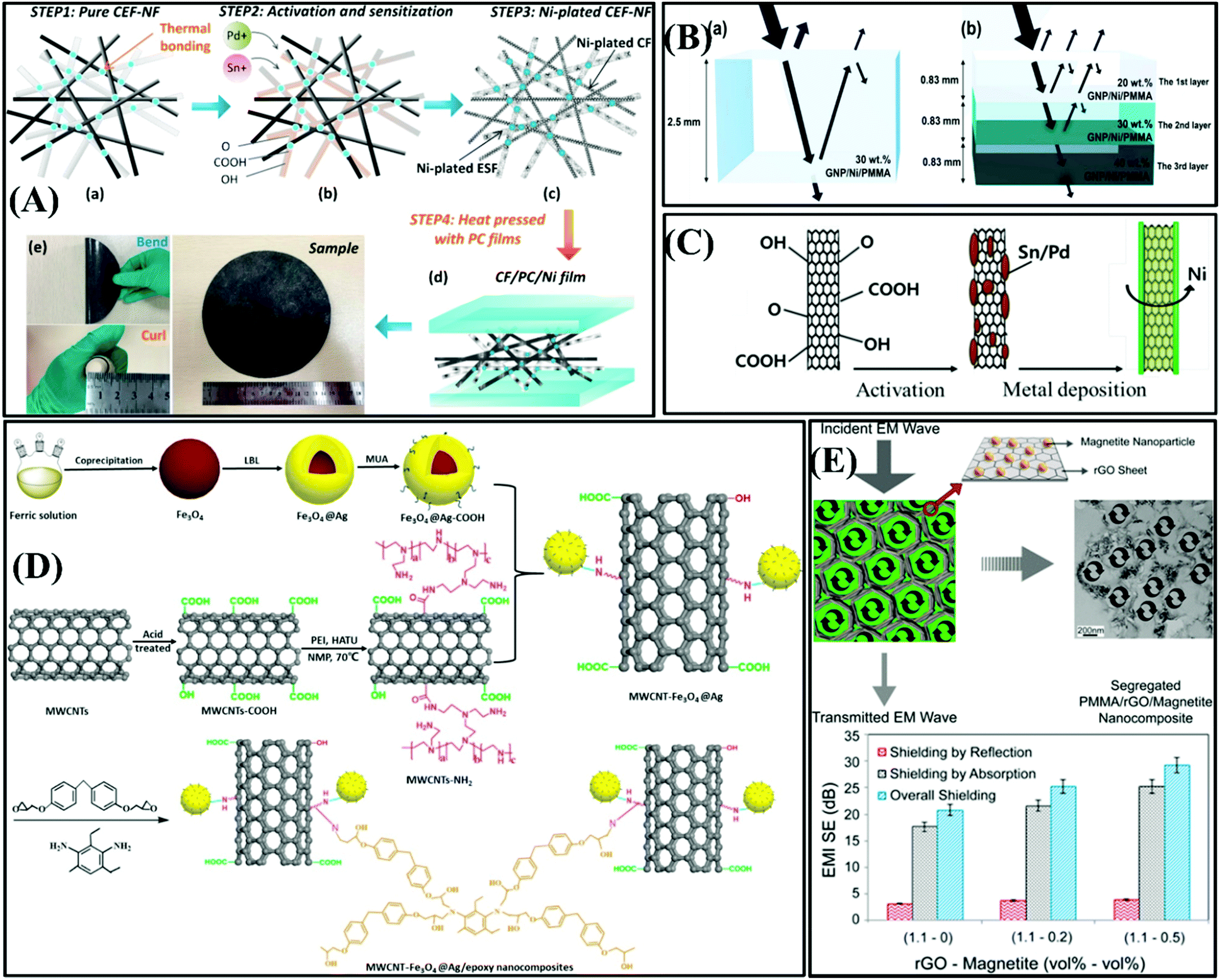 | ||
| Fig. 6 (A) Schematic diagram of the preparation of CF/PC/Ni film.54 Copyright 2018, Elsevier Ltd. (B) Diagram of (a) monolayered GNP/Ni/PMMA nanocomposite and (b) multi-layered GNP/Ni/PMMA nanocomposite.58 Copyright The Royal Society of Chemistry, 2019. (C) Schematic diagram of the electroless Ni-plating processes.59 Copyright 2016, Elsevier Ltd. (D) Flow chart of the preparation process of MWCNT–Fe3O4@Ag/epoxy nanocomposite.60 Copyright 2018, Elsevier Ltd. (E) Fabrication process and EMI shielding characteristics of PMMA/rGO/magnetite nanocomposite.5 Copyright 2017, the American Chemical Society. | ||
Core–shell-structured nickel@graphite nanoplate (Ni@GNP) functional particles were manufactured by Wang et al. using electroless plating technology.55 The EMI test result suggested that the EMI SE of the Ni@GNP film of 57.1 dB is 1.54-times higher than that of the pure GNP film with the same thickness of 0.3 mm in the frequency range of 8.2–12.5 GHz. The Ni@GNP functional composite film exhibited outstanding EM wave absorption ability due to the fact that Ni magnetic metal particles were attached to the surface of GNP, which further enhanced the dielectric loss and magnetic loss. In this experiment, the addition of Ni has three functions. Firstly, the dielectric properties are improved via interfacial electron polarization. Secondly, the presence of a nickel shell improved the magnetic losses. Thirdly, the unique core–shell structure provided an internal multiple reflection conductive network.
To improve the affinity and dispersion between the composite filler and the polymer matrix,56,57 Hye Ji Im et al. prepared multi-layered and monolayered nanocomposites of graphene nanoplatelets (GNP)/Ni/polymethyl methacrylate (PMMA). Nano-Ni particles were uniformly distributed on GNP, and the Ni2+ ions interacted with the functional groups on GNP to form chemical bonds. The GNP/Ni filler exhibited both a high aspect ratio and excellent conductivity, which improved the EMI shielding performance by constructing a conductive network in the polymer matrix. As shown in Fig. 6B, monolayer and multilayer GNP/Ni/PMMA composites were designed with the same average amount of metal (30 wt%) and the same sample thickness (2.5 mm) to simply explore the effect of the multi-layer structure on the shielding performance, and the results showed that the shielding performance of the composite with a multilayer structure increased significantly.58
Carbon nanotubes with a hollow porous structure can provide multiple EM wave reflection networks and further have excellent EMI shielding ability. The added magnetic metal particles and carbon nanotubes can exhibit a synergistic effect to enhance the magnetic loss and dielectric loss. Yoon-Ji Yim et al. fabricated Ni-MWCNT/HDPE composites (Ni-MWCNTs/HDPE) via electroless Ni plating, as shown in Fig. 6C.59 Due to the synergistic effect of the Ni particles and carbon nanotubes, Ni-MWCNT/HDPE presented an excellent EMI SE of 13 dB in the frequency range of 1–1.2 GHz, which is higher than that of 4 dB for MWCNT/HDPE without Ni plating. The traditional method of electroless nickel plating has the disadvantages of great pollution and high cost, and thus researchers have begun to explore new environmentally friendly methods to achieve carbon nanotubes plated with nickel. Wang et al. fabricated MWCNT–Fe3O4@Ag/epoxy nanocomposites via the blending-casting method.60 As shown in Fig. 6D, acidic Fe3O4 and aminated MWCNT were reacted to form MWCNT–Fe3O4@Ag/epoxy nanocomposites via the pouring process. The test results for MWCNT–Fe3O4@Ag/epoxy in terms of electrical conductivity, thermal conductivity, mechanical properties, and thermal properties certified that the MWCNT–Fe3O4/epoxy nanocomposite with MWCNT–Fe3O4@Ag 15 wt% possessed a satisfactory EMI SE of 35 dB, thermal conductivity λ of 0.46 W m−1 K−1 and Young's modulus of 4.60 GPa. The Fe3O4 nanoparticles enhanced the interaction between MWCNT–Fe3O4@Ag and promoted the formation of conductive networks, and meanwhile triggered the hysteresis loss of EM waves, and provided an interface of reflecting and reabsorbing EM waves. The problem of the poor combination of the metal particles and carbon materials was overcome through functionalizing the MWCNTs and acidic Fe3O4 particles, which differs from traditional electroless plating and electroplating methods. Thus, this method opens a way to coat nanoparticles on a substrate with a low surface free energy. Carbonaceous fillers are mainly used to absorb EM waves due to their conductive properties and modifying their structure with magnetic nanoparticles can further improve the efficiency of their electromagnetic interference shielding.56,61 In the study of poly(methyl methacrylate)/reduced graphene oxide/magnetite (PMMA/rGO/Fe3O4) nanocomposites, Sharif et al. prepared a rGO/Fe3O4 composite filler to benefit from both advantages of the segregated structure of rGO and magnetite properties of Fe3O4. As shown in Fig. 6E, the addition of magnetite NPs to the PMMA/rGO nanocomposites improved the EMI SE by increasing the absorption shield, while the reflection shield remained almost unchanged. In addition, when the incident EM wave touches the separated structural layer formed by rGO, the EM wave is absorbed firstly and reflected repeatedly between the internal interfaces until it is completely absorbed and attenuated.5
In summary, researchers have developed many methods, including the fabrication of metal/polymer composites, metal/fabric composites, metal-type transparent composites films, and metal-type aerogels, to solve the defects of easy corrosion, high specific gravity, and insufficient flexibility of traditional metals.
The lightweight and flexible targets of metal can be achieved by coating metal particles on polymer substrates, but it is difficult for polymer interfaces without polar functional groups to combine with metal particles. Due to the presence of a large number of functional groups on its surface, the cellulose fiber matrix is considered an ideal choice as a substrate for metal nanoparticles. Metal-type transparent composite films have been developed towards high transparency, stretchable, and low filling volume. The biggest features of metal-type aerogels are their high shielding effectiveness, positive resilience, ultra-low density, and ultra-high SSE/t. Magnetic metals can improve the permeability and conductivity of composite materials, further enhancing the absorption loss of composites for EM waves. We predict that within the next few years, how to solve the problem of the combination of metal particles and polymers is destined to become a hot issue in the research on metal composite EMI shielding materials. Table 1 presents the EMI shielding properties of metal-type composites.
| Materials | Filler content | Thickness (mm) | Frequency (GHz) | EMI SE (dB) | Ref. |
|---|---|---|---|---|---|
| Notes: PAN: polyacrylonitrile, PP: polypropylene, PDA: polydopamine, PU: polyurethane, NW: nanowire, CNF: carbon fiber fabric, PC: polycarbonate, HDPE: high density polyethylene, GNP: graphene nanoplatelet, PMMA: polymethyl methacrylate, CEF-NF: carbon-fabric, WPU: waterborne polyurethane, and PPy: polypyrrole. | |||||
| PAN nanofiber/Ag | 2 wt% | 0.053 | 8–26.5 | 90 | 42 |
| Textile/Ag/MXene | — | 0.12 | 8–12.5 | 43 | 43 |
| PP/PDA/Ag | 25 wt% | — | 8–12.5 | 70 | 44 |
| PU–Ag NW/CNF/Ag | — | 0.36 | 8–12.5 | 106 | 45 |
| Carbon type fiber/Cu | — | 0.4 | 1.5–10 | 80 | 46 |
| PU/Ag NW | 80 wt% | — | 0.5–3 | 30 | 49 |
| Cu/large graphene | 30 vol% | 0.01 | 1–8 | 35 | 17 |
| Cu and Ag/ITO | — | — | 8–40 | 26 | 53 |
| Cu/Ag NW /PI | — | 0.01 | 0–1.5 | 55 | 47 |
| RGO/Ag NW | — | — | 0.5–3 | 24 | 47 |
| Ag NW/Fe3O4 | — | 0.05 | 8.2–12.5 | 25 | 47 |
| Ag NW@C | — | 0.3 | 8.2–18 | 70 | 16 |
| Cu NW@graphene | — | 0.946 | 8.2–12.5 | 52.5 | 30 |
| Nickel@graphite | — | 0.3 | 8.2–12.5 | 57.1 | 55 |
| Carbon fiber/PC/Ni | — | 0.31 | 0–1.5 | 72.7 | 54 |
| Ni–MWCNTs/HDPE | — | — | 0.5–1.5 | 13 | 59 |
| Fe3O4@Ag/epoxy | 15 wt% | — | 8.2–12.5 | 8 | 60 |
| PC/a-CF/a-CNT | 10.5 wt% | 2 | 10 | 26 | 62 |
| GNP/Ni/PMMA | 30 wt% | 2.5 | 8.2–12.4 | 61 | 58 |
| CEF-NF/Ag/WPU | Ag deposition | 0.183 | 0.03–1.5 | 102.9 | 63 |
| PPy/PDA/AgNW | 50 wt% | — | 8.2–12.4 | 48.4 | 64 |
| PMMA/rGO/Fe3O4 | 2.6 vol% | 2.9 | 8.2–12.4 | 63.2 | 5 |
3.2. Carbon-type shielding materials
Over the years, metals have always been chosen to shield against EM waves. However, due to their inherent characteristics of easy to oxidation and corrosion, it is difficult for metals to maintain their outstanding EMI shielding performances and reliability under extremely harsh conditions, such as humid and acidic environments. Therefore, researchers have turned their attention from metals to carbon-type shielding materials.65–68 Carbon-type materials, including CB,69 CNTs,9 carbon nanofibers (CNFs), and graphene nanosheets,70 have captured the great attention of researchers due to their large aspect ratio, light weight, outstanding mechanical properties, easy processing, and high electrical conductivity.71 As mentioned above, the ability of a material to shield against EM waves is relevant to its intrinsic electrical conductivity. However, most polymers do not have the ability to shield against EM waves because they are insulators. Therefore, it is a useful method to introduce carbon fillers in polymers to obtain higher electrical conductivity and better EMI SE.72,73 In this chapter, we summarize the carbon-type materials used in EMI shielding in recent years.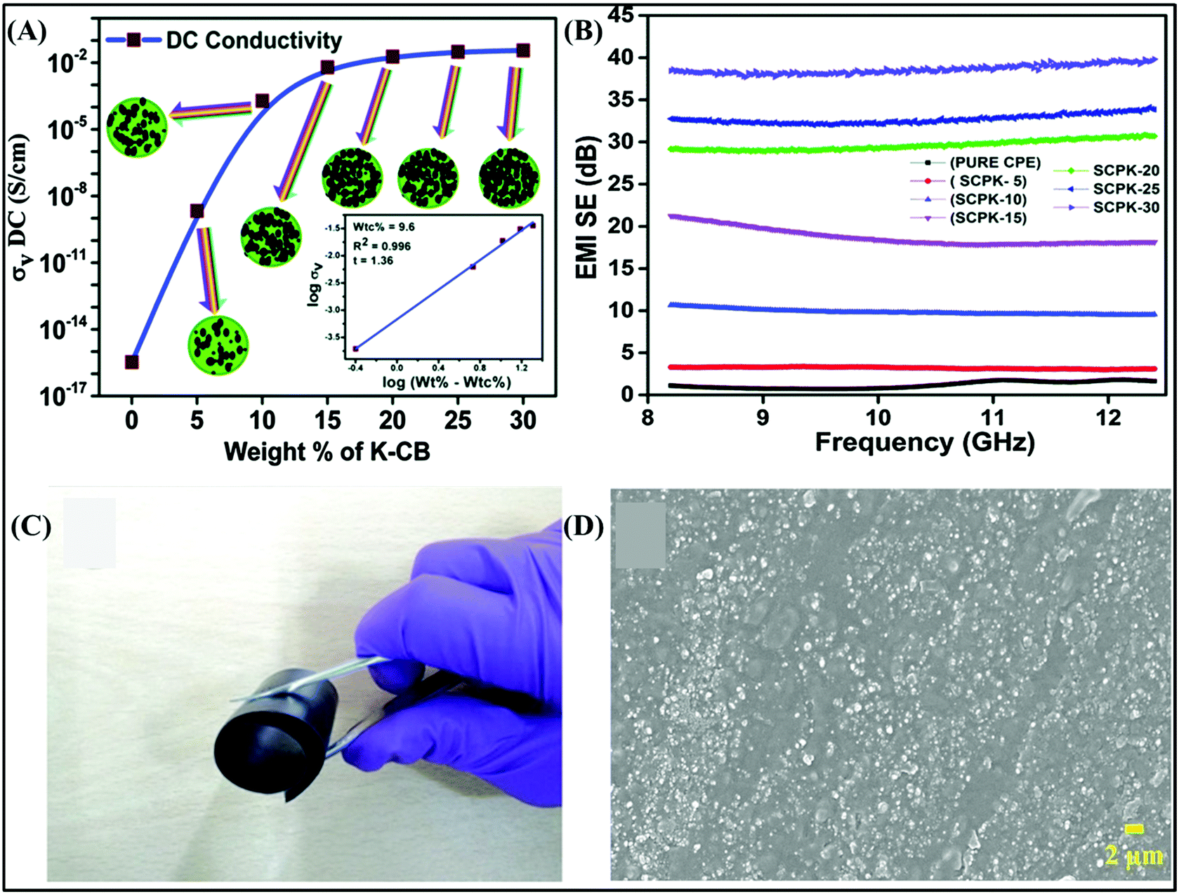 | ||
| Fig. 7 (A and B) DC conductivity and EMI SE of CPE/K-CB composites.69 Copyright 2016, The Royal Society of Chemistry. (C and D) Photograph and SEM image of the highly flexible E50O50V30 specimen.71 Copyright 2018, John Wiley and Sons, Inc. | ||
Generally, adding zero-dimensional CB to the polymer matrix in a certain concentration range can improve the electrical conductivity and EMI shielding performance of composites. However, to achieve satisfactory electrical conductivity and EMI shielding performances, a relatively high filler loading is necessary, which results in the aggregation of the filler and further deteriorates the mechanical properties of the composite. The EMI SE is relevant to not only the CB loading but also the dispersion state of the filler. Therefore, to obtain excellent EMI SE and reduce cost, it is useful to better disperse and distribute the fillers in the polymer matrix. Accordingly, Ravindren et al. demonstrated a structure with an immiscible blend polymer as the matrix and CB as the conductive filler (as shown in Fig. 7C and D). They used ethylene methyl acrylate (EMA) and ethylene octane copolymer (EOC) as the blend polymer to achieve the double penetration phenomenon in the composites, which substantially improved the electrical conductivity and shielding performance due to the selective distribution of CB in the different polymers, and the composites showed an EMI SE of 31.4 dB.71
For example, an EMI shielding composite consisting of SWCNT and polyurethane (PU) was prepared through a simple physical mixing process.81 The EMI SE of the composite material with 20 wt% SWCNT in the X-band was 16–17 dB and the shielding mechanism was mainly ascribed to the reflection of EM waves. The dispersion of CNTs and conductive network of CNTs in the polymer matrix are important for the EMI shielding performance.9,82 Singh et al. used the method of chemical vapor deposition to anchor MWCNTs on carbon fibers, and then used epoxy resin to enhance the mechanical properties of the MWCNT/CF materials. It was found that the EMI SE improved from −21 to −27 dB by incorporating MWCNTs in CF felt.83 Although the high mass ratio of CNTs may enhance the EMI SE, a high loading of CNTs may make is the sample difficult to process due to their severe accumulation.84,85 Thus, to tackle the aggregation of CNTs in polymers, Gong and his co-workers demonstrated a dry spray method for the fabrication of layered CNT/CFRP (carbon fiber reinforced polymer) composites. Consequently, a perfect network was formed in the polymer, significantly promoting the mechanical properties and EMI shielding performance of the composites. The results showed that by adding 2.5 g m−2 CNTs to the interlayer surface, the maximum EMI SE of the CNT/CFRP composites increased from 62 dB to 74 dB.9 In fact, the key factors that limit the mechanical properties, electrical conductivity and EMI shielding effectiveness of CNT films are the interaction between adjacent tubes. Thus, to solve this problem, various methods have been executed for the construction of CNT films, including alignment and mechanical densification, high-temperature epitaxial welding, use of polymer and other conductive materials as a binder, and chemical densification. As shown in Fig. 8A, a highly aligned and compacted CNT film was prepared via the method of floating catalyst chemical vapor deposition and mechanical rolling to achieve high electrical conductivity.76 The CNT bundles were arranged loosely and neatly in the same direction, accompanied by obvious gaps and pores. After further rolling treatment, a denser CNT bundle network was constructed (Fig. 8A). Consequently, this CNT film exhibited enhanced electrical conductivity compared with the film without densification.
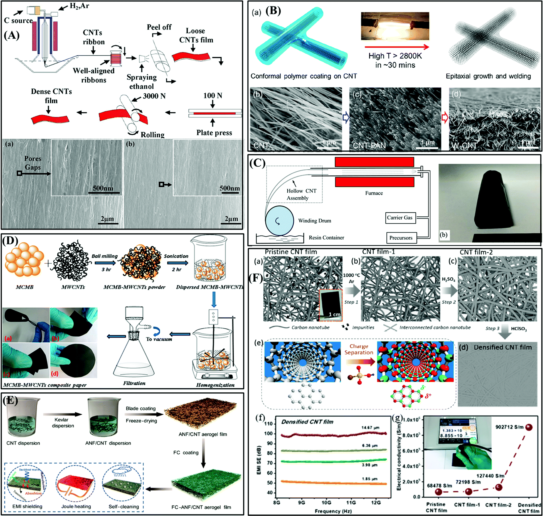 | ||
| Fig. 8 (A) Schematic diagram of the preparation of CNT film and SEM images of the morphology of the CNT film before (a) and after (b) rolling treatment.76 Copyright 2017, Elsevier Ltd. (B) Schematic diagram of W-CNT interconnected by epitaxial welding and SEM image of W-CNT at each step.77 Copyright 2018, the American Chemical Society. (C) Schematic diagram of CNT film assembly process and optical picture of CNT film.78 Copyright 2019, Elsevier Ltd. (D) Fabrication process of MCMB–MWCNT composite paper.79 Copyright 2016, the American Chemical Society. (E) Diagram of the fabrication of FC-ANF/CNT hybrid aerogel film.29 Copyright 2019, the American Chemical Society. (F(a–d)) Outline of the preparation process of densified CNT film. (e) Schematic diagram of the charge separation in a single CNT induced by polar molecules (CSA). (f and g) EMI SE and electrical conductivity of densified CNT film.80 Copyright 2020, the American Chemical Society. | ||
In addition, Yao et al. proposed an “epitaxial welding” strategy to enhance the connection between CNTs and improve the electrical conductivity of CNT films (Fig. 8B).77 Solution-based polyacrylonitrile was coated on CNTs in the form of a “nanogel”, and then the polymer was converted into graphite by high-temperature annealing to produce a network structure, in which the crystal layer acted as a bridge to connect adjacent CNTs. The results revealed that the electrical conductivity and tensile strength of the contact-welded CNTs were 5-times (∼1500 S cm−1) and 20-times higher (∼120 MPa) than that of the unwelded CNT, respectively. As shown in Fig. 8C, CNT impregnation with polymer solution and continuous winding were used to prepare a carbon nanotube (CNT)/polymer composite film that was only 1 mm thick.78 The in situ impregnation of the polymer enhanced the tube–tube interface bond. In addition, Lu et al. reported the preparation of free-standing, flexible, and conductive SWCNT/MWCNT composite films via a spray and vacuum-filtration method.86 This material demonstrated a shielding performance of up to 65 dB and high electrical conductivity of 20000 S m−1 at an areal density of 0.011 g cm−2 and thickness of ∼130 μm. Besides, Chaudhary et al. reported a homogenization and vacuum-assisted filtration method for the preparation of meso-carbon microbead-MWCNT composite paper with the performance of good flexibility, extremely light weight, and high conductivity (Fig. 8D).79 Also, the EMI SE was 31 dB to 56 dB at a thickness of 0.15–0.6 mm.
Recently, Hu et al. fabricated a hydrophobic fluorocarbon (FC) resin-coated ANF/CNT aerogel film via blade coating and freeze-drying (Fig. 8E), which exhibited fascinating properties including robust, thin, light weight, multifunctional, and extra-ordinary EMI SE.29 Its EMI SE was 54.4 dB at the thickness of 568 μm and the SSE was up to 33528.3 dB cm2 g−1. Additionally, the FC coating layer endowed the aerogel film hydrophobicity and self-cleaning performance. In our recent study, an ultrathin densified CNT film was prepared via the purification and densification of a pristine CNT membrane (Fig. 8F(a–e)), where high-temperature and acid treatment removed the impurities, and the charge separation in individual CNTs induced by chlorosulfonic acid led to strong CNT–CNT attraction.80 Consequently, the densified CNT film achieved a remarkable EMI SE of 101 dB at a thickness of 14.7 μm (Fig. 8F(f)) and tensile strength of 822 ± 21 MPa. Meanwhile, these performance of the densified CNT film in harsh environments could be well maintained.
For the first time, Hong reported the EMI shielding performance of single-layer graphene prepared via the CVD method.88 The average SE value of the single-layer CVD graphene was 2.27 dB, which means that about 40% of incident waves can be blocked. Since then, many studies on the EMI shielding performance of multilayer graphene and graphene paper prepared via the CVD method have been reported.89,90 For example, Pradip Kumar provided a detailed overview of pristine graphene materials prepared via the CVD method for EMI shielding.3 In fact, pristine graphene (PG) has higher electrical conductivity (≈106 cm−1) than that of graphene oxide (GO). Thus, it is obvious that PG is an extremely attractive material in the field of EMI shielding due to its high electrical conductivity (≈106 cm−1). Wei et al. used a scalable scanning centrifugal casting method to efficiently prepare highly oriented independent laminated PG films and PG/polymer composite films (as shown in Fig. 9A), which exhibited outstanding EMI shielding performances and excellent mechanical strength.91 The EMI SE of a 100 μm thick PG film could reach 93 dB. The highly oriented PG nanosheets enhanced the tensile strength of the PG film up to about 145 MPa. Although PG has higher electrical conductivity than that of GO, it is difficult to prepare polymer composites with a homogenous dispersion of PG due to its chemical inertness. In this context, GO with abundant oxygen-containing functional groups is a more suitable precursor for graphene-based composites owing to its good dispersion in water and polar organic solvents. Therefore, many studies have used GO instead of PG to prepare graphene-based EMI shielding materials. The restacked and aggregated graphene in the polymer matrix will deteriorate the performance of composites such as their mechanical properties.72,92
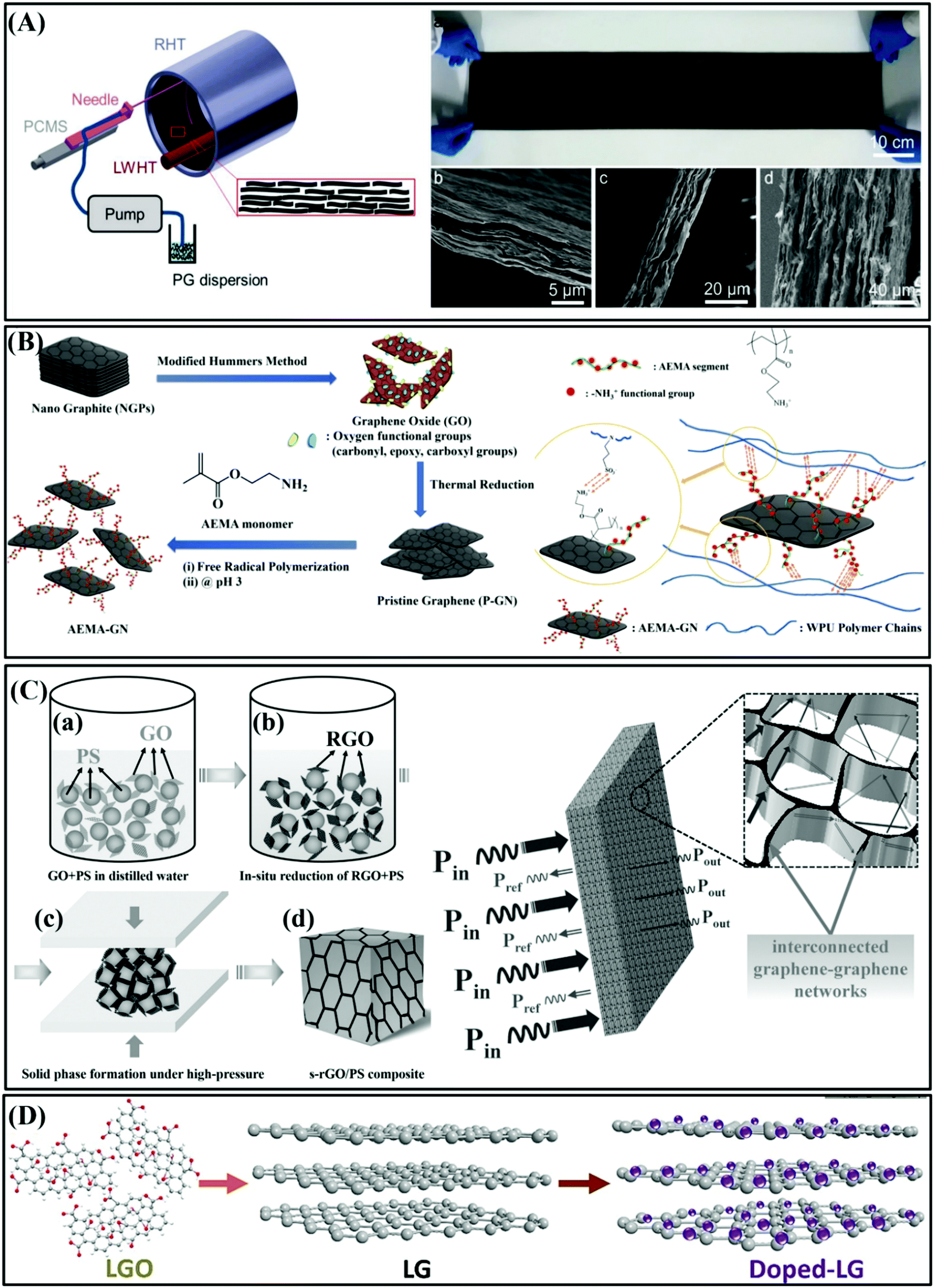 | ||
| Fig. 9 (A) Diagram of the manufacture of PG film with SCC and EMI SE of PG film.91 Copyright 2021, John Wiley and Sons, Inc. (B) Process flow chart of manufacturing P-GN and AEMA–GN.70 Copyright 2015, the American Chemical Society. (C) Flow chart of the synthesis of segregated rGO/PS (s-rGO/PS) composite.93 Copyright 2014, Wiley-VCH Verlag GmbH and Co. KGaA, Weinheim. (D) Schematic illustration of iodine-doped large-sized graphene film.94 Copyright 2017, Elsevier Ltd. | ||
Thus, to overcome this disadvantage, a lot of technologies to improve the dispersion stability of graphene fillers have been studied, where one of the effective methods is covalent modification of graphene nanosheets. For example, Hsiao et al. prepared graphene nanosheet (GN)/waterborne polyurethane (WPU) composites with good electrical conductivity and high EMI SE.70 The GN/WPU composites were prepared via covalent modification with aminoethyl methacrylate (AEMA) using free radical polymerization. The covalently modified AEMA–GN segment grafting the organic functional group AEMA to the surface of GN is positively charged (–NH3+), which helps to uniformly disperse GNs in aqueous solution and prevent their stacking. In contrast, the WPU chain end is negatively charged (–SO3−), and the strong interaction between AEMA–GN and WPU causes AEMA–GN to be uniformly and stably dispersed in the WPU matrix, which is beneficial for the formation of a GN conductive network (as shown in Fig. 9B). Consequently, the GN/WPU composites exhibited an EMI SE of 38 dB in the X-band (8.2–12.4 GHz).70
Another important method is the creation of a segregated structure, which can reduce the percolation threshold and increase the electrical conductivity. Yan et al. combined a segregated architecture with high-pressure solid-phase compression molding to produce reduced graphene oxide (rGO) and polystyrene (PS) composites for efficient EMI shielding (as shown in Fig. 9C).93 The segregated architecture with only 3.47 vol% rGO showed an EMI SE of 45.1 dB. The conductive networks were formed due to the distribution of rGO at the interfaces of the PS multi-facets instead of its homogeneous distribution throughout the polymer matrix. The above-mentioned work mainly focused on studying the EMI shielding performance of graphene films and graphene-based polymer composites. However, it has been reported that large-size graphene sheets with fewer defects have higher electrical conductivity and better mechanical properties.95 Nevertheless, the lower carrier density of graphene hinders the further improvement of its electrical conductivity and EMI shielding performance.96 Thus, doping an electron acceptor or donor is an effective method to increase the carrier density of the material. In our previous work, we doped iodine in large-size graphene sheets to increase the carrier density of the graphene nanosheets (the preparation process is shown in Fig. 9D) and studied the effect of the size of graphene nanosheets and the surface doping with iodine on the EMI shielding performance.94 The iodine-doped large-size graphene film exhibited an EMI SE of up to 52.2 dB without compromising the mechanical properties of the graphene film.
For example, Chen et al. reported light-weight and high-performance epoxy/3D CNT sponge composites with excellent EMI shielding properties.84 Firstly, 3D CNT foam was synthesized via the chemical vapor deposition method and adopted as a conductive skeleton for the EMI shielding materials owing to its extraordinary properties, including freestanding shape, great mechanical properties, and high porosity. Then, they used a template-free method to synthesize the epoxy/3D carbon nanotube sponge composites via the infiltration of 3D carbon nanotube sponge. The EMI SE of the epoxy nanocomposite with 0.66 wt% of CNT sponge was around 33 dB (as shown in Fig. 10A). Moreover, this EMI SE is higher than that obtained with 20 wt% of conventional CNTs. It can be seen from Fig. 10A that only 0.66 wt% of carbon nanotube sponge could significantly improve the tensile strength of the material. Additionally, the influence of hole shape or hole orientation in the hole structure on EMI SE was first studied by Zeng et al. They used the freeze-drying method to create a multi-walled carbon nanotube (MWCNT)/water-based polyurethane (WPU) composite material, which has the characteristics of flexibility, anisotropy, and porosity.99 Compared with pure WPU or CNT, the addition of polymer improved the mechanical properties of the material (as shown in Fig. 10B). The results demonstrated that by adjusting the ratio of the electric MWCNT, WPU matrix, and porosity, the EMI SE could be controlled in a wide range (as shown in Fig. 10B).
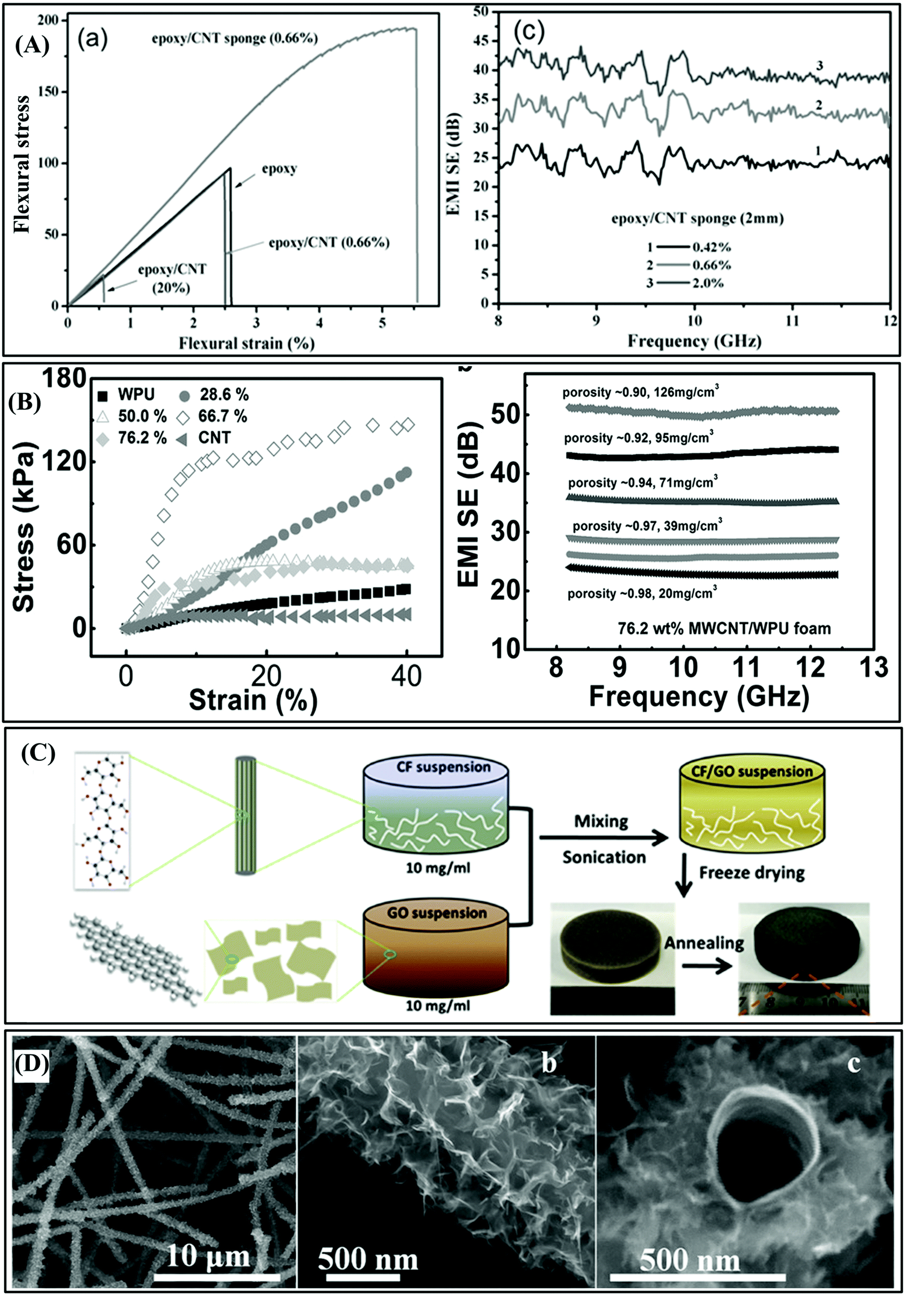 | ||
| Fig. 10 (A) Flexural properties and EMI SE of epoxy/CNT sponge.84 Copyright 2015, John Wiley and Sons, Inc. (B) Optical image of porous MWCNT/WPU composite material, SEM image, mechanical properties, and EMI SE of anisotropic porous structure composite material.99 Copyright 2015, John Wiley and Sons, Inc. (C) Schematic diagram of the manufacturing process of hybrid aerogel.100 Copyright 2017, Elsevier Ltd. (D) Process of the fabrication of the CNT–MLGEP core–shell hybrid foam.33 Copyright 2017, John Wiley and Sons, Inc. | ||
In addition to CNTs being used to prepare 3D materials, graphene is also used to prepare 3D composite materials for shielding EM waves. For example, Chen et al. studied a method for the synthesis of graphene/PDMS foam composites with high electrical conductivity and effective EMI SE without the foaming process.85 In addition to the 3D sponge and foam structures described above, 3D graphene aerogels have also attracted the interest of researchers. Our group synthesized graphene aerogel–epoxy composites (GA–EP) by adding epoxy resin to a 3D graphene aerogel and then curing it.26 The effects of small and large-sized graphene oxide sheets on the composite materials were also studied. The experimental results showed that the EMI shielding performance of the GA–EP composites is better than that of small-size GA–EP. There is a good three-dimensional conductive network inside the 3D graphene aerogel, and thus it exhibited outstanding electrical conductivity and high porosity. The EMI SE of large-size GA–EP at a thickness of 3 mm and 1.0 wt% filler is about 30 dB in the frequency range of 10–20 GHz.
Moreover, in addition to the above-mentioned method of using epoxy and PDMS as curing agents to toughen the mechanical properties of carbon-type composites, freeze-drying is also a commonly used method for the preparation of three-dimensional structural materials. We prepared a CF/RGO hybrid aerogel with outstanding EMI SE through the method of simple solution mixing, freeze-drying, and annealing reduction (preparation process is shown in Fig. 10C). In addition, the CF/RGO hybrid aerogel has the advantage of super-elasticity and compression stability. This super-elastic and porous CF/RGO hybrid aerogel exhibited an EMI SE of 47.8 dB at 18 GHz when its thickness was 5 mm, its EMI SE could be adjusted by mechanical compression.100
Sahoo et al. reported the preparation of 3D graphene/noble metal (Pt and Ag) nanocomposites via an ice template and freeze-drying method. The as-obtained 3D-graphene/noble metal nanocomposites exhibited an excellent EMI of around 28 dB in the X-band (8.2–12.4 GHz) and great elasticity and outstanding electrical conductivity.102 In another work, CNT-multi-layered graphene edge plane (MLGEP) core–shell foam was fabricated via chemical vapor deposition (CVD) (Fig. 10D).33 The composite material of CNT–MLGEP, where MLGEPs seamlessly grew on CNTs via covalent bonding, exhibited the full advantages of both nanocarbons. The as-synthesized CNT–MLGEP core–shell hybrid foam showed excellent EMI shielding of 47.5 dB at a thickness of 1.6 mm. By controlling the PECVD time, the density of the CNT–MLGEP foam could be adjusted. In general, three-dimensional carbon-type shielding materials exhibit excellent characteristics such as low density, lightness, and excellent shielding performance. It has also been shown that the combination of material and structure can achieve ideal performances. Table 2 lists some of the recent carbon-type composites for EMI shielding.
| Materials | Filler content | Thickness (mm) | Frequency (GHz) | EMI SE (dB) | Ref. |
|---|---|---|---|---|---|
| Notes: CPE: chlorinated polyethylene, EMA: ethylene methyl acrylate, EOC: ethylene octane copolymer, PU: polyurethane, CF: carbon fiber, CFRP: carbon fiber-reinforced polymer, ANF: aramid nanofiber, PG: pristine graphene, MCMs: meso-carbon microbeads, GN: graphene nanosheet, WPU: water-based polyurethane, PS: polystyrene, PDMS: polydimethylsiloxane, GA–EP: graphene aerogel–epoxy composites, and MLGEP: multilayered graphene edge plane. | |||||
| (CPE)–K-CB | 30 wt% | 1 | 8.2–12.4 | 38.4 | 69 |
| EMA/EOC/VCB | 30 wt% | 2 | 8.2–12.4 | 31.4 | 71 |
| SWCNT/MWCNT film | 30 wt% | 0.13 | 8.2–12.4 | 65 | 86 |
| Densified CNT film | Bulk | 0.0147 | 8.2–12.4 | 101 | 80 |
| PU/SWCNT | 20 wt% | — | 8.2–12.4 | 16–17 | 81 |
| MWCNT/CF/epoxy | — | 2.5 | 12.4–18 | 21–27 | 83 |
| Layered CNT/CFRP | 2.5 g m−2 | — | 8.2–12.4 | 74 | 9 |
| MCMs–MWCNT composite paper | 25 wt% | 0.6 | 8.2–12.4 | 56 | 79 |
| ANF/CNT aerogel film | 40 wt% | 0.568 | 8.2–12.4 | 54.4 | 29 |
| Laminated PG film | Bulk | 0.1 | 8.2–12.4 | 93 | 91 |
| GN/WPU | 5 vol% | — | 8.2–12.4 | 38 | 70 |
| rGO/PS | 3.47 vol% | 2.5 | 8.2–12.4 | 45.1 | 93 |
| r-GO/SiO2 | 20 wt% | 1.5 | 8.2–12.4 | 38 | 101 |
| Iodine-doped graphene film | Bulk | 0.0125 | 8.2–12.4 | 52.2 | 94 |
| CNT/epoxy sponge | 0.66 wt% | 2 | 8.2–12.4 | 33 | 84 |
| MWCNT/WPU | 2.2 vol% | 4.5 | 8.2–12.4 | 49.2 | 99 |
| Graphene/PDMS foam | 0.8 wt% | 1 | 0.03–1.5 | ∼30 | 85 |
| GA–EP | 1.0 wt% | 3 | 10–20 | 30 | 26 |
| CF/RGO hybrid aerogel | 77 wt% | 5 | 11.9–18 | 47.8 | 100 |
| 3D-graphene/metal | — | 0.8 | 8.2–12.4 | 28 | 102 |
| CNT–MLGEP core–shell foam | — | 1.6 | 8.2–12.4 | 47.5 | 33 |
3.3. MXene-type shielding materials
MXenes, as 2D early transition metal carbides/nitrides, are regarded as EMI shielding material owing to their good hydrophilicity, excellent electrical conductivity, and large specific surface area.103–105 Typically represented by Ti3C2Tx, MXenes have been used to construct a series of MXene-type EMI shielding materials, including films, fabrics, foams, and aerogels.3 This chapter summarizes the MXene-type materials used in EMI shielding in recent years.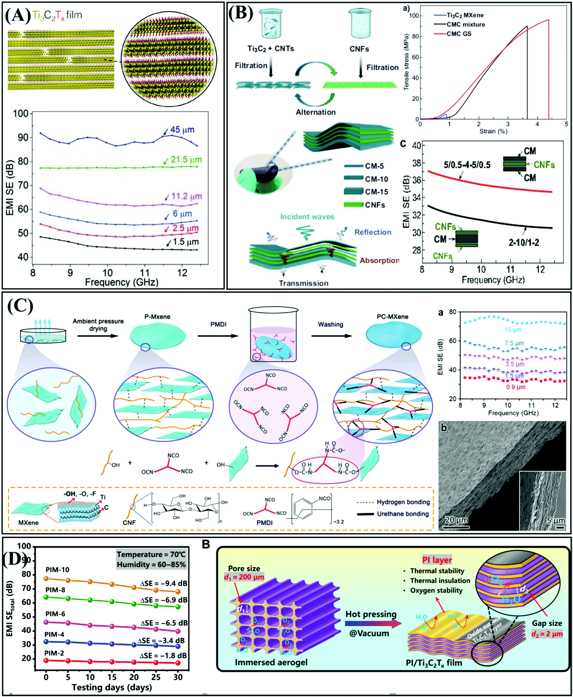 | ||
| Fig. 11 (A) Ti3C2Tx film with excellent EMI SE of 92 dB at a thickness of 45 μm.24 Copyright 2016 American Association for the Advancement of Science. (B) Carbon nanotube/Ti3C2 MXene/CNF composite films with gradient and sandwich structure.106 Copyright Springer Nature. (C) Schematic of the preparation of PC–MXene.107 Copyright 2021, John Wiley and Sons, Inc. (D) EMI SE of PI/Ti3C2Tx films treated under hygrothermal conditions and schematic diagram of the protective effect of PI.108 Copyright 2021, American Association for the Advancement of Science. | ||
Recently, Wu et al. report the preparation of a PC–MXene film via the physical and chemical double cross-linking of CNFs and MXene nanosheets (Fig. 11C).107 Compared with the MXene film, the PC–MXene film showed significantly improved mechanical strength without compromising the excellent EMI SE. In addition, the PC–MXene film exhibited a high SE of 33.3 dB at a thickness of only 0.9 μm, which is unattainable for pure MXene films. In addition to their poor mechanical properties, easy oxidation is also a fatal flaw of MXenes. Chen et al. prepared a layered porous polyimide (PI)/Ti3C2Tx film with continuous conductive paths.108 This film not only exhibited high electrical conductivity and shielding performance, but also maintained an excellent EMI shielding performance under harsh conditions such as hygrothermal or combustion environments, low temperature (−196 °C) or high temperature (250 °C) and rapid thermal shock (ΔT = 446 °C). The mechanical properties and oxidation stability of MXene are still the focus of urgent research.
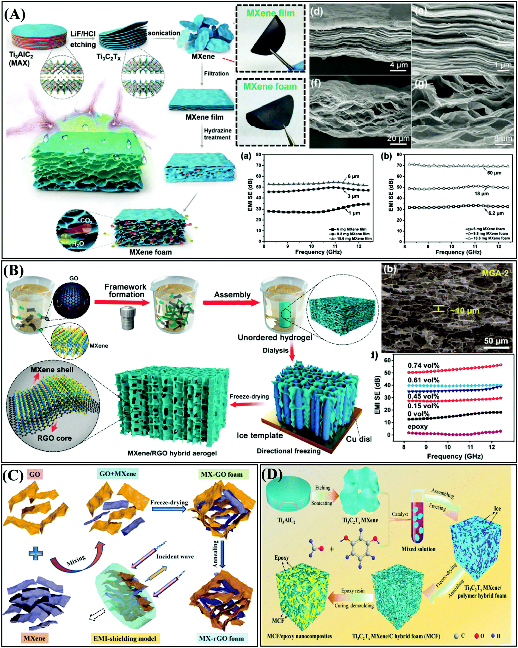 | ||
| Fig. 12 (A) Schematic illustration of the fabrication, SEM image, and EMI SE of the hydrophobic and flexible MXene foam.114 Copyright 2017, John Wiley and Sons, Inc. (B) Schematic illustration of the fabrication, SEM image, and EMI SE of MXene/RGO aerogel.115 Copyright 2018, the American Chemical Society. (C) Ti3C2Tx MXene/graphene hybrid foam with 3D porous architecture.116 Copyright 2019, Elsevier B.V. (D) Ti3C2Tx MXene/C hybrid foam/epoxy nanocomposite with 3D porous architecture.117 Copyright 2019, Elsevier Ltd. | ||
Fan et al. fabricated a lightweight and conductive MXene/graphene hybrid foam via freeze-drying and heat treatment for superior EMI shielding performance (Fig. 12C).116 The porous MX–rGO foams were characterized by high electrical conductivity and low density. The incident EM waves were rapidly absorbed or attenuated by multiple internal reflections and scattering in the interconnected porous conductive network of the MX–rGO foam. Wang et al. prepared a three-dimensional Ti3C2Tx MXene/C hybrid foam (MCF)/epoxy nanocomposite via a series of methods, including sol–gel method, thermal reduction, vacuum-assisted impregnation and epoxy curing.117 Conductive MXene nanosheets were evenly distributed in the 3D cross-linking network to construct a complete and efficient conductive pathway. As shown in Fig. 12D, the as-prepared MCF/epoxy nanocomposite (5 wt% MXene) exhibited the optimum electrical conductivity of 184 S m−1 and the maximum EMI SE of 46 dB. The unique three-dimensional porous architectures can expand the application of the MXene-type composites in the field of EMI shielding. Table 3 shows the EMI shielding properties of MXene-type composites.
| Materials | Filler content | Thickness (mm) | Frequency (GHz) | EMI SE (dB) | Ref. |
|---|---|---|---|---|---|
| Notes: TOCNF: 2,2,6,6-tetramethyl-1-piperidinyloxy (TEMPO) oxidized cellulose nanofiber. CMC GS: CNTs/MXene/CNFs composite film with gradient and sandwich structure. PC–MXene: physical and chemical dual cross-linking of MXene. PI: polyimide. | |||||
| Ti3C2Tx film | Bulk | 0.045 | 8.2–12.4 | 92 | 24 |
| d-Ti3C2Tx/CNF | 80 wt% | 0.047 | 8.2–12.4 | 25.8 | 111 |
| Ti3C2Tx/TOCNF | 50 wt% | 0.038 | 8.2–12.4 | 39.6 | 4 |
| CMC GS | 80 wt% | 0.038 | 8.2–12.4 | 38.4 | 106 |
| CNF/MXene | 50 wt% | 0.035 | 8.2–12.4 | 40 | 112 |
| PC–MXene film | 50 wt% | 0.0009 | 8.2–12.4 | 33.3 | 107 |
| PI/Ti3C2Tx film | 2 vol% | 0.21 | 8.2–12.4 | 77.4 | 108 |
| MXene foam | Bulk | — | 8.2–12.4 | 70 | 114 |
| 3D MXene/RGO aerogel | 0.74 vol% | — | 8.2–12.4 | 50 | 115 |
| MXene–rGO foam | Bulk | 3 | 8.2–12.4 | 50.7 | 116 |
| Ti3C2Tx MXene/C | 4.25 wt% | 2 | 8.2–12.4 | 46 | 117 |
4. Near-field shielding
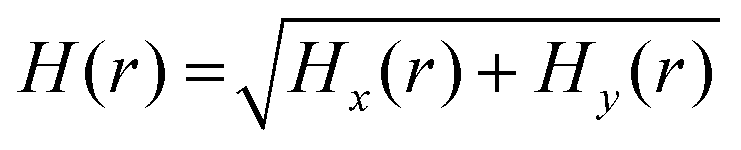
Considering the distance between the radiation source and the shielding material, radiation can be divided into near-field radiation (kr ≪ 1) and far-field radiation (kr ≫ 1), where k is the wavenumber and r is the distance from the EM source to the detector. In the far-field region, EM waves can be regarded as plane waves, where the wave impedance (electric field/magnetic field) is constant, and the SEE (SE of the electric field) is equal to the SEM (SE of the magnetic field). Different from the far-field region, the SEE and SEM of the near-field are inconsistent and can vary with the distance from the source.118 Therefore, it is necessary to measure the values of SEE and SEM in the near field separately. At present, there are two test methods for near-field electric and magnetic shielding. In the first method, the near-field electric and magnetic measurements are performed on shielding materials coated on a test board.119,120 For the near-field electric shielding measurement, firstly, a patch source pattern is used to generate electric fields. Secondly, a strip-line is used to measure near-field electric leakage from the shielding material. Then, the SE of shielding materials can be obtained from the 3-port S-parameter of the VNA. For near-field magnetic shielding measurement, firstly, a microstrip line source with a 50 Ω load is used to generate a magnetic field. Secondly, a loop-probe is used to capture near-field magnetic leakage from the shielding material. Similarly, the SE can be extracted from the 2-port S-parameter of the VNA. The second method is to use a near-field scanning measurement setup (as shown in Fig. 13A), which is more flexible compared to the traditional method.121 The near-field scanning platform includes a computer for controlling the system, a robotic arm, which is used to fix the probe, a magnetic probe (the magnetic probe can be replaced by an electric probe to measure the electric field) to detect the magnetic field radiated from the SiP (System-in-package), and spectrum analyzers (used to measure the active devices) or vector network analyzers as receivers. According to the different probes, the radiation value of different frequency bands can be measured. The near-field SE is defined as follows:| SENF = 20log10|Hunshielded(r)/Hshielded(r)| | (17) |
 | (18) |
 | ||
| Fig. 13 (A) Near-field scanning measurement platform. (B) Results of without shielding materials and with shielding materials.124 Copyright 2021, Elsevier Ltd. | ||
SiP is essential for the miniaturization and multi-function of electronic equipment; however, the complex EM wave radiation from SiP can cause serious EMI problems.122 Therefore, the problem of EMI between different components in SiP needs to be solved urgently. Accordingly, conformal shielding has already substituted the traditional metal shielding cover.123 Given the small size and weak radiation of SiP, traditional SE measurement methods, such as anechoic chambers and reverberation chambers, are not suitable for measuring its EMI SE. In practical applications, to determine the EMI SE of shielding SiP, researchers have adopted EM near-field scanning technology. For example, Vikas Rathi et al. prepared a conductive composite sheet and investigated the EMI SE in the near-field and far-field regions. Moreover, Lin et al. analyzed the SE of magnetic materials in the near- and far-field and studied the effects of using magnetic materials in a wireless charging coil module.125 Jog et al. measured the near-field radiation from a car deck player and found that the microcontroller, crystal oscillator, and coil on the PCB generated the maximum radiation.126 Subsequently, Shen et al. demonstrated the use of shielding materials to reduce the EM radiation of a chip.124 The result shows that the shielding materials can effectively reduce EMI. With the highly integrated trend of SiP, shielding materials will be used to effectively shield EMI sources in the near-field and far-field regions.
5. Conclusions and outlook
In this review, we highlighted the recent research progress in various EMI shielding materials including metal-type materials, carbon-type materials, and MXene-type materials. We mainly focused on the effect of their electrical conductivity, and structure of composites on their EMI shielding performance. The corresponding shielding mechanism was analyzed to elucidate the structural design principles of shielding materials. Although metal-type, carbon-type, and MXene-type materials have made significant achievements in the field of EMI shielding, there are still many issues to be explored for practical EMI shielding applications. Accordingly, we hope to provide guidelines to advance the design of EMI shielding materials for further research. It is expected that the following future research directions will be developed soon.(1) In the previous part of this article, we introduced EMI shielding with different structures, concluding with layered, foam, and isolated structures. The development of EMI shielding materials with novel structures may be a research direction. For example, Shen et al. constructed strong flexible polymer/graphene composite films with 3D saw-tooth folding for enhanced and tunable EMI shielding.127 The change in the folded angle and side length will cause changes in the shielding performance of the material, so that the material performance can be adjusted through simple mechanical deformation, which is shown in Fig. 14A. However, for materials with good electrical conductivity, it is difficult to balance good interfacial impedance matching and strong dielectric loss. Therefore, optimizing the structure and components to obtain better EMI shielding performances may be a research direction. For example, Sun et al. adjust the impedance matching by designing the structure of materials to obtain better electromagnetic absorption performances.128
 | ||
| Fig. 14 EMI shielding materials with specific macro-structures: (A) polyurethane/graphene composites with saw-tooth folding structure.127 Copyright 2016, Elsevier Ltd. (B) Diagram of the manufacturing process of smart contact lenses with graphene coating.129 Copyright 2017, the American Chemical Society. (C) EMI SE of Ti3CNTx and Ti3C2Tx films and cross-sectional TEM images of Ti3CNTx films at 350 °C.130 Copyright 2020, American Association for the Advancement of Science. (D) Preparation, SEM image, and EMI SE characterization of TaSe3 polymer insulating composite films.131 Copyright 2021, John Wiley and Sons, Inc. | ||
(2) Additionally, the development of new application scenarios for EMI shielding materials may be a research point. For example, graphene-coated contact lenses protect the eyes from EM waves compared with ordinary contact lenses (Fig. 14B).129 If graphene-coated contact lens is used, the electromagnetic energy is absorbed by graphene and dissipates as heat before reaching the inside of the eye. Although graphene is widely used in the research on EMI shielding materials, it is a very novel idea to use it as a coating for smart contact lenses through special processing processes.
(3) Ti3C2Tx, as the most conductive material in the MXene family, has been widely explored for use in the field of EMI shielding. Even though the reflection and absorption of EM waves can be controlled by designing the structure of MXene materials, the overall EMI SE has not been substantially improved. Later, Aamir Iqbal et al. demonstrated the transition metal carbonitride Ti3CNTx MXene and studied its EMI shielding ability.130 As is known, high-efficiency EMI shielding materials generally have high electrical conductivity. The synthesized Ti3CNTx had low electrical conductivity, and its EMI SE was lower than that of Ti3C2Tx. However, surprisingly, after heat treatment at 350 °C, the Ti3CNTx film showed an EMI SE of 116 dB, which is greater than the 93 dB measured for the annealed Ti3C2Tx. This abnormal phenomenon may be due to the abnormally high absorption of EM waves in the layered structure (as shown in Fig. 14C). These abnormal phenomena provide a wider range of research ideas for studying MXene materials.
(4) As is known, excellent electrical conductivity is a prerequisite for high EMI shielding effectiveness. However, to our surprise, an insulating polymer film with excellent EMI shielding properties was reported by Zahra Barani et al. As shown in Fig. 14D, they used TaSe3, a quasi 1D van der Waals material, as a filler and compounded with a polymer to prepare a polymer composite film.131 TaSe3, a transition metal trihalide with a one-dimensional structure motif, could be exfoliated into atomic beams with an ultra-high aspect ratio of up to 106 after treatment. The experimental results indicated that the polymer composite material with <3 vol% quasi 1D TaSe3 filler exhibited insulating properties, while exhibiting an excellent EMI shielding performance in the X-band GHz and extremely high sub-THz frequency range. This article indicates that the unique EMI shielding properties of these insulating films are derived from the fact that EM waves can effectively couple with free electrons on the TaSe3 atomic filament. These novel films provide a new direction for the preparation of more insulating EMI shielding films for high-frequency communication technology.
(5) Most of the existing EMI shielding materials can effectively attenuate EM waves mainly through reflection, which leads secondary EM pollution. For example, the metal-type, carbon-type, and MXene-type materials exhibit outstanding EMI shielding performances due to their excellent electrical conductivity and structure. Therefore, EMI shielding materials with low-reflection and high-absorption still need to be further explored.
(6) Additionally, some efforts have been focused on developing multifunctional EMI shielding materials at the present stage. For instance, the FC/ANF/CNT aerogel film exhibited the properties of outstanding EMI shielding, Joule heating and self-cleaning. The development of multifunctional materials that combine EMI shielding performance with other functions such as anticorrosion, good heat dissipation and hydrophobicity is a direction worth exploring.
(7) The controllable preparation of two-dimensional nanomaterials and the design of various structures are the key to the development of EMI shielding materials. As mentioned above, MXenes demonstrated remarkable electrical conductivity and excellent EMI shielding efficiency. Moreover, MXene nanosheets are easy to process due to the abundant functional groups on their surface, but their stability is poor and they are easily oxidized. Besides, the force between MXene nanosheets is too weak to form a strong structure. Therefore, new methods for the preparation and anti-oxidation of MXene, as well as the design of the structure of materials urgently need to be developed.
(8) Although the research on EMI shielding materials is very extensive, the underlying mechanism of how shielding materials interact with EM waves is still poorly understood. Thus, it is a development direction to study the EMI shielding mechanism with the aid of simulation software such as HFSS, CST and COMSOL.
Conflicts of interest
There are no conflicts to declare.Acknowledgements
This work was supported by Foundation and Applied Basic Research Fund project of Guangdong Province (2019A1515111034), Shenzhen basic research plan (JCYJ20190807154409372), the Shenzhen Post-doctoral Funding (E19106), and National Natural Science Foundation of China (Grant 52103090).References
- K. Raagulan, B. M. Kim and K. Y. Chai, Nanomaterials, 2020, 10(4), 702 CrossRef CAS PubMed.
- H. Wei, Z. Zhang, G. Hussain, L. Zhou, Q. Li and K. Ostrikov, Appl. Mater. Today, 2020, 19, 100596 CrossRef.
- P. Kumar, Adv. Mater. Interfaces, 2019, 6(24), 1901454 CrossRef.
- Z. Zhan, Q. Song, Z. Zhou and C. Lu, J. Mater. Chem. C, 2019, 7, 9820–9829 RSC.
- F. Sharif, M. Arjmand, A. A. Moud, U. Sundararaj and E. P. L. Roberts, ACS Appl. Mater. Interfaces, 2017, 9(16), 14171–14179 CrossRef CAS.
- J. Huo, L. Wang and H. Yu, Mater. Sci., 2009, 44(15), 3917–3927 CAS.
- M. H. Al-Saleh and U. Sundararaj, Carbon, 2009, 47(7), 1738–1746 CrossRef CAS.
- J. R. N. Gnidakouong, M. Kim, H. W. Park, Y. B. Park, H. S. Jeong, Y. B. Jung, S. K. Ahn, K. Han and J. M. Park, Composites, Part A, 2013, 50, 73–80 CrossRef CAS.
- S. Gong, Z. H. Zhu, M. Arjmand, U. Sundararaj, J. T. W. Yeow and W. Zheng, Polym. Compos., 2018, 39(S2), E655–E663 CrossRef CAS.
- Z. P. Chen, C. Xu, C. Q. Ma, W. C. Ren and H. M. Cheng, Adv. Mater., 2013, 25(9), 1296–1300 CrossRef CAS PubMed.
- X. Y. Sun, X. Liu, X. Shen, Y. Wu, Z. Y. Wang and J. K. Kim, Composites, Part A, 2016, 85, 199–206 CrossRef CAS.
- Y. Wu, Z. Y. Wang, X. Liu, X. Shen, Q. B. Zheng, Q. Xue and J. K. Kim, ACS Appl. Mater. Interfaces, 2017, 9(10), 9059–9069 CrossRef CAS.
- X. Zhang, H. H. Wang, R. Hu, C. Y. Huang, W. J. Zhong, L. M. Pan, Y. B. Feng, T. Qiu, C. F. Zhang and J. Yang, Appl. Surf. Sci., 2019, 484, 383–391 CrossRef CAS.
- C. Liang, Z. Gu, Y. Zhang, Z. Ma, H. Qiu and J. Gu, Nano-Micro Lett., 2021, 13, 181 CrossRef CAS PubMed.
- A. K. Singh, A. Shishkin, T. Koppel and N. Gupta, Composites, Part B, 2018, 149, 188–197 CrossRef CAS.
- Y. J. Wan, P. L. Zhu, S. H. Yu, R. Sun, C. P. Wong and W. H. Liao, Small, 2018, 14(27), e1800534 CrossRef PubMed.
- Z. Wang, B. Mao, Q. Wang, J. Yu, J. Dai, R. Song, Z. Pu, D. He, Z. Wu and S. Mu, Small, 2018, 14(20), e1704332 CrossRef.
- Y.-J. Wan, X.-M. Li, P.-L. Zhu, R. Sun, C.-P. Wong and W.-H. Liao, Composites, Part A, 2020, 130, 105764 CrossRef CAS.
- E. T. Thostenson and T. W. Chou, Composites, Part A, 1999, 30(9), 1055–1071 CrossRef.
- D. E. Clark, D. C. Folz and J. K. West, Mater. Sci. Eng., A, 2000, 287(2), 153–158 CrossRef.
- S. Das, A. K. Mukhopadhyay, S. Datta and D. Basu, Bull. Mater. Sci., 2008, 31(7), 943–956 CrossRef CAS.
- Z. Wu, K. Pei, L. Xing, X. Yu, W. You and R. Che, Adv. Funct. Mater., 2019, 29(28), 1901448 CrossRef.
- K. Rajavel, S. Luo, Y. Wan, X. Yu, Y. Hu, P. Zhu, R. Sun and C. Wong, Composites, Part A, 2020, 129, 105693 CrossRef CAS.
- F. Shahzad, M. Alhabeb, C. B. Hatter, B. Anasori, S. Man Hong, C. M. Koo and Y. Gogotsi, Science, 2016, 353(6304), 1137–1140 CrossRef CAS PubMed.
- A. Ohlan, K. Singh, A. Chandra and S. K. Dhawan, ACS Appl. Mater. Interfaces, 2010, 2(3), 927–933 CrossRef CAS PubMed.
- Y.-J. Wan, S.-H. Yu, W.-H. Yang, P.-L. Zhu, R. Sun, C.-P. Wong and W.-H. Liao, RSC Adv., 2016, 6(61), 56589–56598 RSC.
- T. Yun, H. Kim, A. Iqbal, Y. S. Cho, G. S. Lee, M. K. Kim, S. J. Kim, D. Kim, Y. Gogotsi, S. O. Kim and C. M. Koo, Adv. Mater., 2020, 32(9), 1906769 CrossRef CAS.
- Z. H. Zeng, H. Jin, M. J. Chen, W. W. Li, L. C. Zhou and Z. Zhang, Adv. Funct. Mater., 2016, 26(2), 303–310 CrossRef CAS.
- P. Hu, J. Lyu, C. Fu, W. B. Gong, J. Liao, W. Lu, Y. Chen and X. Zhang, ACS Nano, 2020, 14(1), 688–697 CrossRef CAS PubMed.
- S. Wu, M. Zou, Z. Li, D. Chen, H. Zhang, Y. Yuan, Y. Pei and A. Cao, Small, 2018, 14(23), e1800634 CrossRef PubMed.
- Y. J. Wan, P. L. Zhu, S. H. Yu, R. Sun, C. P. Wong and W. H. Liao, Carbon, 2017, 115, 629–639 CrossRef CAS.
- Z. H. Zeng, M. J. Chen, H. Jin, W. W. Li, X. Xue, L. C. Zhou, Y. M. Pei, H. Zhang and Z. Zhang, Carbon, 2016, 96, 768–777 CrossRef CAS.
- Q. Song, F. Ye, X. Yin, W. Li, H. Li, Y. Liu, K. Li, K. Xie, X. Li, Q. Fu, L. Cheng, L. Zhang and B. Wei, Adv. Mater., 2017, 29(31), 1701583 CrossRef PubMed.
- Z. Zeng, F. Jiang, Y. Yue, D. Han, L. Lin, S. Zhao, Y. B. Zhao, Z. Pan, C. Li, G. Nystrom and J. Wang, Adv. Mater., 2020, 32(19), 1908496 CrossRef CAS.
- A. K. Singh, A. Shishkin, T. Koppel and N. Gupta, Composites, Part B, 2018, 149, 188–197 CrossRef CAS.
- D. Tian, Y. Xu, Y. Wang, Z. Lei, Z. Lin, T. Zhao, Y. Hu, R. Sun and C.-P. Wong, Chem. Eng. J., 2021, 420, 130482 CrossRef CAS.
- Z. Lei, D. Tian, X. Liu, J. Wei, K. Rajavel, T. Zhao, Y. Hu, P. Zhu, R. Sun and C.-P. Wong, Chem. Eng. J., 2021, 424, 130365 CrossRef CAS.
- S.-W. Dai, Y.-L. Gu, L. Zhao, W. Zhang, C.-H. Gao, Y.-X. Wu, S.-C. Shen, C. Zhang, T.-T. Kong, Y.-T. Li, L.-X. Gong, G.-D. Zhang and L.-C. Tang, Composites, Part B, 2021, 225, 109243 CrossRef.
- L. S. Wu, L. Wang, Z. Guo, J. C. Luo, H. G. Xue and J. F. Gao, Acs Appl. Mater. Interfaces, 2019, 11(37), 34338–34347 CrossRef CAS PubMed.
- A. G. El-Shamy, A. A. Maati, W. Attia and K. M. Abd El-Kader, J. Alloys Compd., 2018, 744, 701–711 CrossRef CAS.
- S.-Y. Liao, X.-Y. Wang, X.-M. Li, Y.-J. Wan, T. Zhao, Y. G. Hu, P. L. Zhu, R. Sun and C. P. Wong, Chem. Eng. J., 2021, 422, 129962 CrossRef CAS.
- H. Ji, R. Zhao, N. Zhang, C. Jin, X. Lu and C. Wang, NPG Asia Mater., 2018, 10(8), 749–760 CrossRef CAS.
- L. X. Liu, W. Chen, H. B. Zhang, Q. W. Wang, F. Guan and Z. Z. Yu, Adv. Funct. Mater., 2019, 29(44), 1905197 CrossRef CAS.
- J. Luo, L. Wang, X. Huang, B. Li, Z. Guo, X. Song, L. Lin, L. C. Tang, H. Xue and J. Gao, ACS Appl. Mater. Interfaces, 2019, 11, 10883–10894 CrossRef CAS PubMed.
- L.-C. Jia, L. Xu, F. Ren, P.-G. Ren, D.-X. Yan and Z.-M. Li, Carbon, 2019, 144, 101–108 CrossRef CAS.
- J. Lee, Y. Liu, Y. Liu, M. Park, H. Y. Kim and Z.-M. Li, J. Mater. Chem. C, 2017, 5(31), 7853–7861 RSC.
- D.-H. Kim, Y. Kim and J.-W. Kim, Mater. Des., 2016, 89, 703–707 CrossRef CAS.
- D.-H. Kim, K. C. Yu, Y. Kim and J. W. Kim, ACS Appl. Mater. Interfaces, 2015, 7, 15214–15222 CrossRef CAS.
- L. C. Jia, D. X. Yan, X. Liu, R. Ma, H. Y. Wu and Z. M. Li, ACS Appl. Mater. Interfaces, 2018, 10(14), 11941–11949 CrossRef CAS PubMed.
- D. G. Kim, J. H. Choi, D. K. Choi, S. W. Kim, H. Y. Wu and Z. M. Li, ACS Appl. Mater. Interfaces, 2018, 10(35), 29730–29740 CrossRef CAS PubMed.
- X. Wang, J. H. Zhou, Y. Zhu, W. K. Cheng, D. W. Zhao, G. W. Xu and H. P. Yu, Chem. Eng. J., 2020, 392, 123644 CrossRef CAS.
- Z. X. Wang, B. Jiao, Y. C. Qing, H. Y. Nan, L. Q. Huang, W. Wei, Y. Peng, F. Yuan, H. Dong, X. Hou and Z. X. Wu, ACS Appl. Mater. Interfaces, 2020, 12(2), 2826–2834 CrossRef CAS PubMed.
- H. Wang, C. Ji, C. Zhang, Y. Zhang, Z. Zhang, Z. Lu, J. Tan and L. J. Guo, ACS Appl. Mater. Interfaces, 2019, 11, 11782–11791 CrossRef CAS PubMed.
- D. Xing, L. Lu, K. S. Teh, Z. Wan, Y. Xie and Y. Tang, Carbon, 2018, 132, 32–41 CrossRef CAS.
- X. Wang, B. Wen and X. Yang, Composites, Part B, 2019, 173, 106904 CrossRef CAS.
- K. Yu, Y. Zeng, G. Wang, X. Luo, T. Li, J. Zhao, K. Qian and C. B. Park, RSC Adv., 2019, 9(36), 20643–20651 RSC.
- P. Xie, H. Li, B. He, F. Dang, J. Lin, R. Fan, C. Hou, H. Liu, J. Zhang, Y. Ma and Z. Guo, J. Mater. Chem. C, 2018, 6(32), 8812–8822 RSC.
- H. J. Im, J. Y. Oh, S. Ryu and S. H. Hong, RSC Adv., 2019, 9(20), 11289–11295 RSC.
- Y.-J. Yim, K. Y. Rhee and S.-J. Park, Composites, Part B, 2016, 98, 120–125 CrossRef CAS.
- L. Wang, H. Qiu, C. Liang, P. Song, Y. Han, Y. Han, J. Gu, J. Kong, D. Pan and Z. Guo, Carbon, 2019, 141, 506–514 CrossRef CAS.
- K. Bhaskaran, R. K. Bheema and K. C. Etika, Synth. Met., 2020, 265, 116374 CrossRef CAS.
- M. G. Jang, S. C. Ryu, K. J. Juhn, S. K. Kim and W. N. Kim, J. Appl. Polym. Sci., 2019, 136, 47302 Search PubMed.
- D. Xing, L. Lu, Y. Xie, Y. Tang and K. S. Teh, Mater. Des., 2020, 185, 108227 CrossRef CAS.
- Y. Wang, F. Q. Gu, L. J. Ni, K. Liang, K. Marcus, S. L. Liu, F. Yang, J. J. Chen and Z. S. Feng, Nanoscale, 2017, 9(46), 18318–18325 RSC.
- J.-M. Thomassin, C. Jérôme, T. Pardoen, C. Bailly, I. Huynen and C. Detrembleur, Mater. Sci. Eng. R Rep., 2013, 74(7), 211–232 CrossRef.
- M. Arjmand, T. Apperley, M. Okoniewski and U. Sundararaj, Carbon, 2012, 50(14), 5126–5134 CrossRef CAS.
- A. Ameli, P. U. Jung and C. B. Park, Carbon, 2013, 60, 379–391 CrossRef CAS.
- P. Verma, P. Saini, R. S. Malik and V. Choudhary, Carbon, 2015, 89, 308–317 CrossRef CAS.
- S. Mondal, S. Ganguly, M. Rahaman, A. Aldalbahi, T. K. Chaki, D. Khastgir and N. Das, Phys. Chem. Chem. Phys., 2016, 18(35), 24591–24599 RSC.
- S. T. Hsiao, C. C. Ma, H. W. Tien, W. H. Liao, Y. S. Wang, S. M. Li, C. Y. Yang, S. C. Lin and R. B. Yang, ACS Appl. Mater. Interfaces, 2015, 7(4), 2817–2826 CrossRef CAS.
- R. Ravindren, S. Mondal, P. Bhawal, S. M. N. Ali and N. C. Das, Polym. Compos., 2019, 40(4), 1404–1418 CrossRef CAS.
- T. Kuilla, S. Bhadra, D. Yao, N. H. Kim, S. Bose and J. H. Li, Prog. Polym. Sci., 2010, 35(11), 1350–1375 CrossRef CAS.
- O. Breuer and U. Sundararaj, Polym. Compos., 2004, 25(6), 630–645 CrossRef CAS.
- M. Q. Zhang, G. Yu, H. M. Zeng, H. B. Zhang and Y. H. Hou, Macromolecules, 1998, 31(19), 6724–6726 CrossRef CAS.
- F. Qin and C. Brosseau, J. Appl. Phys., 2012, 111, 061301 CrossRef.
- B. Han, X. Xue, Y. Xu, Z. Zhao, E. Guo, C. Liu, L. Luo and H. Hou, Carbon, 2017, 122, 496–503 CrossRef CAS.
- Y. Yao, F. Jiang, C. Yang, K. K. Fu, J. Hayden, C. F. Lin, H. Xie, M. Jiao, C. Yang, Y. Wang, S. He, F. Xu, E. Hitz, T. Gao, J. Dai, W. Luo, G. Rubloff, C. Wang and L. Hu, ACS Nano, 2018, 12(6), 5266–5273 CrossRef CAS.
- G. Wu, Y. Chen, H. Zhan, H. T. Chen, J. H. Lin, J. N. Wang, L. Q. Wan and F. R. Huang, Carbon, 2020, 158, 472–480 CrossRef CAS.
- A. Chaudhary, S. Kumari, R. Kumar, S. Teotia, B. P. Singh, A. P. Singh, S. K. Dhawan and S. R. Dhakate, ACS Appl. Mater. Interfaces, 2016, 8(16), 10600–10608 CrossRef CAS PubMed.
- Y. J. Wan, X. Y. Wang, X. M. Li, S. Y. Liao, Z. Q. Lin, Y. G. Hu, T. Zhao, X. L. Zeng, C. H. Li, S. H. Yu, P. L. Zhu, R. Sun and C. P. Wong, ACS Nano, 2020, 14(10), 14134–14145 CrossRef CAS PubMed.
- Z. Liu, G. Bai, Y. Huang, Y. Ma, F. Du, F. Li, T. Guo and Y. Chen, Carbon, 2007, 45(4), 821–827 CrossRef CAS.
- H. Chang, Y.-M. Yeh and K.-D. Huang, Mater. Trans., 2010, 51(6), 1145–1149 CrossRef CAS.
- B. P. Singh, P. Bharadwaj, V. Choudhary and R. B. Mathur, Appl. Nanosci., 2013, 4(4), 421–428 CrossRef.
- Y. Chen, H. B. Zhang, Y. Yang, M. Wang, A. Cao and Z. Z. Yu, Adv. Funct. Mater., 2016, 26, 447–455 CrossRef CAS.
- Z. Chen, C. Xu, C. Ma, W. Ren and H. M. Cheng, Adv. Mater., 2013, 25, 1296–1300 CrossRef CAS PubMed.
- S. Lu, J. Shao, K. Ma, D. Chen, X. Wang, L. Zhang, Q. Meng and J. Ma, Carbon, 2018, 136, 387–394 CrossRef CAS.
- Y. Zhang, Y. W. Tan, H. L. Stormer and P. Kim, Nature, 2005, 438(7065), 201–204 CrossRef CAS PubMed.
- S. K. Hong, T. Y. Kim, J. H. Kim, S. W. Park, J. H. Kim and B. J. Cho, Nanotechnology, 2012, 23(45), 455704 CrossRef PubMed.
- P. Kuzhir, N. Volynets, S. Maksimenko, T. Kaplas and Y. Svirko, J. Nanosci. Nanotechnol., 2013, 13(8), 5864–5867 CrossRef CAS.
- L. Zhang, N. T. Alvarez, M. Zhang, M. Haase, R. Malik, D. Mast and V. Shanov, Carbon, 2015, 82, 353–359 CrossRef CAS.
- Q. Wei, S. Pei, X. Qian, H. Liu, Z. Liu, W. Zhang, T. Zhou, Z. Zhang, X. Zhang, H. M. Cheng and W. Ren, Adv. Mater., 2020, 32(14), 1907411 CrossRef CAS.
- J. Ma, Q. Meng, A. Michelmore, N. Kawashima, Z. Izzuddin, C. Bengtssonb and H.-C. Kuan, J. Mater. Chem. A, 2013, 1, 4255–4264 RSC.
- D.-X. Yan, H. Pang, B. Li, R. Vajtai, L. Xu, P.-G. Ren, J.-H. Wang and Z.-M. Li, Adv. Funct. Mater., 2015, 25, 559–566 CrossRef CAS.
- Y.-J. Wan, P.-L. Zhu, S.-H. Yu, R. Sun, C.-P. Wong and W.-H. Liao, Carbon, 2017, 115, 629–639 CrossRef CAS.
- X. Lin, X. Shen, Q. Zheng, N. Yousefi, L. Ye, Y. W. Mai and J. K. Kim, ACS Nano, 2012, 6(12), 10708–10719 CrossRef CAS.
- G. Zhou, Y. Q. Wang, J. H. Byun, J. W. Yi, S. S. Yoon, H. J. Cha, J. U. Lee, Y. Oh, B. M. Jung, H. J. Moon and T. W. Chou, ACS Nano, 2015, 9(11), 11414–11421 CrossRef CAS PubMed.
- H. B. Zhang, Q. Yan, W. G. Zheng, Z. He and Z. Z. Yu, ACS Appl. Mater. Interfaces, 2011, 3(3), 918–924 CrossRef CAS.
- J.-M. Thomassin, C. Pagnoulle, L. Bednarz, I. Huynen, R. Jerome and C. Detrembleur, J. Mater. Chem., 2008, 18, 792–796 RSC.
- Z. Zeng, H. Jin, M. Chen, W. Li, L. Zhou and Z. Zhang, Adv. Funct. Mater., 2016, 26(2), 303–310 CrossRef CAS.
- Y.-J. Wan, P.-L. Zhu, S.-H. Yu, R. Sun, C.-P. Wong and W.-H. Liao, Carbon, 2017, 115, 629–639 CrossRef CAS.
- B. Wen, M. Cao, M. Lu, W. Cao, H. Shi, J. Liu, X. Wang, H. Jin, X. Fang, W. Wang and J. Yuan, Adv. Mater., 2014, 26(21), 3484–3489 CrossRef CAS PubMed.
- P. K. Sahoo, R. Aepuru, H. S. Panda and D. Bahadur, Sci. Rep., 2016, 5, 17726 CrossRef PubMed.
- A. H. Feng, Y. Yu, Y. Wang, F. Jiang, Y. Yu, L. Mi and L. X. Song, Mater. Des., 2017, 114, 161–166 CrossRef CAS.
- L. Ding, Y. Y. Wei, Y. J. Wang, H. B. Chen, J. Caro and H. H. Wang, Angew. Chem., Int. Ed., 2017, 56(7), 1825–1829 CrossRef CAS PubMed.
- M. Han, C. E. Shuck, R. Rakhmanov, D. Parchment, B. Anasori, C. M. Koo, G. Friedman and Y. Gogotsi, ACS Nano, 2020, 14(4), 5008–5016 CrossRef CAS PubMed.
- W. Cao, C. Ma, S. Tan, M. Ma, P. Wan and F. Chen, Nano-Micro Lett., 2019, 11, 72 CrossRef CAS.
- N. Wu, Z. Zeng, N. Kummer, D. Han, R. Zenobi and G. Nyström, Small Methods, 2021, 2100889 CrossRef.
- Y. Cheng, X. Li, Y. Qin, Y. Fang, G. Liu, Z. Wang, J. Matz, P. Dong, J. Shen and M. Ye, Sci. Adv., 2021, 7, eabj1663 CrossRef CAS PubMed.
- N. Mittal, F. Ansari, V. K. Gowda, C. Brouzet, P. Chen, P. T. Larsson, S. V. Roth, F. Lundell, L. Wagberg, N. A. Kotov and L. D. Soderberg, ACS Nano, 2018, 12(7), 6378–6388 CrossRef CAS PubMed.
- T. Saito, R. Kuramae, J. Wohlert, L. A. Berglund and A. Isogai, Biomacromolecules, 2013, 14(1), 248–253 CrossRef CAS.
- W. T. Cao, F. F. Chen, Y. J. Zhu, Y. G. Zhang, Y. Y. Jiang, M. G. Ma and F. Chen, ACS Nano, 2018, 12(5), 4583–4593 CrossRef CAS.
- B. Zhou, Z. Zhang, Y. Li, G. Han, Y. Feng, B. Wang, D. Zhang, J. Ma and C. Liu, ACS Appl. Mater. Interfaces, 2020, 12(4), 4895–4905 CrossRef CAS.
- S.-N. Li, Z.-R. Yu, B.-F. Guo, K.-Y. Guo, Y. Li, L.-X. Gong, L. Zhao, J. Bae and L.-C. Tang, Nano Energy, 2021, 90, 106502 CrossRef CAS.
- J. Liu, H. B. Zhang, R. Sun, Y. Liu, Z. Liu, A. Zhou and Z. Z. Yu, Adv. Mater., 2017, 29, 1702367 CrossRef PubMed.
- S. Zhao, H. B. Zhang, J. Q. Luo, Q. W. Wang, B. Xu, S. Hong and Z. Z. Yu, ACS Nano, 2018, 12(11), 11193–11202 CrossRef CAS PubMed.
- Z. Fan, D. Wang, Y. Yuan, Y. Wang, Z. Cheng, Y. Liu and Z. Xie, Chem. Eng. J., 2020, 381, 122696 CrossRef CAS.
- L. Wang, H. Qiu, P. Song, Y. Zhang, Y. Lu, C. Liang, J. Kong, L. Chen and J. Gu, Composites, Part A, 2019, 123, 293–300 CrossRef CAS.
- V. Rathi, S. Member and V. Panwar, IEEE Trans. Electromagn. Compat., 2018, 60(6), 1795–1801 Search PubMed.
- Y. H. Kim, K. J. Lee, J. W. Hwang, S. J. Lee, S. Y. Jeong and H. H. Park, IEEE 69th Electronic Components and Technology Conference (ECTC), 2019 Search PubMed.
- S. W. Park, J. H. Yoon, B. W. Moon, H. Y. Jeong, S. Y. Jeong, S. J. Lee and K. Joo, 2021 IEEE 71st Electronic Components and Technology Conference (ECTC), 2021 Search PubMed.
- L. Ding, Z. Y. Ding and X. C. Wei, IEEE International Conference on Integrated Circuits, Technologies and Applications, 2019 DOI:10.1109/ICTA48799.2019.9012921.
- J. Li, M. Tsai, R. Chiu, E. He, A. Hsieh, M. F. Tsai, F. Chu, J. Y. Chen, S. Y. Jian, S. Chen and Y. P. Wang, IEEE 70th Electronic Components and Technology Conference (ECTC), 2020 Search PubMed.
- K. Joo, K. J. Lee, H. J. Sung, S. J. Lee, S. Y. Jeong, H. H. Park and Y. H. Kim, IEEE 70th Electronic Components and Technology Conference (ECTC), 2020 Search PubMed.
- Y. Shen, Z. Lin, J. Wei, Y. Xu, Y. Wan, T. Zhao, X. Zeng, Y. Hu and R. Sun, Carbon, 2022, 186, 9–18 CrossRef CAS.
- S. Jog, I. Deshpande, V. Bhatnagar, A. D. Roshan and S. Gangwal, IEEE, 2019 DOI:10.1109/INCEMIC.2018.8704604.
- J. Su, Y. P. Wang, M. Tsai, R. Chiu and E. He, IEEE, 2019 DOI:10.1109/IMPACT47228.2019.9024991.
- B. Shen, Y. Li, D. Yi, W. Zhai, X. Wei and W. Zheng, Carbon, 2017, 113, 55–62 CrossRef CAS.
- X. X. Sun, Y. Li, Y. Huang, Y. Cheng, S. Wang and W. Yin, Adv. Funct. Mater., 2021, 2107508 CrossRef.
- S. Lee, I. Jo, S. Kang, B. Jang, J. Moon, J. B. Park, S. Lee, S. Rho, Y. Kim and B. H. Hong, ACS Nano, 2017, 11(6), 5318–5324 CrossRef CAS PubMed.
- A. Iqbal, F. Shahzad, K. Hantanasirisakul, M. K. Kim, J. Kwon, J. Hong, H. Kim, D. Kim, Y. Gogotsi and C. M. Koo, Science, 2020, 369(6502), 446–450 CrossRef CAS PubMed.
- Z. Barani, F. Kargar, Y. Ghafouri, S. Ghosh, K. Godziszewski, S. Baraghani, Y. Yashchyshyn, G. Cywinski, S. Rumyantsev, T. T. Salguero and A. A. Balandin, Adv. Mater., 2021, 33(11), 2007286 CrossRef CAS PubMed.
Footnote |
| † These authors contributed equally to the work. |
| This journal is © The Royal Society of Chemistry 2022 |