
Engineering metal oxide semiconductor nanostructures for enhanced charge transfer: fundamentals and emerging SERS applications
Samriti
a,
Vishal
Rajput
a,
Raju Kumar
Gupta
 b and
Jai
Prakash
*a
b and
Jai
Prakash
*a
aDepartment of Chemistry, National Institute of Technology Hamirpur, Hamirpur-177005, India. E-mail: jaip@nith.ac.in
bDepartment of Chemical Engineering, Indian Institute of Technology Kanpur, Kanpur-208016, India
First published on 14th December 2021
Abstract
There is a growing interest in semiconductor nanomaterials for their potential applications as ultrasensitive surface enhanced Raman scattering (SERS) substrates in various fields. SERS has become a powerful tool for sensing in chemical and biochemical analyses. In addition to the traditional noble metal-based SERS substrates, recent progress in semiconductor research on SERS sensitivity has shown emerging and novel materials design strategies. However, controlled and effective engineering strategies are desired to tailor their optoelectronic and charge transfer (CT) properties for high performance SERS activity. In this review, doping engineering of semiconductors, particularly metal oxide nanostructures, to enhance their CT properties for excellent SERS activity are reported. Because of the additional functionalities of metal oxides as photocatalysts, doping engineering provides significant opportunities to tailor their recyclability, allowing highly sensitive SERS detection of multiple species and providing an understanding of the fundamentals of molecular interactions at such interfaces. This review provides details on the fundamentals of doping engineering strategies of metal oxide nanomaterials and various CT processes for emerging SERS applications with an emphasis on doping induced structural/optoelectronic changes, defects, and improved CT mechanisms. Furthermore, future possibilities and development of novel semiconductor materials as emerging SERS substrates have also been discussed.
1. Introduction
Surface enhanced Raman scattering (SERS) is an extended version of Raman spectroscopy with capability for promising and ultrasensitive detection of chemical and biochemical species.1–3 SERS is the enhancement of inelastic scattering of light by the target molecules adsorbed on the surface of an active substrate. The interaction of light with the SERS substrate and analyte molecules provides vibrational information regarding its molecular structure.4 SERS gives an enhanced signal for ultrasensitive detection of analyte molecules at very low concentrations with tunable properties. Apart from the detection of analyte molecules, SERS substrates are also used in molecular imaging5 and chemical mapping6 of organic and bio-molecules. It is a versatile analytical tool used in all domains of science and engineering ranging from environmental to biomedical applications.In 1974, Fleischmann et al.7 for the first time studied the enhanced Raman signal of pyridine molecules on a Ag electrode. Over the last 45 years, SERS has witnessed significant growth in identification and sensing of analyte molecules for different purposes along with the development of a variety of SERS substrates. In recent years, various SERS substrates including metals, semiconductors, and hybrid nanomaterials have been developed with better sensitivity, selectivity and reproducibility.8–12 Particularly, noble metal based SERS substrates have shown higher sensitivity, selectivity and excellent reproducibility.13–15 However, due to the high cost and low biocompatibility of noble metal based SERS substrates, research was focused on developing noble metal free SERS active materials.4,16–18 In this regard, various nanomaterials such as semiconductors, graphene, carbon nanotubes, etc. have been studied as SERS substrates due to their easy fabrication methodologies and tunable physiochemical properties.19–22
Over the past few years semiconductors have become a hot topic in nanomaterials research because of their tunable properties that include trapping of light, band gap, stoichiometry/morphological control, size dependent plasmon/exciton resonances, and charge transfer (CT) from semiconductors to molecules and vice versa.4,20,22,23 One more feature of semiconductors is the presence of internal vacancies/defects which play an important role in the enhancement of SERS as well as photocatalytic activity.24 Due to their simple modification techniques and tailoring properties, these semiconductor nanomaterials have gained much attention in many technological applications including photocatalysis, field-effect transistors, electrical circuit components, solar cells and sensing devices including SERS.25–29
The first semiconductor based SERS substrate was reported in 1983 by Yamada et al.30 who studied the SERS activity of pyridine molecules on a NiO substrate. Ueba et al.31 demonstrated the SERS activity of TiO2 and ZnO substrates and also explained the theory of CT excitation induced SERS phenomena in metal oxide semiconductors. Since then, extensive research has been conducted using a wide range of semiconductor nanomaterials as SERS substrates such as CuO, Fe2O3, Cu2O, Cu2S, Cu2Se, CuTe, CdS, PbS, AgS, CdTe, ZnO, TiO2, etc.22,32–36 Amongst these, metal oxide semiconductors such as ZnO, TiO2, etc. have been extensively used as SERS substrates which are also excellent photocatalysts. Therefore, these are found to be more attractive SERS substrates with recyclable SERS activity.3,26
It has been widely accepted that two primary processes that contribute to the mechanisms of SERS are electromagnetic (EM) and chemical (CM) enhancements. The EM enhancement mechanism generally occurs in the case of noble metals which show localized surface plasmon resonance (LSPR) properties under the effect of electromagnetic radiation with visible light. LSPR further enhances the Raman signal of the physically adsorbed analyte molecules on the surface of SERS substrates.38,39 On the other hand, due to a low electron density in the conduction band (CB), semiconductors show LSPR properties in longer wavelength regions, i.e. the IR region. Fig. 1(a) shows the LSPR spectra of some frequently used noble metals and metal oxide semiconductors.25,40–42 Therefore, the CT mechanism of SERS as CM enhancement is generally shown by semiconductor materials. In addition, because of their tunable band gap, semiconductors have the possibility to match the energy levels of analyte molecules for optimal CT (Fig. 1(b)). These semiconductor nanomaterials are also very attractive because of the ease of fabrication and tailoring of their properties through simple doping engineering. Doping engineering has been extensively used to tailor the optoelectronic properties of metal oxide semiconductors for several applications in the fields of energy and environment.43 Particularly, the SERS and photocatalytic properties of such semiconductors have been extensively studied through metal and non-metal doping (Fig. 1(b)), which could provide reliable support for their large-scale applications.3,44,45
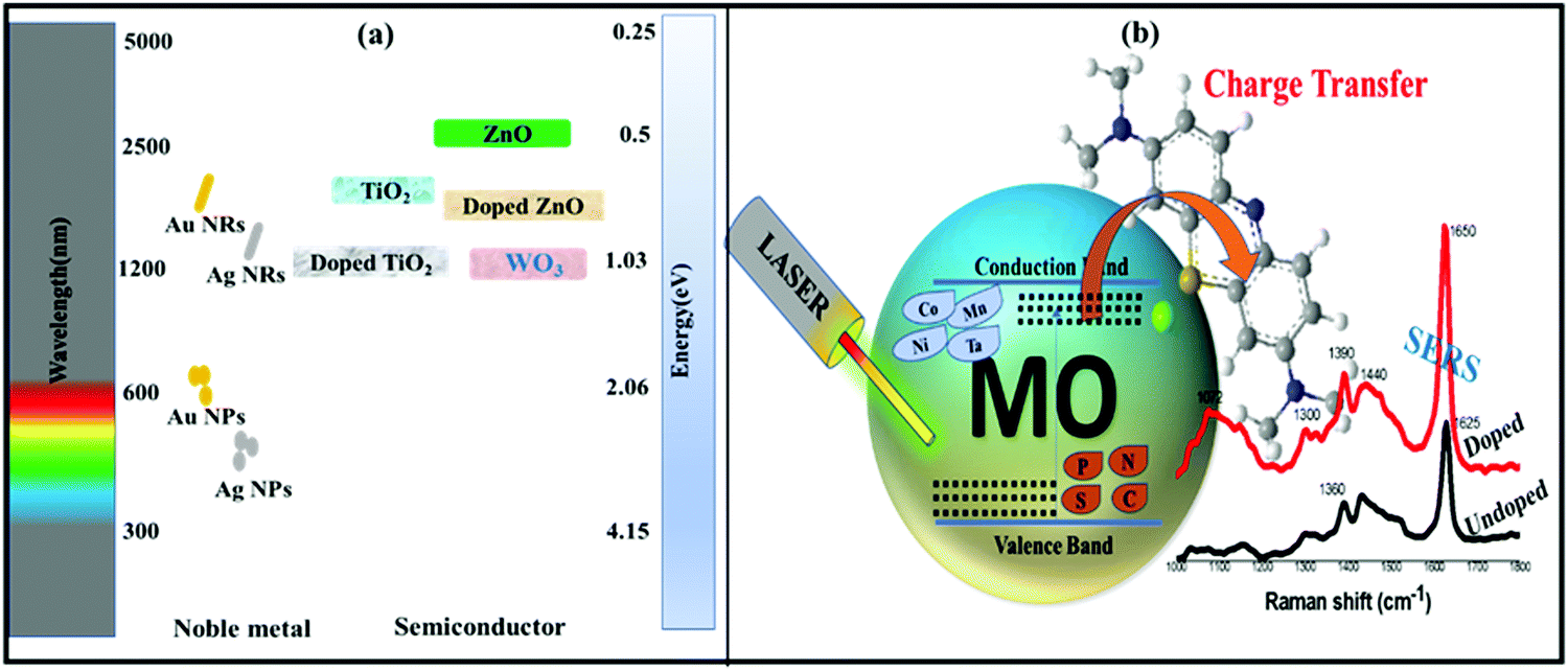 | ||
| Fig. 1 (a) Spectral regions of LSPR for different types of noble metal and metal oxide based semiconductor nanomaterials.37 (b) Schematic of tuning the band gap of semiconductor nanomaterials through metal and non-metal doping for enhanced SERS properties. | ||
In recent years, doping engineering has emerged as an excellent means for designing novel semiconductor nanostructures for SERS applications. Although doping engineering has been found to be beneficial for the development of semiconductor based SERS substrates with improved SERS sensitivity and recyclability, no systematic work has still been reported. This review deals with the doping engineering of metal oxide semiconductors for designing novel SERS substrates for ultrasensitive chemical and biochemical detection as well as recent developments in the field. Various doping strategies (i.e., metal and non-metal) to tune the properties of semiconductors (particularly metal oxide semiconductors) including improved optoelectronic properties and CT process for SERS applications with an emphasis on SERS enhancement mechanisms have been discussed in detail.
2. Fundamentals of CT and SERS mechanisms in metal oxide semiconductors
SERS is a surface phenomenon, where inelastic Raman scattering of an analyte molecule adsorbed on the surface of a SERS active substrate is enhanced under the influence of a laser beam.46–48 In the past years, development of semiconductor based SERS substrates, i.e. noble metal free SERS substrates, has gained considerable attention. The SERS investigation on metal oxide semiconductors exploits the applicability of Raman spectroscopy in producing excellent semiconductor based SERS substrates. As discussed in Section 1, among all noble metal free substrates, metal oxide semiconductors have received a lot of attention due to their promising properties such as physio-chemical stability, low toxicity, high refractive index, high reactivity, ease of synthesis, low cost, high catalytic activity, and high energy conversion efficiency. These properties enable their wide applications in various fields like photocatalysis, solar cells, transistors, light emitting devices, and sensing including SERS ultrasensitive detection.27,49 Copper chalcogenides are another emerging class of semiconductor nanomaterials showing a similar physical phenomenon to SERS substrates. Similar to metal oxides, these Cu chalcogenide nanomaterials show LSPR in the NIR region, attributed to the Cu vacancies.22,34–36 The high uniformity, tunable band gap, morphology dependent resonance and easy preparation of metal oxide semiconductors make them excellent SERS substrates.19 Semiconductor based SERS substrates promote direct CT between the adsorbed analyte molecule and substrate50 and have been engineered in many ways to show a SERS enhancement factor (EF) above 106 which is also very significant when compared to noble metal substrates.51 Noble metals, on the other hand, show better SERS EFs and also display a morphology-dependent LSPR and SERS enhancement. However, as discussed in Section 1, due to some limitations of noble metals in fabricating SERS substrates, research is also focused on semiconductor based SERS active materials which provide possible alternatives to noble metals.The mechanism behind SERS stems not from a single resonance process but involves Herzberg Teller vibronic coupling contribution of three resonances: SPR (Mie Resonance), CT resonance and molecular or excitonic resonance as depicted in Fig. 2(a). As reported in the literature, semiconductors with a low electron density show LSPR in the NIR region but not in the visible region as shown in Fig. 1(b).25,48,52,53 Yang et al.54 attributed the enhanced Raman signal to the coupled resonance as shown in Fig. 2(b). They observed that three resonances occurred simultaneously, that is, the wavelength of the laser is approximately similar to the molecular resonance wavelength (λlaser = λmol), Mie resonance wavelength (λlaser = λMie) and CT wavelength (λlaser = λCT) as shown in Fig. 2(b). It was demonstrated that when all the resonance processes take place simultaneously, then a significant enhancement is observed in the Raman signal.
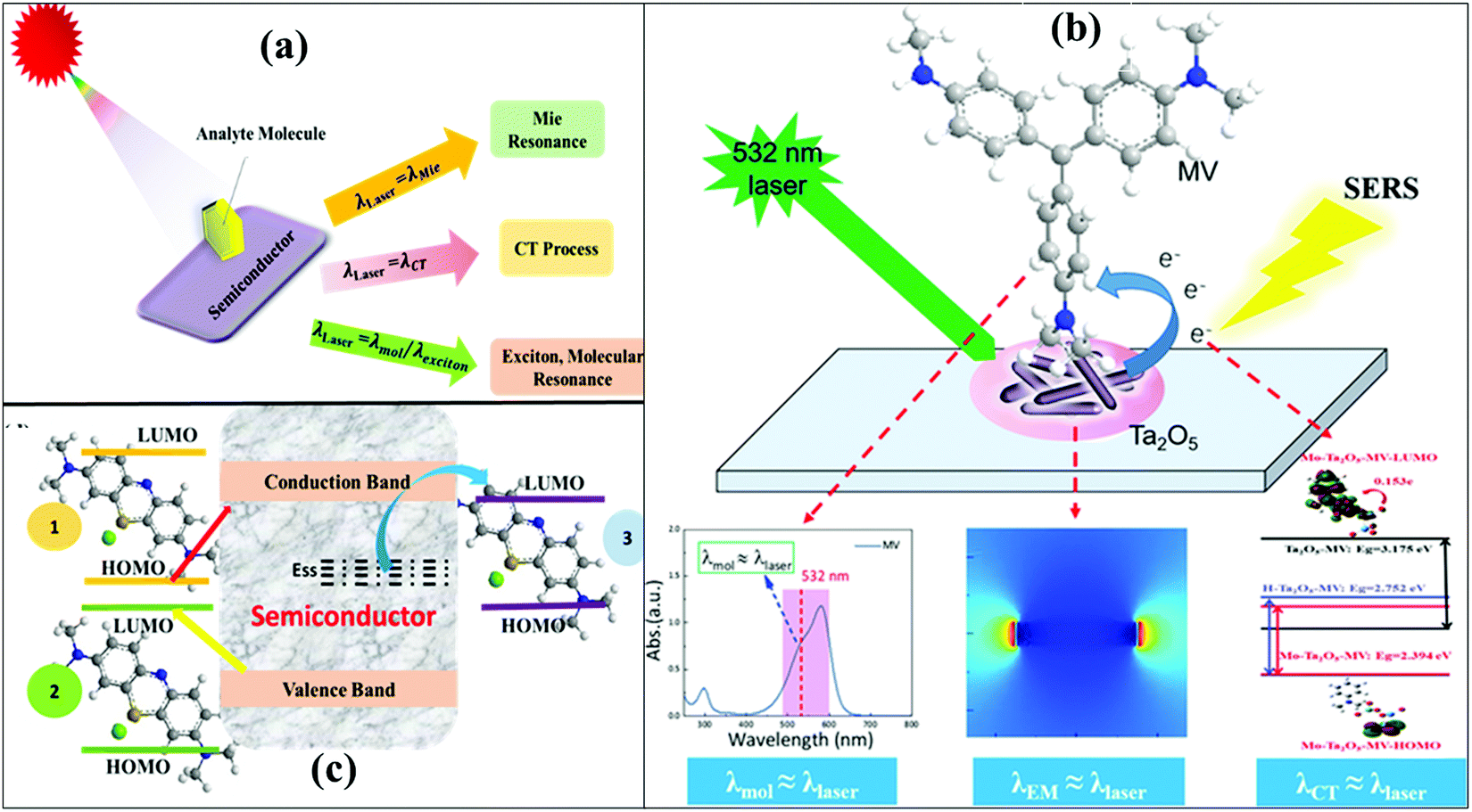 | ||
| Fig. 2 (a) Schematic showing the possible way to tune the SERS enhancement in semiconductor systems. (b) Diagram of the mechanism of the “coupled resonance” strategy on the semiconductor Ta2O5 SERS substrate.54 (c) The CT paths in semiconductor–molecule systems are (1) HOMO-to-CB, (2) VB-to-molecule LUMO, and (3) surface state-to-molecule LUMO. | ||
Mie resonance occurs in dielectric particles apart from noble metal nanoparticles (NPs), which enhances the local electromagnetic field near the dielectric material. It is a morphology dependent phenomenon, in which when the size of the NPs is almost equal to the wavelength of the incident light then an enhancement in the Raman signal is observed. According to Mie resonance in noble metal free substrates, the enhancement factor is proportional to the square of scattering efficiency.48 Ji et al.55 observed that the enhancement in the Raman signal of ZnO NPs originated from the mutual contribution of Mie resonance and the CT process. Also, Alessandri et al.56 reported that TiO2 shell-based nanostructures showed an enhanced Raman signal due to a high refractive index and multiple light scattering from the nanostructure. In molecular resonance, there is no need for a substrate, and there is a resonant Raman spectrum when the wavelength of the excitation laser beam is equal to the energy gap between the HOMO and LUMO of the molecule, then the Raman intensity is increased 3–4-fold.50,57
In the CT mechanism, the analyte molecule is chemically adsorbed on the substrate surface. This chemisorption leads to a change in the polarizability (α) of the analyte molecule attributed to the generation of new electronic states in the analyte molecule. As a result, the Raman spectra of chemisorbed species are modified in comparison to those of the corresponding free molecules.50 The main reason behind SERS enhancement in semiconductor substrates is the direct CT process occurring between the analyte molecule and substrate. The CT process could only be possible if the energy levels of analyte and substrates are in proper agreement with each other. So the choice of the analyte and substrate is also an important factor in the CT process. The CT process could be possible by different ways: (i) e− from the HOMO of the adsorbed molecule could be excited to the CB of the metal oxide semiconductor as shown in Fig. 2(c)–(1); (ii) e− from the valence band (VB) of the metal oxide semiconductor could be photoexcited to the LUMO of the adsorbed molecule as shown in Fig. 2(c)-(2); (iii) e− from the VB of the metal oxide could be excited to the sub-band gap energy levels of the metal oxide, followed by transfer to the LUMO of the adsorbed molecule as shown in Fig. 2(c)-(3).25,53 Apart from these three modes of CT, two other less known paths of CT also occur: e− transfer from the CT complex to the CB of the semiconductor (i.e. strong bonding between the molecule and substrate forms a CT complex) and e− transfer from the CB of the semiconductor to the HOMO of the adsorbed molecule.
Lombardi et al.58 provided an expression (eqn (1)) for the intensity of the lowest order non-zero contribution in which it is clear that these three resonance processes are not independent, but in fact are coupled by terms in the numerator. As given in the expression below, the denominator is the product of three different resonances (SPR, CT and molecular or excitonic) which shows that when all resonances occur the strongest enhancement is observed in the SERS signal.
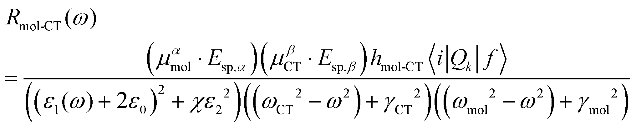 | (1) |
In the case of semiconductors, one more resonance occurs, i.e., excitonic resonance, because of their band gap. These are electron–hole pairs generated in solids by irradiation of light. To obtain the highest enhancement, the wavelength of the laser beam must lie within the range of one or more of these CT resonances. A new term ‘intensity borrowing’ also exists when the wavelength of the laser is slightly far apart from the resonance wavelengths. Then, it borrows intensity from excitonic or molecular resonances through Herzberg coupling. Mie resonance, when occurs in semiconductors, enhances the local electromagnetic field and is strongly dependent on the size of the NPs as well as on the wavelength of excitons. By knowing the excitonic wavelength (λex) and dielectric constant of the semiconductor substrate, the particle size at which plasmon resonance coincides with the excitonic wavelength can be calculated.53,59 For the optimization of the SERS EF, different pathways shown in Scheme 1 can be followed in order to obtain enhanced Raman signals.
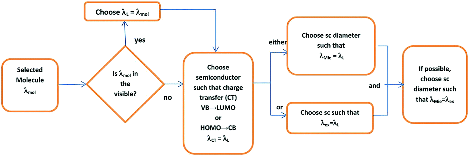 | ||
| Scheme 1 Flow chart of the optimization of the SERS EF of an analyte molecule.60 | ||
Firstly, if molecular resonance occurs in the visible region, then the laser beam should have the wavelength in this region, i.e., λL = λmol, and also the excitonic or plasmon resonance must be near λmol to obtain the enhanced SERS signal. Secondly, if the molecular resonance falls in the UV region, then the selection of semiconductor should be carried out in such a way that CT from the VB or CB edge to the molecule must be close to the laser beam wavelength, i.e., L = λCT. Another way is that the excitonic wavelength of the semiconductor is nearly equal to the CT, i.e., λex =λCT. This most commonly happens when the band gap of the semiconductor lies in the visible region. However, in some cases when the particle size is equal to the Bohr radius (1–10 nm), then the excitonic transition shifted to higher energy values. Therefore, the tuning of the particle size is an important parameter to get the excitonic wavelength equal to CT. If the particle size is around 100–300 nm, then Mie resonance occurs by controlling the various parameters such as particle size, morphology, optimized doping, etc. When Mie resonance and excitonic resonance coincide, then there is a large enhancement in the SERS signal.60
The metal oxide semiconductor nanomaterials serve as an excellent SERS substrate mainly through the CT mechanism as discussed above and shown schematically in Fig. 2(c). Metal oxide semiconductor nanomaterials are important for SERS applications because they are easy to prepare and modify in view of their tunable optical properties.26,54,61–63 As discussed above, most of the Raman spectrophotometers use lasers with wavelengths higher than 500 nm (or energy <2.5 eV) to study the SERS enhancement. Due to the wide band gap of metal oxide semiconductors, i.e. >3.0–4 eV (exciton resonance), and also the larger energy gap between the HOMO and LUMO of the molecules, i.e., >3.0–5.0 eV (molecular resonance), as compared to the excitation energy provided by the laser, these CT resonances are not possible in such systems. The excitation energies provided by the lasers are not sufficient to excite the electrons from the VB to the CB of metal oxide semiconductors or from the HOMO to the LUMO level of the adsorbed molecules. However, it has been found that there are plenty of surface defects (i.e., surface oxygen vacancy defects), which can bind these excited electrons and form the so-called surface state energy levels (Ess) below the CB in metal oxide semiconductors. Further, it is possible to excite the electrons from the VB to the low-lying surface states using these exciting laser sources as shown in Fig. 2(c). For example, Yang et al.53 reported that the intrinsic semiconductor surface states (surface defect) play an important role in the metal oxide-to-molecule CT process, both as electron traps and as intermediate states for electron transfer to molecules. The plentiful surface states were found to be favorable to a metal oxide-to-molecule CT process. In TiO2, these surface states are located at a position 0.5 eV lower than the CB edge.64 The pathway of CT also depends on the band alignment between the semiconductor and target molecule. In order to show an optimum CT between the semiconductor and target molecule, it is necessary that the energy level of semiconductors should be well matched with that of the target molecule. Yang et al.65 studied the SERS enhancement of levofloxacin (LVFS) drug molecules on TiO2 and explained it on the basis of the CT mechanism through surface states. The laser with a wavelength of 532 nm (2.33 eV) was used which was not enough to enable the transition of electrons from the VB to CB of TiO2 NPs (the bandgap is 3.2 eV) or from the HOMO level to the LUMO level (the HOMO–LUMO gap is 3.92 eV) of LVFX molecules. Due to the Ess level (0.5 eV lower than the TiO2 CB) present at little higher than the LUMO level of the LVFS molecule, the energy of the laser used (532 nm) was found suitable to excite the electrons from the VB levels to the Ess levels of TiO2, and then the electrons move to the LUMO level of LVFX molecules following the TiO2-to-molecule CT process through Ess.
In spite of many important aspects of metal oxide semiconductor nanomaterials mentioned above, there are some limitations that hinder their proper and straightforward applications. These limitations include their wide band gap (i.e., 3.0–4.0 eV), LSPR observed in the NIR region, and high charge carrier recombination rate. Due to the large band gap, most of the metal oxide semiconductors absorb UV light and also show a high recombination rate of charge carriers leading to low CT and lower SERS enhancement as well as photocatalytic activity. These characteristics do not allow simply the CT process and therefore restrict their use as potential SERS substrates. To overcome these drawbacks, metal oxide semiconductor nanomaterials are modified by a variety of ways such as surface modification, doping, formation of hybrid nanostructures with other functional nanomaterials, etc. Doping engineering of metal oxide semiconductor nanomaterials is one of the promising methods. It provides an easy way to engineer their band gap, morphologies and hence the optoelectronic properties, which facilitate the CT process which is very important for SERS activity. In the next section, doping engineering of metal oxide semiconductors has been discussed using metal and non-metal elements emphasizing their role in improving the CT SERS enhancement.
3. Doping engineering of metal oxide semiconductors for enhanced CT and SERS activities
Doping engineering of metal oxide semiconductor nanomaterials is the most suitable method to tune their energy band gap and promote CT between the target molecule and semiconductor substrate. In recent years, substantial research has been carried out on doping engineering in metal oxide semiconductors to improve their optical, electrical, structural, surface and interface properties for several applications including photocatalytic degradation and SERS sensing. It has been realized that, by introducing foreign elements via doping engineering, the transformation of non-SERS metal oxide semiconductors to active SERS substrates can be done successfully. Thus, doping engineering has become an important strategy for adjusting plasmon-free SERS performance.48 Doping generates defects which help in increasing the charge carrier density by transferring electrons or holes as shown in Fig. 3(a).27,66 It does not only introduce defects into semiconductors but also changes the lattice constant, bond energy, and energy gap of semiconductors. An appropriate choice of doping elements and tailoring of morphology can promote charge separation efficiency and consequently increase the number of electrons reaching the surface of the substrate, which can tune the CT process. Besides, it has also been shown that the content of surface defects and the surface area of metal oxide semiconductors increase with increasing dopant concentration, which also promotes the semiconductor-to-molecule CT process. Therefore, doping engineering in metal oxide semiconductors provides an additional semiconductor-to-molecule CT besides the intrinsic semiconductor-to-molecule CT process, which is responsible for a higher SERS enhancement in such semiconductor–molecule systems.67 Doping engineering is the most effective and easy way to tune the surface as well as optoelectronic properties of metal oxide semiconductor nanomaterials for improving SERS performance with reproducibility and recyclability which has been discussed below in detail.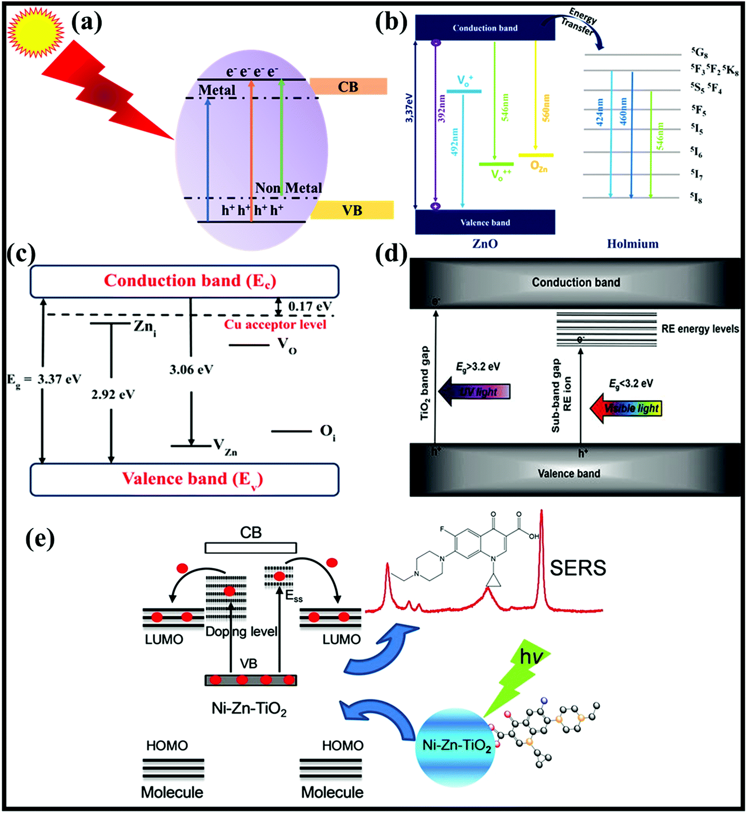 | ||
| Fig. 3 (a) The doped levels formed by metal and non-metal doping in a metal oxide semiconductor. (b) Ho3+ free-ion doped energy level diagram and ZnO energy level diagram. Reprinted with permission from [Springer Nature] [J. Mater. Sci.: Mater. Electron.] [ref. 71 Holmium (Ho)-coated ZnO nanorods: an investigation of optoelectronic properties, M. Achehboune, M. Khenfouch, I. Boukhoubza, B. M. Mothudi, I. Zorkani and A. Jorio] [Copyright] (2020). (c) Cu doped ZnO energy level diagram. Reprinted from ref. 68, A. SreedharJin H. Kwon, J. Yi, J. S. Kim and J. S. Gwag, Enhanced photoluminescence properties of Cu-doped ZnO thin films deposited by simultaneous RF and DC magnetron sputtering, Mater. Sci. Semicond. Process., 49, 8–14, Copyright (2016) with permission from Elsevier. (d) Band gap engineering in TiO2 with RE doping.70 (e) The charge transfer between the adsorbed molecule and Ni–Zn–TiO2 contributed to SERS. Copyright (2017) John Wiley and Sons. Used with permission from (X. Jiang, K. Song, X. Li, M. Yang, X. Han, L. Yang and B. S. Zhao, Double Metal Co-Doping of TiO2 Nanoparticles for Improvement of their SERS Activity and Ultrasensitive Detection of Enrofloxacin: Regulation Strategy of Energy Levels, ChemistrySelect).73 | ||
Doping with metals or non-metals creates sub-energy (surface defects) levels between the CB and VB of semiconductors as shown in Fig. 3(a–e). These defect levels trap the photogenerated electrons and reduce the band gap and further enhance the CT process between the substrate and target molecules inhibiting the charge carrier recombination. Reduction in band gap depends upon the concentration of the dopant and also the type of doping. Mainly two types of doping are generally observed in metal oxide semiconductors: substitutional and interstitial doping which depend on the kind of dopant. When the size of the dopant is comparable to the one of the component of the metal oxide semiconductor, then substitutional doping takes place, otherwise interstitial one occurs.27 Generally, metal and non-metal dopants have been used for engineering metal oxide semiconductor nanomaterials for SERS applications. Interestingly, significant SERS enhancement has been observed. Here, metal and non-metal doping in metal oxide semiconductors are discussed in view of their significant role in producing plasmon free excellent SERS substrates.
3.1 Metal doping
Metal doping has extensively been used to tune the structural, optical and electrical properties of metal oxide semiconductors for sensing, photocatalysis, solar cell, SERS and many other applications. In the last few years, extensive research has been carried out with an emphasis on improving the surface and interface properties of metal oxide semiconductors by doping using various metals (i.e., transition and rare earth metals) in order to improve their CT properties for studying the SERS activity. In the case of transition metals, generally substitutional doping occurs due to the similar size of transition metal dopant ions to that of the metal ions of semiconductors. Mainly transition metals from the group representing the 3d, 4d, and 5d series have been used as dopants. The transition metals in the 3d series usually have a size comparable to that of metal ions in metal oxides. For example, Cu2+ has an almost comparable size to Zn2+ ions so it can easily substitute Zn on doping into the ZnO lattice. Due to doping, there is formation of acceptor levels below the CB which enhance the CT process in Cu doped ZnO NPs. As shown in Fig. 3(c) the ZnO lattice has other defect states such as zinc vacancies (VZn), oxygen vacancies (VO), interstitial zinc (Zni) and interstitial oxygen (Oi). Among these, VZn and Oi behave as acceptor defects and Zni and VO act as donor defects.68 For 4d, 5d series metals, higher oxidation states are possible which make their sizes comparable to those of the metal ions of semiconductors due to a higher nuclear charge. For example, Ta doped TiO2 nanofibers (TNF)26 exhibited substitution doping because of the similar size of Ta5+ (dopant ion) and Ti4+ ions (TiO2) which led to Ti3+ defect conditions being generated below the CB of TiO2. These Ti3+ defects captured the photogenerated electrons, thereby enhancing the CT process as well as the SERS signal of methylene blue (MB) molecules. Similar results were observed by Jing et al.69 for self-doping of Ti3+ in TiO2 and Xue et al.61 for Mn doping in TiO2 NPs.Rare earth metal ions have larger sizes as compared to the metal ions in metal oxide semiconductors. Therefore, doping with rare earth metals is a slightly complicated process as compared to transition metal doping. The doping process is generally carried out by using rare earth metals with a higher oxidation state so that their size can be compared to the metal ions of the metal oxide semiconductor and they can replace the metal ions. The main principle involved in such processes is again the formation of acceptor levels below the CB which act as trapping centers for photoexcited electrons as shown in Fig. 3(d).70 These trapping centers created by rare earth metal ions trap the electrons similar to that of doping involved in transition metals. These trapping centers are created by empty 4f orbitals which take up electrons in these orbitals. This trapping prevents the electrons from recombining, thereby increasing the activity of metal oxide semiconductors.27 For example, as shown in Fig. 3(b) Ho3+ doping in the ZnO lattice creates a charge imbalance and creates trapping centers formed by 4f orbitals, and these defect levels trap the charge carriers and thus enhance the properties of ZnO NPs.71 Similarly, Li et al.54 synthesized Ga doped ZnO NPs and observed that Ga doping generated new levels below the CB and reduced the band gap of the ZnO crystal. Doping of Ga narrowed the band gap up to a minimum value of 3.16 eV which further promoted the CT resonance process from the VB of ZnO NPs to the LUMO of 4-MBA molecules.
In most of the cases, it has been reported that rare earth metals form an oxide layer on the surface of metal oxide semiconductor nanomaterials and substitutional doping is not observed. The oxide layers formed by rare earth metals have defects which again trap the photoexcited electrons produced from the VB of the semiconductors under the effect of electromagnetic radiation. The oxide layer prevents the electron–hole pair from recombining and enhance CT as well as SERS activities.27,72 For example, Gao et al.62 studied Nd doping in ZnO nanocrystals and described that a higher Nd concentration led to the formation of an oxide layer acting as a trap center and prevented e−/h+ pair recombination. Doping could generate new doped energy levels or Nd3+ defect levels below the CB of ZnO which facilitated CT between ZnO and 4-MPy and mainly it was found responsible for the enhanced SERS activity.
3.2 Non-metal doping
In non-metal doping, heteroatoms with a size comparable to that of oxygen (O) in metal oxide semiconductors generally show substitutional doping and replace O ions, creating imperfections within the crystal structure. Valentine et al.74 performed periodic DFT calculations to study the doping effect of non-metals in anatase TiO2. It was demonstrated theoretically that doping with non-metals creates localized states in the lattice which facilitate visible light absorption. In non-metal series such as B, C, N, O and F, effective nuclear charge plays an important role in the position of the dopant 2p states as shown in Fig. 4(a). The main cause of the formation of these donor levels is due to the overlapping of 2p–2p and 2p–3p orbitals depending upon the non-metal used as the dopant. Due to this overlapping, the gap between the VB and CB decreases, thereby facilitating the easy flow of electrons from the lower to the upper level. For example, Zhang et al.17 described that N doping in bicrystalline TiO2 nanocrystals created donor levels above the VB which reduced the band gap and enhanced the optical and CT properties useful for SERS enhancement.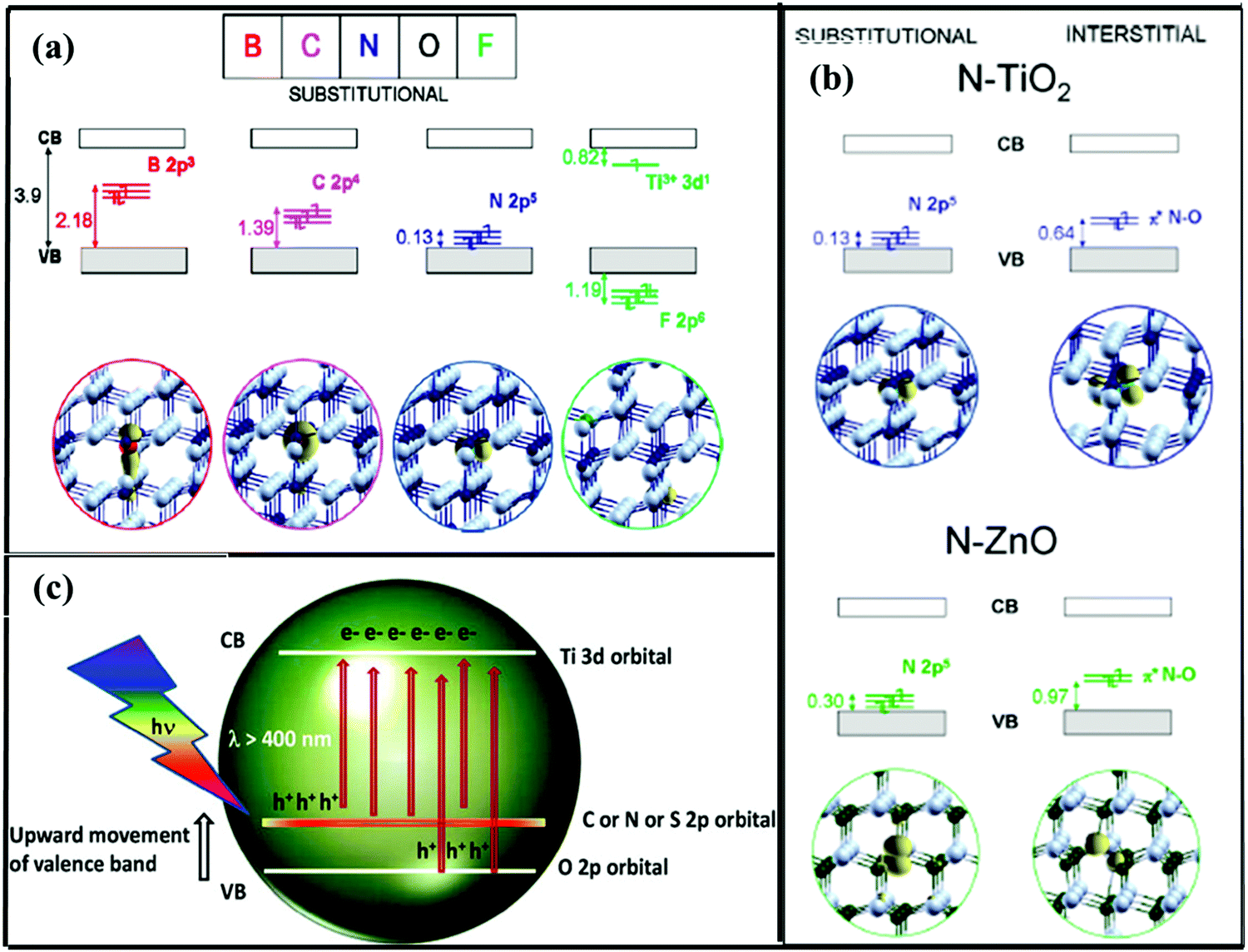 | ||
| Fig. 4 (a) Substitutional doping of non-metals in the TiO2 lattice. Reprinted from ref. 74, C. Di Valentin and G. Pacchioni, Trends in non-metal doping of anatase TiO2: B, C, N and F, Catal. Today, 206, 12–18, Copyright (2013), with permission from Elsevier. (b) Schematic representation of the band gap of the material (top) and ball-and-stick representation (bottom) of substitutional (left) and interstitial (right) N impurities in anatase TiO2 and wurtzite ZnO. Ti atoms are in blue, Zn atoms in green, O atoms in gray, and N atoms in light blue. Reprinted (adapted) with permission from ref. 75 {C. Di Valentin and G. Pacchioni, Acc. Chem. Res., 2014, 47, 3233–3241}. Copyright {2014} American Chemical Society. (c) Upward movement of the valence band in the C or N doped TiO2 lattice. Reprinted from ref. 76, P. A. K. Reddy, P. V. L. Reddy, E. Kwon, K.-H. Kim, T. Akter and S. Kalagara, Recent advances in photocatalytic treatment of pollutants in aqueous media, Environ. Int., 91, 94–103, Copyright (2016), with permission from Elsevier. | ||
As discussed above, doping engineering in metal oxide semiconductor nanomaterials provides an additional semiconductor-to-molecule CT besides the intrinsic semiconductor-to-molecule CT process responsible for higher SERS enhancement.65 It occurs due to the production of much more defects and reduced band gap or shrinkage of band gaps between the VB and CB of metal oxide semiconductors (Fig. 3e). However, other CT processes as discussed in the last section and shown in Fig. 2, which do not involve the electron transitions through surface states, are still forbidden due to the large energy gap. Due to doping induced additional surface defects and band gap shrinkage, the CT process through the additional surface state is influenced. It has been shown that doping of metals or non-metals along with the kind of doping (interstitial or substitutional) can shift the surface state levels in metal oxide semiconductors as shown in Fig. 3(a). Valentin et al.75 have theoretically shown that mainly two types of doping occur in TiO2 and ZnO lattices depending upon reaction conditions. As shown in Fig. 4(b), Ns and Ni represent the substitutional and interstitial doping of N atoms in TiO2 and ZnO lattices, respectively. The donor levels of Ns lie near the VB as compared to Ni, attributed to the rearrangement taking place during these two processes. When substitutional doping takes place, an O atom (grey) is substituted by the N (light blue) dopant. The substitutional doping does not require a very complex rearrangement and its energy states lie only 0.13 and 0.30 eV above the VBs of TiO2 and ZnO, respectively. However, in the case of interstitial doping, there are chances that the N dopant may be inserted in a lattice of two adjacent Zn/Ti ions. This forms a complex rearrangement which shifts the energy states to higher values such as 0.64 and 0.97 eV in TiO2 and ZnO, respectively, as shown in Fig. 4(b).
Doping engineering with non-metals such as C, N and S facilitates the upward movement of the VB as shown in Fig. 4(c).76 As mentioned above, the type of dopant and nature of doping (i.e. substitutional or interstitial doping) influence the optical and CT properties of metal oxide semiconductors for SERS applications. It can affect the internal structure of the host lattice and cause distortions with generation of new bonds which further affect its properties. Doping is one of the most promising methods to form SERS active substrates and is also economically favorable, and has shown a significant impact in improving their SERS performance as plasmon free SERS substrates as discussed in the next section.
4. SERS performance of metal oxide semiconductor nanomaterials through doping engineering
In the past few years, the strategy of band gap engineering of metal oxide semiconductors through metal or non-metal doping has been followed to tailor and improve the structural, optical, electronic, morphological and surface properties for excellent SERS performance. Additionally, doping engineering provides unique strategies to control various factors to understand the metal oxide semiconductor to molecule CT process that contributes to SERS enhancement.77 This section provides details on the improvement of such properties of metal oxide semiconductors induced by metal or non-metal doping with an emphasis on improving their SERS performance as plasmon free SERS substrates.4.1 Doped TiO2 nanostructures for SERS applications
TiO2 is the most favorable semiconductor nanomaterial known to date due to its physical and chemical stability, low toxicity, high energy conversion efficiency, etc. TiO2 nanostructures show unique optical, structural, electrical, and photocatalytic properties, etc. and are therefore widely used in several fields such as in waste water treatment, antibacterial activity, solar cells, fuel cells, sensors, coating (as a self-cleaning material), etc.38,49,78Yang et al.64 reported that TiO2 showed an enhancement in the Raman signal of the adsorbed 4-MBA molecule due to the CT process between 4-MBA and the TiO2 substrate which further depended upon the surface properties and internal defects of TiO2. Various other parameters such as size, shape, phase, pH, etc. also affect the SERS activity of TiO2. The size of TiO2 nanostructures has been shown to have a direct relationship with the increase in the intensity of Raman signals. Xue et al.79 observed a variation in the intensity of Raman signals when the crystallite size of TiO2 increased from 6.8 to 14.2 nm and a maximum enhancement was observed at a 10.2 nm crystallite size. It was also reported that the phases of TiO2 also impact the SERS activity. Yang et al.80 described that the mixed phase of TiO2 (85% anatase and 15% rutile) showed a SERS signal comparable to the anatase phase. The mixed phases not only reduced the recombination rate of charge carriers but also improved the CT process by enriching the surface defects, thus enhancing the SERS signals. Similarly, the pH of the solution also plays an important role in SERS enhancement. For example, Yang et al.81 studied the SERS activity of TiO2 by changing the pH of the solution and observed that it led to a change in the chemical adsorption of molecules on the surface sites present on TiO2 affecting the CT process that further improved the SERS activity. Similarly, the shape of nanostructures is also responsible for optimizing the SERS activity, for example, 1D nanostructures are known for the unidirectional flow of photogenerated electrons which reduces the recombination rate of charge carriers contributing to the CT process and enhances the SERS signals.26
However, it has been realized that bare TiO2 needs to be modified in order to improve its optical, electronic and surface properties for better SERS performance due to its wide band gap and less availability of surface states. It leads to insignificant CT properties and an enhancement in SERS signals. Doping engineering of TiO2 nanostructures and analysis of their SERS activity have gained much attention in the past years using various metals or non-metals (i.e., Mn, Co, Ti, Fe, Mg, Ta, Ni, N and C), which led to an improvement in their optoelectronic and surface properties in view of enhanced SERS activities. Dopant concentration is one of the important parameters that plays a significant role in the enhancement of various properties including enhanced visible light activity for photocatalysis and SERS applications.17,77,82 Xue et al.61 studied the effect of Mn doping on SERS activity in TiO2 NPs for the detection of 4-MBA molecules. It was observed that an increase in the Mn concentration redshifted the absorption spectra of doped TiO2 NPs, indicating an increased defect concentration. It was found that 3% Mn doped TiO2 NPs exhibited a maximum SERS intensity by a factor of six as compared to the native enhancement of 4-MBA adsorbed on undoped TiO2 NPs attributed to the doping induced improved CT mechanism as shown in Fig. 5(a–c). As discussed in Section 3, Raman signals are enhanced by the incorporation of doped metal ions which enrich the surface states and improve the photo-generated carrier separation efficiency, leading to an enhancement in the TiO2-to-molecule CT process. Similar results were observed in the case of Co-doped TiO2 NPs for SERS enhancement of 4-MBA molecules.83 A detailed study revealed that Co2+ ions were incorporated into the TiO2 lattice and defects were created due to the substitution of Co2+ ions for the Ti4+ ions which were found beneficial for CT so as to improve the SERS activities. In addition, it has been demonstrated that doping can induce surface defects, lattice defects or abundant doped energy levels below the CB which facilitate the photogenerated charge separation and promote the CT mechanism.77 Singh et al.26 studied the dual functional behavior of Ta doped TiO2 nanofibers as shown in Fig. 5(d). 5% Ta doped TiO2 NFs exhibited the highest SERS signals of adsorbed MB molecules (Fig. 5e). The incorporation of Ta5+ ions into the TiO2 lattice led to the generation of a surface energy level below the CB which helped in CT and improved the SERS and photocatalytic activities (Fig. 5f).
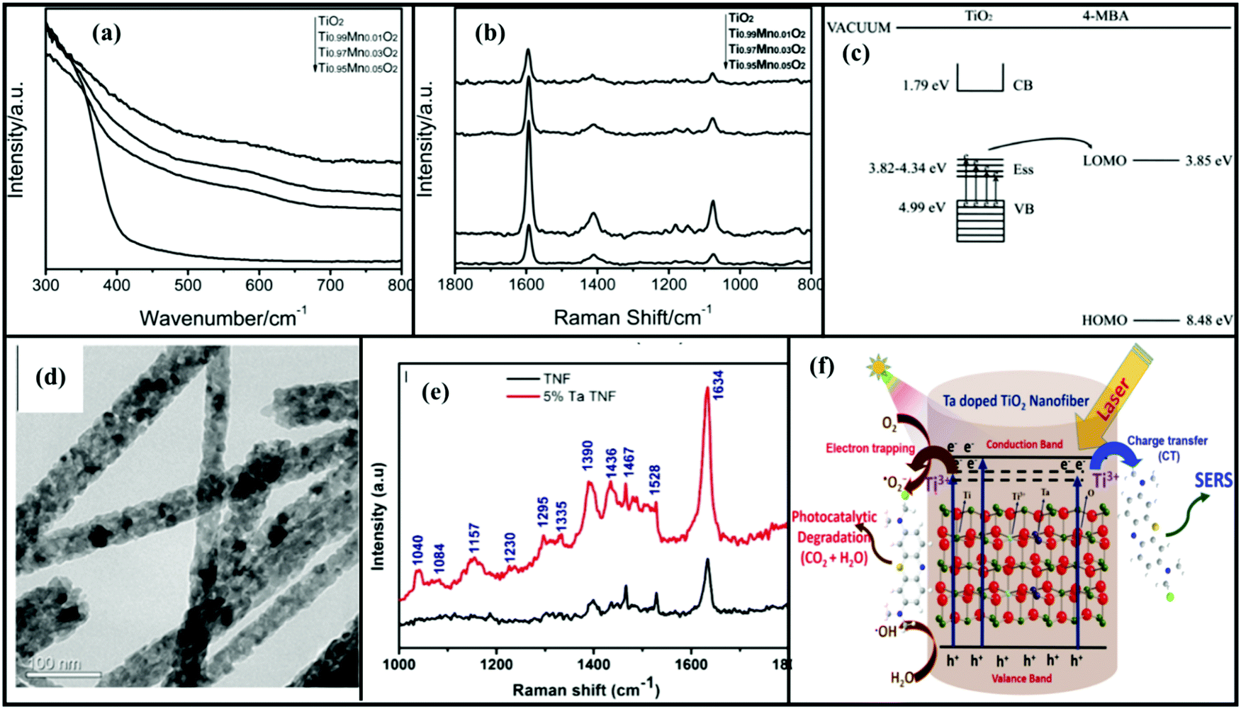 | ||
| Fig. 5 (a and b) UV absorption spectra and SERS spectra of 4-MBA molecules adsorbed on TiO2 (using a laser with a wavelength of 514.5 nm) and Mn–TiO2 NPs. (c) Schematic of the CT mechanism for SERS of 4-MBA adsorbed Mn–TiO2 nanoparticles. Reprinted from ref. 61, X. Xue, W. Ji, Z. Mao, Z. Li, W. Ruan, B. Zhao and J. R. Lombardi, effects of Mn doping on surface enhanced Raman scattering properties of TiO2 nanoparticles, Spectrochim. Acta, Part A, 95, 213–217, Copyright (2012), with permission from Elsevier. (d) SERS spectra of TiO2 and Ta doped nanofibers. (e) TEM image of Ta doped TNF. (f) Schematic of the mechanism of enhanced photocatalytic degradation and SERS performance (using a laser with a wavelength of 532 nm) of Ta-doped TiO2 nanofibers (TNF-TiO2 nanofibers). Reprinted with permission from ref. 26 {N. Singh, J. Prakash, M. Misra, A. Sharma and R. K. Gupta, ACS Appl. Mater. Interfaces 2017, 9, 28495–28507}. Copyright {2017} American Chemical Society. | ||
Similarly, Xue et al.84 reported similar SERS performance of Mg doped TiO2 NPs by studying the enhancement of vibrational and phonon modes of Mg doped TiO2 NPs using 4-MBA molecules. It was observed that the optimum dopant concentration (3% Mg) improved the visible light absorption by enriching surface defects which further enhanced the CT, resulting in enhanced SERS performance (Fig. 6a–c). The absorption edge extension towards longer wavelengths indicates that there is a good contact between TiO2 and Mg2+ ions.84
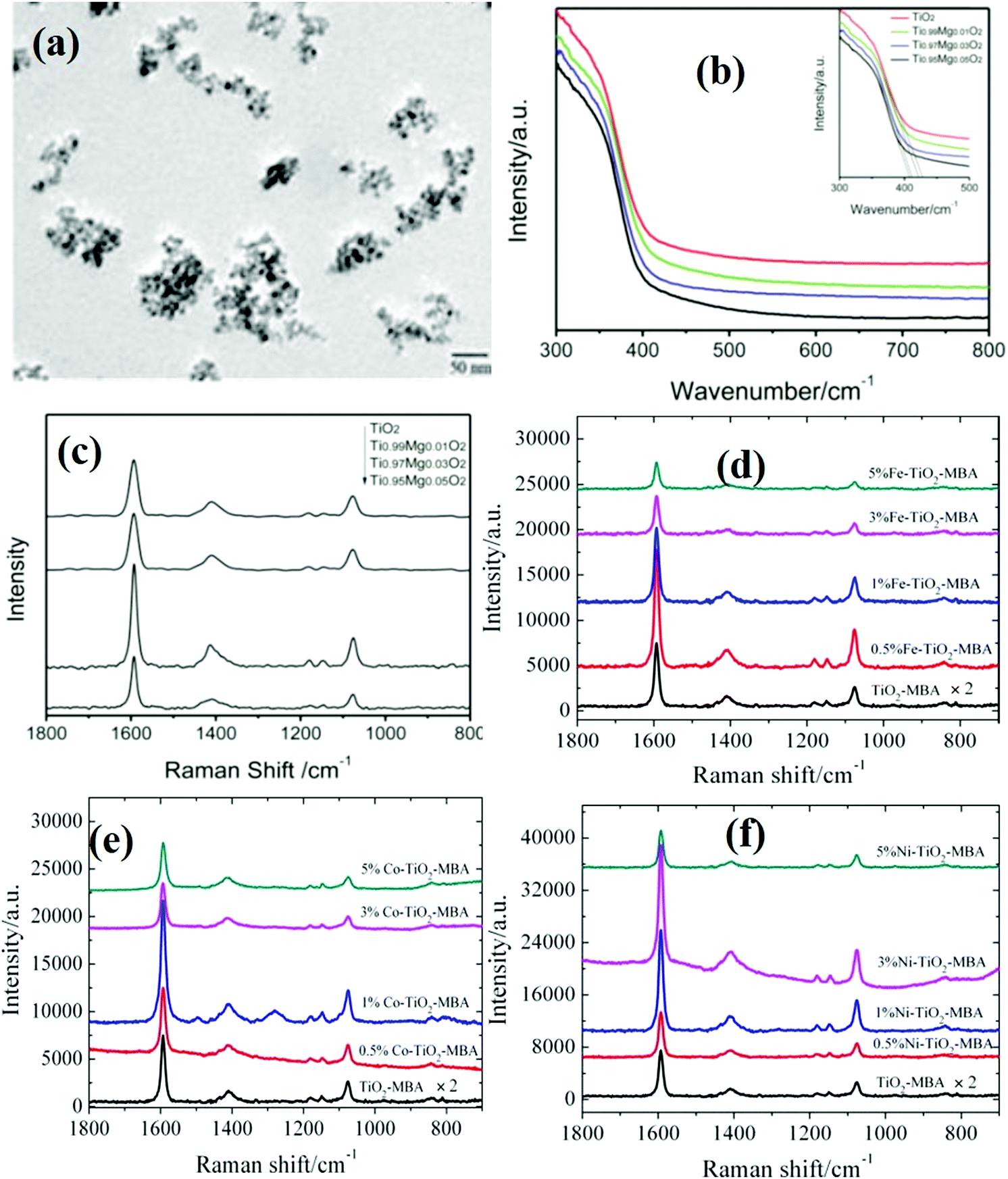 | ||
| Fig. 6 (a) SEM image of Mg doped TiO2 NPs. (b and c) UV and SERS spectra (using a laser with a wavelength of 514.5 nm) of pristine TiO2 and Mg (1, 3 and 5%) doped TiO2.84 (d–f) SERS spectra of Fe, Co and Ni doped TiO2 NPs, respectively, using a laser with a wavelength of 514.5 nm. Reprinted from ref. 77 [L. Yang, X. Jiang and M. Yang, Appl. Phys. Lett. 2011, 99, 111114], with permission from AIP Publishing. | ||
It has also been emphasized that the electronegativity of doped ions can affect the electron cloud densities on the constituent ions (Ti and O ions in the case of TiO2) of the metal oxide semiconductors within the lattice and can modify the band structure as well as CT properties.77 In addition, the ionic radius of dopants can also lead to differences in optimal doping concentration for doping of different species into the TiO2 crystal lattice.77 For example, Yang et al.77 studied metal doping strategies in TiO2 NPs using different metal ions (Fe3+, Co2+, and Ni2+) and their effect on SERS performance. A wide optical absorption was observed below 410 nm for undoped TiO2 attributed to the VB to CB transition, whereas a broad absorption in the visible region of 410–760 nm was observed in the case of doped TiO2 NPs attributed to the transition from the VB to various doped energy surface levels generated by metal ion doping within the band gap. It was found that the amount and intrinsic nature of doping ions both showed a significant impact on band gap engineering. It further enhanced the CT process for a better SERS activity of TiO2 NPs doped with various metal ions. It was concluded that the SERS properties of such metal oxide semiconductors can be tailored by tuning the doping amount and doping species. The optimum doping amounts for different metals ions, namely, Fe3+, Co2+, and Ni2+, were found to be 0.5%, 1%, and 3%, respectively, for the maximum SERS enhancement in each case as shown in Fig. 6(d–f). The surface defects generated by doped metal ions are generally useful in CT and considered to be responsible for SERS enhancement. However, it was demonstrated that doping energy levels contributed more to the enhancement of the SERS activity as compared to the surface defects.
Interestingly, co-doping of TiO2 nanostructures with metal ions significantly enhances the SERS activity. Jiang et al.73 performed a comparative study of SERS activities on undoped TiO2 and Zn/Ni metal doped/co-doped TiO2 NPs, i.e. Zn–TiO2, Ni–TiO2 and Ni–Zn–TiO2. It was observed that co-doped (Ni–Zn–TiO2) NPs exhibited a better SERS response as compared to mono- and undoped TiO2 NPs as shown in Fig. 7(a–c). Metal co-doping provides more defect induced surface states as well as doped energy levels below the CB, which improved the CT process for SERS enhancement. The UV absorption spectra (Fig. 7b) showed visible light absorption with an absorption peak tailing around 410–490 nm which was attributed to the presence of surface states. Another broad absorption peak around 650 nm was attributed to the doped energy levels in co-doped TiO2 NPs. These abundant surface and doped levels facilitated the CT process as schematically demonstrated in Fig. 3(e). The enhanced SERS activity was studied to detect the enrofloxacin drug with a lower detection limit of 3 × 10⁻¹⁰ M. Jing et al.69 studied a novel way to synthesize Ti3+ self-doped TiO2 nanofilms by adjusting the oxygen flow during preparation to control the amount of Ti3+ dopant. It was reported that films with minimum oxygen flow contained the highest Ti3+ content and the lowest band gap among all the prepared TiO2 films, indicating that most oxygen deficiencies were present in it. SERS studies revealed that TiO2 films with a higher concentration of Ti3+ dopant and oxygen vacancies helped in the CT process and exhibited a maximum enhancement as shown in Fig. 7(d and e). The oxygen vacancies led to the generation of energy levels above the VB, helped in the excitation of electrons and increased the interfacial CT process which further enhanced the SERS signals.
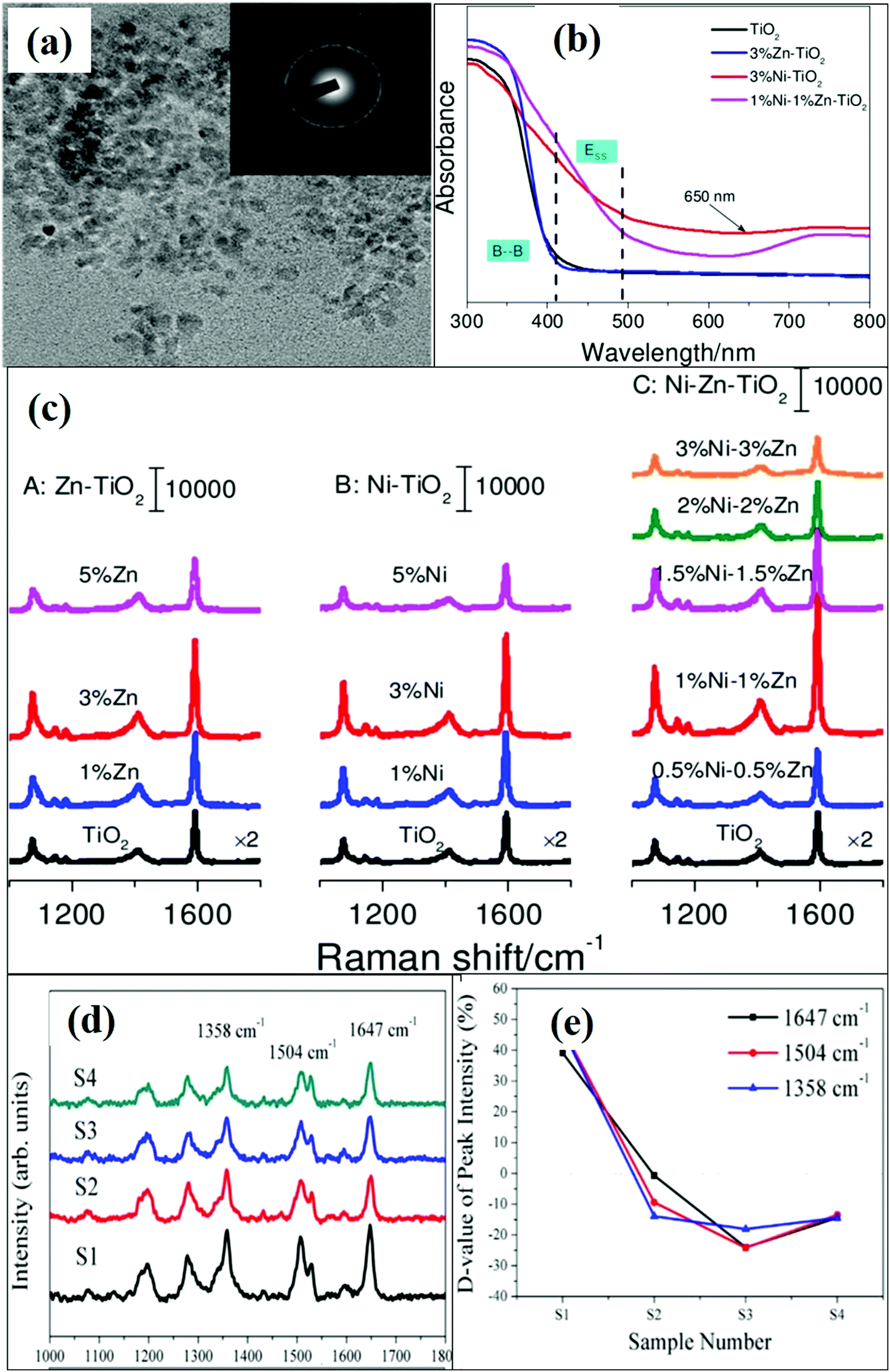 | ||
| Fig. 7 (a) TEM images and SAED pattern of 1%Ni–1%Zn–TiO2. (b and c) UV and SERS spectra of undoped and co-doped TiO2 NPs. Copyright (2017) John Wiley and Sons. Used with permission from (X. Jiang, K. Song, X. Li, M. Yang, X. Han, L. Yang and B. S. Zhao, Double Metal Co-Doping of TiO2 Nanoparticles for Improvement of their SERS Activity and Ultrasensitive Detection of Enrofloxacin: Regulation Strategy of Energy Levels, ChemistrySelect).73 (d and e) Raman spectra of the analyte molecule deposited on Ti self-doped TiO2 NPs under different oxygen flow rates. Reprinted from ref. 85, M. Jing, R. Hong, W. Wei, C. Tao, D. Zhang and S. Zhuang, Difference of SERS ability from titanium oxide films by Ti3+ self-doping, Opt. Mater., 73, 371–376, Copyright (2017), with permission from Elsevier. | ||
The crystalline nature of a metal oxide semiconductor based SERS substrate also affects CT properties. Zhang et al.17 synthesized bicrystalline TiO2 NF based SERS substrates which enabled additional CT across the interface and thus showed enhanced CT activity in comparison to the single crystalline phase. N doping in bicrystalline TiO2 NFs was performed by varying the calcination temperature (500, 600 and 700 °C). Slit shaped nanopores were observed at 600 °C and an increase in temperature collapsed the pores as shown in Fig. 8(a and b) which restricted further N doping. The absorption spectra showed a red shift with doping till 600 °C, whereas a decrease in absorption was observed at 700 °C. The XPS spectra also confirmed that the sample calcined at 600 °C had a higher content of N due to its porous structure. SERS activity was studied through adsorption of 4-MBA molecules on bicrystalline TiO2 NFs. From the SERS spectra shown in Fig. 8(b), it can be seen that N doped TiO2 NFs calcined at 600 °C showed the most enhanced SERS signals. N doping created doping levels above the VB which improved the charge separation beneficial for enhancing the CT process as shown schematically in Fig. 8(c).
 | ||
| Fig. 8 (a) FESEM image of N doped TiO2 NFs calcined at 600 °C and (b) SERS spectra (using a laser with a wavelength of 514 nm) of 4-MBA adsorbed on P25, undoped and doped bicrystalline TiO2 NFs at various temperatures. (c) The schematic diagram of the proposed charge transfer mechanism. Reprinted from ref. 17 H. Zhang, R. An, X. Ji, Y. Dong, F. Pan, C. Liu and X. Lu, Effects of nitrogen doping on surface-enhanced Raman scattering (SERS) performance of bicrystalline TiO2 nanofibres, Chin. J. Chem. Eng., 26, 642–647, Copyright (2018), with permission from Elsevier. (d) SEM image and (e) SERS spectra (using a laser with a wavelength of 514.5 nm) of C doped TiO2 at 350 °C. Reprinted with permission from {V. Kiran and S. Sampath, ACS Appl. Mater., 2012, 4, 3818–3828}. Copyright {2012} American Chemical Society.86 | ||
Kiran et al.86 reported recyclable carbon (C) doped TiO2 SERS substrates for studying the SERS activity of 4-MBA, and 4-nitrothiophenol molecules. The absorption spectra showed red-shift with increasing C doping concentration attributed to visible light activity. PL spectra showed that optimum amount of C doping improved e−/h+ pair separation by generating surface defects and oxygen vacancies. These defect states and vacancies trapped the e−/h+ pairs and reduced the recombination rate of these charge carriers. Optimized C doped TiO2 showed better CT process between C doped TiO2 substrate and adsorbed molecule that further enhanced the SERS performance as shown in Fig. 8(d and e). Due to the visible light absorption ability of the C doped TiO2 substrate, it showed bifunctional activity including self-cleaning action under visible light irradiation (i.e., photocatalytic degradation as discussed in the next section) and SERS activity.17
The above discussion indicates that metal or non-metal doping in TiO2 nanostructures enhances not only the physiochemical properties but also improves the surface and CT properties useful for photocatalysis and SERS enhancement. These doped TiO2 based nanomaterials show better performance as SERS substrates as compared to undoped TiO2. Various metal/nonmetal doped TiO2 nanostructures with varying morphology, synthesis methods, dopants, lowest analyte concentration and SERS EF are listed in Table 1.
| Metal oxide semiconductor | Dopant | Method | Morphology | Target/analyte molecules and concentration (sensitivity) | EF | Ref. |
|---|---|---|---|---|---|---|
| TiO2 | Ta | Electrospinning technique | Nanofibers | 20 × 10−6 M, MB | — | 26 |
| TiO2 | Ti | Electron beam evaporation | Film | 1 × 10⁻³ M, RhB | — | 69 |
| TiO2 | Co | Sol hydrothermal | Spherical NPs | 1 × 10⁻³ M, 4-MBA | — | 83 |
| TiO2 | Zn | Sol hydrothermal | NPs | 1 × 10⁻³ M, 4-MBA | — | 82 |
| TiO2 | Mn | Sol hydrothermal | NPs | 1 × 10⁻³ M, 4-MBA | — | 61 |
| TiO2 | Fe, Co, Ni | Sol hydrothermal | NPs | 1 × 10⁻³ M, 4-MBA | — | 77 |
| TiO2 | N | Ion exchange | Nanofibers | 1 × 10⁻³ M, 4-MBA | — | 17 |
| ZnO | Ga | Sol–gel | NPs | 1 × 10⁻³ M, 4-MBA | 8.13 × 10³ | 54 |
| ZnO | Nd | Coprecipitation method | Urchin like nanoparticles | 4-MPy | — | 96 |
| ZnO | Nd | Precipitation method | NPs | 10−3–10−7 M, MG | 7 times higher than pure ZnO. | 62 |
| ZnO | Co | Solvothermal method | NPs | 1 × 10⁻³ M, 4-MBA | — | 90 |
| ZnO | Ni | Sol–gel | NPs | 1 × 10⁻³ M, 4-MBA | — | 91 |
| ZnO | Al | Aqueous chemical growth (ACG) method | Nanoneedles with Ag deposition | 10−10 M, R6G | — | 89 |
| ZnO | Al | Wet chemical & hydrothermal methods | Nanowires with SnO2 and Ag deposition | 10−12 M, R6G | — | 97 |
| ZrO2 | NA | Sol–gel | Spherical nanoparticles | 10−3 M | 4.32 × 10³ | 102 |
| ZnO | Al | Aqueous chemical growth | Nanoneedles | 10−6 M, R6G | — | 89 |
| Ta2O5 | Mo | Modified hydrothermal method | Nanorods | 9 × 10⁻⁹ M, MV | 2.7 × 10⁷ | 54 |
| WO3 | Ag | Electrospinning method | Nanofibers | 10 μl, MB | 6.2 × 10⁵ | 104 |
| Nb2O5 | Mo | Hydrothermal method | Nanosheets | 10−8 M, MV | 2.09 × 10⁷ | 101 |
| MoO2 | S | Hydrothermal method | Hollow spheres | 10−10 M, R6G | 6.2 × 10⁷ | 63 |
| TiO2 | Ni | Template method | Three-dimensional inverse opal structures | 1 × 10⁻¹¹ M, MB | — | 109 |
4.2 Doping engineering of ZnO nanostructures for SERS applications
Just like TiO2 nanostructures, researchers have identified that ZnO nanostructures are also one of the most potential nanomaterials to be used in environmental and energy applications. Due to its fascinating properties such as low toxicity, wide band gap (3.37 eV), physical/chemical stability, strong oxidizing power, and good piezoelectric and pyroelectric properties, ZnO is also known to be a very promising material for various other applications, including in supercapacitors, Li ion batteries,87 optoelectronic devices, SERS, solar cells, LEDs,88 photodetectors, UV lasers, power generators, gas sensors, radioluminescence, antibacterial agents, etc. As discussed above, doping engineering of ZnO nanostructures also causes changes in their morphology,89 visible light activity, optical and electrical properties, etc.54,90,91 Similar to TiO2, pure ZnO shows weak photocatalytic and SERS activities and extensive research has been conducted to improve these properties through various modifications carried out by studying the effect of size, shape, morphology, crystallinity, etc. Zhihua Sun et al.92 studied the effect of the size of ZnO NPs (18–31 nm) on SERS activity. The size-dependent CT process between surface-bound excitons and adsorbed molecules was discussed and it was found that ZnO NPs with a 28 nm size showed better SERS performance. The porous nature of the nanomaterial also provides large adsorption sites and plenty of defects which improve the CT process with better SERS activity.93 Special shapes of nanostructures such as nanocages, nanocones, nanowires, etc. help in trapping the light and improving the SERS activity. For example, Hae-Young Shin et al.94 reported an excellent enhancement in the SERS signal of the analyte molecule on ZnO nanoarray structures, attributed to the special design of the nanomaterial. The main reason behind the improved SERS activity was the cavity-like resonance behavior useful for trapping light which further enhanced the Raman signals.Wang et al.95 studied the SERS activity of amorphous (aZnO) and crystalline (cZnO) nanostructures. It was found that aZnO showed a better SERS response as compared to cZnO. It was explained that cZnO nanostructures had orderly lattice arrangement which restricted the transfer of electrons in cZnO, whereas aZnO had random arrangements which facilitated the electron transfer, thus showing excellent SERS activity. The factors discussed above influence the SERS activity of ZnO nanostructures to some extent and do not provide very significant results in view of SERS activity. However, doped ZnO nanostructures show further improvement in their SERS activity due to doping induced enhanced CT properties resulting from improved surface and optoelectronic properties. Xue et al.90 observed the effect of Co-dopant concentration (0.5, 1, 3, and 5%) in ZnO NPs and studied the SERS activity by using 4-MBA as the probing molecule. An enhanced SERS performance was noticed and it was found to be dependent upon the dopant concentration. A maximum SERS enhancement was recorded at 1% Co doping and further increase in doping concentration up to 5% exhibited lowering of SERS signals. The enhancement in SERS performance was explained on the basis of Co induced defects in ZnO lattices which became more pronounced at higher Co doping concentrations which then caused electron–hole recombination, resulting in lowering of SERS intensity as shown in Fig. 9(a and b).
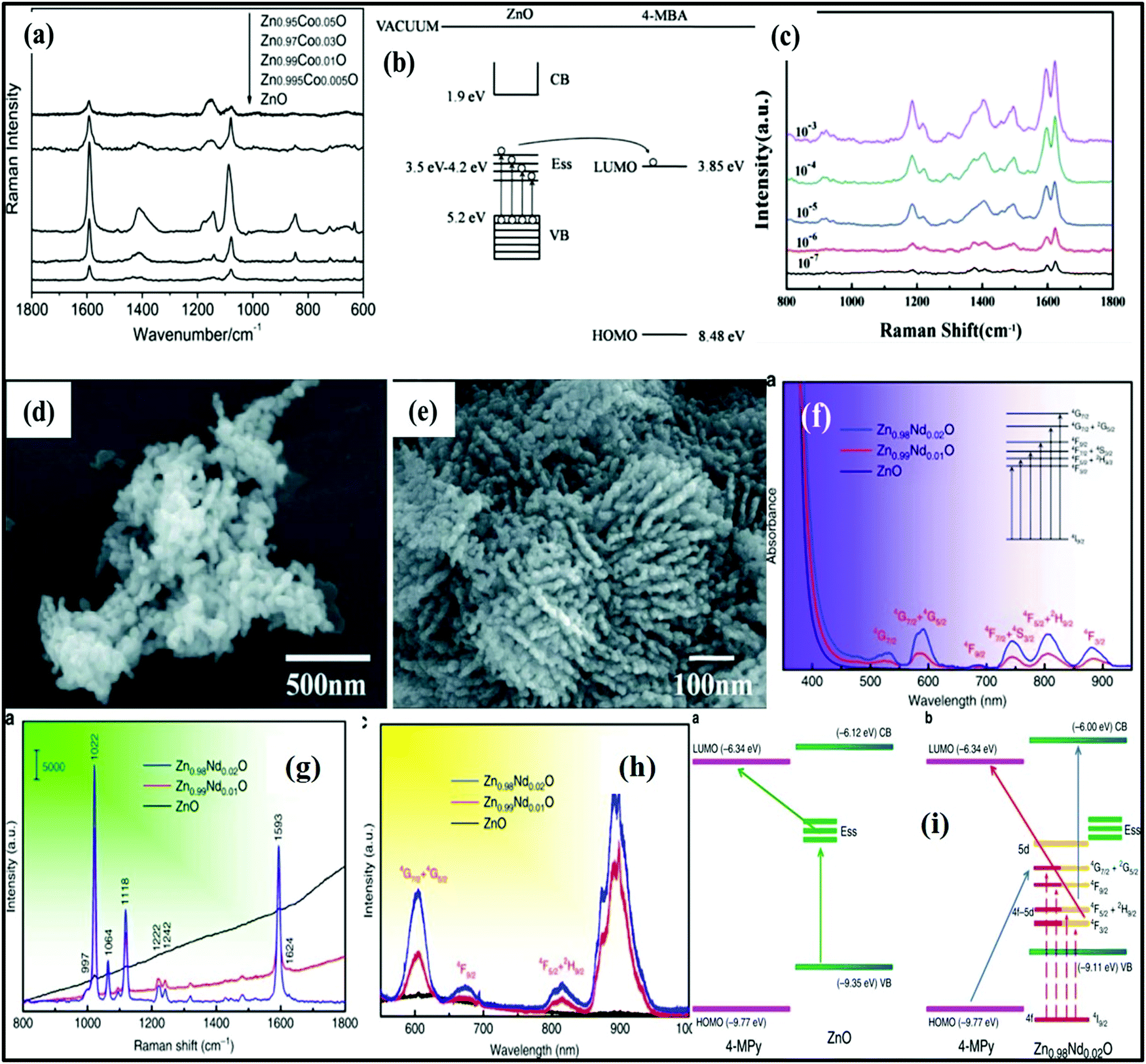 | ||
| Fig. 9 (a and b) SERS spectra with a 514.5 nm laser beam and CT process of pure and Co (0.5, 1, 3, and 5%) doped ZnO NPs. Copyright (2011) John Wiley and Sons. Used with permission from (X. Xue, W. Ruan, L. Yang, W. Ji, Y. Xie, L. Chen, W. Song, B. Zhao and J. R. Lombardi, Surface-enhanced Raman scattering of molecules adsorbed on Co-doped ZnO nanoparticles, J. Raman Spectrosc.).90 (c) SERS spectra of Malachite Green (MG) recorded using a laser with a wavelength of 514.5 nm based on Nd doped ZnO (ZNO) with concentrations ranging from 10−3 to 10−7 M. (d and e) SEM images of undoped and Nd doped ZnO. Reprinted with permission from [Springer Nature] [J. Mater. Sci.: Mater. Electron.] [ref. 62 M. Gao, J. Yao, Y. Quan, J. Yang, P. Huo, J. Dai, Y. Yan and C. Ma, Neodymium doped zinc oxide for ultrasensitive SERS substrate] Copyright (2019). (f–h) PL, SERS (recorded using a laser with a wavelength of 514 nm), and UV-vis absorption spectra of ZnO and Zn1−x Ndx O (x = 0.00, 0.01, 0.02), respectively, and (i) CT mechanisms between (a) 4-MPy and ZnO and (b) 4-MPy and Zn0.98Nd0.02O.96 | ||
Similar results were observed by Xue et al.91 in the case of Ni doping (0.00–0.05%) in ZnO. Due to their comparable size, Ni2+ ions were successfully substituted in the ZnO lattice causing defects acting as trapping centers for photoexcited electrons and facilitating the CT process. It was seen that, at 0.03% Ni doping, enhanced SERS performance was observed due to defect formation. Rare earth metals show narrow lines in intra-4f emission spectra which are attributed to the 4f electrons which are shielded by the outer 5s and 5p electrons. Thus, doping of rare earth metal ions in metal oxide semiconductor nanomaterials has been found to be an efficient method to enhance the SERS signal. For example, Gao et al.62 studied ultrasensitive detection of Malachite Green (MG) up to a concentration as low as 10−7 M with Nd doping in ZnO NPs as shown in Fig. 9(c). Fig. 9(d and e) shows changes in the morphology of the ZnO nanostructure before and after Nd doping. The Nd doping also decreased the size of doped ZnO NPs. It was observed that, at low doping concentrations, Nd3+ ions uniformly substituted in the ZnO lattice; however, as the concentration was increased, there was the formation of an oxide layer (Nd2O3) along with an increase in defect concentration as studied by Raman spectroscopy. These defects generated new energy levels below the CB and enhanced the CT process for higher SERS activity as compared to undoped ZnO. The enhancement factor of Nd doped ZnO nanostructures was found to be 7 times higher than that of the pure ZnO substrate.
Yang et al.96 conducted a detailed study and analysis of the relation between the SERS and PL spectra of Nd doped ZnO nanostructures as shown in Fig. 9(f–i). A change in the morphology of ZnO nanostructures was observed after doping from NPs to three dimensional (3D) urchin like nanostructures with improved optoelectronic and surface properties. Fig. 9(f) shows the UV absorption spectra, which indicated that, with doping, there is generation of some additional peaks corresponding to intra-4f shell transitions. The PL spectra (Fig. 9h) show that as the dopant concentration increases, there is an increase in the number of surface defects which facilitate the CT process. After doping there is a mixing of the empty 4f and 5d orbitals and formation of a 4f–5d orbital. Under light irradiation, the ground-state 4f electrons of Nd3+ ions excited to the higher empty 4f–5d levels and, under continuous irradiation, these excited electrons jump to the 5d levels. Overall, the CT channel originating from CT resonance overcomes the effect of 4f levels shielded by external 5s and 5p electrons as shown in Fig. 9(i).
Li et al.54 for the first time reported Ga doping in ZnO NPs explaining doping effects on the CT process. A series of ZnO NPs with varying Ga concentrations were prepared and their SERS activities against 4-MBA were studied. An increase in dopant concentration lowered the crystallinity and had no observable effect on the morphology of the samples. The UV absorption spectra showed a steep drop near 378 nm which was attributed to the CT process occurring between the VB and CB. Also, a considerable reduction occurred in band gap until the optimum Ga doping concentration reaches 6% and further increase in concentration increased the band gap. Raman spectra showed a new peak at 583 cm−1 corresponding to the oxygen vacancy, interstitial zinc, complex defects, etc. The decrease in the intensity of the main characteristic Raman peak with doping further confirmed the decrease in crystallinity. Doping caused shrinkage of band gap up to 0.08 eV by minimizing the gap between the VB and surface states which facilitated the CT process resulting in intense SERS signals.
Chang et al.89 described the synthesis of Al doped ZnO nanostructures by a simple chemical route and studied the effect of doping induced optimized ZnO nanostructures deposited with Ag nanoparticles which showed an excellent SERS effect. It was found that, before Ag deposition, an increase in Al doping concentration (2-5 mM aluminum sulfate) led to a change in ZnO morphology from nanoneedles to nanorods and finally ZnO nanosheets (Fig. 10a–d). It was concluded that Al doping exhibited a significant role in tailoring the ZnO nanoneedle structure for the deposited Ag nanoparticles to form a better ‘hot spot’ which contributed to the enhanced SERS signals. By means of Al doping and Ag deposition (by varying sputtering time) most enhanced SERS signals were observed up to the lowest detection limit of 10−10 M as shown in Fig. 10(e). Further increase in Ag concentration led to aggregation of Ag NPs which decreased the number of hot spots, resulting in decay of the SERS signals. Similarly, Al doping was engineered to tailor the ZnO@SnO2 heteronanowire structure/geometry most suitable for excellent SERS activity, followed by Ag deposition for an enhanced SERS effect.97 With the help of doping induced tailoring of the ZnO nanostructure and deposited Ag NPs, a lower concentration of R6G, i.e., up to 10−12 M, could be detected with high reproducibility and stability. Various doped ZnO nanostructures are listed in Table 1 with their SERS performance against various target molecules along with EF and other parameters.
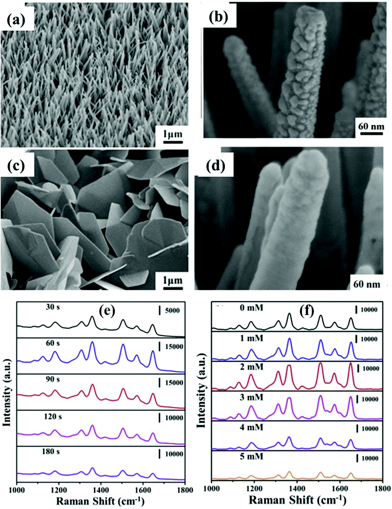 | ||
| Fig. 10 (a and c) SEM images of Al doped ZnO nanostructures fabricated at different concentrations of aluminum sulfate (2 and 5 mM). (b and d) SEM images of ZnO:Al (2 mM) nanoneedles deposited with Ag-sputtering at durations of 60 and 180 s, respectively. SERS spectra of R6G (10−6 M) on (e) ZnO:Al nanoneedles (2 mM aluminum sulfate) decorated with Ag nanoparticles at different sputtering times and (f) ZnO:Al nanoneedles at different Al concentrations decorated with Ag nanoparticles after Ag-sputtering for 60 s (using a laser with a wavelength of 532 nm). Reprinted from ref. 89, T.-H. Chang, Y.-C. Chang and S.-H. Wu, Ag nanoparticles decorated ZnO: Al nanoneedles as a high-performance surface-enhanced Raman scattering substrate, J. Alloys Compd., 843, 156044 Copyright (2020), with permission from Elsevier. | ||
4.3 Doping engineering of other metal oxide nanostructures for SERS applications
The effect of doping engineering using metals or non-metals for SERS applications has been mainly studied for TiO2 and ZnO nanostructures as discussed in the last section. Apart from these, there are a few other metal oxide semiconductor nanomaterials such as Ta2O5, WO3, MoO3, SnO2, ZrO2, etc. which have been used as SERS substrates and the effect of doping has been studied in view of a significant enhancement in their SERS activities.Lin et al.98 reported the SERS activity of Cu2O nanostructures for R6G molecules with an emphasis on the role of morphology. An EF of 8 × 10⁵ was observed using the Cu2O superstructure and found that the morphology plays an important role in improving SERS activity. Cu vacancies would produce a negatively charged Cu2O superstructure, which improved the adsorption of charged molecules, and enhanced the SERS performance. The synergistic effect of both surface defect and vacancy-induced electrostatic adsorption (EA) showed an excellent SERS enhancement. Lin et al.99 also studied three facets, namely, {100}, {110}, and {111}, of Cu2O NPs to investigate the facet-dependent SERS effect through theoretical investigation and found that the facets play an important role in the CT process. It was found that, among the three facets, {100} exhibited the lowest work function resulting in higher polarizability and therefore showed better CT properties. Due to the higher CT activity of the facet {100}, most of the electrons migrated from Cu2O microcrystals (MCs) to molecules and showed enhanced SERS signals as compared to the other facets. Yang et al.100 synthesized Nb2O5 nanoflowers wrinkled by nanosheets and studied the SERS performance of these flower nanostructures. These nanoflower structures formed by nanosheets had a large specific surface area, which facilitated the adsorption of more analyte molecules. In this case, SERS enhancement was reported as the synergistic effect of both EM and CT process. Under a laser beam with a wavelength of 532 nm, nanoflowers of Nb2O5 showed electromagnetic field enhancement (∼102) and strong CT resonance. After the adsorption of CV molecules on the Nb2O5 substrate, the UV spectra showed a shift towards the visible region, indicating the existence of the CT process. Peng et al.101 synthesized a novel recyclable SERS substrate of pure Nb2O5 and Mo doped Nb2O5 nanosheets by optimizing the hydrothermal reaction time from 24 to 72 h. Fig. 11(a and b) shows the SEM and HRTEM images of Mo doped Nb2O5 NPs. It was observed that a higher reaction time (72 h) provided Mo doped Nb2O5 NPs with an increased surface area which exhibited an excellent enhancement in Raman signals attributed to the fact that more analyte molecules were adsorbed on the surface. The enhancement factor was found to be 2.09 × 10⁷ with a detection limit of 10−8 M. Some of the selective peaks of methyl violet (MV) molecules were enhanced due to the bond formation between the molecule and substrate. Nb–C and Mo–C bonds were found to be responsible for the CT process in undoped Nb2O5 and Mo doped Nb2O5, respectively, as shown in Fig. 11(c). Furthermore, the synergistic effect of λlaser = λCT = λmol generated excellent CT, resulting in a strong Raman scattering signal (Fig. 11(d)).
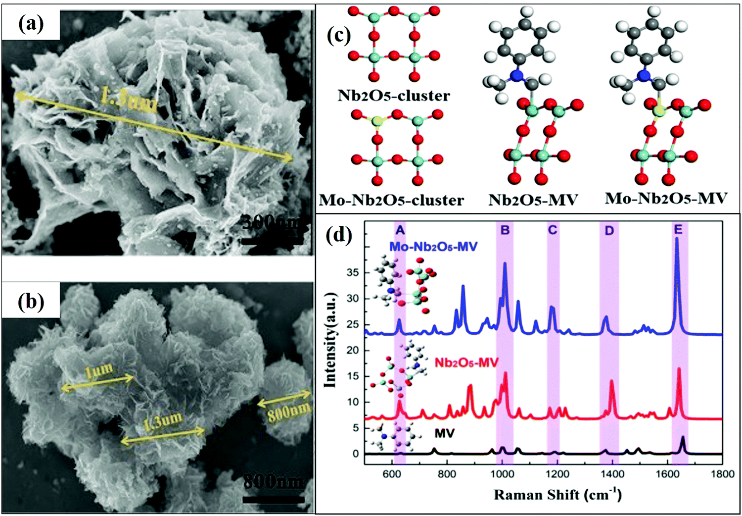 | ||
| Fig. 11 (a and b) TEM images of Nb2O5 and the Mo–Nb2O5 cluster. (c) Model of Nb2O5 and the Mo–Nb2O5 cluster, and Nb2O5–MV and Mo–Nb2O5–MV complexes. (d) SERS spectra of MV adsorbed on Nb2O5 and Mo–Nb2O5 (using a laser with a wavelength of 532 nm). Reprinted from ref. 101, Y. Peng, C. Lin, M. Tang, L. Yang, Y. Yang, J. Liu, Z. Huang and Z. Li, Niobium pentoxide ultra-thin nanosheets: a photocatalytic degradation and recyclable surface-enhanced Raman scattering substrate, Appl. Surf. Sci., 509, 145376, Copyright (2020), with permission from Elsevier. | ||
Yang et al.54 synthesized Mo doped and hydrogenated Ta2O5 metal oxide nanorods, respectively, by using a modified hydrothermal method. Fig. 12(a and b) shows the HRTEM image of uniformly synthesized nanorods. Fig. 12(c and d) present the schematic of the internal structure of Mo doped nanorods. The doping engineering was carried out using Mo which reduced the band gap energy of Ta2O5 as the ionic radii of Mo6+ (0.65 Å) and Ta5+ (0.64 Å) are similar and substitutional doping occurred. However, in the case of hydrogenated Ta2O5 crystals, hydrogen occupied the interlayer oxygen atoms, resulting in oxygen vacancies which contributed to the CT process. It was found that the polarizability of the target molecule also played an important role in SERS enhancement as 15% Mo doped Ta2O5 NRs showed the highest polarizability as compared to other doped Ta2O5 nanorods as shown in Fig. 12(e). The excitation wavelength of the laser (532 nm) well matched with the wavelength of Mo doped Ta2O5. The absorbance of the MV molecule also occurred in this region, and therefore λmol ≈ λCT ≈ λlaser, indicating that both CT and molecular resonance were found to be responsible for the higher enhancement in SERS signals as shown in Fig. 12(f). The 15% Mo doped Ta2O5 nanorods showed the highest SERS with an EF of 2.7 × 10⁷ and a sensitivity of 9 × 10⁻⁹ M for MV dye molecules.
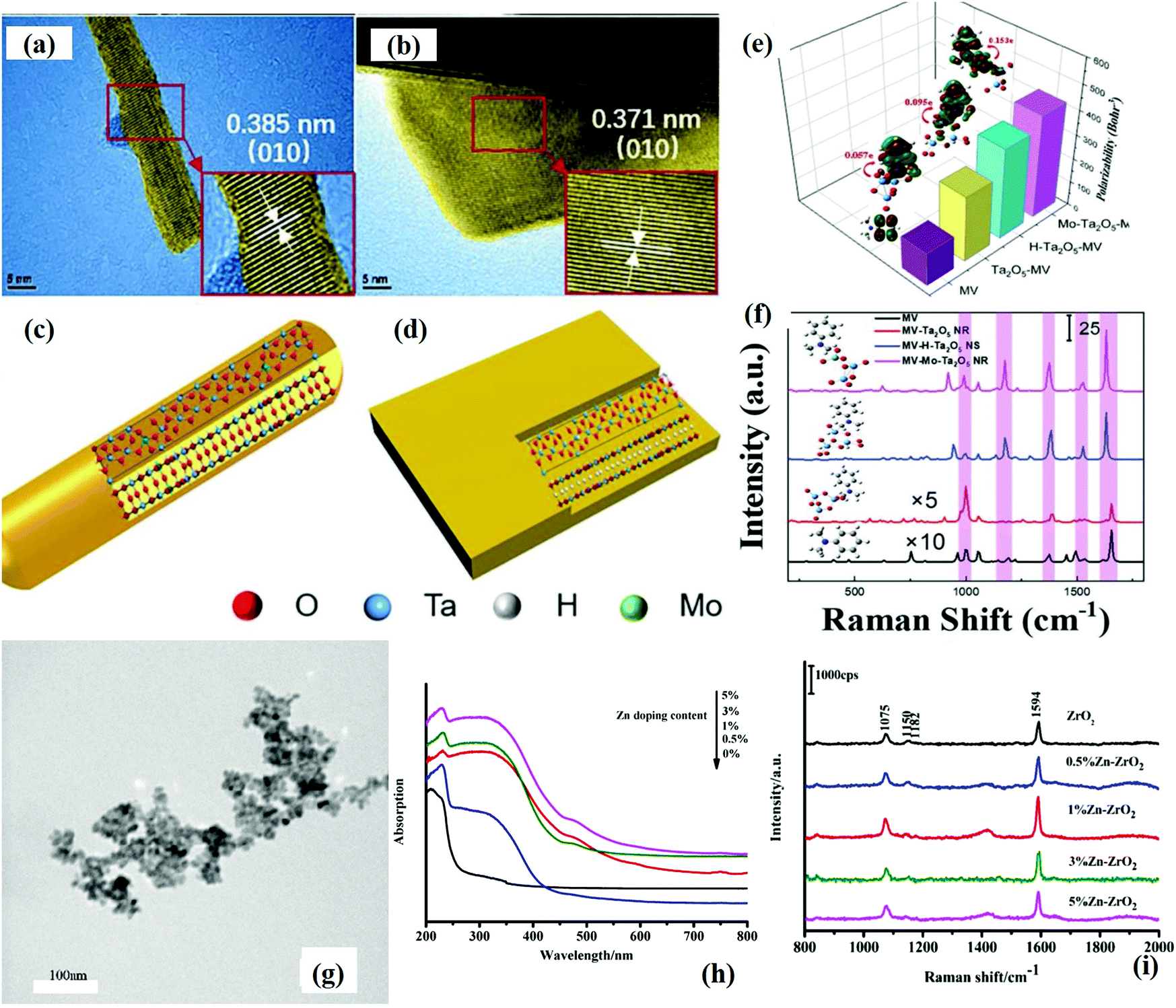 | ||
| Fig. 12 (a–d) HRTEM images and schematic diagrams for the crystal structures of Mo doped Ta2O5 clusters and H-Ta2O5 complexes. (e) SERS spectra (using a laser with a wavelength of 532 nm) of MV on different Ta2O5 substrates. (f) Calculated polarizabilities of single MV and MV adsorbed on Ta2O5 NR, H-Ta2O5, and Mo–Ta2O5, respectively.54 (g) SEM image of 1% Zn doped ZrO2. (h) UV and (i) SERS spectra (at a laser wavelength of 532 nm) of undoped and Zn doped ZrO2 NPs.102 | ||
Ji et al.103 studied the SERS activity of ZrO2 NPs by varying the calcination temperature. The ZrO2 NPs prepared by calcination at a temperature of 500 °C exhibited the highest SERS activity. It was found that ZrO2 NPs showed unprecedented Raman signal enhancements with an EF of 103 for 4-MBA, attributed to the plentiful surface defect state of the ZrO2 active substrate. Furthermore, it was found that an increase in calcination temperature led to the formation of highly crystalline ZrO2 NPs. It resulted in decreased surface defect levels which led to a decrease in the CT process and hence decreased SERS performance. Interestingly, in another study, Ji et al.102 studied the SERS activity of Zn doped ZrO2 NPs towards the detection of 4-MBA molecules as shown in Fig. 12(g–i). It was observed that, with an increase in Zn doping concentration, the absorbance maximum shifted to a higher wavelength, indicating a reduction in band gap (Fig. 12h). The absorbance spectra further confirmed the doping induced generation of defect levels below the CB of ZrO2 responsible for the enhanced CT process (as compared to pristine ZrO2). The 1% Zn doped ZrO2 NPs exhibited the highest SERS enhancement with an EF of 104 as shown in Fig. 12(i).
As discussed in Section 1, noble metals are most widely used as SERS substrates and show a maximum enhancement in the SERS signal. However, their use is limited due to some drawbacks as mentioned above. Recently, the effect of noble metal doping in metal oxide semiconductors has been studied to understand their role in the SERS performance of semiconductor nanomaterials. Juntaracena et al.104 synthesized Ag doped WO3 NFs and studied the SERS activity at different storage times of 6 and 12 months against MB molecules. The EFs for the freshly prepared sample and the sample stored for 6 and 12 months were estimated as 6.2 × 10⁵, 5.6 × 10⁵ and 1.7 × 10⁵, respectively. A decrease in the EF after 6 and 12 months was attributed to the agglomeration of Ag NPs, which declined the Raman enhancement effect when the samples were stored for a prolonged period.
There are limited studies showing the role of EM SERS enhancement in doped metal oxide semiconductors. Particularly, doping with electron rich dopants enables tuning of the LSPR of metal oxide semiconductors which contributes to SERS enhancement. Recently, Zhou et al.63 demonstrated the synthesis of MoO2 and S doped MoO2 hollow sphere substrates as shown in Fig. 13. The roles of morphology and S doping concentration (1–3 wt%) in tuning SERS signals were investigated. Doping of S in MoO2 was confirmed by XRD pattern analysis which showed some strain resulting from the replacement of O by S atoms. From the XPS spectra, it was found that S doping increased the charge on Mo atoms. The hollow sphere morphology with a large surface area facilitated the adsorption of analyte molecules and high light trapping as observed from the UV absorption spectra shown in Fig. 13(b). It was mentioned that electron rich S doping provided more electron density to the semiconductor, and when the laser light interacts with the free electrons, LSPR was generated. The S (2 wt%) doped MoO2 substrate exhibited a good detection sensitivity with a lower concentration up to the 10−10 M level, which was found to be comparable to noble metal detection as shown in Fig. 13(e and f). It was concluded that enhanced SERS activity with an EF of 6.2 × 10⁷ was observed which was attributed to the synergistic effect of both S doping and the distinct morphology of the MoO2 nanomaterial. Some important results regarding the SERS performance of metal oxide semiconductors other than TiO2 and ZnO are also listed in Table 1.
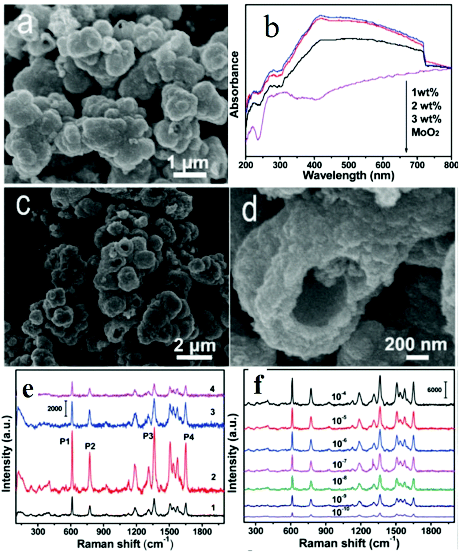 | ||
| Fig. 13 (a) SEM image of MoO2; (b) UV-vis absorption spectra of MoO2 and S doped MoO2; (c and d) SEM images of S-doped MoO2; (e) Raman signals of R6G (10−5 M) on (1) MoO2, (2) S-MoO2 (1 wt%), (3) S-MoO2 (2 wt%) and (4) S-MoO2 (3 wt%); (f) SERS signals of R6G with different concentrations on S-MoO2 (2 wt%) (SERS spectra were recorded using a laser with a wavelength of 532 nm).63 | ||
5. Doped metal oxide semiconductors as recyclable SERS substrates: the coexistence of photocatalytic degradation and SERS detection activity
Recyclable SERS active substrates are those that can detect the analyte molecules and photo-degrade them in order to re-use the substrates. Metal oxide-based SERS substrates have been widely used because of their excellent SERS activity and low toxicity; however, the precise detection of single molecules and reproducibility are still the matter of further research in this field. Metal oxide semiconductor based SERS substrates were modified by doping, making composites, etc. for achieving enhanced optical properties and a better SERS performance. Doped metal oxide-based SERS substrates have been considered as excellent bifunctional systems, i.e., detection and photocatalytic degradation of analyte molecules, which make them recyclable as shown in Fig. 14(a). Metal oxide semiconductors show self-cleaning ability which is very interesting for practical applications in which recycling of materials is desired.26,100,105–107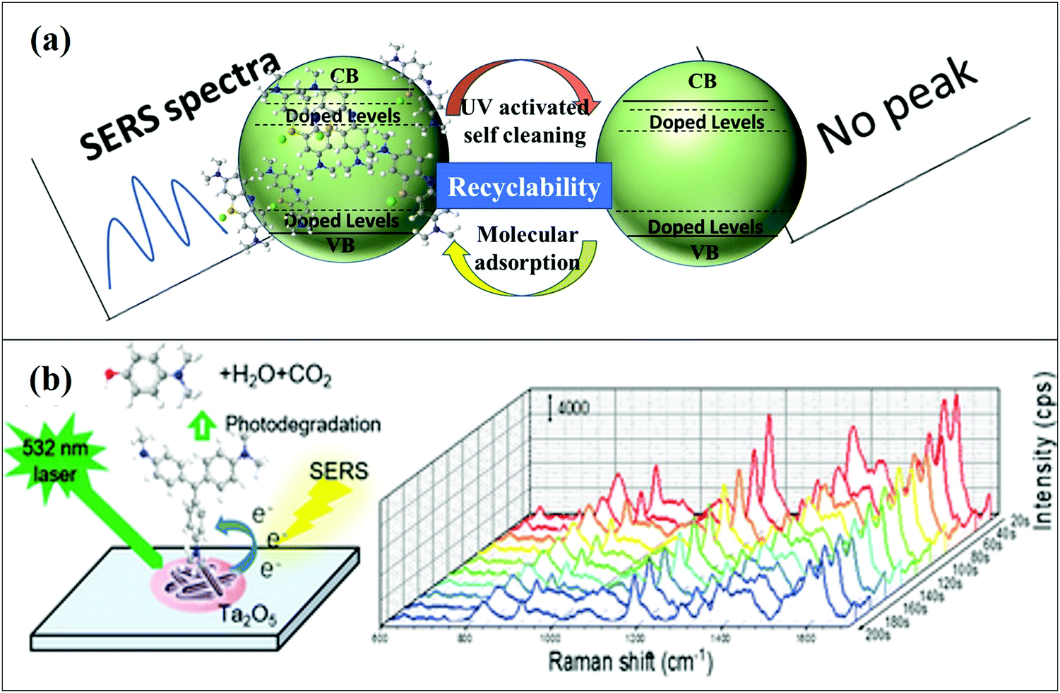 | ||
| Fig. 14 (a) Schematic showing the recyclable properties of doped metal oxide semiconductors. (b) SERS spectra of 10−6 m MV degraded on a 15%-Mo-Ta2O5 substrate under a laser with a 532 nm wavelength.54 | ||
As discussed in Section 3, doping can induce new doped energy levels in the metal oxide matrix which, by tuning the optical properties, facilitate the CT process and reduce the e−/h+ pair recombination, which results in improved SERS as well as photocatalytic activity as shown in Fig. 1(a). Metal oxide semiconductors (ZnO, TiO2, etc.) have a wide band gap which limits their photocatalytic activity. Doping with metals or non-metals creates sub-energy levels below the CB or above the VB and facilitates the photocatalytic process. Under irradiation with electromagnetic light, there is generation of electron (e−) and hole (h+) pairs (mainly in the UV region). These photogenerated e−/h+ pairs undergo chemical reactions with atmospheric oxygen and H2O, which leads to the formation of reactive oxygen species (ROS). These ROS react with organic pollutants and degrade them with the production of CO2 and H2O. This whole mechanism shows the self-cleaning properties of such metal oxide semiconductor photocatalysts which is very important for recycling of materials. For example, Durgam et al.107 studied the photocatalytic activity of metal ion-doped (Fe3+, Co2+, Ni2+ and Ag+) TiO2 nanocrystalline thin films. Doping causes narrowing of band gap energy and also the intensity of the emission spectra decreases which indicates a lower recombination rate of e−/h+ pairs after doping. The photodegradation activity of doped TiO2 towards MB and methyl orange (MO) dyes under visible light increased with doping. Among all dopants, i.e., Fe3+, Co2+, Ni2+ and Ag+, the photocatalytic activity of Ag+ ion-doped TiO2 was found to be excellent. Liu et al.108 reported improved photocatalytic activity of Fe doped ZnO NFs. Doping of Fe does not alter the morphology of NFs. However, the crystallite size and band gap energy decrease as the doping concentration increases. Due to the smaller band gap and crystallite size, the recombination rate of charge carriers decreases and the photocatalytic activity increases.
As discussed in Section 3, doping engineering of metal oxide semiconductors improves the CT process which further helps in enhancing the SERS signals of the analyte molecules. Metal oxide based SERS substrates show both ultra-sensitive SERS activity and cyclic photocatalytic activity via doping optimization. This type of multi-functional SERS substrate can simultaneously detect and degrade organic contaminants in the environment, making SERS substrates more environmentally friendly and cost-effective.
Peng et al.101 studied the recyclability of Mo doped Nb2O5 nanosheets. In this work, the MV dye was used to study the recyclability of SERS substrates. Laser light with a 532 nm wavelength was used for SERS detection of the molecule–substrate complex every 20 s. It was observed that the intensity of the Raman signal of the MV molecule decreased in inverse proportion to the laser radiation time. It was also observed that the MV molecules adsorbed on Mo–Nb2O5 substrates were photodegraded by visible light and exhibited excellent self-cleaning ability. Yang et al.54 studied the photodegradation of MV molecules which led to SERS signal decay on the photocatalytic semiconductor SERS substrate under the effect of a laser during SERS data collection. A 532 nm laser was used to collect the SERS signal every 20 s. From Fig. 14(b), it was observed that significant SERS signal attenuation occurred during laser irradiation at single-point SERS detection, attributed to the photoinduced degradation. It was suggested that shortening of irradiation time could be useful for obtaining better SERS signals and to avoid photoinduced degradation. Further, it was concluded that laser power was also a significant factor during the SERS measurement and photoinduced degradation of MV. With increasing laser power, enhanced SERS signals were recorded but it was found that with a very high laser power (50 mW) the SERS signal of MV could not be detected due to degradation or damage/change in the structure of the molecules.
Li et al.109 reported the bifunctionality of Ni doped TiO2 nanostructures such as SERS and photocatalytic activities. Ni doping in TiO2 enhanced the CT process and visible light absorption in TiO2 inverse opal nanostructures by tuning the optical properties. Ni doping in TiO2 nanostructures exhibited the SERS detection of 4-MBA molecules with a concentration as low as 1 × 10⁻¹¹ M and showed 95% degradation of MB under sunlight in 90 min. Similarly, Singh et al.26 studied the dual functionality of Ta doped TiO2 NFs. They reported that Ta doping created sub-energy levels below the CB which facilitated the CT process and also decreased the band gap energy, shifting the absorption maximum in the visible region. In view of the above discussion, it is mentioned that the recyclability of doped metal oxide semiconductors is very important for their real and long-term practical applications, which makes them unique. Doping further improves their optical properties which can contribute towards excellent SERS and photocatalytic activities.
6. Summary and future scopes
Metal oxide semiconductors act as excellent photocatalysts and SERS substrates due to their low cost, wide band gap, easy synthesis, tunable optical and morphological properties, high biocompatibility, and chemical/physical stability. However, due to their wide band gap and fast recombination of photogenerated charge carriers, the CT process is very weak, resulting in weak SERS activity of the adsorbed molecular species. In this review, the doping engineering strategy of metal oxide semiconductors has been discussed in detail to improve the CT process between the target molecule and metal oxide substrate for further enhancement of SERS sensitivity. Doping with metals or nonmetals generates new states below the CB of the metal oxide semiconductor, facilitates the CT process and shows an enhancement in the SERS signal comparable to noble metal substrates. This field has witnessed a lot of progress in the past decade with new exciting results competing with noble metal-based SERS substrates. However, there are a few challenges such as low EFs and very low detection limits compared to noble metal hybrid nanostructures and thus more systematic research is needed to explore the use of semiconductors in this filed. To improve the SERS activity of metal oxide semiconductors, further research needs to be conducted on new dopants from the periodic table, co-doping of elements, the effect of morphology, etc. We expect that this article will provide a better understanding and information to the research community and inspire researchers to explore the field with new advances.Conflicts of interest
There are no conflicts of interest to declare.Acknowledgements
The author (JP) thanks the Department of Science and Technology (DST), India, for the prestigious INSPIRE Faculty award [INSPIRE/04/2015/002452(IFA15-MS-57)] along with a research grant. Samriti and Vishal also acknowledge the National Institute of Technology Hamirpur for providing funding for their PhD and PG research work, respectively.References
- B. Sharma, R. R. Frontiera, A.-I. Henry, E. Ringe and R. P. Van Duyne, Mater. Today Chem., 2012, 15, 16–25 CrossRef CAS.
- E. L. Ru and P. Etchegoin, Principles of Surface-Enhanced Raman Spectroscopy: and related plasmonic effects, Elsevier, 2008 Search PubMed.
- J. Prakash, Int. Rev. Phys. Chem., 2019, 38, 201–242 Search PubMed.
- X. Tan, J. Melkersson, S. Wu, L. Wang and J. Zhang, ChemPhysChem, 2016, 17, 2630–2639 CrossRef CAS PubMed.
- A. Weber-Bargioni, A. Schwartzberg, M. Cornaglia, A. Ismach, J. J. Urban, Y. Pang, R. Gordon, J. Bokor, M. B. Salmeron and D. F. Ogletree, Nano Lett., 2011, 11, 1201–1207 CrossRef CAS PubMed.
- R. Zhang, Y. Zhang, Z. Dong, S. Jiang, C. Zhang, L. Chen, L. Zhang, Y. Liao, J. Aizpurua and Y. E. Luo, Nature, 2013, 498, 82–86 CrossRef CAS.
- M. Fleischmann, P. J. Hendra and A. J. McQuillan, Chem. Phys. Lett., 1974, 26, 163–166 CrossRef CAS.
- J. Langer, D. Jimenez de Aberasturi, J. Aizpurua, R. A. Alvarez-Puebla, B. Auguié, J. J. Baumberg, G. C. Bazan, S. E. Bell, A. Boisen and A. G. Brolo, ACS Nano, 2019, 14, 28–117 CrossRef PubMed.
- J. Prakash, R. Harris and H. Swart, Int. Rev. Phys. Chem., 2016, 35, 353–398 Search PubMed.
- J. Prakash, V. Kumar, R. Kroon, K. Asokan, V. Rigato, K. Chae, S. Gautam and H. Swart, Phys. Chem. Chem. Phys., 2016, 18, 2468–2480 RSC.
- D. Qi, L. Lu, L. Wang and J. Zhang, J. Am. Chem. Soc., 2014, 136, 9886–9889 CrossRef CAS.
- Z. Xie, F. Zhao, S. Zou, F. Zhu, Z. Zhang and W. Wang, J. Alloys Compd., 2021, 861, 157999 CrossRef CAS.
- J. Prakash, S. Sun, H. C. Swart and R. K. Gupta, Appl. Mater. Today, 2018, 11, 82–135 CrossRef.
- J. Prakash, V. Kumar, R. Kroon, K. Asokan, V. Rigato, K. Chae, S. Gautam and H. Swart, Phys. Chem. Chem. Phys., 2016, 18, 2468–2480 RSC.
- J. Prakash, S. Badilescu, R. Gupta, H. Swart, M. Packirisamy and S. Sun, Met. Nanopart., 2018, 125 Search PubMed.
- J. Langer, D. Jimenez de Aberasturi, J. Aizpurua, R. A. Alvarez-Puebla, B. Auguié, J. J. Baumberg, G. C. Bazan, S. E. Bell, A. Boisen and A. G. J. A. N. Brolo, ACS Nano., 2019, 14, 28–117 CrossRef PubMed.
- H. Zhang, R. An, X. Ji, Y. Dong, F. Pan, C. Liu and X. Lu, Chin. J. Chem. Eng., 2018, 26, 642–647 CrossRef CAS.
- I. Kriegel, F. Scotognella and L. Manna, Phys. Rep., 2017, 674, 1–52 CrossRef CAS.
- H. Wu, H. Wang and G. Li, Analyst, 2017, 142, 326–335 RSC.
- I. Alessandri and J. R. Lombardi, Chem. Rev., 2016, 116, 14921–14981 CrossRef CAS PubMed.
- J. Prakash, H. C. Swart, G. Zhang and S. Sun, J. Mater. Chem. C, 2019, 7, 1447–1471 RSC.
- L. Chen, H. Hu, Y. Chen, J. Gao and G. Li, Mater. Adv., 2021, 2, 907–926 RSC.
- X. X. Han, W. Ji, B. Zhao and Y. Ozaki, Nanoscale, 2017, 9, 4847–4861 RSC.
- D. Glass, E. Cortés, S. Ben-Jaber, T. Brick, W. J. Peveler, C. S. Blackman, C. R. Howle, R. Quesada-Cabrera, I. P. Parkin and S. A. Maier, Adv. Sci., 2019, 6, 1901841 CrossRef CAS.
- H. K. Lee, Y. H. Lee, C. S. L. Koh, G. C. Phan-Quang, X. Han, C. L. Lay, H. Y. F. Sim, Y.-C. Kao, Q. An and X. Y. Ling, Chem. Soc. Rev., 2019, 48, 731–756 RSC.
- N. Singh, J. Prakash, M. Misra, A. Sharma and R. K. Gupta, ACS Appl. Mater. Interfaces, 2017, 9, 28495–28507 CrossRef CAS PubMed.
- J. Prakash, A. Kumar, H. Dai, B. C. Janegitz, V. Krishnan, H. C. Swart and S. Sun, Mater. Today Sustain., 2021, 100066 CrossRef.
- D. Wan, Q. Wang, H. Huang, B. Jiang, C. Chen, Z. Yang, G. Li, C. Liu, X. Liu and L. Liao, Nanotechnology, 2021, 32, 135201 CrossRef CAS PubMed.
- J. Prakash, A. Singh, G. Sathiyan, R. Ranjan, A. Singh, A. Garg and R. K. Gupta, Mater. Today Energy, 2018, 9, 440–486 CrossRef.
- H. Yamada and Y. Yamamoto, Surf. Sci., 1983, 134, 71–90 CrossRef CAS.
- H. Ueba, Surf. Sci., 1983, 131, 347–366 CrossRef CAS.
- B. Yang, S. Jin, S. Guo, Y. Park, L. Chen, B. Zhao and Y. M. Jung, ACS Omega, 2019, 4, 20101–20108 CrossRef CAS PubMed.
- X. Wang and L. Guo, Angew. Chem., Int. Ed., 2020, 59, 4231–4239 CrossRef CAS PubMed.
- Y. Zhao, H. Pan, Y. Lou, X. Qiu, J. Zhu and C. Burda, J. Am. Chem. Soc., 2009, 131, 4253–4261 CrossRef CAS PubMed.
- W. Li, R. Zamani, P. Rivera Gil, B. Pelaz, M. Ibáñez, D. Cadavid, A. Shavel, R. A. Alvarez-Puebla, W. J. Parak and J. Arbiol, J. Am. Chem. Soc., 2013, 135, 7098–7101 CrossRef CAS PubMed.
- J. Zheng, B. Dai, J. Liu, J. Liu, M. Ji, J. Liu, Y. Zhou, M. Xu and J. Zhang, ACS Appl. Mater. Interfaces, 2016, 8, 35426–35434 CrossRef CAS PubMed.
- X. J. F. i. M. Liu, Front. Mater., 2018, 5, 59 CrossRef.
- J. Prakash, S. Sun, H. C. Swart and R. K. Gupta, Appl. Mater. Today, 2018, 11, 82–135 CrossRef.
- Y. S. Yamamoto and T. Itoh, J. Raman Spectrosc., 2016, 47, 78–88 CrossRef CAS.
- A. Agrawal, S. H. Cho, O. Zandi, S. Ghosh, R. W. Johns and D. J. Milliron, Chem. Rev., 2018, 118, 3121–3207 CrossRef CAS.
- A. Agrawal, R. W. Johns and D. J. Milliron, Annu. Rev. Mater. Res., 2017, 47, 1–31 CrossRef CAS.
- J. A. Faucheaux, A. L. Stanton and P. K. Jain, J. Phys. Chem. Lett., 2014, 5, 976–985 CrossRef CAS.
- B. Balasubramaniam, N. Singh, P. Kar, A. Tyagi, J. Prakash and R. K. Gupta, Mol. Syst. Des. Eng., 2019, 4, 804–827 RSC.
- P. Luo, F. Zhuge, Q. Zhang, Y. Chen, L. Lv, Y. Huang, H. Li and T. Zhai, Nanoscale Horiz., 2019, 4, 26–51 RSC.
- J. Prakash, P. Kumar, R. Harris, C. Swart, J. Neethling, A. J. van Vuuren and H. Swart, Nanotechnology, 2016, 27, 355707 CrossRef.
- J. Prakash, R. Harris and H. Swart, Int. Rev. Phys. Chem., 2016, 35, 353–398 Search PubMed.
- J. Langer, D. Jimenez de Aberasturi, J. Aizpurua, R. A. Alvarez-Puebla, B. Auguié, J. J. Baumberg, G. C. Bazan, S. E. Bell, A. Boisen and A. G. Brolo, ACS Nano, 2019, 14, 28–117 CrossRef PubMed.
- L. Lan, Y. Gao, X. Fan, M. Li, Q. Hao and T. Qiu, Front. Phys., 2021, 16, 1–26 Search PubMed.
- T. Gupta, J. Cho and J. Prakash, Mater. Today Chem., 2021, 20, 100428 CrossRef CAS.
- I. Alessandri and J. R. Lombardi, Chem. Rev., 2016, 116, 14921–14981 CrossRef CAS PubMed.
- D. Maznichenko, K. Venkatakrishnan and B. Tan, J. Phys. Chem. C, 2013, 117, 578–583 CrossRef CAS.
- J. M. Luther, P. K. Jain, T. Ewers and A. P. Alivisatos, Nat. Mater., 2011, 10, 361–366 CrossRef CAS.
- J. R. Lombardi and R. L. Birke, J. Phys. Chem. C, 2014, 118, 11120–11130 CrossRef CAS.
- L. Yang, Y. Peng, Y. Yang, J. Liu, H. Huang, B. Yu, J. Zhao, Y. Lu, Z. Huang and Z. Li, Adv. Sci., 2019, 6, 1900310 CrossRef.
- W. Ji, L. Li, W. Song, X. Wang, B. Zhao and Y. Ozaki, Angew. Chem., Int. Ed., 2019, 58, 14452–14456 CrossRef CAS.
- I. Alessandri, J. Am. Chem. Soc., 2013, 135, 5541–5544 CrossRef CAS PubMed.
- H. Kim, K. M. Kosuda, R. P. Van Duyne and P. C. Stair, Chem. Soc. Rev., 2010, 39, 4820–4844 RSC.
- J. R. Lombardi and R. L. Birke, J. Phys. Chem. C, 2008, 112, 5605–5617 CrossRef CAS.
- D. R. Maslennikov, A. Y. Sosorev, R. S. Fedorenko, Y. N. Luponosov, S. A. Ponomarenko and V. V. Bruevich, J. Phys. Chem. C, 2019, 123, 27242–27250 CrossRef CAS.
- J. R. Lombardi, Faraday Discuss., 2017, 205, 105–120 RSC.
- X. Xue, W. Ji, Z. Mao, Z. Li, W. Ruan, B. Zhao and J. R. Lombardi, Spectrochim. Acta, Part A, 2012, 95, 213–217 CrossRef CAS.
- M. Gao, J. Yao, Y. Quan, J. Yang, P. Huo, J. Dai, Y. Yan and C. Ma, J. Mater. Sci.: Mater. Electron., 2019, 30, 20537–20543 CrossRef CAS.
- X. Zhou, X. Zhao, S. Gu, F. Xie, X. Wang and Z. Tang, Anal. Methods, 2021, 13, 2679–2687 RSC.
- L. Yang, X. Jiang, W. Ruan, B. Zhao, W. Xu and J. R. Lombardi, J. Phys. Chem. C, 2008, 112, 20095–20098 CrossRef CAS.
- L. Yang, M. Gong, X. Jiang, Y. Chen, X. Han, K. Song, X. Sun, Y. Zhang and B. Zhao, Colloids Surf., A, 2016, 508, 142–149 CrossRef CAS.
- H. Hu, Z. Shi, K. Khan, R. Cao, W. Liang, A. K. Tareen, Y. Zhang, W. Huang, Z. Guo and X. Luo, J. Mater. Chem. A, 2020, 8, 5421–5441 RSC.
- L. Yang, M. Gong, X. Jiang, Y. Chen, X. Han, K. Song, X. Sun, Y. Zhang and B. Zhao, Colloids Surf., A, 2016, 508, 142–149 CrossRef CAS.
- A. Sreedhar, J. H. Kwon, J. Yi, J. S. Kim and J. S. Gwag, Mater. Sci. Semicond. Process., 2016, 49, 8–14 CrossRef CAS.
- M. Jing, R. Hong, W. Wei, C. Tao, D. Zhang and S. Zhuang, Opt. Mater., 2017, 73, 371–376 CrossRef CAS.
- V. Đorđević, B. Milićević and M. D. Dramićanin, Titanium Dioxide, Intech Open, London, 1st edn, 2017, pp. 25–60 Search PubMed.
- M. Achehboune, M. Khenfouch, I. Boukhoubza, B. M. Mothudi, I. Zorkani and A. Jorio, J. Mater. Sci.: Mater. Electron., 2020, 31, 4595–4604 CrossRef CAS.
- M. Meksi, G. Berhault, C. Guillard and H. Kochkar, Catal. Commun., 2015, 61, 107–111 CrossRef CAS.
- X. Jiang, K. Song, X. Li, M. Yang, X. Han, L. Yang and B. S. Zhao, ChemistrySelect, 2017, 2, 3099–3105 CrossRef CAS.
- C. Di Valentin and G. Pacchioni, Catal. Today, 2013, 206, 12–18 CrossRef CAS.
- C. Di Valentin and G. Pacchioni, Acc. Chem. Res., 2014, 47, 3233–3241 CrossRef CAS PubMed.
- P. A. K. Reddy, P. V. L. Reddy, E. Kwon, K.-H. Kim, T. Akter and S. Kalagara, Environ. Int., 2016, 91, 94–103 CrossRef CAS PubMed.
- L. Yang, X. Jiang and M. Yang, Appl. Phys. Lett., 2011, 99, 111114 CrossRef.
- B. Niu, X. Wang, K. Wu, X. He and R. Zhang, Mater. Today Chem., 2018, 11, 1910 Search PubMed.
- X. Xue, W. Ji, Z. Mao, H. Mao, Y. Wang, X. Wang, W. Ruan, B. Zhao and J. R. Lombardi, J. Phys. Chem. C, 2012, 116, 8792–8797 CrossRef CAS.
- L. Yang, M. Gong, X. Jiang, D. Yin, X. Qin, B. Zhao and W. Ruan, J. Raman Spectrosc., 2015, 46, 287–292 CrossRef CAS.
- L. Yang, X. Jiang, W. Ruan, B. Zhao, W. Xu and J. R. Lombardi, J. Raman Spectrosc., 2009, 40, 2004–2008 CrossRef CAS.
- L. Yang, Y. Zhang, W. Ruan, B. Zhao, W. Xu and J. R. Lombardi, J. Raman Spectrosc., 2010, 41, 721–726 Search PubMed.
- X.-x. Xue, W. Ji, Z. Mao, Z.-s. Li, Z.-n. Guo, B. Zhao and C. Zhao, Chem. Res. Chin. Univ., 2013, 29, 751–754 CrossRef CAS.
- X. Xue, W. Ji, Z. Mao, C. Zhao, B. Zhao and J. R. Lombardi, RSC Adv., 2013, 3, 20891–20895 RSC.
- M. Jing, R. Hong, W. Wei, C. Tao, D. Zhang and S. Zhuang, Opt. Mater., 2017, 73, 371–376 CrossRef CAS.
- V. Kiran and S. Sampath, ACS Appl. Mater. Interfaces, 2012, 4, 3818–3828 CrossRef CAS PubMed.
- J. Theerthagiri, S. Salla, R. Senthil, P. Nithyadharseni, A. Madankumar, P. Arunachalam, T. Maiyalagan and H.-S. Kim, Nanotechnology, 2019, 30, 392001 CrossRef CAS PubMed.
- F. Rahman, Opt. Eng., 2019, 58, 010901 CAS.
- T.-H. Chang, Y.-C. Chang and S.-H. Wu, J. Alloys Compd., 2020, 843, 156044 CrossRef CAS.
- X. Xue, W. Ruan, L. Yang, W. Ji, Y. Xie, L. Chen, W. Song, B. Zhao and J. R. Lombardi, J. Raman Spectrosc., 2012, 43, 61–64 CrossRef CAS.
- X. Xue, J. Zhang, L. Chen, C. Zhao, L. Wang and L. Chang, J. Nanosci. Nanotechnol., 2018, 18, 4403–4408 CrossRef CAS PubMed.
- Z. Sun, B. Zhao and J. R. Lombardi, Appl. Phys. Lett., 2007, 91, 221106 CrossRef.
- Q. Liu, L. Jiang and L. Guo, Small, 2014, 10, 48–51 CrossRef CAS PubMed.
- H.-Y. Shin, E.-L. Shim, Y.-J. Choi, J.-H. Park and S. Yoon, Nanoscale, 2014, 6, 14622–14626 RSC.
- X. Wang, W. Shi, Z. Jin, W. Huang, J. Lin, G. Ma, S. Li and L. Guo, Angew. Chem., 2017, 129, 9983–9987 CrossRef.
- S. Yang, J. Yao, Y. Quan, M. Hu, R. Su, M. Gao, D. Han and J. Yang, Light: Sci. Appl., 2020, 9, 1–7 CrossRef CAS PubMed.
- Y.-C. Chang and S.-H. Wu, J. Ind. Eng. Chem., 2019, 76, 333–343 CrossRef CAS.
- J. Lin, Y. Shang, X. Li, J. Yu, X. Wang and L. Guo, Adv. Mater., 2017, 29, 1604797 CrossRef PubMed.
- J. Lin, W. Hao, Y. Shang, X. Wang, D. Qiu, G. Ma, C. Chen, S. Li and L. Guo, Small, 2018, 14, 1703274 CrossRef PubMed.
- L. Yang, Y. Wei, Y. Song, Y. Peng, Y. Yang and Z. Huang, Mater. Des., 2020, 193, 108808 CrossRef CAS.
- Y. Peng, C. Lin, M. Tang, L. Yang, Y. Yang, J. Liu, Z. Huang and Z. Li, Appl. Surf. Sci., 2020, 509, 145376 CrossRef CAS.
- P. Ji, Z. Mao, Z. Wang, X. Xue, Y. Zhang, J. Lv and X. Shi, Nanomaterials, 2019, 9, 983 CrossRef CAS PubMed.
- P. Ji, Z. Wang, X. Shang, Y. Zhang, Y. Liu, Z. Mao and X. Shi, Front. Chem., 2019, 7, 245 CrossRef CAS PubMed.
- K. Juntaracena, T. Yuangkaew, M. Horprathum, N. Triroj and P. Jaroenapibal, Vib. Spectrosc., 2021, 103276 CrossRef CAS.
- X. Wang, L. Zhou, W. Lai, T. Jiang and J. Zhou, Phys. Chem. Chem. Phys., 2016, 18, 23795–23802 RSC.
- J. Prakash, Int. Rev. Phys. Chem., 2019, 38, 201–242 Search PubMed.
- K. Durgam, R. Eppa and R. R. Mv, Surf. Interface Anal., 2021, 53, 194–205 CrossRef CAS.
- L. Liu, Z. Liu, Y. Yang, M. Geng, Y. Zou, M. B. Shahzad, Y. Dai and Y. Qi, Ceram. Int., 2018, 44, 19998–20005 CrossRef CAS.
- X. Li, Y. Wu, Y. Shen, Y. Sun, Y. Yang and A. Xie, Appl. Surf. Sci., 2018, 427, 739–744 CrossRef CAS.
| This journal is © The Royal Society of Chemistry 2022 |