
Semitransparent organic solar cells: from molecular design to structure–performance relationships
Kanupriya
Khandelwal
 a,
Subhayan
Biswas
a,
Amaresh
Mishra
*b and
Ganesh D.
Sharma
*a
a,
Subhayan
Biswas
a,
Amaresh
Mishra
*b and
Ganesh D.
Sharma
*a
aDepartment of Physics, The LNM Institute of Information Technology (Deemed University), Rupa ki Nagal, Jamdoli, Jaipur, Rajasthan – 302031, India. E-mail: gdsharma273@gmail.com; gdsharma@lnmiit.ac.in
bSchool of Chemistry, Sambalpur University, Jyoti Vihar – 768019, Sambalpur, India. E-mail: amaresh.mishra@suniv.ac.in
First published on 18th November 2021
Abstract
Organic solar cells (OSCs) have drawn tremendous interest because of their potential for low-cost solution processing and color tunability. OSCs with bulk-heterojunction structures offer an attractive pathway to efficiently utilize solar energy and have the potential to make transparent and flexible devices. The design of new materials and optimized device fabrications with visible-light transparency make this technology attractive for various applications, including greenhouses, windows, building structures, etc. In this review, we highlight the developments of fullerene-free acceptors (FFAs) for semitransparent OSCs (ST-OSCs) and device architectures, including transparent electrodes, giving special emphasis to the power conversion efficiency (PCE) and the average visible transparency (AVT).
 Kanupriya Khandelwal | Kanupriya Khandelwal is a PhD Scholar in the Department of Physics at The LNM Institute of Information Technology, Jaipur, India, under the supervision of Prof. Ganesh D. Sharma and Dr Subhayan Biswas. Her main research interests are in the optoelectronic properties of organic materials for applications in photovoltaic devices. She is currently working on the semitransparent organic solar cells and its BIPV (Building Integrated Photovoltaics) application. |
 Subhayan Biswas | Dr Subhayan Biswas is an associate professor in the Department of Physics at The LNM Institute of Information Technology, Jaipur, India. After completing PhD from the Indian Association for the Cultivation of Science, Kolkata, India, he did post-doctoral research in Inha University (South Korea), National Sun Yat-Sen University & National Taiwan University (Taiwan) and Toyama University (Japan). His research field is nanostructured solar cells including dye-sensitized solar cells, quantum-dot solar cells and organic solar cells. |
 Amaresh Mishra | Dr Amaresh Mishra is an Associate Professor at the School of Chemistry, Sambalpur University, India. He received his PhD in 2000 from Sambalpur University. After a postdoctoral stay at the University of South Florida and University of Akron from 1999–2001, he joined TIFR, Mumbai, India as a Visiting Fellow. He then moved to University of Ulm, Germany in 2005, as Alexander von Humboldt Fellow and continued there to lead the organic solar cells research group till 2015. His current research focuses on the design and development of functional organic semiconductors and hybrid materials for photovoltaic applications. |
 Ganesh D. Sharma | Prof. Ganesh D. Sharma is working as Senior Professor of Physics, Electronics Communication and Engineering and Dean (Research and development) at The LNM Institute of Information Technology, Jaipur (Raj.), India since Dec 2014. Prof. Sharma obtained his PhD degree from India Institute of Technology in 1985 and after than he had joined as Assistant Professor at JNV University, Jodhpur (Raj), India and subsequently as Professor. His area of Research is Organic solar cells, nanocrystalline organic–inorganic hybrid solar cells and fuel cells, organic nanomaterials for energy conversion and published more than 320 research papers. He had research collaborations with different International and National research organization. |
1. Introduction
Globally, energy is one of the crucial parameters for sustainability and socio-economic growth. At present, a significant part of the energy requirements is fulfilled by using non-renewable fossil fuels which cause irreparable damage to the environment. It is clear that the structure of energy demand is likely to change over time with the decline in use of fossil fuels and the increasing demand for renewable energy. So, exploiting clean and green renewable energy resources is necessary to fulfill the global energy demand. In this respect, solar energy as an alternative to fossil fuels has been considered as a renewable energy source to meet the energy needs of society.1,2 Photovoltaics that can convert solar energy directly into electricity hold promise for cost-effective solar cells prepared via simple solution-processing. Among the photovoltaic technologies, organic solar cells (OSCs) have emerged as a convincing technology because of their numerous advantages, such as new molecular design, tunable device structure, fabrication on flexible substrates, and transparency. Building-integrated photovoltaic (BIPV) devices are architecturally integrated on the rooftops/facades of commercial and residential buildings as an added function to produce electricity.3–7 Thus, the BIPV system simultaneously serves as a building envelope material to improve the aesthetic appearance due to color transparency and as a source for power generation.Organic materials with a high absorption coefficient (∼105 cm−1) and a tunable bandgap have tremendous potential to be used in semitransparent solar cells (ST-OSCs) due to their variable absorption from the visible to the near-IR regions, leaving some transparent windows in the visible region.8,9 They have the advantages of flexibility, being solution-processable and suitable for large-scale roll-to-roll fabrication.10–13 ST-OSCs have become the stronger contender for BIPV devices and are believed to be an effective solution for balancing energy generation with visual eye comfort and a pleasant appearance.14–18 The transparency in ST-OSCs can be maintained by reducing the thickness of the organic photoactive layers, by choosing appropriate transparent bottom or top electrodes and matching energetics, and by maintaining a high power conversion efficiency (PCE) and an average visible transmittance (AVT).19 In the past few years, the PCE of single-junction OSCs has increased significantly, up to 18%, using either binary or ternary blends (Fig. 1a).20–24 The only difference between the opaque OSCs and ST-OSCs is the device transparency in the visible region. There is an inherent trade-off between the PCE and AVT, so a balance between these two crucial factors is necessary (Fig. 1b). The AVT of ST-OSCs using fullerene acceptors and wide bandgap donors is quite low due to the relatively broad photon harvesting in the visible-light range. Due to the diversity in organic light-absorbing materials and specifically after the development of fullerene-free acceptors (FFAs) that absorb in the visible to NIR regions, ST-OSCs can be engineered in various colors.16,25 The NIR-absorbing FFAs play a key role to enhance the transmittance of ST-OSCs with increasing PCE. Because of their aesthetic advantages, flexibility, and low cost, ST-OSCs have become a strong contender for BIPV applications. ST-OSCs have been intensively studied in recent years, and the PCE has increased from ∼2% to 13% with outstanding AVT values for windows applications.15,18 These improvements are due to the rapid development in high-performance photoactive materials, the judicious choice of transparent bottom and top electrodes, and to the low-temperature-processable interface layer.
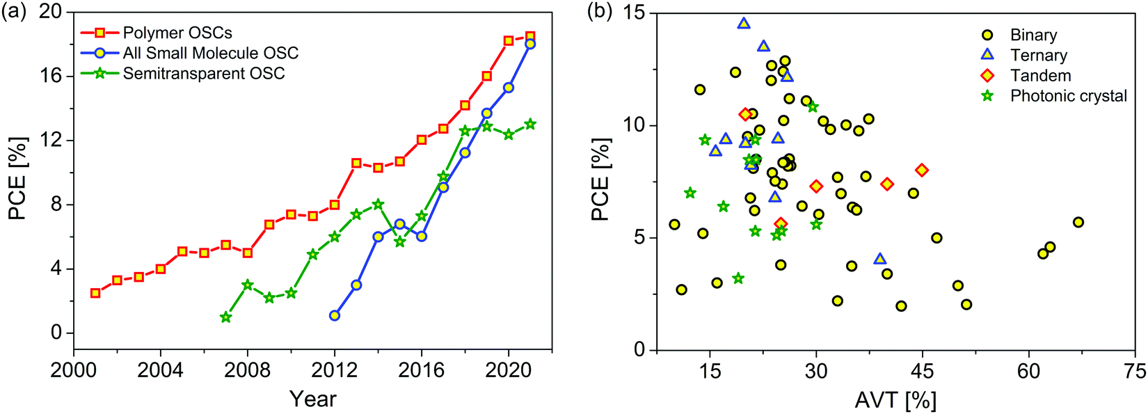 | ||
| Fig. 1 (a) Progress in organic solar cell efficiencies over the years. (b) Comparative plot of PCEs versus AVTs as discussed in this article and presented in Tables 1–3. | ||
Dye-sensitized solar cells (DSSCs) are another photovoltaic system for BIPV applications and offer high transparency and AVT (>80%) at micron-level thicknesses (10–20 nm TiO2 NPs).26–30 However, due to the liquid nature of the materials utilized in DSSCs, poor charge transmission and leakage problems pose a hurdle to their practical use. Singh and co-workers reported a semitransparent DSSC using a NIR-absorbing squaraine-based sensitizer.31 Recently, Naim et al. reported a colorless transparent DSSC using a polymethine cyanine dye that achieved a PCE of 3.1% and an AVT close to 76%.32 Mini modules with an active area of 14 cm2 based on organic dyes have been reported with a PCE of 8.7% and an AVT of 26%.33 In a very short period the field of perovskite solar cells (PSCs) based on organic–inorganic hybrid metal halides has emerged as a promising source of energy-harvesting materials, which are considered to be a suitable alternative to DSSCs, with PCE values reaching over 22%.34–36 The absorption, bandgap and thickness of perovskite films can be easily tuned to achieve visible transparency for ST-PSCs. The major difference between a ST-PSC and a ST-OSC is the photoactive layer.37–39 The perovskite materials generally absorb strongly in the visible region, therefore, the thickness must be reduced to achieve semitransparency. Using a thin film of CH3NH3PbI3 perovskite, Bolink and co-workers achieved a PCE of 6% with an AVT close to 29%.40 Li and co-workers realized a ST-PSC by increasing the bromine content in the CH3PbI3−xBrx perovskite to tune the bandgap and achieved a transparency of 20%.41 Snaith's group reported microporous layers of neutral-color CH3NH3PbI3 perovskite films using a partial dewetting method, achieving PCEs of 8–4% and AVTs of 7–30%.42 Color-tunable ST-PSCs were also reported by tuning the optical methods, i.e., using a metal/dielectric/metal electrode without disturbing the perovskite film.43,44 Chen et al. prepared a macroporous CH3NH3PbI3 perovskite film by modifying the polystyrene microsphere template, reaching a high AVT of 36.5% with an impressive PCE of 11.7%.45
In this review, we present a brief description of the current status in molecular design for ST-OSCs and deduce the structure–performance relationships for a BIPV or power-generating window and greenhouse applications. We further discuss the challenges and future research direction for ST-OSCs, providing ideas for new technologies.
2. Basic characterizations of semitransparent OSCs
In our daily life, there has always been a significant impact of the solar light that passes through the transparent windows of buildings and houses on the visual comfort of the human eye. Semitransparent OSCs are considered to be an effective approach to balancing the visual comfort of the eyes whilst simultaneously generating energy in glass buildings and windows. ST-OSCs also offer an aesthetic color selection that enables natural colors to be seen through windows. For optimizing ST-OSCs three critical parameters, such as the AVT, color perception transparency, and color rendering index (CRI), should be considered along with the PCE. The PCE is determined from PCE = (JSC × VOC × FF)/Pin, where JSC is the short-circuit current density, VOC is the open-circuit voltage, FF is the fill factor and Pin is the incident light power. Transparency is a very important factor in ST-OSCs and is usually assessed by calculating the AVT in the visible region from 400–780 nm. Although the AVT requirement is based on real applications, it is considered that an AVT of 25% is a minimum requirement for window applications.46 While measuring the transmittance, the light beam should be focused within the device's active area.47 The AVT can be calculated using the equation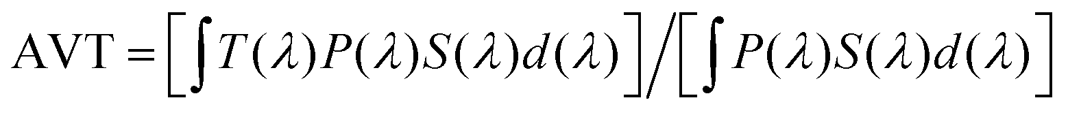 , where T(λ) is the transmittance spectrum, P(λ) is the human eye photopic response, and S(λ) is the solar photon flux (AM 1.5) for window applications.
Color perception is a parameter determined via the International Lighting Commission (CIE) 1931 xy chromaticity to estimate the transparency. AM1.5G and D65 are the commonly used reference light sources for estimating the color properties of ST-OSCs with the color coordinates of (0.3202,0.3324) and (0.3128,0.3290), respectively (Fig. 2). For window applications, the color coordinates of ST-OSCs are preferably close to the white point (0.333,0.333). Ameri et al. first introduced the concept of the chromaticity diagram for analyzing the color properties of ST-OSCs.48 The color rendering index (CRI) is another parameter that measures how well a light source can expose an object's color when compared with a reference or natural source of light. The human eye has an amazing ability to adapt to color variations induced by different lighting situations. The CRI in ST-OSCs represents the degree of color rendering variance between the incident and the transmitted light, and a higher CRI means a better color-rendering ability. For power-generating window applications, a CRI value close to 100 has been approved.49 The use of a dielectric/metal/dielectric (DMD) as the top electrode in ST-OSCs has been found to reach a CRI value close to 100 without sacrificing the performance.50
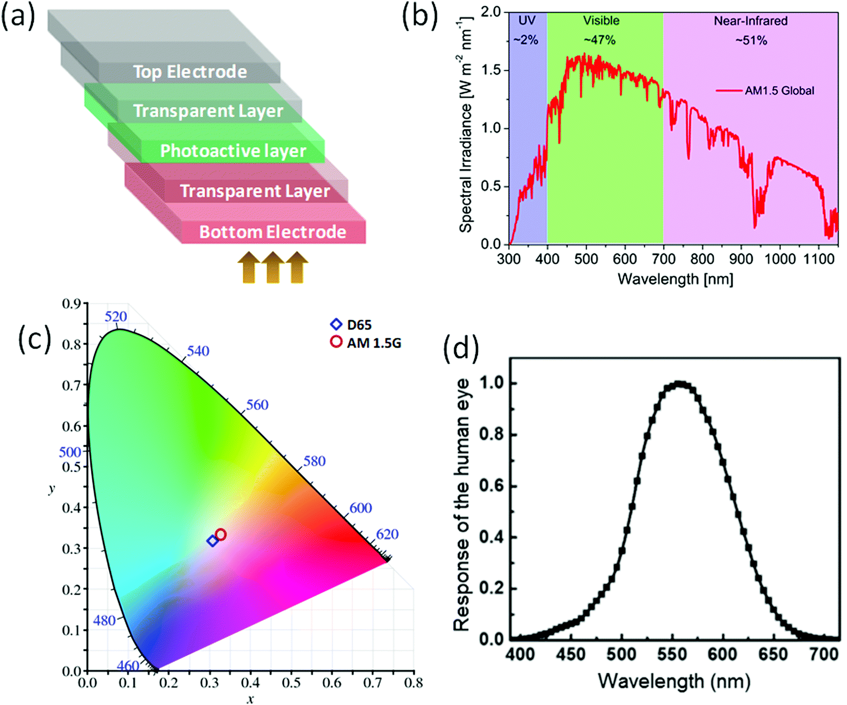 | ||
| Fig. 2 (a) Schematic diagram of the semitransparent organic solar cell, (b) solar emission spectrum and the energy fraction in the UV, visible and infrared regions, (c) corresponding color coordinates of semitransparent binary and ternary devices under AM 1.5G illumination on the Commission Internationale de l’Eclairage (CIE) 1931 chromaticity diagram, and (d) photopic spectral response of the human eye.18 Copyright 2020, Elsevier Ltd. | ||
The objective parameter quantum utilization efficiency (QUE), defined as the sum of the external quantum efficiency (EQE) and the transmittance (QUE = EQE + T), is used to evaluate the photon utilization efficiency in ST-OSCs. Due to intrinsic losses of photons and charge carriers in ST-OSCs the QUE value should be <90% over the visible region. The light utilization efficiency (LUE) is defined as the product of the PCE and the AVT (LUE = PCE × AVT).6 The LUE is used to compare the performance metrics between technologies and theoretical limits of different ST-OSCs.6,51 The trade-off between the AVT and the PCE needs to be optimized to improve the overall LUE of ST-OSCs.
3. A brief description of semitransparent OSCs
The key requirements for ST-OSCs typically include a blend layer of photoactive p-type donor and n-type electron acceptor materials, sandwiched between a front transparent electrode and a transparent reflective counter electrode. The anode and cathode interfacial buffer layers are placed between the active layer and electrodes to enhance the charge collection and charge-transport properties.15,16 Generally, ST-OSCs differ from common OSCs only with respect to the bottom transparent electrode. The prerequisites for bottom transparent electrodes are their (i) low cost, (ii) high transparency in the visible-light range and high reflectance in the near-infrared light range, and (iii) low sheet resistance/high conductivity. For a flexible ST-OSC the electrode should be highly resistive to cracks and bending.Organic semiconducting materials have a high molar absorption coefficient and a lower carrier mobility, so the thickness of the active layer is usually kept below 200 nm, which is sufficient for strong light absorption to bring the optical semitransparency.3,9,16,18,25 The absorption spectra of the organic materials can also be tuned from the visible to the NIR region via bandgap engineering to obtain color-tunable ST-OSCs. In the following sections we will discuss the current developments in ST-OSCs with respect to the interfacial carrier-transport layers, photoactive materials and top and bottom electrodes. The solar cell parameters are presented in Table 1.
| Photoactive layer | Cathode | Anode | V OC [V] | J SC [mA cm−2] | FF | PCE [%] | AVT [%] | Ref. |
|---|---|---|---|---|---|---|---|---|
| Conductive metal oxide | ||||||||
| P3HT:PC61BM | ITO/TiO2 | MoO3/ITO | 0.53 | 6.3 | 0.57 | 1.9 | 80 (>650 nm) | 83 |
| PCDTBT:PC71BM | TiOx/Al/ZAO | ITO/PEDOT:PSS | 0.84 | 9.2 | 0.48 | 3.9 | 34 | 87 |
| P3HT:PC61BM | ZAO | ITO/PEDOT:PSS | 0.45 | 8.24 | 0.28 | 1.0 | 77 @ 700 nm | 86 |
| P3HT:PC61BM | ZAO(400 nm)/LiF/Al | ITO/PEDOT:PSS | 0.59 | 9.35 | 0.61 | 3.4 | 60.7 @ 700 nm | 86 |
| P3HT:PC61BM | ITO/nc-TiO2 | V2O5/Ag/V2O5 | 0.58 | 4.83 | 0.61 | 1.7 | — | 92 |
| PBDB-T:ITIC | ITO/ZnO | MoO3/Ag/WO3 | 0.88 | 13.8 | 0.60 | 7.4 | 25.2 | 94 |
| Conductive PEDOT:PSS polymer | ||||||||
| P3HT:PC61BM | ITO/ZnO/PEIE | PEDOT:PSS | 0.57 | 6.91 | 0.51 | 2.04 | 51.2 | 107 |
| PTB7:PC71BM | ITO/PEIE | PEDOT:PSS–PDMS | 0.72 | 11.97 | 0.44 | 3.75 | 35 | 109 |
| PTB7-Th:IDTBR | ITO/ZnO | PEDOT:PSS/IL | 0.98 | 11.35 | 0.57 | 6.32 | 35.4 | 110 |
| P3HT:IDT-2BR | PES/PH1000/PEIE | PEDOT:PSS PH1000-T | 0.84 | 5.93 | 0.58 | 2.88 | 50 | 112 |
| PBDB-T-2F:Y6 | PDINO/Al | PET/D-PEDOT:PSS/PEDOT:PSS (4083) | 0.80 | 19.28 | 0.68 | 10.53 | 21 | 111 |
| P3TI:PC71BM | ITO/Rinsed PFPA-1 | PEDOT:PSS PH1000 | 0.69 | 8.08 | 0.60 | 3.35 | ∼50.0 | 105 |
| TQ1:PC71BM | ITO/Rinsed PFPA-1 | PEDOT:PSS PH1000 | 0.77 | 5.46 | 0.62 | 2.61 | ∼50.0 | 105 |
| Metal nanowires | ||||||||
| P3HT:PC61BM | ITO/AZO | PEDOT:PSS/Ag NWs | 0.56 | 5.83 | 0.65 | 2.13 | — | 114 |
| PBDTT-FDPP-C12:PC61BM | TiO2/Ag NW | ITO/PEDOT:PSS | 0.76 | 9.1 | 0.61 | 4.3 | 62.0 | 121 |
| PBDTT-SeDPP:PC61BM | TiO2/Ag NW | ITO/PEDOT:PSS | 0.73 | 10.9 | 0.58 | 4.6 | 63.0 | 121 |
| P3HT:Si-PCPDTBT:PC61BM | Ag NWs/AZO | PEDOT:PSS/Ag NWs | 0.57 | 6.4 | 0.60 | 2.2 | 33 | 122 |
| P3HT:PC61BM | ZnO/TiOx/Ag NWs | PEDOT:PSS/GO/PEDOT:PSS | 0.58 | 8.2 | 0.49 | 2.3 | 55 @ 650 nm | 124 |
| PBDTT-DPP:PC61BM | TiO2/Ag NWs | ITO/PEDOT:PSS | 0.77 | 9.3 | 0.56 | 4.0 | 66 @ 550 nm | 125 |
| PBTZT-stat-BDTT-8:PC61BM | PET:PEDOT:PSS:AgNW/ZnO | PEDOT:PSS:AgNW | 0.73 | 8.9 | 0.58 | 3.8 | 25 | 129 |
| P3HT:PC61BM derivative | Polyacrylate/Cu NWs/PEDOT:PSS (PH1000)/Y-TiO2 | PEDOT:PSS(4083)/CuNWs/polyimide/PDMS | 0.62 | 7.08 | 0.45 | 1.97 | 42 | 130 |
| PBDB-TF:Y7 | ANZnO/Al (15 nm). | ITO/PEDOT:PSS | 0.83 | 23.6 | 0.70 | 13.76 | 19.09 | 132 |
| Ultrathin metal | ||||||||
| PBDTTT-C-T:PC71BM | ITO/ZnO/C60-SAM | MoO3/Ag | 0.76 | 13.01 | 0.63 | 6.22 | 21.3 | 46 |
| PTB7-Th:IEICO-4F | PNDIT-F3N-Br/Au (1 nm)/Ag (12 nm) | ITO/PEDOT:PSS | 0.67 | 18.9 | 0.62 | 8.1 | 21.1 | 137 |
| PTB7-Th/IEICO-4F | PNDIT-F3N-Br/Au (1 nm)/Ag (12 nm) | ITO/PEDOT:PSS | 0.67 | 19.6 | 0.65 | 8.5 | 21.5 | 137 |
| PTB7-Th:PC71BM | PF3N-2TNDI(ETL)/Ag | ITO/PEDOT:PSS | 0.76 | 11.62 | 0.68 | 6.05 | 30.35 | 142 |
| PTB7-Th:PC71BM | PF3N-2TNDI(ETL)/Ag | ITO/PEDOT:PSS | 0.77 | 12.66 | 0.70 | 6.78 | 20.71 | 142 |
| P3HT:PC71BM | LiF/Al/Ag (20 nm) | ITO/PEDOT:PSS | 0.61 | 8.4 | 0.54 | 2.7 | 11 | 143 |
| PCDTBT:PC71BM | LiF/Al/Ag (20 nm) | ITO/PEDOT:PSS | 0.90 | 6.6 | 0.51 | 3.0 | 16 | 143 |
| PBDTTT-CT:PC71BM | LiF/Al/Ag (20 nm) | ITO/PEDOT:PSS | 0.82 | 13.8 | 0.46 | 5.2 | 14 | 143 |
| PBDTTT-EFT:PC71BM | LiF/Al/Ag (20 nm) | ITO/PEDOT:PSS | 0.84 | 11.0 | 0.61 | 5.6 | 10 | 143 |
| PBDB-T-2F:PC71BM | ITO/PFN | MoO3/Au | 0.96 | 9.4 | 0.63 | 5.7 | 67.0 | 144 |
| PBDB-T-2F:Y6 | ITO/SnO2 | MoO3/Ag (15 nm) | 0.83 | 21.56 | 0.72 | 12.88 | 25.6 | 76 |
| PBDB-T-2F:IT-4F | ITO/SnO2 | MoO3/Ag (15 nm) | 0.79 | 19.74 | 0.72 | 11.2 | 26.2 | 76 |
| PBDB-TF:Y6 | ITO/Al(acac)3 | MoO3/Ag | 0.82 | 20.73 | 0.73 | 12.41 | 25.33 | 77 |
| PBDB-TF:Y6 | ITO/ZnO | MoO3/Ag | 0.82 | 19.80 | 0.74 | 12.01 | 23.65 | 77 |
| PCPDTFBT:PC71BM | ITO/ZnO | PEDOT:PSS/Ag | 0.74 | 11.4 | 0.59 | 5.0 | 47.0 | 145 |
| PTB7-Th:PC71BM | ITO/ZnO | MoO3/Ag | 0.81 | 14.59 | 0.72 | 8.52 | 26.2 | 146 |
| PBDTTT-E-T:IEICO | PFN-2TNDI-Br/Ag (14 nm) | ITO/PEDOT:PSS | 0.81 | 14.4 | 0.66 | 7.9 | 23.8 | 147 |
| PTB7-Th:ITVfIC | PDINO/Ag (15 nm) | ITO/PEDOT:PSS | 0.74 | 17.54 | 0.63 | 8.21 | 26.4 | 148 |
| PBDB-TF:ID-4Cl | PDINO/Au (15 nm) | ITO/PEDOT:PSS | 0.75 | 13.77 | 0.68 | 6.99 | 43.7 | 149 |
| PBN-S:IT-4F | ZnO/Au (1 nm)/Ag (20 nm) | ITO/PEDOT:PSS | 0.88 | 15.48 | 0.65 | 9.83 | 32.0 | 150 |
| PTB7-Th:IEICO-4F | PDIN/Au (1 nm)/Ag (11 nm) | ITO/PEDOT:PSS | 0.71 | 18.81 | 0.68 | 9.06 | 27.1 | 151 |
| D18:N3 | PDIN/Au (1 nm)/Ag (10 nm) | ITO/PEDOT:PSS | 0.83 | 20.9 | 0.74 | 12.91 | 22.49 | 152 |
| PTB7-Th:IEICO-4F | PET/Ag mesh/PH 1000/ZnO | MoO3/Au (1 nm)/Ag (15 nm) | 0.71 | 20.27 | 0.67 | 10.03 | 34.2 | 153 |
| PTB7-Th:FOIC | ITO/ZnO | MoO3/Au (1 nm)/Ag (15 nm) | 0.74 | 20.0 | 0.70 | 10.3 | 37.4 | 154 |
| PTB7-Th:FOIC | ITO/PFN | MoO3/Ag (15 nm)/WO3/Pt | 0.74 | 20.3 | 0.67 | 10.23 | 25.4 | 155 |
| PBDB-TF:Y6 | ITO/PEDOT:PSS | PDIN/Au (1 nm)/Ag (10 nm) | 0.85 | 20.35 | 0.71 | 12.37 | 18.6 | 156 |
| PTB7-Th:ATT-2 | ZrAcac/Ag | ITO/PEDOT:PSS | 0.71 | 18.53 | 0.59 | 7.74 | 37.0 | 157 |
| PTB7-Th:IEICS-4F | ITO/ZnO/PFN | MoO3/Au (1 nm)/Ag (20 nm) | 0.74 | 22.5 | 0.66 | 11.1 | 28.6 | 158 |
| PTB7-Th:BT-CIC | ITO/ZnO | MoO3/Ag (20 nm) | 0.68 | 18.0 | 0.68 | 8.2 | 26.0 | 159 |
| PTB7-Th:BT-CIC | ITO/ZnO | MoO3/Ag (15 nm) | 0.68 | 17.0 | 0.67 | 7.7 | 33.0 | 159 |
| J52:IEICO-4Cl | PFN-Br/Au(15 nm) | ITO/PEDOT:PSS | 0.73 | 19.6 | 0.59 | 6.37 | 35.1 | 160 |
| PBDB-T:IEICO-4Cl | PFN-Br/Au (15 nm) | ITO/PEDOT:PSS | 0.73 | 19.6 | 0.59 | 6.24 | 35.7 | 160 |
| PTB7-Th:IEICO-4Cl | PFN-Br/Au (15 nm) | ITO/PEDOT:PSS | 0.73 | 19.6 | 0.59 | 6.97 | 33.5 | 160 |
| PTB7-Th:IEICO-4Cl | PFN-Br/Au (30 nm) | ITO/PEDOT:PSS | 0.73 | 19.6 | 0.59 | 8.38 | 25.6 | 160 |
| PTB7-Th:IHIC | ITO/ZnO | MoO3/Au (1 nm)/Ag (15 nm) | 0.75 | 19.01 | 0.68 | 9.77 | 36.0 | 161 |
| PTB7-Th:FNIC2 | ITO/ZnO | MoO3/Ag (20 nm) | 0.73 | 21.87 | 0.73 | 11.6 | 13.6 | 162 |
| PTB7 -Th:FNIC2 | ITO/ZnO | MoO3/Ag (14 nm) | 0.72 | 19.1 | 0.69 | 9.51 | 20.3 | 162 |
| PTB7-Th:IUIC | ITO/ZnO | MoO3/Au (1 nm)/Ag (15 nm) | 0.79 | 18.31 | 70.3 | 10.2 | 31.0 | 163 |
| PTB7-Th:IT-4F | ITO/ZnO | MoO3/Au (1 nm)/Ag (15 nm) | 0.68 | 13.2 | 0.72 | 6.42 | 28.0 | 163 |
| PFBDB-T:C8-ITIC | ITO/ZnO | MoO3/Ag/MoO3 (10/15/40 nm) | 0.92 | 15.5 | 0.70 | 9.8 | 22.0 | 164 |
| PBDB-T:Y14 | ITO/SnO2 | MoO3/Ag (15 nm) | 0.79 | 22.5 | 0.72 | 12.67 | 23.7 | 165 |
| PTB7-Th:BDTThIT-4F | PDIN/Au (1 nm)/Ag (10 nm) | ITO/PEDOT:PSS | 0.73 | 15.13 | 0.68 | 7.53 | 24.2 | 190 |
| PTB7-Th:IEICO-4F | PDIN/Au (1 nm)/Ag (10 nm) | ITO/PEDOT:PSS | 0.72 | 19.17 | 0.60 | 8.35 | 25.3 | 190 |
| Carbon nanotube (CNT) | ||||||||
| /P3HT:PC61BM | ITO/ZnO | CNT | 0.57 | 10.5 | 0.40 | 2.5 | 80 @ 670 nm | 168 |
| C60/ZnPc:C60 | ITO/n-C60 | p-BF-DPB/CNT | 0.57 | 4.5 | 0.58 | 1.5 | — | 169 |
| PTB7:PC61BM | ITO/ZnO | CNT without dopant | 0.66 | 6.5 | 0.40 | 1.8 | 80 @ 400 nm | 170 |
| PTB7:PC61BM | ITO/ZnO | MoOx-Doped CNT | 0.62 | 8.8 | 0.56 | 3.1 | 170 | |
| PTB7:PC61BM | ITO/ZnO | HNO3-Doped CNT | 0.69 | 9.5 | 0.56 | 3.7 | 170 | |
| Graphene | ||||||||
| P3HT:PC61BM | ITO/ZnO | GO/graphene (10 layers) | 0.54 | 10.5 | 0.44 | 2.5 | 70 @ 650 nm | 175 |
| P3HT:PC61BM | ITO/ZnO | PEDOT:PSS/Au-doped graphene | 0.59 | 10.58 | 0.43 | 2.7 | — | 176 |
| PTB7:PC71BM | ZnO-NP/PEDOT:PSS/graphene | Graphene/PEDOT:PSS | 0.67 | 12.1 | 0.41 | 3.4 | 40 | 177 |
| Photoactive layer | Cathode | Anode | V OC [V] | J SC [mA cm−2] | FF | PCE [%] | AVT [%] | Ref. |
|---|---|---|---|---|---|---|---|---|
| Ternary devices | ||||||||
| PTB7-Th:PBT1-S:PC71BM/ | ZrAcac/Ag | ITO/PEDOT:PSS | 0.83 | 15.6 | 0.71 | 9.2 | 20.0 | 188 |
| PTB7-Th1:COi8DFIC:IEICO-4F | ITO/ZnO | MoO3/Ag (10 nm) | 0.71 | 14.94 | 0.64 | 6.78 | 24.18 | 189 |
| PTB7-Th1:COi8DFIC:IEICO-4F | ITO/ZnO | MoO3/Ag (15 nm) | 0.71 | 17.35 | 0.67 | 8.23 | 20.78 | 189 |
| PTB7-Th1:COi8DFIC:IEICO-4F | ITO/ZnO | MoO3/Ag (20 nm) | 0.71 | 19.52 | 0.67 | 9.37 | 17.23 | 189 |
| PTB7-Th:BDTThIT-4F:IEICO-4F | PDIN/Au/Ag | ITO/PEDOT:PSS | 0.73 | 19.21 | 0.67 | 9.40 | 24.6 | 190 |
| D18-Cl:Y6-1O:Y6 | PDIN/Au/Ag | ITO/PEDOT:PSS | 0.88 | 19.56 | 0.75 | 13.02 | 20.2 | 191 |
| J52:IEICO-4F:PC71BM | PFN-Br/Ag | ITO/PEDOT:PSS | 0.69 | 19.04 | 0.67 | 8.83 | 15.8 | 192 |
| PCDTBT:PC71BM:ITIC | ITO/ZnO | MoO3/Ag/MoO3 | 0.89 | 8.65 | 0.52 | 4.02 | 39 | 193 |
| PBDB-TF:Y6:DTNIF | PDIN/Ag | ITO/PEDOT:PSS | 0.86 | 23.61 | 0.72 | 14.50 | 19.78 | 195 |
| PBDB-TF:Y6:DTNIF | PDIN/Ag | ITO/PEDOT:PSS | 0.85 | 22.71 | 0.70 | 13.49 | 22.58 | 195 |
| PBDB-TF:Y6:DTNIF | PDIN/Ag | ITO/PEDOT:PSS | 0.84 | 20.56 | 69.93 | 12.14 | 25.89 | 195 |
| Tandem devices | ||||||||
| TQ1:PC71BM (front) | ITO/Rinsed PFPA-1 | PEDOT:PSS PH1000 | 1.46 | 6.03 | 0.64 | 5.63 | ∼25.0 | 105 |
| P3TI:PC71BM (rear) | ||||||||
| PIDT-phanQ:PC61BM (front) | ITO/ZnO/C60-SAM | (ICL: m-PEDOT:PSS/PEDOT:PSS PH1000/ZnO) MoO3/Ag | 1.63 | 5.23 | 0.69 | 7.4 | 40.0 | 197 |
| PIDT-phanQ:PC71BM (rear) | ||||||||
| P3TEA:FTTB-PDI4 (front) | ITO/ZnO | (ICL: PEDOT:PSS/ZnO) MoO3/Au | 1.73 | 9.62 | 0.63 | 10.5 | 20.0 | 198 |
| PTB7-Th:IEICS-4F (rear) | ||||||||
| PBDTT-FDPP-C12:PC61BM (front) | TiO2/Ag NW | (ICL: PFN/TiO2/PEDOT:PSS) ITO/PEDOT:PSS | 1.47 | 8.4 | 0.59 | 7.3 | 30.0 | 121 |
| PBDTT-SeDPP:PC71BM (Rear) | ||||||||
| PSEHTT:IC60BA (front) | TiO2/Ag NWs | (ICL: ZnO/PEDOT:PSS) graphene mesh/PEDOT:PSS | 1.62 | 7.62 | 0.64 | 8.02 | 44.9 | 199 |
| PBDTT-DPP:PC71BM (rear) | ||||||||
| Photoactive layer | Cathode | Anode | V OC [V] | J SC [mA cm−2] | FF | PCE [%] | AVT [%] | Ref. |
|---|---|---|---|---|---|---|---|---|
| PCDTBT:PC71BM | ITO/TiO2 | WO3/Ag/1DPC | 0.87 | 9.67 | 0.63 | 5.31 | 25.1 | 50 |
| PTB7:PC71BM | BCP/Ag/LiF/[MoO3/LiF] | ITO/PEDOT:PSS | 0.73 | 10.9 | 0.70 | 5.6 | 30.0 | 201 |
| P3HT:PC61BM | ITO/ZnO | MoOx/(Au/Ag)/DM-6 | 0.56 | 10.4 | 0.55 | 3.2 | 19.0 | 202 |
| PTB7:PC71BM | ITO/ZnO | MoOx/(Au/Ag)/DM-6 | 0.73 | 12.8 | 0.68 | 6.4 | 16.9 | 202 |
| PTB7-Th:PC71BM | ITO/ZnO | MoOx/(Au/Ag)/DM-6 | 0.79 | 13.1 | 0.68 | 7.0 | 12.2 | 202 |
| PTB7-Th:PC71BM | 1DPC/Au/ZnO | MoOx/Ag/MoOx/LiF | 0.73 | 10.7 | 0.68 | 5.3 | 21.4 | 203 |
| PTB7-Th:IEICO-4F | PFN-Br/Ag/1DPC | ITO/PEDOT:PSS | 0.72 | 21.9 | 0.69 | 10.83 | 29.5 | 204 |
| P3HT:ICBA | ITO/PEI | WO3/Ag/[WO3/LiF]pairs | 0.87 | 8.79 | 0.67 | 5.12 | 24.4 | 205 |
| PTB7-Th:PC71BM | ITO/PFN | MoO3/Ag/WO3(x)/[WO3/LiF]5 | 0.79 | 17.15 | 0.69 | 9.36 | 14.31 | 206 |
| J71:IHIC | PDINO/Au/Ag/3-DMs | ITO/PEDOT:PSS | 0.81 | 18.54 | 0.57 | 8.48 | 21.5 | 207 |
| PTB7-Th:IHIC | PDINO/Au/Ag/3-DMs | ITO/PEDOT:PSS | 0.75 | 17.7 | 0.65 | 8.48 | 20.5 | 207 |
| J71:PTB7-Th:IHIC | PDINO/Au/Ag/3-DMs | ITO/PEDOT:PSS | 0.76 | 21.08 | 0.58 | 9.37 | 21.4 | 207 |
3.1. Carrier transport layers
Carrier-transport layers (CTLs), which are placed between the transparent electrode and photoactive layer, play an essential role in the performance of ST-OSCs. A proper selection of CTLs leads to an enhanced PCE and the long-term stability of the device. In OSCs the hole-transport layer (HTL) can be separated into two categories: inorganic HTLs and organic HTLs.52 Although OSCs with inorganic HTLs can achieve a satisfactory PCE, the processing technique of high-temperature vacuum evaporation makes them unsuitable for large-scale commercial roll-to-roll production. Inorganic p-type transition metal oxides or metal sulphides, such as MoO3, V2O5,53 NiO,54 WO3,55 and MoS2,56 are the most commonly used HTLs in OSCs. By contrast, organic HTLs show numerous advantages, including low cost, large area roll-to-roll processibility, non-toxicity, and a wide range of fabrication flexibility. Organic HTLs include conductive polymers such as PEDOT:PSS,57 conductive polyelectrolytes,58 and graphene oxide.59 In inverted OSCs, ZnO,60 AZO (aluminum-doped ZnO), ZTO (zinc tin oxide),61,62 TiO2,63 and Cs2CO364 have been used as electron-transport layers (ETLs). The lifetime and stability of ST-OSCs have been significantly improved using a ZnMgO-modified cathode layer and thin MoO3/Ag as the anode.65 Cao and co-workers used ZnO/C60-SAM as the ETL and the MoO3/Au/Ag transparent anode to improve the AVT and LUE.66Generally, in opaque OSCs, the CTL is only used for the charge-transport process; however, besides charge transport the optical properties of CTLs are considered crucial in ST-OSCs. In ST-OSCs, ZnO and PEDOT:PSS are widely used as CTLs because of their excellent charge-carrier properties.67–69 However, their optical properties are not sufficiently ideal for ST-OSCs.48,70 About 30–40-nm-thick CTL films are deposited to obtain pinhole-free films, which eventually reduced their transmittance. The ZnO ETL has an AVT of around only 80–85%, which limits the transmittance of ST-OSCs. Recently, Kadam et al. introduced polyethyleneimine ethoxylated (PEIE)-doped ZnO as the ETL in flexible OSCs. The doping of PEIE causes a reduction of the work function of ZnO and passivates the interface, which results in an improved OSC performance.71 Although the PEDOT:PSS layer has a relatively high transmittance, it has a low environmental stability and shows low CRI values due to its intrinsic absorption. Further modification has been done to improve the stability and adhesive properties of PEDOT:PSS.72 Ozcan et al. found that the GO-doped PEDOT:PSS HTL enhances the PCE of the device by about 2.2%.73 Recently, Han et al. reported a hybrid HTL (h-HTL) incorporating WO3 and MoO3 in an NFA-based ST-OSC.74 The energy levels of the h-HTL can be easily controlled due to the high bond energies and electronegativities of the W and Mo atoms, resulting in strong conductivity and good film-forming capabilities. The ST-OSC module with an active area of 30 cm2 fabricated via printing process using the h-HTL exhibited a PCE of 7.2% and an AVT of 22.3%. More recently, Chaudhary et al. used TiO2 as the ETL in place of ZnO and suggested that the TiO2 ETL possess better operational stability for BIPV devices.75
Bai et al. employed chemically precipitated SnO2 colloidal particles as the ETL in ST-OSCs.76 They found that SnO2 CTLs exhibited excellent transparency with a high reflective index. The deep blue colored ST-OSCs fabricated using a blend of PBDB-TF:Y6 bulk heterojunction (BHJ) layer and SnO2 as the ETL and MoO3 as the HTL achieved a high PCE of 12.88%, an AVT of 25.6%, and a CRI value of 97.6. The PBDB-TF:ITIC-4F-based ST-OSC achieved a PCE of 11.2%, an AVT of 26.22% and a CRI value of 97.5. The same group further achieved a PCE of 12.41%, an AVT of 25.33%, and a CRI value of 94.6 using aluminum(III) acetylacetonate (Al(acac)3) as the CTL, in an ITO/Al(acac)3/PBDB-TF:Y6/MoO3/Ag device.77 Al(acac)3 showed an excellent transmittance up to 95% in the visible and near-infrared regions with a film thickness of 10 nm. By comparison, the AVT of the ST-OSC with a ZnO interlayer was 23.65% and the PCE was 12.01%. These encouraging findings suggest that the proper choice of CTL layers will significantly improve the efficiency of ST-OSCs. Some modification in CTLs is still needed to improve their optical properties for commercial applications. The utilization of CTLs (both HTLs and ETLs) in ST-OSCs is discussed in the following section along with the photoactive and electrode materials.
3.2. Photoactive layer engineering for ST-OSCs
The active layer, which consists of donor and acceptor units, plays a crucial role in ST-OSCs. These materials can be small molecules, conjugated polymers, or a combination of both. A list of polymer donors used in ST-OSCs is presented in Fig. 3. In the solar emission spectrum, the NIR region accounts for about 51% of the solar photon flux, 47% in the visible region and 2% in the UV region. Therefore, an ideal active layer should have a high transparency in the visible range with a strong light absorption in the UV and NIR regions for efficient ST-OSCs. The photoactive material must be chosen with the absorption peak located in the NIR or IR region to simultaneously improve the PCE and visible transparency.6 The choice of active layer materials also influences the apparent color of ST-OSCs. | ||
| Fig. 3 Chemical structures of polymer donors for ST-OSCs. | ||
Initially, the efficiency of ST-OSCs was very low (PCE < 3%) because of the use of a wide band gap (Eg > 1.9 eV) organic polymer donor and fullerene acceptor (FA) as the active layer materials, which can only harvest the photons of the UV-visible region. Therefore, a trade-off between the PCE and visible transparency arises.48 According to the Shockley–Queisser model, to obtain semitransparency the estimated band gap ranges from 1.36 eV to 1.12 eV (910–1100 nm). The low bandgap polymers in combination with fullerene acceptors reached PCEs of 3–7%. Later in 2017, fullerene-free acceptors emerged as NIR-absorbing molecules to improve the PCEs of ST-OSCs (Fig. 4). The device performance improved from ∼5% to 13% with AVT values ranging from 9 to 25%. Recently, Kini et al. reported the development of a photo-absorbing material for multifunctional ST-OSCs.78 Herein, we discuss the recent transformation from fullerene-based acceptors to NIR-absorbing FFAs to develop high-performance ST-OSCs with simultaneous color tunability and transparency.
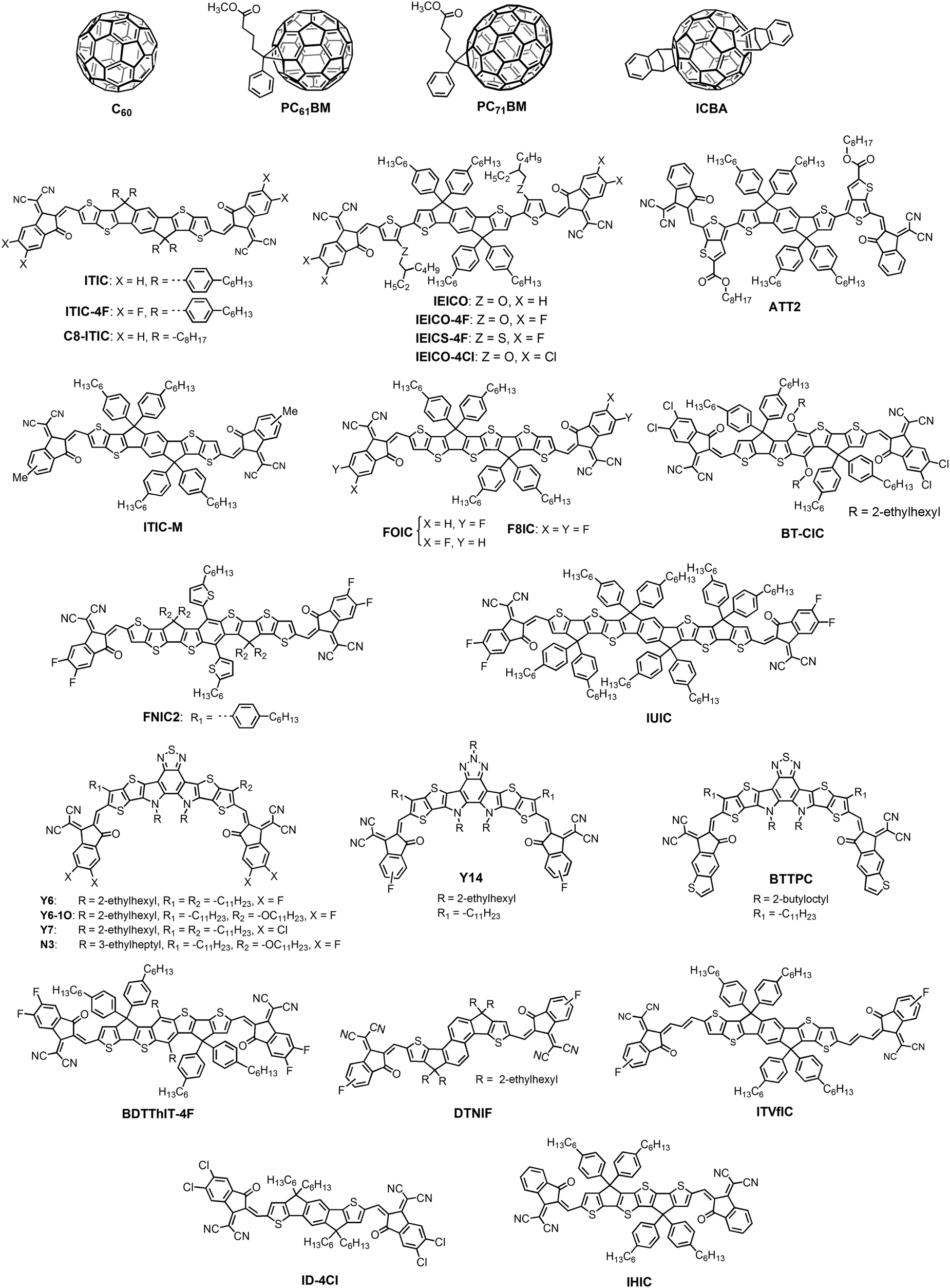 | ||
| Fig. 4 Chemical structures of fullerene and fullerene-free acceptors used in ST-OSCs. | ||
3.3. Semitransparent top electrode
In conventional OSCs, usually non-transparent highly reflective Al, Ag, Au or Pt are used as the metal electrode. Therefore, the electrode is one of the vital components in ST-OSCs. It should be transparent to obtain efficient ST-OSCs with a high average visible transmittance (AVT) with neutral color perception. The top electrodes generally transmit the light and transport charge carriers to or from the photoactive layers and supply the electric field. It is a most critical task to find a suitable transparent top electrode for ST-OSCs because it requires high transparency, high conductivity, and an appropriate work function. Many studies have been performed to develop transparent electrodes based on conducting polymers, metal oxides, graphene, carbon nanotubes (CNTs), ultrathin metal film, and metal nanowires (NWs) for ST-OSCs.79 | ||
| Fig. 5 (a) Schematic representation of the lamination process for device fabrication, (b) ST device, and (c) transmission curve and solar spectrum of the device.84 Copyright 2008, John Wiley Publishers. | ||
Aluminum (Al)-doped ZnO (AZO) was also used as the top transparent electrode for ST-OSCs.85 The use of AZO as the top electrode required sputtering, and therefore, a protecting layer is used underneath the AZO layer. Hanisch et al. obtained a PCE of 1% using a sputtered AZO film (400 nm) as the ST top electrode, showing transmittance values of 13.0% and 77% at 500 nm and 700 nm, respectively.86 Further optimization of the device by insertion of a layer of LiF/Al before the AZO electrode improved the PCE to 3.4% and with transmittance values of 60.7% and 9.3% at 700 nm and 500 nm, respectively. The LiF/Al layer simultaneously reduces the work function and protects the device from sputtering. Bauer et al. fabricated ST-OSCs with the ITO/PEDOT:PSS/PCDTBT:PC71BM/TiO2/Al/AZO structure, which gave a PCE of 3.9% with an AVT of 34%. The thin 4 nm Al layer prevents cracks forming due to direct contact of the AZO layer with TiO2. The TiO2 was used as the ETL and as a protective coating for the BHJ.87
In 2009, Chen et al. developed a ST-OSC using dielectric/metal/dielectric or DMD (MoO3/Ag/MoO3) as a transparent anode. The inner ultrathin layer of MoO3 (1 nm) works as a buffer layer to improve hole collection, while the outer layer of MoO3 served as a light-coupling layer to enhance the optical transmittance of the device and reduce the series resistance (Rs). The ITO/nc-TiO2/P3HT:PC71BM/MoO3/Ag/MoO3-based device exhibited a PCE of 1.40%.88 They further investigated the dependence of the device performance on the thickness of the outer MoO3 layer. Wilken et al. used ultrathin Au instead of Ag embedded between the two evaporated MoO3 layers as the anode and an Al-doped ZnO cathode to prepare ITO-free devices using a P3HT:PC61BM absorber, which showed a PCE of 2% and with 60% optical transmission.89 When MoOx/Ag/MoOx was incorporated as the transparent electrode in the PPT-PC61BM-based ST-OSC that used ZnO as the ETL, the device generated a maximum PCE of 4.1% with a good average light transmission of ∼60% over the 400–600 nm range.90 A PCE of 5.0% was achieved with 200-nm-thick PTB7:PC71BM and a 40 nm outer MoO3 layer in the MoO3/Ag/MoO3 electrode with an AVT of 18.3%.91 Other conducting oxides, like V2O5/Ag/V2O592 and zinc tin oxide (ZTO)/Ag/ZTO,93 were also used as top transparent electrodes, generating PCEs of 1.7% and 2.6%, respectively, with a transmittance of the electrodes of >80% from 400 to 750 nm.
Upama et al. reported a ST-OSC with an improved PCE of 7.4% (AVT = 25.2%) using the PBDB-T donor and the NIR-absorbing ITIC molecule.94 The top transparent electrode used was MoO3/Ag/MoO3. The authors showed the influence of the active-layer thickness on the device performance, and the device with a 100-nm-thick layer showed the best performance. The lowering of the thickness improved the AVT but significantly lowered the PCE due to a lack of active materials for light absorption.
Recently, Liu et al. introduced bifacial ST-OSCs with tellurium oxide (TeO2) on the top of an ultrathin Ag electrode as the optical coupling layer. The incorporation of TeO2 requires only one additional evaporation step and provides better CRI, AVT and LUE values. With the optimized thickness of the Ag/TeO2 (11/40 nm) electrode, the ST-OSCs with the structure of ITO/PEDOT:PSS/PBDB-TF:Y6:PC71BM/PDIN/Ag/TeO2 exhibit a PCE of 10.14% from the ITO side and 9.18% from the Ag side. The ST-OSCs had a high AVT of 27.83%, a high bifaciality factor of 90.53%, an improved LUE of 2.82%, and a CRI of 88.28. The device performance was also improved by applying a TeO2 capping layer in PTB7-Th:IEICO-4F-based ST-OSCs, indicating that the Ag/TeO2 back electrode shows great potential for upgrading bifacial ST-OSCs for future applications.95
Tang et al. applied two polymers based on pyrazine and isoindigo (P3TI and TQ1, respectively) as donors and PC71BM as an acceptor in combination with an amphiphilic conjugated polymer (PFPA-1)-modified ITO cathode and PEDOT:PSS PH1000 as the hole-collecting anode.105 The P3TI:PC71BM- and TQ1:PC71BM-based ST-OSCs achieved PCEs of 3.35 and 2.61%, respectively, with a visible transparency of ∼50%.
Colsmann and co-workers prepared an inverted ST-OSC using a modified PEDOT:PSS bilayer top electrode. The top PEDOT:PSS layer was blended with a red-absorbing cyanine dye which reduces the work function of the PEDOT:PSS electrode. The ITO/ZnO/PCDTBT:PC71BM/MoO3/PEDOT:PSS/PEDOT:PSS-dye device displayed a PCE of 1.9% with a high transmittance of ∼40% in the visible range.106
In 2019, Lee et al. reported solution-processed ST-OSCs fabricated using a PEDOT:PSS-based transparent top electrode, which showed a different average transmittance when the concentration of the active layer (P3HT and PC61BM) was varied from 1.5 to 3.1 wt% using an inverted device structure of ITO/ZnO/PEIE/P3HT:PC61BM/PEDOT:PSS. The highest PCE of 2% and transmittance of 51.2% were obtained with the concentration of 2.3 wt%.107 Several studies have been carried out to enhance the conductivity of PEDOT:PSS for ST-OSCs.100 In 2020, Kim et al. reported a highly conductive PEDOT:PSS polymer prepared from the mixture of PH 1000, AI 4083, and ethylene glycol as the additive solvent. The modified PEDOT:PSS can be used as both a HTL and an anode for all-solution-processed inverted ST-OSCs.108 The ST-OSC fabricated using modified PEDOT:PSS gave a PCE of 2.04% and a transmittance of >85%.
The realization of highly conductive stretchable PEDOT:PSS films is a big challenge due to strong acid treatments involved and their poor intrinsic stretchability. Using a unique dipping-embedded transfer printing process, Fan et al. developed a highly conductive stretchable PEDOT:PSS electrode with a novel dipping-embedded transfer printing technique using mild acids.103,109 The modified PEDOT:PSS, via treatment with 40 wt% CH4SO3, and a low viscous mild acid, on a quartz substrate, improved the conductivity (3470 S cm−1), transparency and mechanical stability of the electrode. The OSC with a device structure of PDMS/PEDOT:PSS–FTEs/PEDOT:PSS (4083)/PBDTT-S-TT:PC71BM/Ca/Al gave a PCE of 5.38%, a higher value than that of H2SO4-treated FETs (4.8%). The modified PEDOT:PSS film showed a high transmittance of over 90% from 380 to 800 nm.103 The transfer process of PEDOT:PSS using PDMS was carried out by dipping the PEDOT:PSS surface into PDMS liquid, followed by the penetration and solidification of the PDMS, which was then peel off quickly due to the strong interfacial adhesion between both materials (Fig. 6).109 The modified PDMS–PEDOT:PSS composite flexible film showed a high electrical conductivity of 2890 S cm−1. ST-OSCs prepared with ITO-coated glass substrates/polyethyleneimine (PEIE)/PTB7:PC71BM/PEDOT:PSS-PDMS showed high transparency of ∼35% in the visible region with a neutral color and PCEs of 3.75% and 3.46% when illuminated from the PDMS and ITO sides, respectively. The device performance was higher than the reference device with DMSO-doped PEDOT:PSS-PDMS (PCE = 2.86%, AVT = 31.1%).
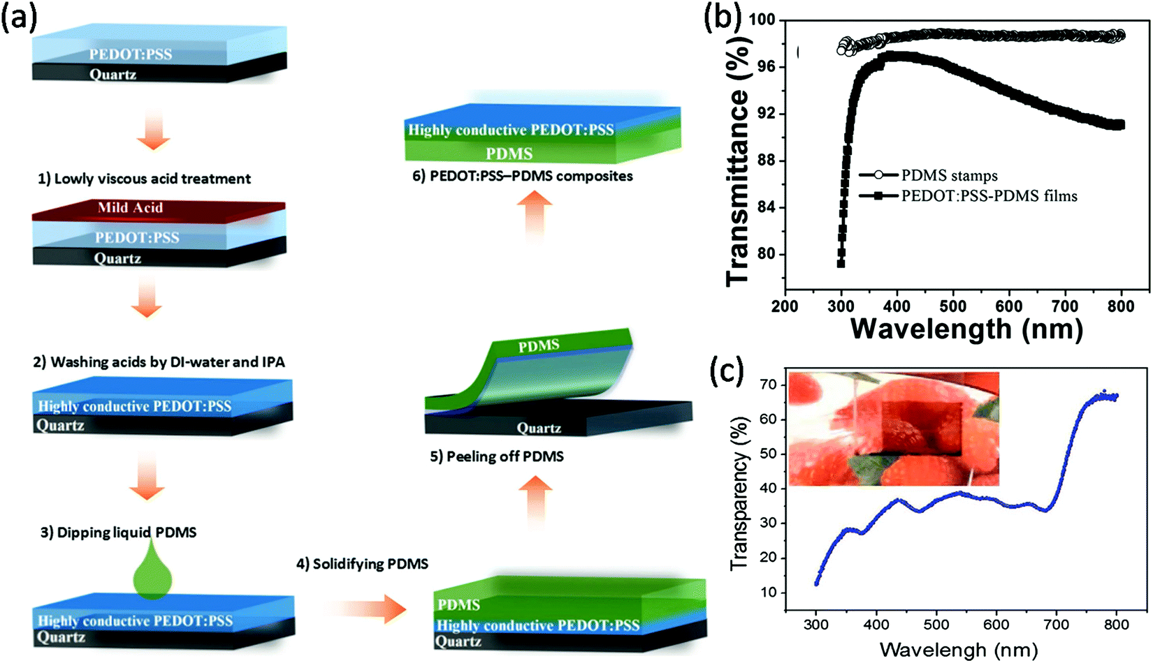 | ||
| Fig. 6 (a) Dipping-embedded transfer printing process, (b) transmittance spectra of the PEDOT:PSS–PDMS film, and (c) transmittance spectrum of the device with a photograph of the active ST-OSC (inset).109 Copyright 2017, John Wiley publishers. | ||
Lee and co-workers have shown two different printing techniques using a PEDOT:PSS/ionic liquid (IL) top electrode. First, they observed an increase in conductivity when the IL was mixed with PEDOT:PSS, but the underneath photoactive layer was oxidized during the ion exchange between PSS and the IL. Therefore, the group developed the sequential printing of PEDOT:PSS and the IL to prevent chemical doping of the photoactive layer by newly generated ion pairs due to retarded ion exchange (Fig. 7). The ST-OSC (ITO/ZnO NP/PTB7-Th:EH-IDTBR/PEDOT:PSS/IL) with sequential printing achieved a PCE of 6.32% and an AVT of 35.4% at an active layer thickness of 120 nm.110 A further increase in the thickness resulted in a reduction in both the AVT and PCE. The use of low bandgap materials resulted in a high visible transmittance for the 420–550 nm region.
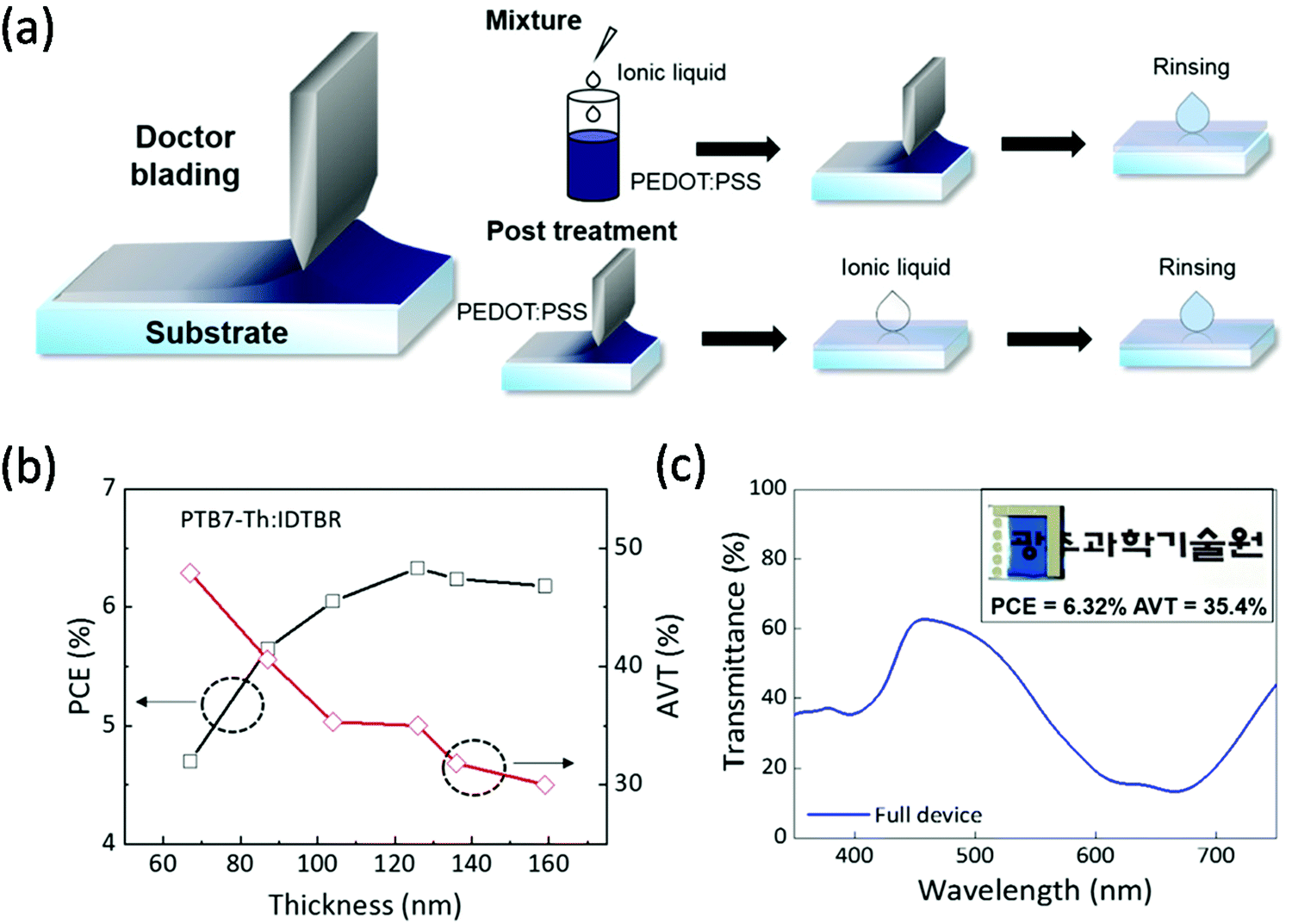 | ||
| Fig. 7 (a) Schematic representation of procedures used to manufacture PEDOT:PSS/IL composite electrodes; (top) a mixed solution of PEDOT:PSS and IL is printed and (bottom) PEDOT:PSS and IL are printed sequentially. (b) Effect of the photoactive layer's thickness on the device PCE and AVT. (c) Transmission spectrum of the device. The inset image shows an actual ST-OSC device with a PEDOT:PSS/IL top electrode.110 Copyright 2020, ACS. | ||
In 2020, Song et al. prepared a flexible electrode by doping a PEDOT:PSS aqueous solution with xylitol (a polyhydroxy compound) followed by surface treatment of the film with methanesulfonic acid (MSA). The doping of PEDOT:PSS with the polyhydroxy compound (xylitol) improved the phase separation with a fiber-like interconnected network due to H-bonding interactions between the xylitol and PSS, which was further improved via the treatment with MSA. The doping enhanced the adhesion ability of PEDOT on the PET substrate. The ST-OSC with the PET/D-PEDOT:PSS/PEDOT:PSS/PBDB-TF:Y6/PDINO/Ag (15 nm) structure achieved a PCE of 10.53% and an AVT of 21%.111 The flexible device also sustained about 1000 bending and folding cycles, still retaining 80% of the device PCE.
Wang et al. reported the first all-plastic flexible ST-OSCs with a P3HT:IDT-2BR-based non-fullerene photoactive layer.112 The PEDOT:PSS modified by a layer of polyethyleneimine (PEIE) was used as the bottom electrode, and the top electrode was prepared through film transfer of PEDOT:PSS via a lamination process using a PDMS substrate. The NF ST-OSC exhibited an AVT of 50% and a PCE of 2.88% with an enhanced bending stability. The results demonstrated the possibilities of conducting polymer semitransparent top electrodes for future applications in ST-OSCs.
Krantz et al. reported a PCE of 2% for P3HT:PC61BM-based inverted solar cells using spray-coated Ag NW layers as transparent top electrodes.114 ST-OSCs fabricated using PEDOT:PSS/Ag NW composite films formed on glass and a flexible PET substrate and with a P3HT:PC61BM active layer exhibited PCEs of up to ∼4.2% and ∼3.8%, respectively.120 Because of the composite film's lower sheet resistance, the device generated a higher fill factor on a flexible substrate. Yang and co-workers achieved decent PCE values of 4.3 and 4.6% in single-junction devices using PBDTT-FDPP-C12:PC61BM and PBDTT-SeDPP:PC61BM blends, respectively, using a TiO2/Ag NW top electrode, showing a high AVT of ∼62%.121 Guo et al. used Ag NW as both the top and bottom electrodes in Si-PCPDTBT:P3HT:PC61BM-based ternary devices, achieving a PCE of 2.2% and a FF of 0.63 with an AVT of 33%.122 The PCE and AVT were further improved to 2.9% and 41%, respectively, with pDPP5T-2:PC61BM in a fully solution-processed device structure of Ag NW/PEDOT:PSS/photoactive layer/ZnO/Ag NW (Fig. 8a and b).123 The thin layer of ZnO was introduced to improve the energy-level alignment and the formation of ohmic contacts between the active layer/ZnO and ZnO/Ag NWs. Yim et al. used solution-processed Ag NW and doped PEDOT:PSS as the cathode and anode, respectively, in P3HT:PC61BM-based devices and achieved a PCE of ∼2.3% with a visible transparency of ∼55% beyond 650 nm (Fig. 8c and d).124 TiO2/ZnO and AI4083/GO were used as the cathode and anode buffer layers, respectively.
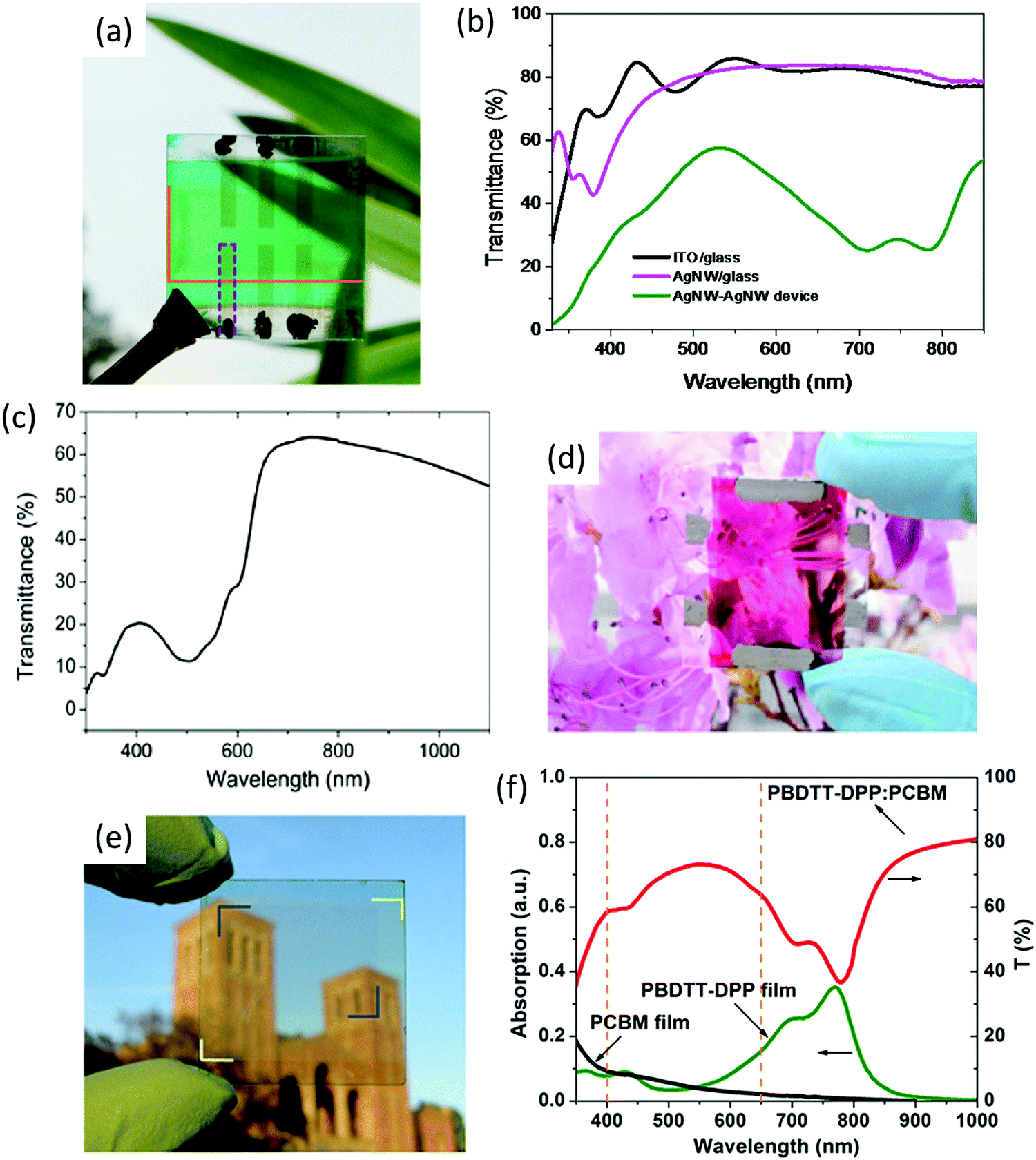 | ||
| Fig. 8 (a) Photograph and (b) transmittance spectra of the semitransparent AgNW–AgNW device,123 (c) optical transmittance spectrum of the device, and (d) photograph of a typical P3HT:PC61BM ST-OSC with AgNW- and PH1000-based electrodes.124 Copyright, 2014, ACS. (e) Photograph of a fully transparent organic solar cell in which the yellow and blue brackets indicate the top AgNW-based composite electrode and the bottom ITO electrode, respectively, and (f) absorption spectra of the pristine donor–acceptor materials and transmittance spectrum of the blend.125 Copyright, 2012, ACS. | ||
Kang et al. developed a fully spray-coated ST-OSC with Ag NWs as the top electrode and P3HT:PC61BM as the active layer, exhibiting a transmittance of ∼70% beyond 650 nm with a PCE comparable to a conventional metal electrode.115 Chen et al. demonstrated the use of a Ag NW-based composite transparent electrode formed via the spin-coating of a 10 wt% ITO nanoparticle dispersion onto the Ag NW matrix as a conducting filler in a ST-OSC.125 The photoactive layer was covered with a TiO2 layer over which the Ag NW dispersed in isopropanol was spray coated. The adhesion of the Ag NW network was improved by applying a dilute solution of sol–gel TiO2 in ethanol. The ITO/PEDOT:PSS/PBDTT-DPP:PC61BM/Ag NWs device gave a PCE of 4% and with a high AVT of 61% from 400 to 650 nm (Fig. 8e and f).
Min et al. prepared small-molecule ST-OSCs by inserting ZnO and the perylene diimide derivative (PDINO) as a cathode interfacial layer between the active layer and the top Ag NW-based transparent electrode.126 The ZnO/PDINO layer, apart from serving as a buffer layer, is also acting as a protective film for the active layer. Because of the variable absorptions of the active layers, various colorful ST devices can be prepared. The ZnO/PDINO/Ag NW electrode showed a transmittance of about 80% from 350 to 800 nm, which is similar to a pristine Ag NW or ITO electrode. The transmittance spectra of the devices with different active layers are between 30 and 55% (Fig. 9). The best device with the ITO/PEDOT:PSS/BHJ/ZnO/PDINO/Ag NW structure using BDTT-S-TR:PC71BM gave a PCE of 3.62% and an AVT of 32% at 435 nm. By contrast, other active layers demonstrated higher AVTs but with lower PCEs between 2.2 and 2.5%.
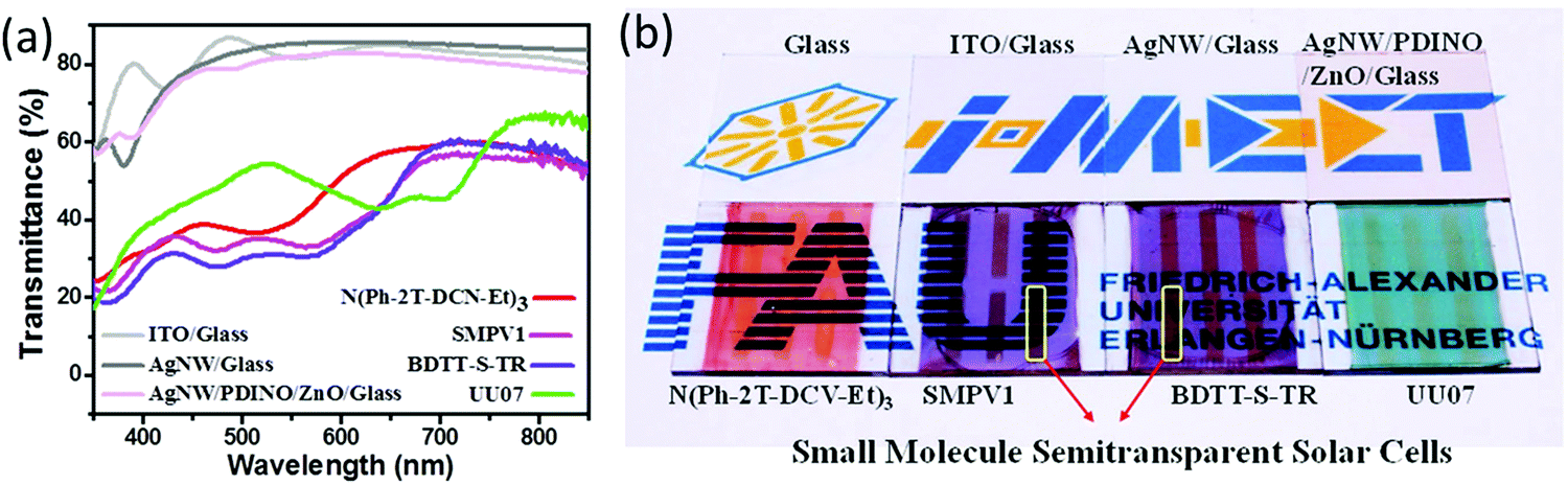 | ||
| Fig. 9 (a) Transmission spectra of the ITO, the pristine Ag NW film and the ZnO/PDINO/Ag NW stack along with the ST-OSCs based on small molecules, and (b) photograph of the ST devices showing the variable color transparency that is suitable for colorful power-generating windows.126 Copyright, 2016, John Wiley publishers. | ||
In 2016, the Colsmann group fabricated a large-area flexible ST-OSC with the PET/Ag mesh/PEDOT:PSS/ZnO/PffBT4T-2OD:PC61BM:PC71BM/PEDOT:PSS:Ag NWs structure using doctor-blade coating. They developed a transparent top electrode by intermixing PEDOT:PSS with Ag NWs. The PEDOT:PSS provides a homogeneous matrix for distribution of the Ag NWs. The SEM cross-section image showed the layer stacking of the device components with a homogeneous distribution of Ag NWs. The 1 cm2 large-area device realized a PCE of 5.9% with an AVT of 6% and a peak transmittance of 13% at 515 nm (Fig. 10).127
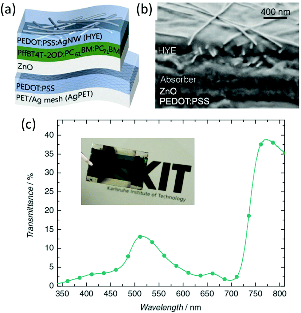 | ||
| Fig. 10 (a) Schematic of device architecture, and (b) cross-sectional SEM image of a typical all-doctor-bladed ST-OSC on Ag/PET with contrast enhancement. (c) Transmittance spectrum of a typical photoactive device. The inset shows a photograph of a specific doctor-blade-coated ST-OSC (>1 cm2).127 Copyright, 2016, John Wiley publishers. | ||
ITO NPs have a high carrier density, which can cause parasitic absorption in Ag NW-based transparent electrodes. To overcome this issue, Beiley et al. proposed replacing the ITO NPs with ZnO NPs. The composite top electrode of Ag NW–ZnO NPs has a low sheet resistance of 14 Ω sq−1, which is essential for large-scale manufacturing. The composite electrode showed an AVT of over 90%. The ST-OSCs with an active layer of PBDTTPD:PC71BM exhibited a PCE of 4–5%, which has an average above bandgap transmission of 34% and a sub-bandgap transmission of 81%.128 Koppitz et al. effectively used PEDOT:PSS–Ag NW hybrid electrodes as both top and bottom electrodes and prepared all-solution-processed ST-OSCs. The Ag NW-embedded PEDOT:PSS hybrid electrode was compressed via hot pressing after deposition to avoid any of the nanowires sticking out. The ST-OSC with a device structure of PET:PEDOT:PSS:Ag NW/ZnO/PBTZT-stat-BDTT-8:PC61BM/PEDOT:PSS:Ag NW, prepared using doctor blading, gave a PCE of 3.8% with an AVT of 25%.129
Zhai et al. reported inverted ST-OSCs with an all-copper-nanowire (Cu NW) electrode with a low surface roughness and homogeneous conductivity.130 They used the ‘in situ polymerization method’ for decreasing the roughness of the Cu NW-based electrodes. The fabricated ST-OSCs with the device structure of polyacrylate/CuNWs/PEDOT:PSS (PH1000)/Y-TiO2/P3HT:PC61BM/PEDOT:PSS(4083)/Cu NWs/polyimide/polydimethylsiloxane (PDMS) showed an AVT of 42% with PCE values of 1.97% and 1.85% for illumination from the top and bottom sides, respectively. The Cu NW/PI top electrode was coated with a thin layer of PEDOT:PSS(4083), and D-sorbitol was added as the electronic glue for adhesion of PEDOT:PSS with the active layer.
Ma and co-workers inserted phosphomolybdic acid (PMA) and PEDOT:PSS composite materials between the active layer and the Ag NW top electrode to improve the active layer wettability. The composite layer also has good solvent resistance and improves the wetting behavior with the Ag NWs. The device ITO/ZnO/PTB7-Th:PC71BM/PMA:PEDOT:PSS/Ag NW gave a PCE of 5.01% with an AVT of 50.3% when illuminated through ITO, while the device with MoO3/Ag/MoO3 as the transparent electrode showed a comparable PCE (5.77%) but with a lower AVT (19.5%).131 Illumination through the bottom Ag NW electrode gave a higher performance compared with the MoO3/Ag/MoO3 electrode.
Li and co-workers introduced Ag NWs into a ZnO film to increase the conductivity and LUE of PBDB-TF:Y7-based ST-OSCs without affecting the AVT.132 The LUE was improved from 2.46 to 2.63% with a PCE of 13.76% and an AVT of 19.09%. The improvement was mainly due to the increase in JSC resulting from the high conductivity and surface plasmon resonance of the Ag NWs. This study demonstrates an efficient approach for fabricating ST-OSCs with a high LUE. Grossman and co-workers prepared a Ag NW-based anode encapsulated with graphene oxide to protect it from degradation and simultaneously increase the lifetime of inverted ST-OSCs.133
These metal NW transparent electrodes have a promising future for ST-OSCs. However, a judicious choice of solvent is necessary to prevent the solvent-induced corrosion of the metal NWs or conducting polymers. The solvent used for the preparation of the electrodes could harm the carrier-transport layer and the active layer beneath it. Future research will require careful solvent selection for solution-processed transparent electrodes.
ST-OSCs fabricated using a chloro-aluminum phthalocyanine (ClAlPc) or BODIPY derivative as the donor, and C60 as the acceptor in a bilayer structure achieved a high AVT of >55% and a PCE of approximately 2%.134,135 Bilayer OSCs are fabricated via the sequential deposition of donor and acceptor materials. Hany and co-workers used Ag/Alq3 cathodes to prepare ST-OSCs and achieved a PCE of 1% and an AVT of over 65% with a maximum of 78.8% at 568 nm using a near-IR-absorbing cyanine dye donor.136 The formation of a planar heterojunction results in insufficient donor–acceptor interfaces for exciton dissociation. So subsequently, the BHJ structure has often been used to fabricate most of the ST-OSCs. Though the BHJ structure is beneficial for obtaining high-performance ST-OSCs, it is also hard to optimize and control the phase separation in the BHJ active layer. The bulk morphology is rarely the thermodynamically stable situation at equilibrium. The bilayer structure may be able to prevent this unstable morphological problem, resulting in an improved device stability for ST-OSCs. Therefore, exploring the potential of the active layers in the bilayer structure would be fascinating.
Recently, Song et al. deposited a bilayer of the PTB7-Th/IEICO-4F-based active layer to fabricated ST-OSCs. They found that the bilayer deposition not only simplified the processing but also improved the PCE of the device compared with the BHJ-based device. They pointed out that the thickness of the IEICO-4F acceptor does not affect the visible transmittance while absorbing in the near-IR region for charge generation (Fig. 11). By optimizing the thickness of the acceptor and donor materials and using Au/Ag (1/12 nm) as the ultrathin transparent top electrode, the device exhibited a PCE of 8.5% with an AVT of 21%, which is better than the PCE of 8.1% (AVT = 21.1%) obtained for the BHJ structure.137
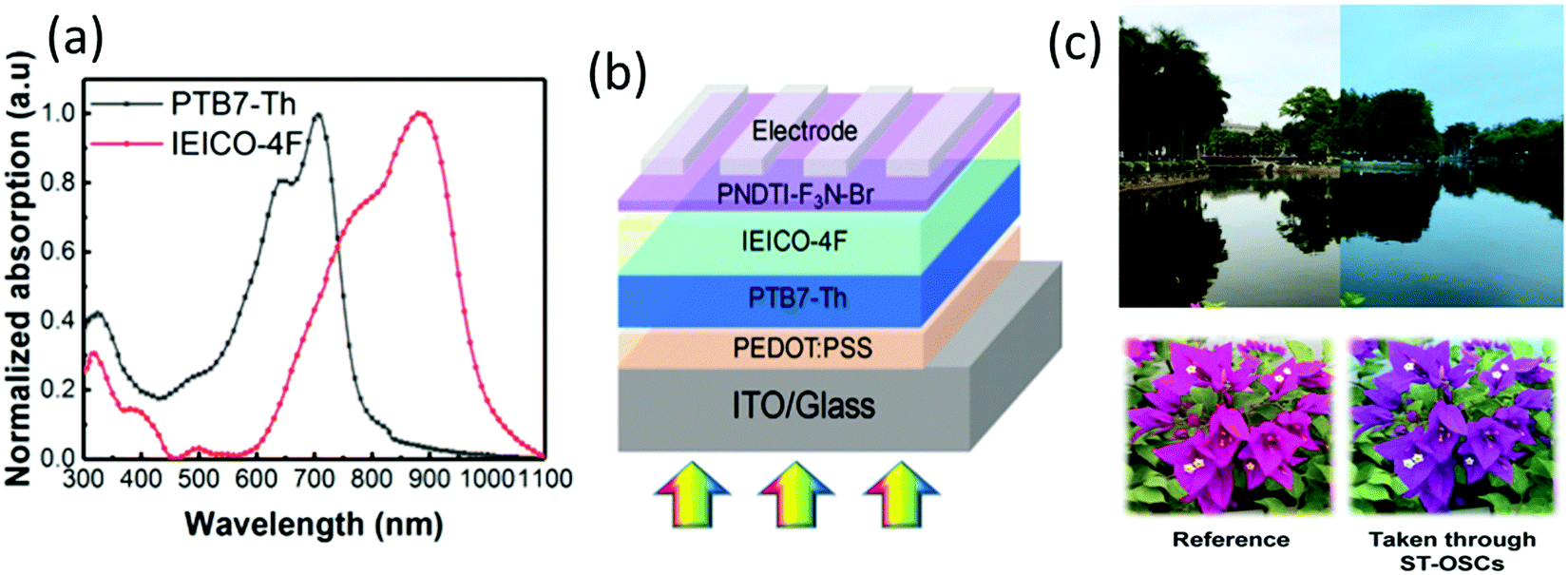 | ||
| Fig. 11 (a) Normalized absorption spectra of donor and acceptor units, (b) device structure of the bilayer ST-OSCs, and (c) digital photographs taken through the reference device and ST-OSCs devices.137 Copyright 2020, ACS. | ||
In 2006 Yang et al. used a thin Au (12 nm) layer as the top transparent electrode in inverted ST-OSCs.138 The BHJ device with the structure ITO/Cs2CO3/P3HT:PC61BM/V2O5/Au exhibited a PCE of 0.85% when illuminated through the ITO side and 0.52% by illuminating the Au electrode. The comparatively low PCE from the semitransparent Au electrode is due to the partial loss of photons via absorption and reflection.
UTMFs prepared via vapor deposition exhibited poor adherence to the underlying substrate because of their tendency to develop through the island-like Volmer–Weber nucleation pattern, leading to a rough surface morphology with a high electrical resistivity.139 Rough surfaces generally form plasmonic resonances with visible light, thus significantly reducing the film transparency. Therefore, to reduce the surface roughness and increase the visible transparency it is important to control the wetting behavior of the metal or to insert a dielectric layer by application of a thin (0.1–1 nm) nucleation layer of metal, which shifts the percolation threshold of the thinner film and lowers the electrical resistance.79,140 Apart from metals, solution-processed PEDOT:PSS has also been used as a viable nucleation layer. Nucleation layers can help the thermally formed ultrathin metal layer to percolate onto the underlying substrate, resulting in a better film quality.141
Schubert et al. demonstrated an efficient Ag top transparent electrode with a 1-nm-thick Au layer as the metal seed layer in a dielectric/metal/dielectric (DMD) multilayer structure. The Au/Ag bilayer is sandwiched between two MoO3 layers that serve as the dielectric to increase electrode transparency and to improve the device lifetime. They observed that the transmittance and conductance of the Ag films vary due to the significant variation of the substrate wetting conditions. The transparent electrode with ultrathin 1 nm Au and 7 nm Ag exhibited a maximum transmittance of 83% at 580 nm, which is even higher compared with ITO in this spectral range. The insertion of a 1 nm Au seed layer in the Ag layer decreased the sheet resistance (Rs) from 32 Ω sq−1 to 19 Ω sq−1. The device with F4ZnPc:C60 achieved PCEs of 4.6% and 4.7% when illuminated from the ITO and Au (1 nm)/Ag (7 nm) layer sides, respectively.140
Jen et al. reported a bilayer semitransparent hybrid electrode prepared via thin Ag metal deposition on an ultra-thin fullerene-containing surfactant as the cathode interfacial layer (CIL).19 The CIL adjusts the energy-level alignment at the metal/organic interface and efficiently enables electron extraction and photocurrent generation. The fabricated ST-OSCs using a thin layer of PIDT-PhanQ:PC71BM (50 nm) as the active layer and a hybrid transparent electrode containing 30 nm Ag exhibited a PCE of 5.1% with an AVT of ∼25% from 400 to 800 nm and have a good color perception that was close to white light (Fig. 12). The PCE improvement is related to an increase in the VOC and the FF.
 | ||
| Fig. 12 (a) Transmission spectra of the ST-OSCs with varying thickness of the Ag electrode in the visible range. (b) Top: representation of the color coordinates of ST-OSCs on the CIE 1931 xy chromaticity diagram upon illumination with AM1.5G; and bottom: the relevant expanded part of the color space of the CIE 1931 xy diagram. Inset (in between): two digital pictures taken through the ST-OSC that has a 20-nm-thick Ag layer.19 Copyright, 2012, John Wiley publishers. | ||
Recently, Shi et al. reported an ST-OSC with an ultra-thin Ag layer (7 nm) as the top transparent electrode and PF3N-2TNDI, a self-doped n-type polymer, as the ETL.142 The ST-OSC ITO/PEDOT:PSS/PTB7-Th:PC71BM/PF3N-2TNDI/Ag structure exhibited a PCE of 6% with an AVT of 30%. Moreover, the ST-OSC exhibited a CRI approaching 100% and CIE color coordinates of (0.326,0.328). Wong et al. prepared ST-OSCs using a bilayer of an ultrathin metal film (LiF/Al/Ag) as the top transparent electrode. Blade-coated ST-OSCs based on the PBDTTT-CT:PC71BM and PTB7-Th:PC71BM active layers with PEDOT:PSS as the HTL gave PCEs of 5.2 and 5.6%, respectively, with an AVT between 10 and 20% for the 400–800 nm region with good color perception and high CRI of ∼90, making them suitable for building-integrated photovoltaic window applications.143 Large-area devices with 10.8 cm2 gave a PCE of 3.8 and 5.3%, respectively, for ST-OSCs using the different active layers.
Jen and co-workers prepared an inverted ST-OSC using a low band-gap polymer PBDTTT-C-T as the donor and PC71BM as the acceptor (Fig. 13).46 The complementary absorpton of the donor and acceptor materials resulted in a neutral color appearance of the device over the visible spectral region. They further showed that the AVT could be tuned from 36% to 2% by increasing the thickness of the Ag electrode from 6 to 60 nm, with PCEs ranging from 4.25 to 7.56% and with a CRI value of about 97 using a device structure of ITO/ZnO/C60-SAM/PBDTTT-C-T:PC71BM/MoO3/Ag. Hou and co-workers prepared an inverted ST-OSC using the wide bandgap polymer donor PBDB-TF with a deep HOMO energy level (−5.45 eV) and the PC71BM acceptor, achieving a PCE of 5.7%, a VOC of 0.96 V, and an excellent average transmission of 67% in the visible region.144
 | ||
| Fig. 13 Transmission spectra of ST-OSCs obtained via optical modeling (closed symbols) and from the actual devices (open symbols); (b) photograph of a flower taken with a camera; and (c) photograph taken through the bare glass, the ITO and the ST-OSCs with the Ah electrode of different thicknesses.46 Copyright, Royal Society of Chemistry. | ||
Jen and co-workers reported the use of a fluoro-containing polymer donor PCPDTFBT which, with the PC71BM acceptor, gave a PCE of 5% and a high AVT of 47.3% using a 10 nm thin Ag on top of PEDOT:PSS as an anode. Increasing the Ag thickness to 15 nm dis not affect the PCE (5.1%); however, the AVT dramatically decreased to 39.4% for the 450–900 nm region.145 Cao's group achieved the highest PCE of 6.78% in a ST-OSC using the PTB7-Th:PC71BM active layer after interfacial modification with 5-nm-thick PF3N-2TNDI and a 20 nm Ag electrode.142
Dudem et al. created a subwavelength architecture using polydimethylsiloxane (SWA-PDMS) as an anti-reflective (AR) layer via the soft imprinting lithography technique to simultaneously improve the PCE, the transparency and the color perception.146 The PCE of the modified device with the AR layer was enhanced from 7.07% to 8.52%, with AVT increasing from 23.0% to 26.2%. The CRI value increased from 84% to 90% using the SWA-PDMS layer.
Cao and co-workers fabricated an ST-OSC using the PBDTTT-E-T:IEICO active layer, which showed a PCE of 7.9% and an AVT of 23.8%.147 The thickness-dependent study of the Ag electrode showed that with an increase in the Ag thickness from 10 to 20 nm the device PCE increased from 6.8 to 9.0% while the AVT decreased from 28 to 17%. They further revealed that at the same AVT of ∼20% the ST-OSC with a fullerene-free acceptor achieved a higher PCE of 8.4% compared with 6.2% for a fullerene-based device, which was mainly due to the contribution of absorption from the NIR region.
Huang et al. fabricated an ST-OSC using the PTB7-Th polymer donor and ITVfIC as the acceptor, achieving a PCE of 8.21% with an AVT of 26.4% between 370 and 740 nm without any additional treatment. The thin film of ITVfIC displayed an absorption peak at 772 nm with a bandgap of 1.37 eV, thus complementing the absorption of PTB7-Th (λmax = 690 nm).148 Li et al. prepared a ST-OSC with a PBDB-TF:ID-4Cl blend achieving a PCE of 6.99%, lower than the opaque device (10.2%), and an AVT of 43.7%.149 Wu et al. achieved a PCE of 9.83% with an AVT of 32% in a ST-OSC with a bluish color by employing a PBN-S:IT-4F blend and a 20-nm-thick Ag cathode. The polymer PBN-S displayed a strong absorption for the 500–700 nm region with a low-lying HOMO energy level (−5.48 eV), which is compatible with IT-4F. The opaque device with PBN-S:IT-4F gave a high PCE of 13.1% due to efficient charge separation and transport.150
Hu et al. reported a smart strategy of adjusting the D![[thin space (1/6-em)]](https://www.rsc.org/images/entities/char_2009.gif) :A weight ratio. Opaque and ST-OSCs were prepared by optimizing the doping ratios of PTB7-Th:IEICO-4F blends. The opaque OSCs maintained PCEs of over 11% by altering the PTB7-Th:IEICO-4F ratios from 1.4:1.5 to 0.8:1.5 (wt/wt), along with a red-shifted absorption edge of the active layers resulting from the molecular aggregation of IEICO-4F. The ST-OSCs were prepared with 1 nm Au/11 nm Ag replacing 100 nm Al as the electrode. The AVT of the ST-OSCs was increased from 23.7% to 27.1% by decreasing the PTB7-Th content in the active layers, along with a slight decrease in the PCE from 9.48% to 9.06%.151
:A weight ratio. Opaque and ST-OSCs were prepared by optimizing the doping ratios of PTB7-Th:IEICO-4F blends. The opaque OSCs maintained PCEs of over 11% by altering the PTB7-Th:IEICO-4F ratios from 1.4:1.5 to 0.8:1.5 (wt/wt), along with a red-shifted absorption edge of the active layers resulting from the molecular aggregation of IEICO-4F. The ST-OSCs were prepared with 1 nm Au/11 nm Ag replacing 100 nm Al as the electrode. The AVT of the ST-OSCs was increased from 23.7% to 27.1% by decreasing the PTB7-Th content in the active layers, along with a slight decrease in the PCE from 9.48% to 9.06%.151
In addition to decreasing the relative weight ratio of D:A, Xu et al. proposed an effective strategy of using the wide bandgap polymer donor D18, which has a small absorption full-width half-maximum (FWHM) of 118 nm, to enhance the AVT of ST-OSCs.152 The small FWHM of D18 can enable narrow photon harvesting in the visible-light range, which is promising for the preparation of high-efficiency ST-OSCs. Combining the strategy of decreasing the D:A weight ratio and optimizing the thickness of the semitransparent top electrode, a highest LUE of 2.90% with a PCE of 12.91% and an AVT of 22.49% was achieved in the D18:N3-based ST-OSCs.
Yang's group developed flexible ST-OSCs with good visible transparency, which used visible light for the growth of plants and NIR light for generation of the current. The devices, which used PTB7-Th as the donor and IEICO-4F, F8IC and FOIC acceptors, achieved high PCEs of 10.03%, 9.26% and 8.92%, respectively, with a AVT of ∼34% which is suitable for plant-growth applications.153 Zhan and co-workers synthesized a fused-ring octacyclic fullerene-free acceptor (FOIC), which exhibits an absorption maximum at 836 nm with an optical gap of 1.32 eV. The as-cast ST-OSC exhibited an excellent PCE of 10.3% and an AVT of 37.4% from 370 to 740 nm due to the strong absorption of the acceptor in the NIR region.154 The authors further prepared a ST-OSC with a PCE of 10.2% and an AVT of 25.4% for PTB7-Th:FOIC photoactive layer, which can be reversibly switched on and off by implementation of the gasochromic WO3/Pt back-reflector layer under hydrogen exposure. The device was also found to improve the AVT to 33.8% under the bleached state whilst still maintaining a PCE of 9.1%, suggesting a color-switchable ST-OSC.155 Hu et al. achieved a PCE of 12.37% and an 18.6% AVT using the PBDB-TF:Y6 photoactive layer.156 The transmittance was adjusted by manipulating the thickness of the Ag layer.
Zhu and co-workers developed an acceptor ATT-2, which shows a strong NIR absorption between 600 and 940 nm with an optical energy gap of 1.32 eV. A blend layer of PTB7-Th:ATT-2 achieved a PCE of 7.7% and a high transparency of 37% with good color-rendering properties (CRI = 94) and CIE color coordinates of (0.2805,0.3076).157 Chen et al. used the PTB7-Th donor and the low bandgap IEICS-4F acceptor (Eg = 1.3 eV) and achieved a PCE improvement from 9.4 to 11.1% with an AVT of 43.2 to 28.6%, respectively, by varying the thickness of the Ag electrode from 10 to 20 nm in the MoO3/Au/Ag electrode.158 The reduction of the Ag thickness enhanced the AVT but reduced the PCE value.
Li et al. used an inverted device ITO/ZnO/PTB7-Th:BT-CIC/MoO3/Ag, which exhibited a PCE of 7.1% with an AVT = 43%, when measured from the ITO side, and a CRI value of 91. It was shown that the increase in the Ag thickness reduced the visible transmittance (Fig. 14a); the ST-OSC with 10-nm-thick Ag is shown in Fig. 14b.159
 | ||
| Fig. 14 (a) Optical transmittance of ST-OSCs with varying thicknesses of the Ag electrode, and (b) photograph of the PTB7-Th:BT-CIC-based ST-OSC.159 (c) Transmittance spectra of ST-OSC devices with various donor materials, and (d) photograph of the ST-OSCs with an active donor layer of J52, PBDB-T, or PTB7-Th when using the IEICO-4Cl acceptor (from left to right).160 Copyright, 2017, John Wiley and Sons publishers. | ||
Hou and co-workers achieved variable-color ST-OSCs from purple, to blue to cyan when using J52, PBDB-T, and PTB7-Th as the donor and IEICO-4Cl the acceptor (PCE 6.2–6.97% and AVT of ∼35%) (Fig. 14c and d). The devices gave a PCE of around 4% when illuminated through the Au electrode.160 When PTB7-Th was blended with IHIC acceptor the best ST-OSC gave a PCE of 9.77% without sacrificing the AVT (36%) with a Au/Ag top electrode.161 A higher PCE of 11.6% could be observed with the PTB7-Th:FNIC2 blend but at the cost of the AVT (13.6%).162 When PTB7-Th was mixed with a complementary absorbing low bandgap acceptor IUIC the ST-OSC with the ITO/ZnO/PTB7-Th:IUIC/MoOx/Au(1 nm)/Ag structure displayed a PCE of 10.2% and an AVT of 31% with >40% from the 370–500 nm region.163
Moreover, Heeney and co-workers used a fullerene-free acceptor C8-ITIC and the PFBDB-T donor as the absorber layer in the ST-OSC prepared using a MoO3/Ag/MoO3 top electrode and an ITO/ZnO bottom electrode, providing an average PCE of 9.8% and an AVT of 22%, with CIE coordinates of (0.24,0.29).164 The thickness of the MoO3/Ag/MoO3 layer was optimized at 10/15/40 nm to give the best device performance. Luo et al. reported an efficient ST-OSC using the fused dithienothiophen[3,2-b]-pyrrolobenzotriazole-based fullerene-free acceptor Y14 absorbing from 300 to 1000 nm. The Y14-based inverted ST-OSC after additive and thermal-annealing treatment reached an excellent PCE of 12.67% whilst still maintaining a high AVT of 23.69% which is required for window applications.165 The opaque device gave a PCE of 14.92%.
3.3.5.1. Carbon nanotubes (CNTs). Carbon nanotubes (CNTs) are one of the allotropes of carbon, which offer excellent flexibility, high conductivity, carrier mobility, chemical and mechanical stability and visible transparency. These properties make CNTs a potential candidate for the top transparent electrode.166,167 The resistance of a CNT network depends on many factors like the length, diameter, purity, synthetic method, and metallic/semiconducting volume ratio and is governed by the contact resistance between the CNTs and their individual resistance. Besides, the surface roughness of CNT films can result in a considerable shunt resistance loss.
Xia et al. prepared CNT films via the chemical vapor deposition (CVD) method and used them as a transparent top electrode in ST-OSCs. The CNT films exhibit 80–95% transmittance for the 400–2500 nm wavelength range and a sheet resistance of 400–600 Ω cm−1. The ST-OSCs were prepared with the ITO/ZnO/P3HT:PC61BM/CNT structure and showed PCEs of up to 2.5% and an AVT of 60–80% from NIR to the IR region.168 Kim et al. used free-standing multi-wall carbon nanotube (f-CNT) sheets as the top electrode in ZnPc:C60-based ST-OSCs. The f-CNT electrode was deposited on top of the BHJ layer at room temperature using an orthogonal liquid solution-assisted self-laminating process. The ITO/n-C60/C60/ZnPc:C60/p-BF-DPB/f-CNT device generated PCEs of 1.3% or 1.0% when illuminated from the ITO or CNT sides, respectively. The CNT-based devices showed higher FF values and stability compared with devices using the Al (1 nm)/Ag (14 nm) semitransparent top electrode.169 Joen et al. developed an aerosol method to synthesize a transparent CNT electrode with strong interchain interactions. The CNT films were p-doped using HNO3via ‘sandwich transfer’, and thermally evaporated MoOxvia ‘bridge transfer’ and fabricated using a lamination process. The doped CNT-based devices using ZnO as the ETL and PTB7:PC71BM as the active layer generated PCEs of 3.7 and 3.1%, respectively, with a transmittance of 90% compared with 1.8% for the un-doped device. It was observed that the conductivity of the CNTs was increased with the doping process.170
3.3.5.2. Graphene-based electrode. Graphene is the thinnest 2-D carbon allotrope, comprising sp2 hybridized carbon. Graphene has all the properties for becoming a good semitransparent electrode for OSCs, such as high conductivity, high transparency (90% in NIR range), a high mechanical, chemical, and thermal stability, a low sheet resistance, and high carrier mobility. Graphene electrodes can be fabricated using various methods like chemical vapor deposition (CVD), chemical synthesis, unzipping of CNT mechanical exfoliation, and the reduction of graphene oxide (rGO).171–174 Lee et al. reported an inverted ST-OSC with a laminated graphene top electrode without damaging the underlying active layer. For the top electrode, graphene film was deposited on top of the ITO/ZnO/P3HT:PC61BM/GO device with thermal release tape followed by the removal of the tape during thermal annealing. The device achieved a maximum PCE of 2.5% with a high transparency beyond 700 nm (Fig. 15).175 The transmittance and sheet resistance of the graphene layer were found to be decreased by increasing the number of graphene layers.
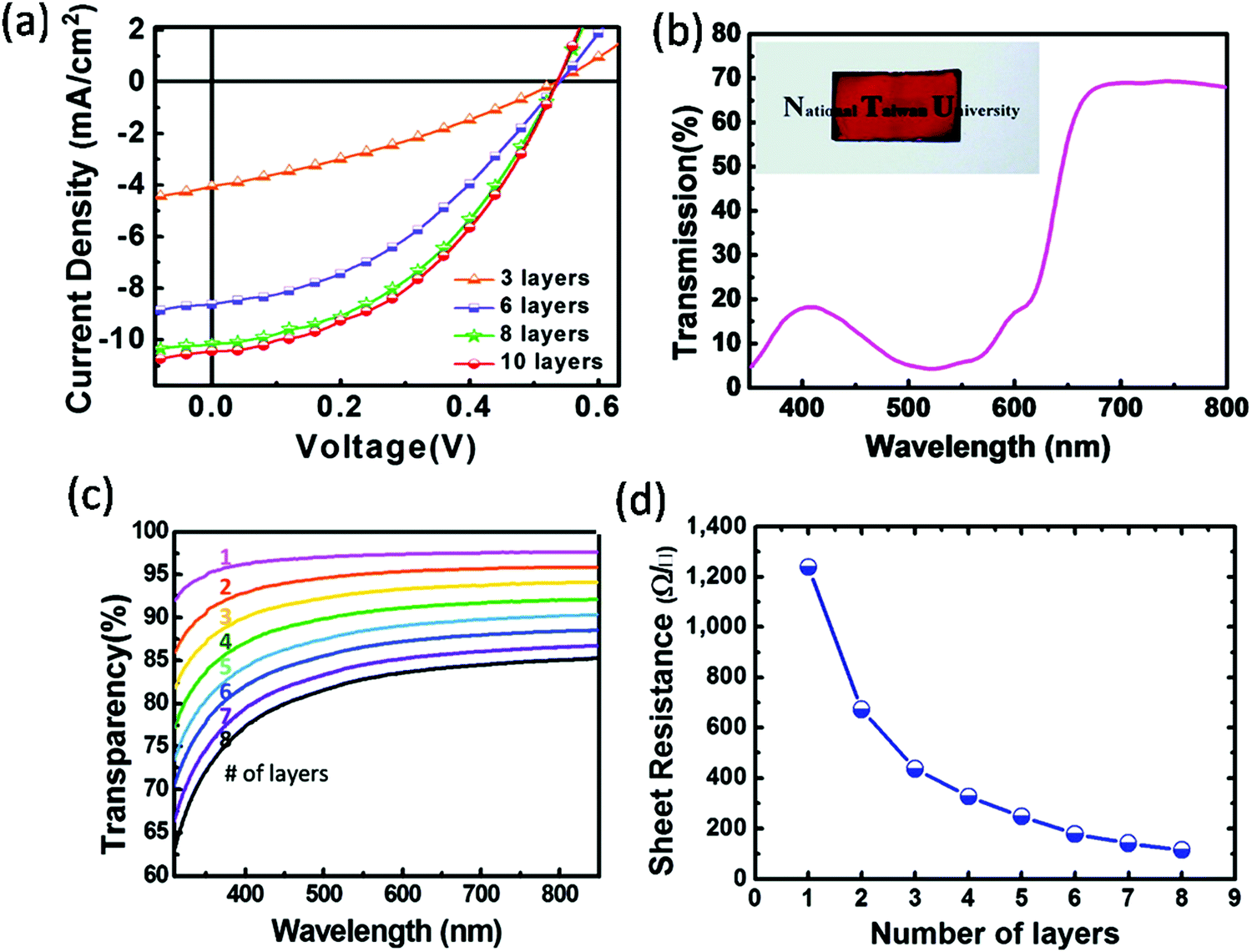 | ||
| Fig. 15 (a) Current–voltage characteristics of the ST-OSCs that consist of various top graphene layers with light shining from the ITO side; (b) transmittance spectrum with a picture of the semitransparent device in the inset; and (c) transparency and (d) sheet resistance of graphene film layers on a glass substrate.175 Copyright 2011, ACS. | ||
Yan et al. used highly doped single-layer graphene as the top electrode in an inverted ST-OSC with the P3HT:PC61BM active layer. The conductivity of graphene was found to be increased by doping with Au nanoparticles and PEDOT:PSS. The graphene film was p-doped by PEDOT:PSS due to the high work function of the latter, resulting in electron transfer from graphene to PEDOT:PSS. The optimized ITO/ZnO/P3HT:PC61BM/PEDOT:PSS/graphene devices using the doped single-layer graphene electrode resulted in the best PCE of 2.7% in a 20 mm2 active area.176 Liu et al. fabricated ST-OSCs using graphene as both the transparent cathode and anode. In this process, the graphene film was n-doped with ZnO NPs. The devices with the modified ZnO-NP/PEDOT:PSS/graphene cathode gave the best PCE of 5.78% compared with the device with only a ZnO NP (4.89%) buffer layer due to lowering of the sheet resistance and improved FF. For all graphene electrode-based devices, the graphene anode was laminated via a graphene/PMMA film staked on a thin PDMS substrate. The graphene/PMMA/PDMS film was p-doped with PEDOT:PSS, and D-sorbitol was used to improve the adhesion on the active layer during the lamination process (Fig. 16). The device with the graphene/PEDOT:PSS/PTB7:PC71BM/ZnO NP/PEDOT:PSS/graphene structure fabricated via a lamination process exhibited a PCE of up to 3.35% and an AVT of 40%.177 The measurement through the modified bottom cathode side showed a slightly lower performance than with illumination through the top anode side. The device showed excellent color neutrality (0.3098,0.3306) that was close to white light.
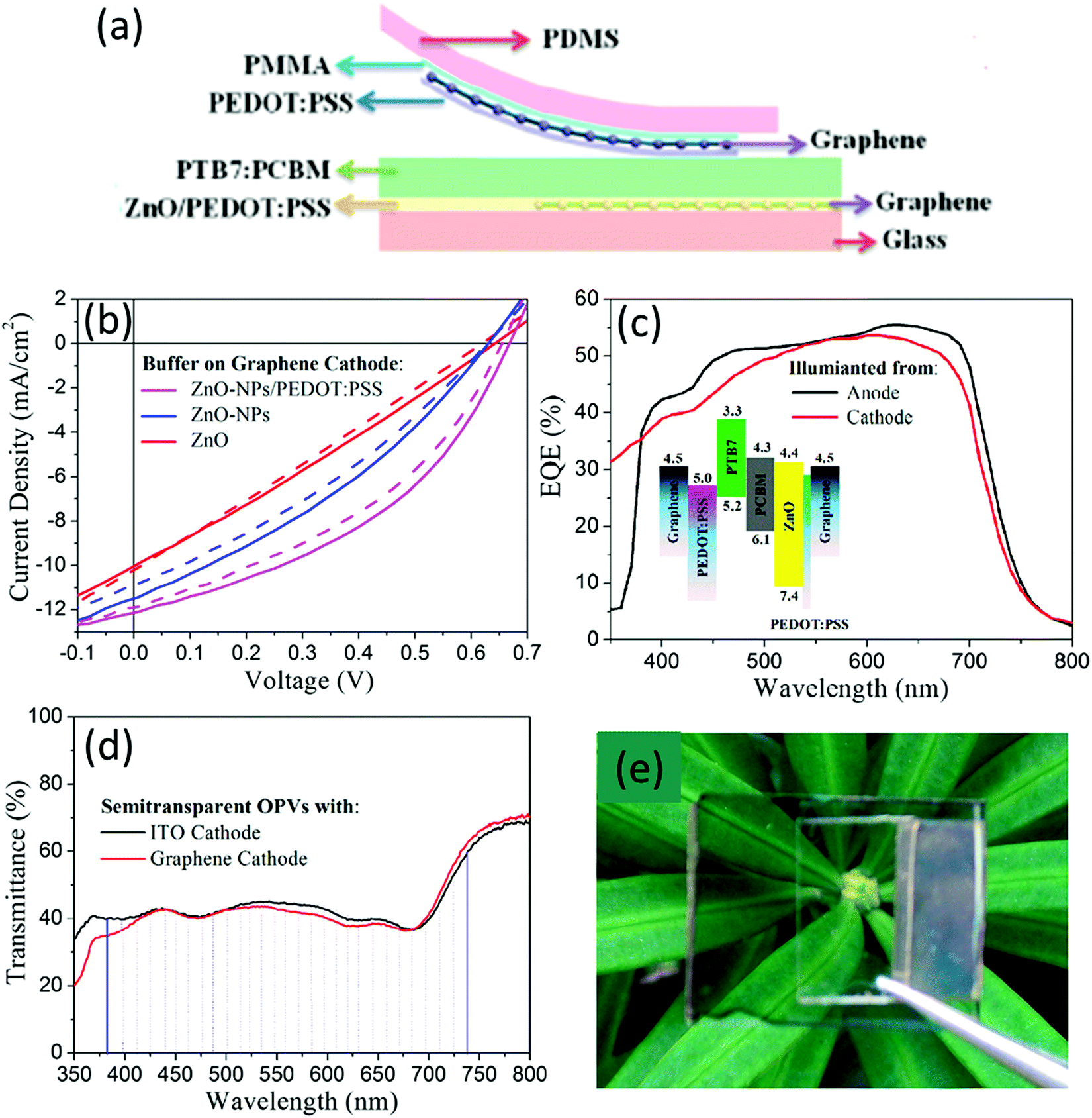 | ||
| Fig. 16 (a) Schematic representation of laminated all-graphene electrodes; (b) J–V characteristics of OSCs with all-graphene electrodes, where solid lines and dashed lines represent illumination from the anode side and the cathode side, respectively; (c) EQE spectra taken from each side of an ST-OSC with a graphene cathode modified with ZnO-NPs/PEDOT:PSS. Inset: the device's energy diagram; (d) transmittance spectra of two ST-OSCs with a graphene cathode and an ITO cathode; and (e) photograph of a ST-OSC with all-graphene electrodes.177 Copyright 2015, ACS. | ||
Graphene is also effectively used in flexible solar cells. Lin et al. reported a hybrid top electrode consisting of monolayer graphene and a metal grid on a flexible polyethylene terephthalate (PET) substrate. The electrode possesses a small sheet resistance of 22 ± 3 Ω sq−1 and a high transmittance of 81.4% at 550 nm. The ST-OSCs with the ITO/TiO2/P3HT:PC61BM/PEDOT:PSS/monolayer graphene/Au grid/PET device structure achieved PCEs of 3.1% and 2.8% with illumination from the ITO side and graphene side, respectively, higher than for the reference device without the Au grid (0.8%).178 Liu et al. reported a flexible OSC prepared on a polyimide substrate with a double-layer graphene top transparent anode and a P3HT:PC61BM active layer, showing the maximum PCE of 3.2% and an excellent bending stability via retaining 92% of the device efficiency after 1000 bending cycles.179
Shin et al. prepared a P3HT:PC61BM flexible ST-OSC where both the top and bottom graphene electrodes were doped with bis(trifluoromethanesulfonyl)amide (TFSA) and triethylenetetramine (TETA), respectively. The Rs of the graphene films (∼775 Ω sq−1) decreased after doping with TFSA (∼185 Ω sq−1) and TETA (∼220 Ω sq−1) on PET.180 The electron-accepting or -donating ability of the TFSA or TETA dopant makes graphene p- or n-type, which is compatible with the anode or cathode transparent conductive electrode (TCE) for OSCs.181,182 The p- and n-doping further resulted in modification of the work function of graphene electrodes from 4.56 eV to 4.88 and 4.49 eV, respectively. Flexible ST-OSCs (TFSA/graphene/PEDOT:PSS/P3HT:PC61BM/ZnO/TETA/graphene) with PEDOT:PSS as the HTL and ZnO as the ETL showed PCEs between 3.12 and 3.30% when illuminated from the TETA- and TFSA-doped graphene sides, respectively, with a high transparency of 30–40% for the 400–600 nm region and 70% above 650 nm (Fig. 17).
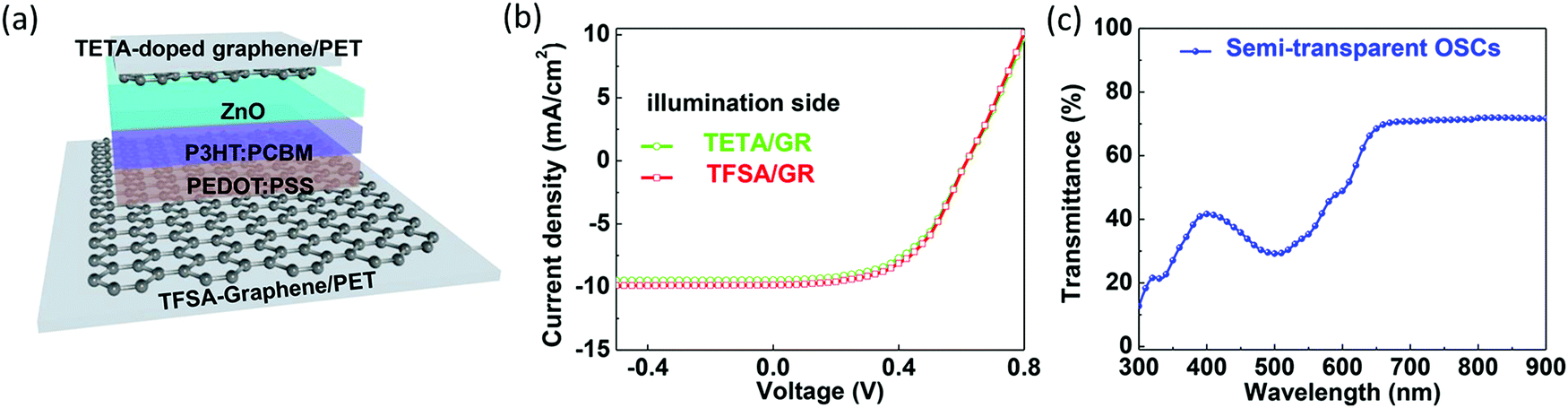 | ||
| Fig. 17 (a) Schematic of the device structure of ST-OSCs with doped-graphene electrodes (both cathode and anode), (b) J–V curve of the flexible device illuminated from different sides, and (c) transmittance spectrum of the ST-OSC.180 Copyright, 2018, ACS. | ||
4. Device engineering
4.1. Ternary bulk-heterojunction structure for ST-OSCs
In the past few years rapid progress has been made in the development of ternary OSCs based on fullerene-free acceptors.183–186 The ternary strategy has been realized as an effective and simple strategy for enhancing the performance of OSCs. The active layer of a ternary structure consists of either two donors and one acceptor (D1:D2:A) or one donor and two acceptors (D:A1:A2).187 It is crucial that the careful selection of the active layer materials provides a broad absorption coverage, resulting in improved photon harvesting and record efficiencies for opaque OSCs. Now, ST-OSCs based on the ternary structure have also become an emerging area of research. The photovoltaic data are presented in Table 2.
Xie et al. reported ternary ST-OSCs with two polymer donors, of PTB7-Th (covering 400–800 nm, Eg = 1.59 eV) and PBT1-S (covering 300–700 nm, Eg = 2.10 eV), and PC71BM as the acceptor.188 The binary device using the PTB7-Th:PC71BM blend gave the highest PCE of 8.0% with an AVT of 20.8%. The addition of 10 wt% of PBT1-S to the PTB7-Th:PC71BM blend in the ITO/PTB7-Th:PBT1-S:PC71BM/Zr(acac)/Ag device achieved an enhanced PCE of 9.2% without sacrificing the AVT and color perception. The devices were optimized using 1,3-propanedithiol (PDT) as the solvent additive. A trade-off between the PCE and the AVT can be seen by lowering the Ag thickness from 15 nm to 5 nm.
Ma et al. prepared a ST-OSC using the PTB-Th donor and two ultra-narrow bandgap acceptors (COi8DFIC, Eg = 1.26 eV; and IEICO-4F, Eg = 1.24 eV) where the optimal concentration of IEICO-4F was maintained at 15 wt%.189 The ST-OSCs were fabricated by varying the thickness of the Ag electrode from 10 to 20 nm. The thin Ag film possesses a high transmittance in the visible region and a low transmittance in the long-wavelength region, which is favorable for photon harvesting in the NIR region with FFAs. The ternary device gave an average PCE of 8.23% with an AVT of 20.78% for 370–740 nm, which is comparable to the COi8DFIC-based binary ST-OSCs (PCE = 7.2%, AVT = 20.25%).
Zhang and co-workers fabricated ternary ST-OSCs using the PTB7-Th donor and two narrow bandgap materials BDTThIT-4F and IEICO-4F as alloyed acceptors.190 The IEICO-4F acceptor with a maximum at 880 nm in the NIR region was used as the third component, complementing the absorption of PTB7-Th and BDTThIT-4F. For ST-OSC fabrication, 1 nm Au/10 nm Ag was used as the top electrode, which exhibited a high transmittance in the visible region from 300 nm to 600 nm. The ST-OSCs with the device structure ITO/PEDOT:PSS/PTB7-Th:BDTThIT-4F:IEICO-4F/PDIN/Au/Ag exhibited a PCE of 9.40% and an AVT of 24.6% from 370 to 740 nm. In comparison, the binary BHJ ST-OSCs using PTB7-Th:BDTThIT-4F and PTB7-Th:IEICO-4F generated PCEs of 7.53 and 8.35% with AVT values of 24.2 and 25.3%, respectively.
Hu et al. successfully employed the ternary strategy to simultaneously enhance the PCE and the AVT of wide bandgap polymer donor-based semitransparent OPVs.191 They introduced the Y6 acceptor with a red-shifted absorption into the D18–Cl:Y6–1O host system. The PCE of opaque OPVs can be enhanced to a best value of 16.05% by introducing 50 wt% Y6, which is mainly due to the improved photon harvesting of the ternary layers. By increasing the Y6 content, the AVT of the active layers is gradually enhanced. The ternary blend film with 50 wt% Y6 realized an AVT of 50.1%. Using Au (1 nm)/Ag (10 nm) as the top electrode, the ST-OSC obtained a PCE of 13.02%, an AVT of 20.2% and a LUE of 2.63%.
Cao and co-workers reported an ST-OSC with the J52:IEICO-4F:PC71BM ternary blend for greenhouse applications.192 The addition of PC71BM suppressed the trap-assisted recombination and enhanced the charge extraction, thus improving the VOC. The ternary ST-OSC achieved a PCE of 8.83% and an AVT of 15.8% using 20-nm-thick Ag. Further reduction of the Ag thickness to 15 and 10 nm lowered the JSC, thus decrease the PCE to 7.75% and 5.93%, and increased the transmittance to 19.9% and 23.7%, respectively, because of less light reflection by the thinner Ag film. Furthermore, the transmission spectra matched well with the absorption of chlorophyll photoreceptors in green plants, making ST-OSCs a viable approach towards light management for plant growth via self-powered greenhouses.
Sano et al. revealed the influence of the blend ratio on the color perception and performance of ST-OSCs. Ternary ST-OSCs were fabricated with the PCDTBT:PC71BM:ITIC BHJ layer sandwiched between a MoO3/Ag/MoO3 top anode and an ITO/ZnO cathode, where the device with an active layer ratio of 1:4:1 exhibited a PCE of 4.0%, an AVT of 39.2% and a CRI value of 97, which is close to the neutral color perception. The device with an active layer ratio of 1:3:1 showed a slight blue color, with a slightly lower PCE of 3.7%, a higher AVT of 44.8% and a lower CRI of 93 (Fig. 18).193
 | ||
| Fig. 18 (a) J−V characteristics of the binary and ternary ST-OSCs with different blend ratios; (b) transmittance (T) and reflectance (R) of the active layer and ternary ST-OSCs; and (c) photographs taken through the 1:3:1 and 1:4:1 ST-OSCs. The lighter areas at the outer ends of the substrates correspond to the electrode-free active layers.193 Copyright, 2019, ACS. (d) J−V characteristics and (e) photographs demonstrating the color tuning using different top electrodes.194 Copyright, 2020, John Wiley and Sons Publishers. | ||
The suitable choice of active layer materials and electrodes is crucial to obtaining a high PCE and keeping suitable visible transparency for energy-generating windows. Wang et al. achieved an excellent PCE of 13.1% whilst still maintaining a high AVT of 22.4% when using a PBDB-TF:Y6:BTTPC ternary blend and a 12-nm-thick Ag anode, compared with a PCE of 12.8% and an AVT of 19.3% for the binary device without BTTPC.194 The two acceptors Y6 and BTTPC formed an alloy model absorbing in the NIR region, improving the transparency in the visible region. When a pair of LiF/MoO3 bilayers on top of an ultrathin Ag electrode was used as an effective photonic reflector layer, the device generated a PCE of 12.3% whilst still maintaining a high AVT of 23.4% (Fig. 18d and e). Zheng et al. obtained the highest recorded PCE of 13.49% with a high AVT of 22.58% for ternary ST-OSCs using a complementary absorbing blend of PBDB-TF:Y6:DTNIF (a dithienonaphthalene-based acceptor) and a 15 nm Ag top electrode with good visible-light transparency (Fig. 19).195 An opaque device with the same configuration generated a PCE of 16.73%. With a lower thickness of 10 nm, the device gave a PCE of 12.1% and AVT of 25.9%, while further increase in thickness resulted in an increase in PCE to 14.5% with lower AVT of 19.78%.
 | ||
| Fig. 19 (a and b) Normalized absorption spectra of pristine PBDB-TF, DTNIF, and Y6 films; (b) energy level diagram of the device components; and (c) photograph of the ST-OSC.195 Copyright 2020, Royal Society of Chemistry. | ||
4.2. Tandem structure for ST-OSCs
In tandem solar cells, two or more solar cells are stacked together to utilize more of the solar spectrum. The tandem strategy becomes an efficient solution by combining the different subcells together. The tandem cell approach has also been used in ST-OSCs to make them more efficient. In the tandem structure using PBDTT-FDPP-C12 in the front subcell and PBDTT-SeDPP in the rear subcell, the device achieved an improved PCE of 7.3%, a high VOC of 1.47 V, and an AVT of 30%.121 Meiss et al. fabricated tandem ST-OSCs by stacking two subcells with complementary absorbing F4-ZnPc and DCV6T as donors and C60 as the acceptor. The tandem cell exhibits a PCE of 4.9 ± 0.2% with a 24% AVT.196 Al/Ag was used as top contact, over which a 90-nm-thick Alq3 layer was used to increase the light out-coupling (Fig. 20). | ||
| Fig. 20 (a) Chemical structures of the absorber materials F4-ZnPc, DCV6T, and C60; (b) schematic of the tandem solar cell; and (c) a photograph of the devices.196 Copyright 2011, AIP Publishers. | ||
The PCEs of tandem ST-OSCs with TQ1:PC71BM and P3TI:PC71BM as front and rear subcells demonstrated improved PCEs of 5.29% and 5.63% in parallel and series configurations, respectively. The tandem cell outperformed the PCEs of single-junction ST-OSCs by about 50% whilst still maintaining a high transmittance of ∼25%. The overall loss of photons in the ST tandem OSC due to parasitic absorption, reflection and transmission can be lower than the loss in a single-junction solar cell using the same absorber materials.105 In parallel connection, the JSC of the tandem cell is the addition of the JSC values of two subcells, while the VOC is the average of each subcell. However, the JSC obtained in the series connection is constant throughout the device, and thus lower than for the parallel connection. In a series connection the VOC is the sum of two subcells. Chang et al. used the same polymer donor PIDT-phanQ with the PC61BM or PC71BM acceptors in different subcells to prepare efficient tandem ST-OSCs. The device using a MoO3/Ag top electrode achieved a PCE of 7.4% with a high AVT of 40% and a CRI approaching ∼100.197
Chen et al. prepared a tandem ST-OSC using a narrow band gap fullerene-free acceptor IEICS-4F absorbing up to 1000 nm blended with the PTB7-Th polymer donor in the rear subcell. The front cell consists of a medium bandgap acceptor FTTB-PDI4 blended with the P3TEA polymer. The tandem device has a broad absorption from 300 nm to 1000 nm. The device structure of glass/ITO/ZnO/P3TEA:FTTB-PDI4/PEDOT:PSS/ZnO/PTB7-Th:IEICS-4F/MoO3/Au was used to fabricate a series of tandem ST-OSCs, which exhibited a high PCE of 10.5% with an AVT of 20%.198 Yusoff et al. used solution-processed graphene mesh as the ST anode and laminated AgNWs as the ST cathode in tandem OSCs. The front subcell was made using a wide bandgap PSEHTT:IC60BA blend, while the rear subcell was made with a narrow bandgap PBDTT-DPP:PC71BM blend. ST-OSCs illuminated from either the graphene mesh or laminated AgNWs sides obtained PCEs of 8.02% and 6.47%, respectively, with a visible transparency of about 45%.199
4.3. Photonic crystals for ST-OSCs
Photonic crystals (PCs) are periodic dielectric nanostructures that are designed to establish the energy band structure for photons, allowing or prohibiting the transmission of photons over certain wavelength ranges. They can be applied as a one dimensional (1D) photonic crystal (1DPC), a dielectric mirror or a distributed Bragg reflector in ST-OSCs to boost their performance. The dielectric mirror is able to manage the photons and resolves the trade-off between the PCE and the AVT in ST-OSCs. When the photon energy is smaller than the photonic band gap of a 1DPC, the photons will be reflected. The operating concept of distributed Bragg reflectors and dielectric mirrors is based on the constructive interference of multilayer dielectric films. They are all made up of multilayer dielectric films with varying refractive indices. The data are presented in Table 3.In 2012 Yu et al. used 8 pairs of high-refractive-index (WO3)/low-refractive-index (LiF) in 1DPC, which act as a distributed reflector in ST-OSCs. The use of 1DPC improved the PCE of the P3HT:PC61BM device from 2.04% to 2.58%.200 The AVT using 1DPC was almost zero for the 400–600 nm range, suggesting sufficient light absorption by the active layer. In 2015, the same group reported neutral colored binary ST-OSCs based on PCDTBT:PC71BM by using 5 pairs of 1DPCs consisting of [MoO3/LiF]pair which exhibited PCE of 5.31 and AVT of 25.1% and CRI close to 97.50
Martorell's group used a photonic crystal based on a multilayer MoO3/LiF to trap the near-infrared and near-ultraviolet photons and to improve the device transparency in PTB7:PC71BM-based OSCs.201 The PC was grown on top of a thin Ag electrode. Use of the photonic crystal improved the JSC by about 26% compared with the cell without the PC layer whilst still maintaining a visible transparency close to 30% and a PCE of 5.6%. The JSC of the transparent cell (10.9 mA cm−2) is about 77% lower compared with the opaque cell. In 2017, Li and co-workers designed an inverted ST-OSC using the PTB7-Th:PC71BM active layer and six pairs of MoO3/LiF-based 1DPCs, which exhibited a PCE of 7.0% with an AVT of 12.2%.202 When P3HT or PTB7 was used as the donor, the device PCE was reduced to 3.2% and 6.4% with an AVT of 19.0 and 16.9%, respectively.
ST-OSCs prepared using the PTB7:PC71BM blend, and six layers of 1DPC, made up of alternating TiO2 and SiO2, were incorporated between the Au and glass substrate to maximize the current while maintaining the overall visible transparency of the OSC above 20%. An antireflection coating of MoO3/LiF was deposited over the Ag cathode and ZnO was used as the ETL.203 The ST-OSC gave a PCE of 5.3% which is about 90% of the analogous opaque device with an AVT of 21.4%. The group of Brabec and Cao developed an optical model to design 1DPCs for high-performance ST-OSCs.204 Two pairs of 1DPC [MoO3/LiF] were deposited over the thin Ag layer to improve the optical properties. The binary ST-OSC based on PTB7-Th:IEICO-4F reached a PCE of 10.83% and an AVT of 29.5%.
Yu et al. introduced five pairs of [WO3/LiF] as a 1DPC to develop a neutral color P3HT:ICBA-based ST-OSC with high PCE and CRI values. The P3HT-based device generally absorbs in the green-light region showing a crimson color with a low CRI value. A simultaneous increase in PCE and lowering of the AVT was observed by increasing the number of 1DPCs. The strong reflection of the 1DPC levels up the transmittance spectrum induced in the weak absorption region of the P3HT:ICBA. With 5 pairs of 1DPC, the device gave a PCE of 5.12% with an AVT of 24.4%. The CRI value increased from 79 (without 1DPC) to 89 (with 5 pairs of 1DPC).205 Shen et al. developed a ST-OSC using 1DPC [WO3/LiF]5 and the PTB7-Th:PC71BM active layer, yielding a PCE of up to 9.36% and an AVT of 14.31%.206 The EQE spectra were enhanced in the 540 nm to 700 nm region due to the enhancement in the reflection by the WO3/[WO3/LiF]5 layer. Therefore, light management via the introduction of photonic crystals has significant importance for management of the color purity and performance of ST-OSCs.
Zhang et al. reported that the ternary neutral-colored ST-OSC with a CRI approaching 100 makes it useful for BIPV applications (as shown in Fig. 21).207 The device was fabricated with three layers of MoO3/LiF as a photonic crystal or DM with the structure of ITO/PEDOT:PSS/J71:PTB7-Th:IHIC/PDINO/Au/Ag/DM. The PCE is increased from 8.93% to 9.37% compared with the reference device without the DM, while the AVT was lowered substantially from 24.4% to 21.4%. Meanwhile, the CRI of the ternary ST-OSCs is 97, with a CIE of (0.3200,0.3287) and a correlative color temperature (CCT) of 5931 K.
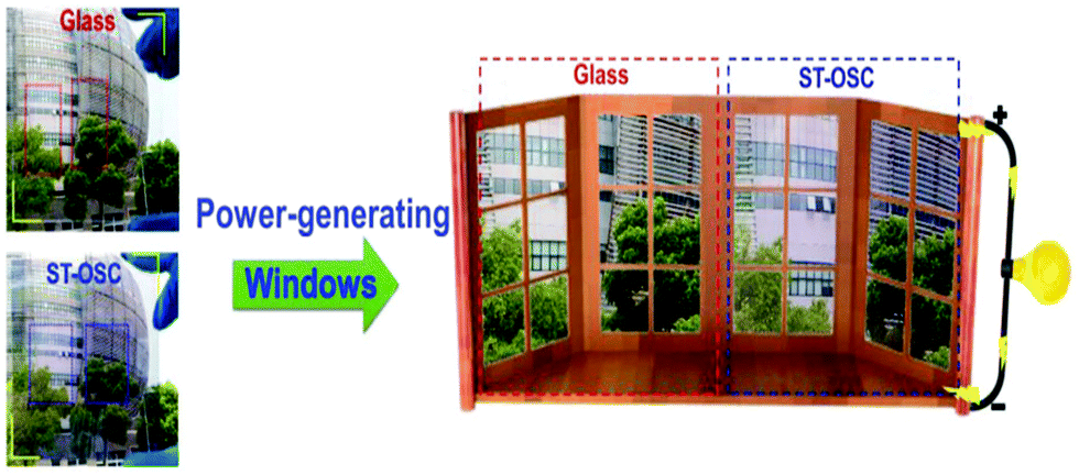 | ||
| Fig. 21 Left: digital photographs of the J71:PTB7-Th:IHIC-based ternary ST-OSC and its glass counterpart. Right: Devices used as glass applied to windows.207 Copyright, 2019, John Wiley and Sons. | ||
Li et al. developed a new photonic crystal consisting of LiF/TeO2/LiF/TeO2 dielectric multilayers as a transparent electrode and photon reflector.208 The ST-OSC achieved a PCE 7.3% and an AVT value of 29.5% suggesting excellent multifunctional ST-OSCs for window applications. They have further developed high-efficiency variable-color ST-OSCs via optical modulation using an Ag/TeO2/Ag Fabry–Pérot electrode.209 The devices with the ITO/PEDOT:PSS/PBDB-TF:Y6/Bis-FIMG/Ag/TeO2/Ag structure generated an excellent tunable color with PCEs of >14% and a maximum transmittance of up to 31%.
5. Potential applications and future perspective
Research in the field of solution-processable flexible and robust ST-OSCs has made significant progress in the past decade with the development of new materials, transparent electrode designs, interfacial layer processing and device engineering. The performance of ST-OSCs has been significantly improved, which makes them a strong contender for commercial applications such as in BIPV devices, power windows, indoor photovoltaics, automobile sun-rooves with variable color and transparency, and agrivoltaics.78,210–212 BIPV devices using ST-OSCs act as a power-generating source as well as lighting up the building interior via the transmission of light. One of the attractive features of ST-OSCs is their variable color and transparency.76,160 The color selection and transparency are the major focus of future technology and will depending on the end user's applications. As the technology progresses, there will be a strong requirement for color selection and quality, which can be easily tuned via bandgap modulation using an appropriate molecular design or via device optical engineering with dielectric structures.The integration of ST-OSCs for agrivoltaics, i.e., in greenhouse-based agriculture, provides additional energy for crop growth and offers a high production rate.213,214 The ST-OSCs for agricultural applications must be adaptable to the solar spectrum in response to plant photomorphogenesis. The light within the blue region enables vegetative leaf growth while the light within the red region facilitates flower growth.215 Song et al. reported flexible ST-OSCs that use the PBDB-T-2F:Y6 photoactive layer absorbing in the NIR region and a modified PEDOT:PSS electrode, achieving over 10% PCE and 21% AVT for use in agricultural plant growth.111 Therefore, the proper choice of material combinations can develop efficient ST-OSCs with longer lifetimes for power-generating greenhouse applications.153,192 Colsmann and co-workers reported the potential application of ST-OSCs in wearable electronics, such as solar-powered sunglasses.216 Although the applications of ST-OSCs are currently in their initial stage, they will play a key role in the future photovoltaic technology. It is also important to find out the appropriate conditions for low-temperature processing for the development of flexible ST-OSCs.
6. Conclusion
Opaque and semitransparent OSCs, as a new photovoltaic technology, have complemented silicon-based photovoltaics well, with current efficiencies reaching 18% and 13%, respectively. ST-OSCs as power-generating windows will not only generate power but will also create beautiful, pleasant and heat-controlled surroundings in buildings. By choosing the appropriate semitransparent top electrode, active layer, and device structure of a ST-OSC, a high PCE and AVT can be obtained. In this review, we focused on summarizing the recent developments in each component of the ST-OSC device, such as the top electrode, active layer materials, carrier-transport layer and device engineering. Despite the fact that the PCEs of ST-OSCs have climbed to ∼13%, they have been achieved at the expense of poor AVT values. The well-balanced PCE and AVT of semitransparent OSCs remains a major issue, and much attention should be devoted to the synthesis of organic materials, active layer design, semitransparent top electrodes, optical modeling, device engineering, and stability. The recent improvements have mainly been due to the development of fullerene-free acceptors and new polymer donors that enable simultaneously high PCE and AVT values to be maintained. Although some high-performance devices have been reported for binary and ternary devices, achieving a PCE of >12% and an AVT reaching 25%, which is the requirement for window applications, rooms for further improvement remains. New molecular designs, morphology and device structure optimizations could further enhance the efficiency and transparency for practical applications in building-integrated photovoltaics and glass windows for vehicles.To fabricate highly efficient ST-OSCs, the materials must have a strong absorption in the near-infrared range and high transmittance in the visible-light region. In terms of that, a ternary structure can be one of the preferred compositions for improving photon harvesting of active layers in the near-infrared region. The photon-harvesting ability is also influenced by the chemical composition of the photoactive layers, especially in the long-wavelength region. The photon harvesting of active layers in the visible and near-infrared ranges may also be adjusted by changing the D:A ratio, optimizing the active layer thickness, and the addition of a bilayer structure, all of which have been shown to be effective ways of increasing the AVT of ST-OSCs.
ST-OSCs also require a transparent top electrode with high conductivity and transmittance in the visible-light region and high reflectance in the near-infrared region, in addition to the materials used in the active layers. The transmittance of the top electrode is crucial for calculating the AVT of ST-OSCs. To achieve a good balance between conductivity and transmittance, the thickness of a semitransparent electrode must be carefully optimized. Meanwhile, the optimal semitransparent top electrodes should be compatible with the bottom active layer, fabricated using simple solution processing. To achieve selective transmittance and reflection for the simultaneous improvement of the PCE and AVT values of ST-OSCs, photonic crystals, antireflection coatings, optical microcavities, and DMD structures have also been used. However, because of their complicated device structure, the cost of the ST-OSCs could increase. Some thin metal electrodes including Au, Ag, and AgNWs with high transmittance have been implemented, although their high reflectance can be unfavorable for the device performance. As a result, semitransparent top electrodes with the necessary optical, electrical, and processing properties, as well as being low cost and having high stability, should be investigated further for constructing highly efficient ST-OSCs. Other carbon-based electrode materials have also been used, but they have low transparency and conductivity, therefore limiting the performance of ST-OSCs. Many efforts are required, and include material selection, active layer optimization to improve the photon-usage efficiency, and semitransparent electrode design to concurrently enhance the PCE and AVT for efficient ST-OSCs. Finally, studies on device stability will need special attention in the future. We anticipate considerable advancements in both the electrical and optical performance in the near future. As a result, we believe that ST-OSCs, with their unique flexibility and great optical and electrical performance, have a bright future in the solar industry.
Conflicts of interest
There are no conflicts to declare.Acknowledgements
The authors thank the Department of Science and Technology (DST), New Delhi (DST/TMD/SERI/D05 G), for financial support. KK thanks DST for awarding the DST-INSPIRE fellowship.References
- K. A. Mazzio and C. K. Luscombe, Chem. Soc. Rev., 2015, 47, 78–90 RSC.
- J. Roncali, Acc. Chem. Res., 2009, 42, 1719–1730 CrossRef CAS PubMed.
- V. V. Brus, J. Lee, B. Luginbuhl, S.-J. Ko, G. C. Bazan and T.-Q. Nguyen, Adv. Mater., 2019, 31, 1900904 CrossRef PubMed.
- C. Peng, Y. Huang and Z. Wu, Energy Build., 2011, 43, 3592–3598 CrossRef.
- K. Forberich, F. Guo, C. Bronnbauer and C. J. Brabec, Energy Technol., 2015, 3, 1051–1058 CrossRef CAS.
- C. J. Traverse, R. Pandey, M. C. Barr and R. R. Lunt, Nat. Energy, 2017, 2, 849–860 CrossRef.
- C. Ballif, L.-E. Perret-Aebi, S. Lufkin and E. Rey, Nat. Energy, 2018, 3, 438–442 CrossRef.
- A. Mishra and P. Bäuerle, Angew. Chem., Int. Ed., 2012, 51, 2020–2067 CrossRef CAS.
- A. Mishra, Energy Environ. Sci., 2020, 13, 4738–4793 RSC.
- Y. Cui, H. Yao, L. Hong, T. Zhang, Y. Tang, B. Lin, K. Xian, B. Gao, C. An, P. Bi, W. Ma and J. Hou, Natl. Sci. Rev., 2019, 7, 1239–1246 CrossRef PubMed.
- H. Kang, G. Kim, J. Kim, S. Kwon, H. Kim and K. Lee, Adv. Mater., 2016, 28, 7821–7861 CrossRef CAS PubMed.
- M. Kaltenbrunner, M. S. White, E. D. Głowacki, T. Sekitani, T. Someya, N. S. Sariciftci and S. Bauer, Nat. Commun., 2012, 3, 770 CrossRef PubMed.
- R. Søndergaard, M. Hösel, D. Angmo, T. T. Larsen-Olsen and F. C. Krebs, Mater. Today, 2012, 15, 36–49 CrossRef.
- Y. Zhang, Z. Peng, C. Cai, Z. Liu, Y. Lin, W. Zheng, J. Yang, L. Hou and Y. Cao, J. Mater. Chem. A, 2016, 4, 11821–11828 RSC.
- S.-Y. Chang, P. Cheng, G. Li and Y. Yang, Joule, 2018, 2, 1039–1054 CrossRef CAS.
- Y. Li, G. Xu, C. Cui and Y. Li, Adv. Energy Mater., 2018, 8, 1701791 CrossRef.
- Q. Tai and F. Yan, Adv. Mater., 2017, 29, 1700192 CrossRef.
- Z. Hu, J. Wang, X. Ma, J. Gao, C. Xu, K. Yang, Z. Wang, J. Zhang and F. Zhang, Nano Energy, 2020, 78, 105376 CrossRef CAS.
- C.-C. Chueh, S.-C. Chien, H.-L. Yip, J. F. Salinas, C.-Z. Li, K.-S. Chen, F.-C. Chen, W.-C. Chen and A. K. Y. Jen, Adv. Energy Mater., 2013, 3, 417–423 CrossRef CAS.
- C. Guo, D. Li, L. Wang, B. Du, Z.-X. Liu, Z. Shen, P. Wang, X. Zhang, J. Cai, S. Cheng, C. Yu, H. Wang, D. Liu, C.-Z. Li and T. Wang, Adv. Energy Mater., 2021, 2102000 CrossRef CAS.
- C. Li, J. Zhou, J. Song, J. Xu, H. Zhang, X. Zhang, J. Guo, L. Zhu, D. Wei, G. Han, J. Min, Y. Zhang, Z. Xie, Y. Yi, H. Yan, F. Gao, F. Liu and Y. Sun, Nat. Energy, 2021, 6, 605–613 CrossRef CAS.
- F. Liu, L. Zhou, W. Liu, Z. Zhou, Q. Yue, W. Zheng, R. Sun, W. Liu, S. Xu, H. Fan, L. Feng, Y. Yi, W. Zhang and X. Zhu, Adv. Mater., 2021, 2100830 CrossRef CAS PubMed.
- Y. Lin, M. I. Nugraha, Y. Firdaus, A. D. Scaccabarozzi, F. Aniés, A.-H. Emwas, E. Yengel, X. Zheng, J. Liu, W. Wahyudi, E. Yarali, H. Faber, O. M. Bakr, L. Tsetseris, M. Heeney and T. D. Anthopoulos, ACS Energy Lett., 2020, 3663–3671 CrossRef CAS.
- Y. Cui, H. Yao, J. Zhang, K. Xian, T. Zhang, L. Hong, Y. Wang, Y. Xu, K. Ma, C. An, C. He, Z. Wei, F. Gao and J. Hou, Adv. Mater., 2020, 32, 1908205 CrossRef CAS PubMed.
- S. Dai and X. Zhan, Adv. Energy Mater., 2018, 8, 1800002 CrossRef.
- S. Yoon, S. Tak, J. Kim, Y. Jun, K. Kang and J. Park, Build. Environ., 2011, 46, 1899–1904 CrossRef.
- P. Selvaraj, A. Ghosh, T. K. Mallick and S. Sundaram, Renewable Energy, 2019, 141, 516–525 CrossRef.
- A. Agrawal, S. A. Siddiqui, A. Soni, K. Khandelwal and G. D. Sharma, Sol. Energy, 2021, 226, 9–19 CrossRef CAS.
- A. Roy, A. Ghosh, S. Bhandari, P. Selvaraj, S. Sundaram and T. K. Mallick, J. Phys. Chem. C, 2019, 123, 23834–23837 CrossRef CAS.
- L. Kavan, J.-H. Yum and M. Graetzel, ACS Appl. Mater. Interfaces, 2012, 4, 6999–7006 CrossRef CAS.
- G. H. Rao, P. J. S. Rana, A. Islam and S. P. Singh, ACS Appl. Energy Mater., 2018, 1, 4786–4793 CrossRef CAS.
- W. Naim, V. Novelli, I. Nikolinakos, N. Barbero, I. Dzeba, F. Grifoni, Y. Ren, T. Alnasser, A. Velardo, R. Borrelli, S. Haacke, S. M. Zakeeruddin, M. Graetzel, C. Barolo and F. Sauvage, JACS Au, 2021, 1, 409–426 CrossRef CAS.
- M. Godfroy, J. Liotier, V. M. Mwalukuku, D. Joly, Q. Huaulmé, L. Cabau, C. Aumaitre, Y. Kervella, S. Narbey, F. Oswald, E. Palomares, C. A. González Flores, G. Oskam and R. Demadrille, Sustainable Energy Fuels, 2021, 5, 144–153 RSC.
- J. Burschka, N. Pellet, S.-J. Moon, R. Humphry-Baker, P. Gao, M. K. Nazeeruddin and M. Grätzel, Nature, 2013, 499, 316–319 CrossRef CAS PubMed.
- M. A. Green, A. Ho-Baillie and H. J. Snaith, Nat. Photon., 2014, 8, 506–514 CrossRef CAS.
- W. S. Yang, B.-W. Park, E. H. Jung, N. J. Jeon, Y. C. Kim, D. U. Lee, S. S. Shin, J. Seo, E. K. Kim, J. H. Noh and S. I. Seok, Science, 2017, 356, 1376–1379 CrossRef CAS.
- S. Rahmany and L. Etgar, ACS Energy Lett., 2020, 5, 1519–1531 CrossRef CAS.
- M. Mujahid, C. Chen, J. Zhang, C. Li and Y. Duan, InfoMat, 2021, 3, 101–124 CrossRef CAS.
- P. You, Z. Liu, Q. Tai, S. Liu and F. Yan, Adv. Mater., 2015, 27, 3632–3638 CrossRef CAS PubMed.
- C. Roldán-Carmona, O. Malinkiewicz, R. Betancur, G. Longo, C. Momblona, F. Jaramillo, L. Camacho and H. J. Bolink, Energy Environ. Sci., 2014, 7, 2968–2973 RSC.
- L. Yuan, Z. Wang, R. Duan, P. Huang, K. Zhang, Q. Chen, N. K. Allam, Y. Zhou, B. Song and Y. Li, J. Mater. Chem. A, 2018, 6, 19696–19702 RSC.
- G. E. Eperon, V. M. Burlakov, A. Goriely and H. J. Snaith, ACS Nano, 2014, 8, 591–598 CrossRef CAS PubMed.
- K.-T. Lee, M. Fukuda, S. Joglekar and L. J. Guo, J. Mater. Chem. C, 2015, 3, 5377–5382 RSC.
- J.-H. Lu, Y.-L. Yu, S.-R. Chuang, C.-H. Yeh and C.-P. Chen, J. Phys. Chem. C, 2016, 120, 4233–4239 CrossRef CAS.
- B.-X. Chen, H.-S. Rao, H.-Y. Chen, W.-G. Li, D.-B. Kuang and C.-Y. Su, J. Mater. Chem. A, 2016, 4, 15662–15669 RSC.
- K.-S. Chen, J.-F. Salinas, H.-L. Yip, L. Huo, J. Hou and A. K. Y. Jen, Energy Environ. Sci., 2012, 5, 9551–9557 RSC.
- C. Yang, D. Liu, M. Bates, M. C. Barr and R. R. Lunt, Joule, 2019, 3, 1803–1809 CrossRef.
- T. Ameri, G. Dennler, C. Waldauf, H. Azimi, A. Seemann, K. Forberich, J. Hauch, M. Scharber, K. Hingerl and C. J. Brabec, Adv. Funct. Mater., 2010, 20, 1592–1598 CrossRef CAS.
- N. Lynn, L. Mohanty and S. Wittkopf, Build. Environ., 2012, 54, 148–158 CrossRef.
- W. Yu, X. Jia, Y. Long, L. Shen, Y. Liu, W. Guo and S. Ruan, ACS Appl. Mater. Interfaces, 2015, 7, 9920–9928 CrossRef CAS PubMed.
- Y. Li, C. He, L. Zuo, F. Zhao, L. Zhan, X. Li, R. Xia, H.-L. Yip, C.-Z. Li, X. Liu and H. Chen, Adv. Energy Mater., 2021, 11, 2003408 CrossRef CAS.
- H. Xu, F. Yuan, D. Zhou, X. Liao, L. Chen and Y. Chen, J. Mater. Chem. A, 2020, 8, 11478–11492 RSC.
- J. Meyer, S. Hamwi, M. Kröger, W. Kowalsky, T. Riedl and A. Kahn, Adv. Mater., 2012, 24, 5408–5427 CrossRef CAS PubMed.
- M. D. Irwin, D. B. Buchholz, A. W. Hains, R. P. H. Chang and T. J. Marks, Proc. Natl. Acad. Sci. U. S. A., 2008, 105, 2783–2787 CrossRef CAS.
- S. Han, W. S. Shin, M. Seo, D. Gupta, S.-J. Moon and S. Yoo, Org. Electron., 2009, 10, 791–797 CrossRef CAS.
- X. Gu, W. Cui, H. Li, Z. Wu, Z. Zeng, S.-T. Lee, H. Zhang and B. Sun, Adv. Energy Mater., 2013, 3, 1262–1268 CrossRef CAS.
- X. Fan, W. Nie, H. Tsai, N. Wang, H. Huang, Y. Cheng, R. Wen, L. Ma, F. Yan and Y. Xia, Adv. Sci., 2019, 6, 1900813 CrossRef CAS.
- H. Zhou, Y. Zhang, C.-K. Mai, J. Seifter, T.-Q. Nguyen, G. C. Bazan and A. J. Heeger, ACS Nano, 2015, 9, 371–377 CrossRef CAS.
- S.-S. Li, K.-H. Tu, C.-C. Lin, C.-W. Chen and M. Chhowalla, ACS Nano, 2010, 4, 3169–3174 CrossRef CAS.
- M. S. White, D. C. Olson, S. E. Shaheen, N. Kopidakis and D. S. Ginley, Appl. Phys. Lett., 2006, 89, 143517 CrossRef.
- T. Z. Oo, R. Devi Chandra, N. Yantara, R. R. Prabhakar, L. H. Wong, N. Mathews and S. G. Mhaisalkar, Org. Electron., 2012, 13, 870–874 CrossRef CAS.
- J. Wei, Z. Yin, S.-C. Chen and Q. Zheng, ACS Appl. Mater. Interfaces, 2017, 9, 6186–6193 CrossRef CAS PubMed.
- C. Waldauf, M. Morana, P. Denk, P. Schilinsky, K. Coakley, S. A. Choulis and C. J. Brabec, Appl. Phys. Lett., 2006, 89, 233517 CrossRef.
- H.-H. Liao, L.-M. Chen, Z. Xu, G. Li and Y. Yang, Appl. Phys. Lett., 2008, 92, 173303 CrossRef.
- Z. Yin, J. Wei, S.-C. Chen, D. Cai, Y. Ma, M. Wang and Q. Zheng, J. Mater. Chem. A, 2017, 5, 3888–3899 RSC.
- T. Jiang, G. Zhang, R. Xia, J. Huang, X. Li, M. Wang, H. L. Yip and Y. Cao, Mater. Today Energy, 2021, 21, 100807 CrossRef CAS.
- J. You, C.-C. Chen, Z. Hong, K. Yoshimura, K. Ohya, R. Xu, S. Ye, J. Gao, G. Li and Y. Yang, Adv. Mater., 2013, 25, 3973–3978 CrossRef CAS PubMed.
- J.-H. Choi, H.-J. Choi, J.-H. Shin, H.-P. Kim, J. Jang and H. Lee, Org. Electron., 2013, 14, 3180–3185 CrossRef CAS.
- B. Yang, Y. Bai, R. Zeng, C. Zhao, B. Zhang, J. Wang, T. Hayat, A. Alsaedi and Z. A. Tan, Org. Electron., 2019, 74, 82–88 CrossRef CAS.
- J. Liu, J. Wu, S. Shao, Y. Deng, B. Meng, Z. Xie, Y. Geng, L. Wang and F. Zhang, ACS Appl. Mater. Interfaces, 2014, 6, 8237–8245 CrossRef CAS.
- K. D. Kadam, H. Kim, S. Rehman, H. Patil, J. Aziz, T. D. Dongale, M. F. Khan and D.-K. Kim, Energy Fuels, 2021, 35, 12416–12424 CrossRef CAS.
- F. J. Lim, A. Krishnamoorthy, J. Luther and G. W. Ho, J. Mater. Chem., 2012, 22, 25057–25064 RSC.
- S. Ozcan, M. C. Erer, S. Vempati, T. Uyar, L. Toppare and A. Çırpan, J. Mater. Sci.: Mater. Electron., 2020, 31, 3576–3584 CrossRef CAS.
- Y. W. Han, H. S. Lee and D. K. Moon, ACS Appl. Mater. Interfaces, 2021, 13, 19085–19098 CrossRef CAS PubMed.
- D. K. Chaudhary, P. K. Dhawan, S. P. Patel and H. P. Bhasker, Mater. Lett., 2021, 283, 128725 CrossRef CAS.
- Y. Bai, C. Zhao, X. Chen, S. Zhang, S. Zhang, T. Hayat, A. Alsaedi, Z. A. Tan, J. Hou and Y. Li, J. Mater. Chem. A, 2019, 7, 15887–15894 RSC.
- Y. Bai, C. Zhao, R. Shi, J. Wang, F. Wang, T. Hayat, A. Alsaedi and Z. A. Tan, Mater. Chem. Front., 2020, 4, 2072–2080 RSC.
- G. P. Kini, S. J. Jeon and D. K. Moon, Adv. Funct. Mater., 2021, 31, 2007931 CrossRef CAS.
- J.-J. Shen, Synth. Met., 2021, 271, 116582 CrossRef CAS.
- H. Kim, C. M. Gilmore, A. Piqué, J. S. Horwitz, H. Mattoussi, H. Murata, Z. H. Kafafi and D. B. Chrisey, J. Appl. Phys., 1999, 86, 6451–6461 CrossRef CAS.
- H. Kim, A. Piqué, J. S. Horwitz, H. Mattoussi, H. Murata, Z. H. Kafafi and D. B. Chrisey, Appl. Phys. Lett., 1999, 74, 3444–3446 CrossRef CAS.
- R. Bel Hadj Tahar, T. Ban, Y. Ohya and Y. Takahashi, J. Appl. Phys., 1998, 83, 2631–2645 CrossRef CAS.
- H. Schmidt, H. Flügge, T. Winkler, T. Bülow, T. Riedl and W. Kowalsky, Appl. Phys. Lett., 2009, 94, 243302 CrossRef.
- J. Huang, G. Li and Y. Yang, Adv. Mater., 2008, 20, 415–419 CrossRef CAS.
- A. Colsmann, A. Puetz, A. Bauer, J. Hanisch, E. Ahlswede and U. Lemmer, Adv. Energy Mater., 2011, 1, 599–603 CrossRef CAS.
- J. Hanisch, E. Ahlswede and M. Powalla, Eur. Phys. J.: Appl. Phys., 2007, 37, 261–264 CrossRef CAS.
- A. Bauer, T. Wahl, J. Hanisch and E. Ahlswede, Appl. Phys. Lett., 2012, 100, 073307 CrossRef.
- C. Tao, G. Xie, C. Liu, X. Zhang, W. Dong, F. Meng, X. Kong, L. Shen, S. Ruan and W. Chen, Appl. Phys. Lett., 2009, 95, 053303 CrossRef.
- S. Wilken, V. Wilkens, D. Scheunemann, R.-E. Nowak, K. von Maydell, J. Parisi and H. Borchert, ACS Appl. Mater. Interfaces, 2015, 7, 287–300 CrossRef CAS PubMed.
- J. Yuan, M. Ford, G. Ding, H. Dong, M. Wang, L. Han, Y. Li, G. C. Bazan and W. Ma, J. Mater. Chem. A, 2016, 4, 17333–17343 RSC.
- M. B. Upama, M. Wright, N. K. Elumalai, M. A. Mahmud, D. Wang, K. H. Chan, C. Xu, F. Haque and A. Uddin, Curr. Appl. Phys., 2017, 17, 298–305 CrossRef.
- L. Shen, Y. Xu, F. Meng, F. Li, S. Ruan and W. Chen, Org. Electron., 2011, 12, 1223–1226 CrossRef CAS.
- T. Winkler, H. Schmidt, H. Flügge, F. Nikolayzik, I. Baumann, S. Schmale, T. Weimann, P. Hinze, H.-H. Johannes, T. Rabe, S. Hamwi, T. Riedl and W. Kowalsky, Org. Electron., 2011, 12, 1612–1618 CrossRef CAS.
- M. B. Upama, M. Wright, N. K. Elumalai, M. A. Mahmud, D. Wang, C. Xu and A. Uddin, ACS Photon., 2017, 4, 2327–2334 CrossRef CAS.
- X. Liu, Y. Zhao, J. Yu and R. Zhu, Mater. Chem. Front., 2021, 5, 8197–8205 RSC.
- Y. Zhou, H. Cheun, S. Choi, C. Fuentes-Hernandez and B. Kippelen, Org. Electron., 2011, 12, 827–831 CrossRef CAS.
- R. J. Peh, Y. Lu, F. Zhao, C.-L. K. Lee and W. L. Kwan, Sol. Energy Mater. Sol. Cells, 2011, 95, 3579–3584 CrossRef CAS.
- Q. Dong, Y. Zhou, J. Pei, Z. Liu, Y. Li, S. Yao, J. Zhang and W. Tian, Org. Electron., 2010, 11, 1327–1331 CrossRef CAS.
- L. Groenendaal, F. Jonas, D. Freitag, H. Pielartzik and J. R. Reynolds, Adv. Mater., 2000, 12, 481–494 CrossRef CAS.
- N. Kim, H. Kang, J.-H. Lee, S. Kee, S. H. Lee and K. Lee, Adv. Mater., 2015, 27, 2317–2323 CrossRef CAS PubMed.
- Y. Wang, C. Zhu, R. Pfattner, H. Yan, L. Jin, S. Chen, F. Molina-Lopez, F. Lissel, J. Liu, N. I. Rabiah, Z. Chen, J. W. Chung, C. Linder, M. F. Toney, B. Murmann and Z. Bao, Sci. Adv., 2017, 3, e1602076 CrossRef.
- Y. Xia, K. Sun and J. Ouyang, Adv. Mater., 2012, 24, 2436–2440 CrossRef CAS.
- X. Fan, B. Xu, S. Liu, C. Cui, J. Wang and F. Yan, ACS Appl. Mater. Interfaces, 2016, 8, 14029–14036 CrossRef CAS.
- W. Zheng, Y. Lin, Y. Zhang, J. Yang, Z. Peng, A. Liu, F. Zhang and L. Hou, ACS Appl. Mater. Interfaces, 2017, 9, 44656–44666 CrossRef CAS PubMed.
- Z. Tang, Z. George, Z. Ma, J. Bergqvist, K. Tvingstedt, K. Vandewal, E. Wang, L. M. Andersson, M. R. Andersson, F. Zhang and O. Inganäs, Adv. Energy Mater., 2012, 2, 1467–1476 CrossRef CAS.
- J. Czolk, A. Puetz, D. Kutsarov, M. Reinhard, U. Lemmer and A. Colsmann, Adv. Energy Mater., 2013, 3, 386–390 CrossRef CAS.
- D. J. Lee, D. K. Heo, C. Yun, Y. H. Kim and M. H. Kang, ECS J. Solid State Sci. Technol., 2019, 8, Q32–Q37 CrossRef CAS.
- D. H. Kim, D. J. Lee, B. Kim, C. Yun and M. H. Kang, Solid-State Electron., 2020, 169, 107808 CrossRef CAS.
- X. Fan, B. Xu, N. Wang, J. Wang, S. Liu, H. Wang and F. Yan, Adv. Electron. Mater., 2017, 3, 1600471 CrossRef.
- H. Park, J.-H. Lee, S. Lee, S. Y. Jeong, J. W. Choi, C.-L. Lee, J.-H. Kim and K. Lee, ACS Appl. Mater. Interfaces, 2020, 12, 2276–2284 CrossRef CAS PubMed.
- W. Song, B. Fanady, R. Peng, L. Hong, L. Wu, W. Zhang, T. Yan, T. Wu, S. Chen and Z. Ge, Adv. Energy Mater., 2020, 10, 2000136 CrossRef CAS.
- Y. Wang, B. Jia, F. Qin, Y. Wu, W. Meng, S. Dai, Y. Zhou and X. Zhan, Polymer, 2016, 107, 108–112 CrossRef CAS.
- Z. Ding, V. Stoichkov, M. Horie, E. Brousseau and J. Kettle, Sol. Energy Mater. Sol. Cells, 2016, 157, 305–311 CrossRef CAS.
- J. Krantz, T. Stubhan, M. Richter, S. Spallek, I. Litzov, G. J. Matt, E. Spiecker and C. J. Brabec, Adv. Funct. Mater., 2013, 23, 1711–1717 CrossRef CAS.
- Y.-J. Kang, D.-G. Kim, J.-K. Kim, W.-Y. Jin and J.-W. Kang, Org. Electron., 2014, 15, 2173–2177 CrossRef CAS.
- M. Reinhard, R. Eckstein, A. Slobodskyy, U. Lemmer and A. Colsmann, Org. Electron., 2013, 14, 273–277 CrossRef CAS.
- J.-Y. Lee, S. T. Connor, Y. Cui and P. Peumans, Nano Lett., 2010, 10, 1276–1279 CrossRef CAS PubMed.
- F. Guo, P. Kubis, T. Przybilla, E. Spiecker, A. Hollmann, S. Langner, K. Forberich and C. J. Brabec, Adv. Energy Mater., 2015, 5, 1401779 CrossRef.
- H. Lu, J. Lin, N. Wu, S. Nie, Q. Luo, C.-Q. Ma and Z. Cui, Appl. Phys. Lett., 2015, 106, 093302 CrossRef.
- W. Gaynor, G. F. Burkhard, M. D. McGehee and P. Peumans, Adv. Mater., 2011, 23, 2905–2910 CrossRef CAS PubMed.
- C.-C. Chen, L. Dou, J. Gao, W.-H. Chang, G. Li and Y. Yang, Energy Environ. Sci., 2013, 6, 2714–2720 RSC.
- F. Guo, X. Zhu, K. Forberich, J. Krantz, T. Stubhan, M. Salinas, M. Halik, S. Spallek, B. Butz, E. Spiecker, T. Ameri, N. Li, P. Kubis, D. M. Guldi, G. J. Matt and C. J. Brabec, Adv. Energy Mater., 2013, 3, 1062–1067 CrossRef CAS.
- F. Guo, P. Kubis, T. Stubhan, N. Li, D. Baran, T. Przybilla, E. Spiecker, K. Forberich and C. J. Brabec, ACS Appl. Mater. Interfaces, 2014, 6, 18251–18257 CrossRef CAS PubMed.
- J. H. Yim, S.-y. Joe, C. Pang, K. M. Lee, H. Jeong, J.-Y. Park, Y. H. Ahn, J. C. de Mello and S. Lee, ACS Nano, 2014, 8, 2857–2863 CrossRef CAS PubMed.
- C.-C. Chen, L. Dou, R. Zhu, C.-H. Chung, T.-B. Song, Y. B. Zheng, S. Hawks, G. Li, P. S. Weiss and Y. Yang, ACS Nano, 2012, 6, 7185–7190 CrossRef CAS.
- J. Min, C. Bronnbauer, Z.-G. Zhang, C. Cui, Y. N. Luponosov, I. Ata, P. Schweizer, T. Przybilla, F. Guo, T. Ameri, K. Forberich, E. Spiecker, P. Bäuerle, S. A. Ponomarenko, Y. Li and C. J. Brabec, Adv. Funct. Mater., 2016, 26, 4543–4550 CrossRef CAS.
- J. Czolk, D. Landerer, M. Koppitz, D. Nass and A. Colsmann, Adv. Mater. Technol., 2016, 1, 1600184 CrossRef.
- Z. M. Beiley, M. G. Christoforo, P. Gratia, A. R. Bowring, P. Eberspacher, G. Y. Margulis, C. Cabanetos, P. M. Beaujuge, A. Salleo and M. D. McGehee, Adv. Mater., 2013, 25, 7020–7026 CrossRef CAS PubMed.
- M. Koppitz, E. Wegner, T. Rödlmeier and A. Colsmann, Energy Technol., 2018, 6, 1275–1282 CrossRef CAS.
- H. Zhai, Y. Li, L. Chen, X. Wang, L. Shi, R. Wang and J. Sun, Nano Res., 2018, 11, 1956–1966 CrossRef CAS.
- G. Ji, Y. Wang, Q. Luo, K. Han, M. Xie, L. Zhang, N. Wu, J. Lin, S. Xiao, Y.-Q. Li, L.-Q. Luo and C.-Q. Ma, ACS Appl. Mater. Interfaces, 2018, 10, 943–954 CrossRef CAS PubMed.
- L. Zheng, M. Li, S. Dai, Y. Wu, Y. Cai, X. Zhu, S. Ma, D. Yun and J.-F. Li, J. Phys. Chem. C, 2021, 125, 18623–18629 CrossRef CAS.
- T. Sannicolo, W. H. Chae, J. Mwaura, V. Bulović and J. C. Grossman, ACS Appl. Energy Mater., 2021, 4, 1431–1441 CrossRef CAS.
- R. R. Lunt and V. Bulovic, Appl. Phys. Lett., 2011, 98, 113305 CrossRef.
- J. Meiss, F. Holzmueller, R. Gresser, K. Leo and M. Riede, Appl. Phys. Lett., 2011, 99, 193307 CrossRef.
- H. Zhang, G. Wicht, C. Gretener, M. Nagel, F. Nüesch, Y. Romanyuk, J.-N. Tisserant and R. Hany, Sol. Energy Mater. Sol. Cells, 2013, 118, 157–164 CrossRef CAS.
- Y. Song, K. Zhang, S. Dong, R. Xia, F. Huang and Y. Cao, ACS Appl. Mater. Interfaces, 2020, 12, 18473–18481 CrossRef CAS.
- G. Li, C. W. Chu, V. Shrotriya, J. Huang and Y. Yang, Appl. Phys. Lett., 2006, 88, 253503 CrossRef.
- X. Yang, P. Gao, Z. Yang, J. Zhu, F. Huang and J. Ye, Sci. Rep., 2017, 7, 44576 CrossRef CAS.
- S. Schubert, J. Meiss, L. Müller-Meskamp and K. Leo, Adv. Energy Mater., 2013, 3, 438–443 CrossRef CAS.
- L. Ke, S. C. Lai, H. Liu, C. K. N. Peh, B. Wang and J. H. Teng, ACS Appl. Mater. Interfaces, 2012, 4, 1247–1253 CrossRef CAS.
- H. Shi, R. Xia, C. Sun, J. Xiao, Z. Wu, F. Huang, H.-L. Yip and Y. Cao, Adv. Energy Mater., 2017, 7, 1701121 CrossRef.
- Y. Q. Wong, H.-F. Meng, H. Y. Wong, C. S. Tan, C.-Y. Wu, P.-T. Tsai, C.-Y. Chang, S.-F. Horng and H.-W. Zan, Org. Electron., 2017, 43, 196–206 CrossRef CAS.
- M. Zhang, X. Guo, W. Ma, H. Ade and J. Hou, Adv. Mater., 2015, 27, 4655–4660 CrossRef CAS PubMed.
- C.-Y. Chang, L. Zuo, H.-L. Yip, Y. Li, C.-Z. Li, C.-S. Hsu, Y.-J. Cheng, H. Chen and A. K. Y. Jen, Adv. Funct. Mater., 2013, 23, 5084–5090 CrossRef CAS.
- B. Dudem, J. W. Jung and J. S. Yu, J. Mater. Chem. A, 2018, 6, 14769–14779 RSC.
- C. Sun, R. Xia, H. Shi, H. Yao, X. Liu, J. Hou, F. Huang, H.-L. Yip and Y. Cao, Joule, 2018, 2, 1816–1826 CrossRef CAS.
- H. Huang, X. Li, L. Zhong, B. Qiu, Y. Yang, Z.-G. Zhang, Z. Zhang and Y. Li, J. Mater. Chem. A, 2018, 6, 4670–4677 RSC.
- X. Li, H. Meng, F. Shen, D. Su, S. Huo, J. Shan, J. Huang and C. Zhan, Dyes Pigm., 2019, 166, 196–202 CrossRef CAS.
- Y. Wu, H. Yang, Y. Zou, Y. Dong, J. Yuan, C. Cui and Y. Li, Energy Environ. Sci., 2019, 12, 675–683 RSC.
- Z. Hu, Z. Wang and F. Zhang, J. Mater. Chem. A, 2019, 7, 7025–7032 RSC.
- C. Xu, K. Jin, Z. Xiao, Z. Zhao, X. Ma, X. Wang, J. Li, W. Xu, S. Zhang, L. Ding and F. Zhang, Adv. Funct. Mater., 2021, 2107934 CrossRef.
- Y. Liu, P. Cheng, T. Li, R. Wang, Y. Li, S.-Y. Chang, Y. Zhu, H.-W. Cheng, K.-H. Wei, X. Zhan, B. Sun and Y. Yang, ACS Nano, 2019, 13, 1071–1077 CrossRef CAS PubMed.
- T. Li, S. Dai, Z. Ke, L. Yang, J. Wang, C. Yan, W. Ma and X. Zhan, Adv. Mater., 2018, 30, 1705969 CrossRef PubMed.
- M. Yao, T. Li, Y. Long, P. Shen, G. Wang, C. Li, J. Liu, W. Guo, Y. Wang, L. Shen and X. Zhan, Sci. Bull., 2020, 65, 217–224 CrossRef CAS.
- Z. Hu, Z. Wang, Q. An and F. Zhang, Sci. Bull., 2020, 65, 131–137 CrossRef CAS.
- F. Liu, Z. Zhou, C. Zhang, J. Zhang, Q. Hu, T. Vergote, F. Liu, T. P. Russell and X. Zhu, Adv. Mater., 2017, 29, 1606574 CrossRef.
- J. Chen, G. Li, Q. Zhu, X. Guo, Q. Fan, W. Ma and M. Zhang, J. Mater. Chem. A, 2019, 7, 3745–3751 RSC.
- Y. Li, J.-D. Lin, X. Che, Y. Qu, F. Liu, L.-S. Liao and S. R. Forrest, J. Am. Chem. Soc., 2017, 139, 17114–17119 CrossRef CAS PubMed.
- Y. Cui, C. Yang, H. Yao, J. Zhu, Y. Wang, G. Jia, F. Gao and J. Hou, Adv. Mater., 2017, 29, 1703080 CrossRef PubMed.
- W. Wang, C. Yan, T.-K. Lau, J. Wang, K. Liu, Y. Fan, X. Lu and X. Zhan, Adv. Mater., 2017, 29, 1701308 CrossRef PubMed.
- J. Wang, J. Zhang, Y. Xiao, T. Xiao, R. Zhu, C. Yan, Y. Fu, G. Lu, X. Lu, S. R. Marder and X. Zhan, J. Am. Chem. Soc., 2018, 140, 9140–9147 CrossRef CAS PubMed.
- B. Jia, S. Dai, Z. Ke, C. Yan, W. Ma and X. Zhan, Chem. Mater., 2018, 30, 239–245 CrossRef CAS.
- G. Sun, M. Shahid, Z. Fei, S. Xu, F. D. Eisner, T. D. Anthopolous, M. A. McLachlan and M. Heeney, Mater. Chem. Front., 2019, 3, 450–455 RSC.
- M. Luo, C. Zhao, J. Yuan, J. Hai, F. Cai, Y. Hu, H. Peng, Y. Bai, Z. A. Tan and Y. Zou, Mater. Chem. Front., 2019, 3, 2483–2490 RSC.
- D. S. Hecht, L. Hu and G. Irvin, Adv. Mater., 2011, 23, 1482–1513 CrossRef CAS PubMed.
- S.-I. Na, Y.-J. Noh, S.-Y. Son, T.-W. Kim, S.-S. Kim, S. Lee and H.-I. Joh, Appl. Phys. Lett., 2013, 102, 043304 CrossRef.
- X. Xia, S. Wang, Y. Jia, Z. Bian, D. Wu, L. Zhang, A. Cao and C. Huang, J. Mater. Chem., 2010, 20, 8478–8482 RSC.
- Y. H. Kim, L. Müller-Meskamp, A. A. Zakhidov, C. Sachse, J. Meiss, J. Bikova, A. Cook, A. A. Zakhidov and K. Leo, Sol. Energy Mater. Sol. Cells, 2012, 96, 244–250 CrossRef CAS.
- I. Jeon, C. Delacou, A. Kaskela, E. I. Kauppinen, S. Maruyama and Y. Matsuo, Sci. Rep., 2016, 6, 31348 CrossRef CAS PubMed.
- M. Liang, Z.-Y. Wang, L. Zhang, H.-Y. Han, Z. Sun and S. Xue, Renewable Energy, 2011, 36, 2711–2716 CrossRef CAS.
- C. X. Guo, G. H. Guai and C. M. Li, Adv. Energy Mater., 2011, 1, 448–452 CrossRef CAS.
- K. S. Kim, Y. Zhao, H. Jang, S. Y. Lee, J. M. Kim, K. S. Kim, J.-H. Ahn, P. Kim, J.-Y. Choi and B. H. Hong, Nature, 2009, 457, 706–710 CrossRef CAS PubMed.
- S. Bae, H. Kim, Y. Lee, X. Xu, J.-S. Park, Y. Zheng, J. Balakrishnan, T. Lei, H. Ri Kim, Y. I. Song, Y.-J. Kim, K. S. Kim, B. Özyilmaz, J.-H. Ahn, B. H. Hong and S. Iijima, Nat. Nanotechnol., 2010, 5, 574–578 CrossRef CAS PubMed.
- Y.-Y. Lee, K.-H. Tu, C.-C. Yu, S.-S. Li, J.-Y. Hwang, C.-C. Lin, K.-H. Chen, L.-C. Chen, H.-L. Chen and C.-W. Chen, ACS Nano, 2011, 5, 6564–6570 CrossRef CAS PubMed.
- Z. Liu, J. Li, Z.-H. Sun, G. Tai, S.-P. Lau and F. Yan, ACS Nano, 2011, 6, 810–818 CrossRef PubMed.
- Z. Liu, P. You, S. Liu and F. Yan, ACS Nano, 2015, 9, 12026–12034 CrossRef CAS PubMed.
- P. Lin, W. C. H. Choy, D. Zhang, F. Xie, J. Xin and C. W. Leung, Appl. Phys. Lett., 2013, 102, 113303 CrossRef.
- Z. Liu, J. Li and F. Yan, Adv. Mater., 2013, 25, 4296–4301 CrossRef CAS PubMed.
- D. H. Shin, C. W. Jang, H. S. Lee, S. W. Seo and S.-H. Choi, ACS Appl. Mater. Interfaces, 2018, 10, 3596–3601 CrossRef CAS PubMed.
- Y. Kim, J. Ryu, M. Park, E. S. Kim, J. M. Yoo, J. Park, J. H. Kang and B. H. Hong, ACS Nano, 2014, 8, 868–874 CrossRef CAS PubMed.
- T.-H. Han, S.-J. Kwon, N. Li, H.-K. Seo, W. Xu, K. S. Kim and T.-W. Lee, Angew. Chem., Int. Ed., 2016, 55, 6197–6201 CrossRef CAS PubMed.
- R. Yu, H. Yao and J. Hou, Adv. Energy Mater., 2018, 1702814 CrossRef.
- W. Xu and F. Gao, Mater. Horiz., 2018, 5, 206–221 RSC.
- M. A. Adil, M. J. Iqbal, J. Zhang and Z. Wei, Mater. Today Energy, 2021, 21, 100728 CrossRef CAS.
- H. Fu, Z. Wang and Y. Sun, Sol. RRL, 2018, 2, 1700158 CrossRef.
- Q. An, F. Zhang, J. Zhang, W. Tang, Z. Deng and B. Hu, Energy Environ. Sci., 2016, 9, 281–322 RSC.
- Y. Xie, L. Huo, B. Fan, H. Fu, Y. Cai, L. Zhang, Z. Li, Y. Wang, W. Ma, Y. Chen and Y. Sun, Adv. Funct. Mater., 2018, 28, 1800627 CrossRef.
- X. Ma, Z. Xiao, Q. An, M. Zhang, Z. Hu, J. Wang, L. Ding and F. Zhang, J. Mater. Chem. A, 2018, 6, 21485–21492 RSC.
- Z. Hu, J. Wang, Z. Wang, W. Gao, Q. An, M. Zhang, X. Ma, J. Wang, J. Miao, C. Yang and F. Zhang, Nano Energy, 2019, 55, 424–432 CrossRef CAS.
- Z. Hu, J. Wang, X. Ma, J. Gao, C. Xu, X. Wang, X. Zhang, Z. Wang and F. Zhang, J. Mater. Chem. A, 2021, 9, 6797–6804 RSC.
- H. Shi, R. Xia, G. Zhang, H.-L. Yip and Y. Cao, Adv. Energy Mater., 2019, 9, 1803438 CrossRef.
- T. Sano, S. Inaba and V. Vohra, ACS Appl. Energy Mater., 2019, 2, 2534–2540 CrossRef CAS.
- D. Wang, R. Qin, G. Zhou, X. Li, R. Xia, Y. Li, L. Zhan, H. Zhu, X. Lu, H.-L. Yip, H. Chen and C.-Z. Li, Adv. Mater., 2020, 32, 2001621 CrossRef CAS.
- P. Yin, Z. Yin, Y. Ma and Q. Zheng, Energy Environ. Sci., 2020, 13, 5177–5185 RSC.
- J. Meiss, T. Menke, K. Leo, C. Uhrich, W.-M. Gnehr, S. Sonntag, M. Pfeiffer and M. Riede, Appl. Phys. Lett., 2011, 99, 043301 CrossRef.
- C.-Y. Chang, L. Zuo, H.-L. Yip, C.-Z. Li, Y. Li, C.-S. Hsu, Y.-J. Cheng, H. Chen and A. K. Y. Jen, Adv. Energy Mater., 2014, 4, 1301645 CrossRef.
- S. Chen, H. Yao, B. Hu, G. Zhang, L. Arunagiri, L.-K. Ma, J. Huang, J. Zhang, Z. Zhu, F. Bai, W. Ma and H. Yan, Adv. Energy Mater., 2018, 8, 1800529 CrossRef.
- A. R. b. M. Yusoff, S. J. Lee, F. K. Shneider, W. J. da Silva and J. Jang, Adv. Energy Mater., 2014, 4, 1301989 CrossRef.
- W. Yu, L. Shen, Y. Long, W. Guo, F. Meng, S. Ruan, X. Jia, H. Ma and W. Chen, Appl. Phys. Lett., 2012, 101, 153307 CrossRef.
- R. Betancur, P. Romero-Gomez, A. Martinez-Otero, X. Elias, M. Maymó and J. Martorell, Nat. Photonics, 2013, 7, 995–1000 CrossRef CAS.
- G. Xu, L. Shen, C. Cui, S. Wen, R. Xue, W. Chen, H. Chen, J. Zhang, H. Li, Y. Li and Y. Li, Adv. Funct. Mater., 2017, 27, 1605908 CrossRef.
- F. Pastorelli, P. Romero-Gomez, R. Betancur, A. Martinez-Otero, P. Mantilla-Perez, N. Bonod and J. Martorell, Adv. Energy Mater., 2015, 5, 1400614 CrossRef.
- R. Xia, C. J. Brabec, H.-L. Yip and Y. Cao, Joule, 2019, 3, 2241–2254 CrossRef CAS.
- W. Yu, X. Jia, M. Yao, L. Zhu, Y. Long and L. Shen, Phys. Chem. Chem. Phys., 2015, 17, 23732–23740 RSC.
- P. Shen, M. Yao, J. Liu, Y. Long, W. Guo and L. Shen, J. Mater. Chem. A, 2019, 7, 4102–4109 RSC.
- J. Zhang, G. Xu, F. Tao, G. Zeng, M. Zhang, Y. Yang, Y. Li and Y. Li, Adv. Mater., 2019, 31, 1807159 CrossRef PubMed.
- X. Li, R. Xia, K. Yan, H.-L. Yip, H. Chen and C.-Z. Li, Chin. Chem. Lett., 2020, 31, 1608–1611 CrossRef CAS.
- X. Li, R. Xia, K. Yan, J. Ren, H.-L. Yip, C.-Z. Li and H. Chen, ACS Energy Lett., 2020, 5, 3115–3123 CrossRef CAS.
- I. Burgués-Ceballos, L. Lucera, P. Tiwana, K. Ocytko, L. W. Tan, S. Kowalski, J. Snow, A. Pron, H. Bürckstümmer, N. Blouin and G. Morse, Joule, 2021, 5, 2261–2272 CrossRef.
- C. Liu, C. Xiao, C. Xie and W. Li, Nano Energy, 2021, 89, 106399 CrossRef CAS.
- J. Wu, M. Gao, Y. Chai, P. Liu, B. Zhang, J. Liu and L. Ye, Mater. Rep.: Energy, 2021, 100062 Search PubMed.
- D. Wang, H. Liu, Y. Li, G. Zhou, L. Zhan, H. Zhu, X. Lu, H. Chen and C.-Z. Li, Joule, 2021, 5, 945–957 CrossRef CAS.
- E. Ravishankar, R. E. Booth, C. Saravitz, H. Sederoff, H. W. Ade and B. T. O’Connor, Joule, 2020, 4, 490–506 CrossRef CAS.
- H. Smith, in Photomorphogenesis in Plants, ed. R. E. Kendrick and G. H. M. Kronenberg, Springer Netherlands, Dordrecht, 1994, pp. 377–416 Search PubMed.
- D. Landerer, D. Bahro, H. Röhm, M. Koppitz, A. Mertens, F. Manger, F. Denk, M. Heidinger, T. Windmann and A. Colsmann, Energy Technol., 2017, 5, 1936–1945 CrossRef CAS.
| This journal is © The Royal Society of Chemistry 2022 |