
Stacked perovskite photodetectors for multi-color fluorescence detection†
Kai
Zheng
a,
Longkai
Yang
b,
Haowei
Liu
b,
Jiaqin
Wang
b,
Jingqin
Cui
b,
Xinyi
Chen
 b,
Xin
Li
*b and
Miao
Lu
*b
b,
Xin
Li
*b and
Miao
Lu
*b
aSchool of Electronic Science and Engineering, Xiamen University, Xiamen 361005, P. R. China
bPen-Tung Sah Research Institute of Micro-Nano Science & Technology, Xiamen University, Xiamen 361005, P. R. China. E-mail: lixin01@xmu.edu.cn; lm@xmu.edu.cn
First published on 23rd November 2021
Abstract
Triple cation perovskite photodetectors with different feature bandgaps were stacked and sealed for multi-color fluorescence detection. Fluorescence consisting of different wavelength photons could be absorbed sequentially by the corresponding layers in the stacked photodetectors, thereby promising a high quantum efficiency and allowing better spatial resolution in principle. Experimentally, fluorescent quantum dots of central wavelengths of 650 nm, 690 nm, and 777 nm were detected simultaneously in a mixed solution. The LODs of the three kinds of CdTe QDs are 6.16, 7.25 and 8.11 nM, respectively, and the deviation is smaller than 20%. The results show that the stacked perovskite detector is promising for the application of multi-color fluorescence analysis.
1. Introduction
The miniaturization of a spectrometer to a sub-millimeter size will open up a series of opportunities for in situ analysis, making it possible to integrate the spectrometer into on-chip systems.1,2 According to the principles of spectral characterization, most of the spectrometers can be grouped into two categories: (i) miniaturized spectrometers, in which light interacts with miniaturized dispersive optical instruments to make different spectral components spatially separate when they arrive at the detector array.3–7 But the inclusion of multiple optical devices (e.g., both grating and detectors) requires relatively large sizes, making it quite challenging to integrate this type of spectrophotometer into portable biosensors. (ii) Spectrometers with narrowband wavelength filters, which form an array and allow light to pass through achieving full spectrum analysis in the same horizontal plane.8–12 The latter have a simpler structure and can often build a more compact spectrometer, but the use of filters leads to an energy loss of the incident light. As an alternative approach, laminar stacked color sensors fabricated from doped silicon have been presented.13–17 Light is continuously absorbed by the corresponding stacked layers, thus maximizing the number of photons used to generate carriers and improving the quantum efficiency. This design allows higher spatial resolution in principle.18 However, color detectors based on silicon technology have only shown limited color separation capability due to the relatively fixed bandgap of silicon.19Perovskites have gradually gained attention as color detectors in recent years due to their tunable band gaps, long carrier lifetime, and high absorption coefficient.20–26 For instance, Yakunin et al. demonstrated that stacking three layers of blue-, green- and red-sensitive MAPbCl3 can recognize and faithfully reproduce color images by recombination of the signals from each individual layer.27 Dietmar et al. reported multi-layer perovskite color sensors by a metal–organic chemical vapor deposition (MOCVD) process and achieved a smaller color error than silicon-based vertical stacked color sensors.28,29 These studies show that perovskite-based sensors with tunable bandgaps have great potential to be extended to many other applications employing multi-wavelength identification.
One essential application is hence to employ them as multi-color fluorescence detectors. Fluorescence detection has been extensively employed in deoxyribonucleic acid (DNA) sequencing, immunoassay, flow cytometry, cell sorting, etc. Multi-color fluorescence identification is particularly important to enhance the detection throughput, thereby reducing the time and cost for these applications. The existing multi-color fluorescence detection systems mostly use two laborious approaches: (i) to pre-separate the fluorescent substances of different wavelengths with microfluidic chips before the fluorescence measurement;30–33 (ii) to detect fluorescence of different wavelengths through filters or spectrometers.34–37 These approaches often need complex set-ups and are difficult to achieve miniaturization. Alternatively, a laminar stacked perovskite spectral detector (SPSD) could be used for high-efficiency multi-color fluorescence detection.
Among the various perovskite materials, the triple-cation organic-halide perovskite containing Cs+ can be an outstanding candidate for photodetection applications, which shows significant stability with the effectively suppressed photo-inactive yellow phase.38–42 In this paper, for the first time, we fabricated three triple-cation perovskite photodetectors (TCPPs) as shown in Fig. 1, each containing a perovskite thin film of varied elemental ratios to realize a specific bandgap. The TCPPs, labeled A, B, and C from the widest to the narrowest bandgap, were then stacked together in the order of decreasing bandgaps from the light inlet to the outlet. When incident light shines in, its shorter wavelengths will be first absorbed and detected by the top TCPP with a wider bandgap. In contrast, the remaining wavelengths will be absorbed and detected by the following TCPPs with narrower bandgaps. The SPSD proposed in this work is composed of three stacked TCPPs and as compact as a coin in size. At present, fluorescent quantum dots (QDs) are widely used in biological detection.43–47 The three stacked TCPPs of the SPSD could detect multi-color CdTe QDs with limits of detection (LODs) of 6.16, 7.25 and 8.11 nM, respectively, in a much simplified way, indicating their great potential in multi-color fluorescence biological analysis.
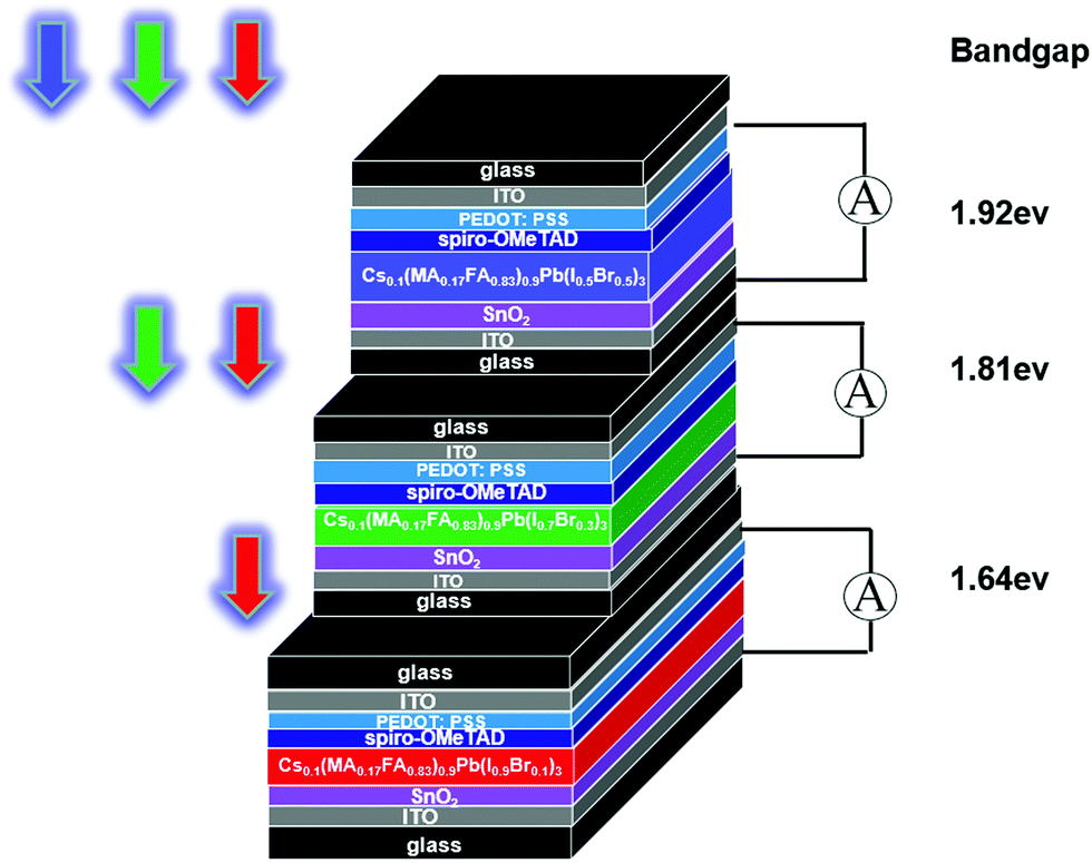 | ||
| Fig. 1 The schematic picture of the proposed perovskite multi-color detector. | ||
2. Experimental
2.1. SPSD assembly
First, triple-cation perovskite photodetectors (TCPPs) were fabricated via thin film techniques. Indium tin oxide (ITO) coated glass (20 × 20 mm2, 8 Ω, NOZO, China) was used as the top electrode and first cleaned with acetone, ethyl alcohol, and deionized water sequentially. After drying under nitrogen flow, the ITO glass was treated with UV-ozone for 15 min followed by immediately depositing the SnO2 film on the ITO side via spin-coating an aqueous SnO2 suspension at 3000 rpm for 30 s. The film was then dried at 150 °C for 30 min. The raw aqueous SnO2 suspension was obtained from Alfa and diluted with deionized water with a volume ratio of 1![[thin space (1/6-em)]](https://www.rsc.org/images/entities/char_2009.gif) :3 and stirred for 1 hour. Before spin-coating, the suspension was further filtered with a 0.22 μm-pore membrane to remove clusters.
:3 and stirred for 1 hour. Before spin-coating, the suspension was further filtered with a 0.22 μm-pore membrane to remove clusters.
For the perovskite film, a precursor solution I was prepared by mixing N,N-dimethylformamide (DMF) and dimethyl sulfoxide (DMSO) (volume ratio of 4:1), and dissolving FABr, MABr, PbBr2, and PbI2 (Sigma-Aldrich, 99.9%) salts. The molar ratios of these salts were adjusted to form type A, B, and C photodetectors, respectively, as listed in Table 1. Solution II was prepared by dissolving CsI (Sigma-Aldrich, 99.9%) in DMSO at a concentration of 1.5 M. Then 88.9 μL of solution II was mixed with 929 μL of solution I and stirred for 6 hours at room temperature in a glove box to obtain the perovskite precursor solution. The perovskite precursor solution was then spin-coated on top of the SnO2 film at 500 rpm for 10 s, followed by 6000 rpm for 25 s. Specifically, 200 μL of chlorobenzene (Sigma-Aldrich, 99.9%) was dropped evenly over the spinning substrate during the last 3 s. The substrate was then heated at 120 °C on a hot-plate for 30 min.
| Type | FAI (mM) | FABr (mM) | MABr (mM) | PbI2 (mM) | PbBr2 (mM) | |
|---|---|---|---|---|---|---|
| A | Cs0.1(MA0.17FA0.83)0.9Pb(I0.5Br0.5)3 | 0 | 1 | 0.2 | 0.38 | 0.92 |
| B | Cs0.1(MA0.17FA0.83)0.9Pb(I0.7Br0.3)3 | 0 | 1 | 0.2 | 0 | 1.3 |
| C | Cs0.1(MA0.17FA0.83)0.9Pb(I0.9Br0.1)3 | 1 | 0 | 0.2 | 1.2 | 0.1 |
The hole transport layer (HTL, the spiro-OMeTAD layer in Fig. 1) solution was formed by dissolving 72.3 mg of 2,2′,7,7′-tetrakis (N,N-di-p-methoxyphenylamine)-9,9′- spirobifluorene (spiro-OMeTAD) (Lumtec, Taiwan), 28.8 μL of ter-butylpyridine (TBP) (Sinopharm Group Co., USA) and 17.5 μL of lithium bis-(trifluoromethanesulfonyl)imide (520 mg mL−1 in acetonitrile) in 1 mL of chlorobenzene, which was then stirred for 6 h in a glove box. Then 40 μL of the prepared HTL solution was spin-casted on top of the perovskite layer at 3000 rpm for 30 s.
We then applied a piece of ITO glass as the counter electrode. A bonding layer was necessary to form strong adhesion between the spiro-OMeTAD layer and the ITO counter electrode. The bonding layer solution was first prepared by dissolving 400 mg of D-sorbitol (Heowns Inc. China) in 1 mL of poly(3,4-ethylenedioxythiophene):poly (styrene sulfonate) (PEDOT:PSS) (solid content 4%, Macklin, China). The solution was then stirred overnight and filtered through a membrane with a pore size of 5 μm. The clean ITO glass was coated with this bonding layer immediately after being treated with UV-ozone for 15 min. For the spin-coating, 100 μL of the solution was dropped on the ITO side and rotated at 1000 rpm for 30 s. After annealing at 120 °C for 10 min, the coated ITO glass was put over the HTL layer with the bonding layer facing the spiro-OMeTAD layer and laminated to form the TCPP device.
SPSDs were fabricated by stacking three TCPP devices of different perovskite formulas (Type A, B, and C as listed in Table 1) together in the order of A–B–C. The edges of the superimposed device were glued with epoxy adhesive (9005, Leaf Top, China) to realize mechanical connection and fine sealing.
2.2. Characterization
The crystal phases of the prepared perovskite films and their optical properties were investigated with an X-ray diffractometer (Rigaku Ultima-IV) and a UV–Vis absorption spectrometer (Shimadzu UV-25508, Japan), respectively.The spectral responsivity (R) and external quantum efficiency (EQE) of TCPP and SPSD devices were investigated using a spectral responsivity and external quantum efficiency measurement system (SCS100, China) and a semiconductor parameter analyzer (Keithley 4200-SCS, USA). Light-emitting diodes (LED, e-bita, China) with different central wavelengths of 630, 700 or 760 nm were used as light sources to evaluate the multi-color sensibility of the SPSD, while the incident power of the LEDs was measured with an optical power meter (Yokogawa TB200, Japan).
2.3. Detection of multi-color fluorescence QDs
Three types of CdTe QDs (Xingzi, China) with fluorescence wavelengths of 650 nm, 690 nm, and 777 nm, respectively were dissolved in water at different concentrations. For each concentration of each type of QD, 100 μL of aqueous solution was dropped on a plastic carrier. The plastic carrier was placed under the SPSD with an optical filter (HS, China, cut-off wavelength 450 nm) covering the SPSD top to block the excitation wavelength. The solution was then excited using a LED with the central wavelength at 300 nm (Ruibao, China) and the output photocurrent from the SPSD was measured using a semiconductor parameter analyzer (4200-SCS, Keithley, USA). Afterward the measured photocurrents were plotted against different concentrations of each QD solution to produce calibration curves.Also the three types of QDs with preset concentrations were mixed in one aqueous solution. The photocurrent of each TCPP stacked in the SPSD system was recorded following the same procedure mentioned above and the concentration of a certain type of QD was calculated according to its calibration curve. This concentration was then compared with the preset concentration to verify the feasibility of quantitative analysis of the SPSD.
3. Results and discussion
3.1 XRD and UV–vis absorption spectra of TCPPs
Fig. 2(a) shows the X-ray diffraction (XRD) spectra of Type A, B, and C perovskite films scanned in the range of 2θ = 20–30°. Three characteristic peaks at 20.3°, 24.8°, and 28.7° are observed in the Type C film (x = 0.1 for Br content) corresponding to (200), (202), and (220) diffraction peaks, respectively. All these three peaks shift towards higher values with the increasing Br content. With more iodine atoms replaced by smaller Br atoms (i.e., larger x), the lattice constant was reduced. Perovskite gradually transformed from an unstable tetragonal structure into a stable cubic structure, resulting in larger X-ray diffraction angles. The structural change is expected to increase the bandgaps and a blue shift of the cut-off wavelength for the photoelectric response.48 This hypothesis was confirmed with the UV-visible transmittance spectra. As shown in Fig. 2(b), the corresponding cut-off wavelength, λ, was determined by extending the linear part of a transmittance curve to the X-axis and finding the intercept. The cut-off wavelengths were identified as 645, 685, and 756 nm for Types A, B, and C, respectively. Accordingly, the bandgaps of the three perovskite film-based TCPPs (Types A, B, and C) were 1.92, 1.81, and 1.64 eV, respectively given by Eg = 1240/λ.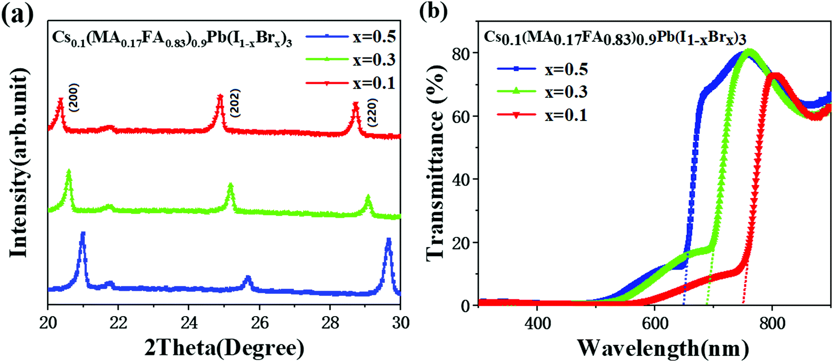 | ||
| Fig. 2 (a) XRD patterns of Cs0.1(MA0.17FA0.83)0.9Pb(I1−xBrx)3, (x = 0.5, 0.3, 0.1) magnified in the region of 2θ = 20–30°. (b) UV–vis absorption spectra of ITO/SnO2/Cs0.1(MA0.17FA0.83)0.9Pb(I1−xBrx)3, (x = 0.5, 0.3, and 0.1). | ||
3.2 Photoelectric response of TCPPs
In the case of SPSDs, the short-wavelength component of the incident light should be absorbed as completely as possible when passing through the top perovskite film-based TCPP devices and contribute as little as possible to the photoelectric response of the underneath devices. The thickness of the perovskite film in each TCPP is critical to determine how much incident light can be absorbed within a specific wavelength range.Therefore, the thickness of the three perovskite films was optimized by adjusting their spin-coating rates. The three perovskite film-based TCPPs (Types A, B, and C) were deposited at different spin-coating rates (500, 650, 800, and 1000 rpm). The scanning electron microscopy (SEM) pictures of the top view and cross-section of the three TCPPs are shown in Fig. S1(a)–(l) (ESI†). With a decrease of the spin-coating rates, the surface morphology of perovskite films did not show significant change and the thickness of the three kinds of perovskite films increases gradually. As shown in Fig. S1(m) (ESI†), the thickness showed a negative linear correlation with the spin-coating rate with a coefficient better than 0.9. The UV–vis transmittance spectra of the three TCPPs (Types A, B, and C) prepared with different spin-coating rates are shown in Fig. S1(n)–(p) (ESI†). The results suggested that the short-wavelength bands’ transmittance was reduced to approximately zero when the spin-coating rate decreased to 500 rpm. Accordingly, spin-coating at 500 rpm was employed to deposit perovskite films for the three types of TCPPs.
Moreover, the photoelectric responses of TCPPs with Type A, B, and C perovskite films under LED illumination at central wavelengths of 630 nm, 700 nm, and 760 nm, respectively, are given in Fig. S2 (ESI†). It shows that the photocurrents of the three types of TCPPs were increased by approximately four orders of magnitude compared with the dark current at the zero bias.
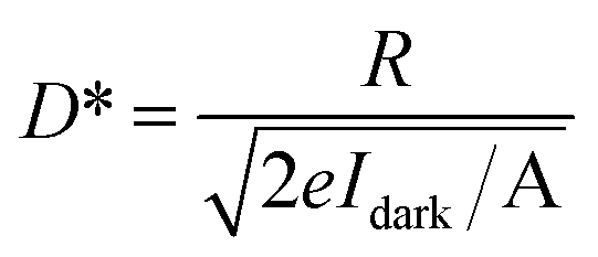
Combined with the dark current and the spectral responsivity R, the detectivity D* can be calculated according to:
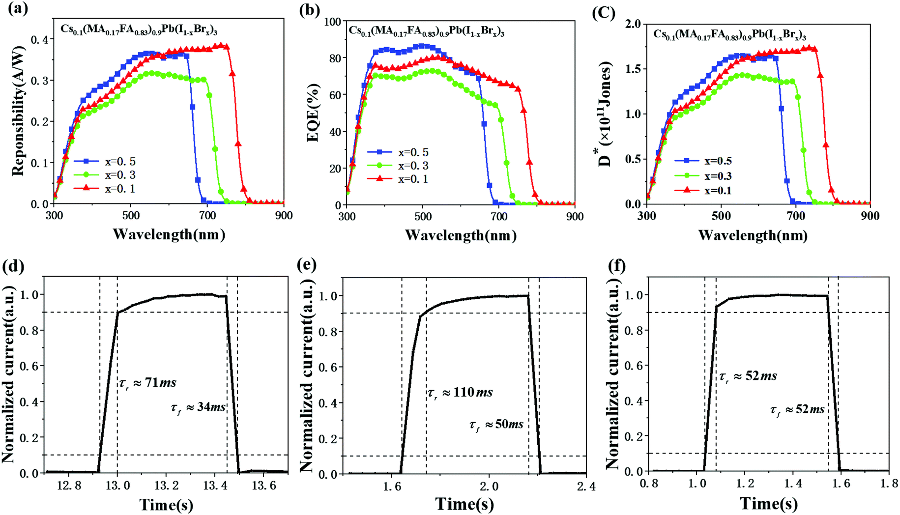 | ||
| Fig. 3 (a) Spectral response, (b) external quantum efficiency (EQE) and (c) detectivity (D*) of Cs0.1(MA0.17FA0.83)0.9Pb(I1−xBrx)3 (x = 0.5, 0.3, 0.1) TCPPs. The rise and fall time of (d) the Cs0.1(MA0.17FA0.83)0.9Pb(I0.5Br0.5)3 TCPP under 630 nm light illumination, (e) the Cs0.1(MA0.17FA0.83)0.9Pb(I0.7Br0.3)3 TCPP under 700 nm light illumination and (f) the Cs0.1(MA0.17FA0.83)0.9Pb(I0.9Br0.1)3 TCPP under 760 nm light illumination. | ||
Here the maximum spectral responses of the three TCPPs are similar, but with different response wavelength ranges. This is due to the different band gaps of the three kinds of perovskites. Therefore, the three laminated TCPPs can be used to realize segmented spectral detection.
In addition, the rise time (τr) and the fall time (τf), defined as the time required for the photocurrent to rise from 10% to 90% of its peak value and fall from 90% to 10% of the peak, are shown in Fig. 3(d–f). The rise/fall time of Type A TCPP was 71/34 ms under 630 nm (45 μw cm−2) illumination (Fig. 3(d)). The rise/fall time of Type B TCPP was 110/50 ms under 700 nm (45 μw cm−2) illumination (Fig. 3(e)). For the Type C TCPP, it was 52/52 ms under 760 nm (150 μw cm−2) illumination (Fig. 3(f)).
The comparison of TCPP devices with recently reported perovskite photodetectors is listed in Table 2. The responsivity and detection capability of TCPPs are comparable to the corresponding values of the outstanding perovskite-based photodetectors.
| Materials | Response wavelength range (nm) | EQE (%) | R (AW−1) | D* (Jones) | τ r/τf | Ref. |
|---|---|---|---|---|---|---|
| Graphene/CsPbBr3−xIx nanocrystals | 400–700 | — | 8.2 × 10⁸ | 2.4 × 10¹⁶ | 0.81/3.65 s | 49 |
| FA1−xCsxPbI3 thin films (lateral) | 240–750 | — | 5.7 | 2.7 × 10¹³ | 45/91 ns | 50 |
| CsBi3I10 thin films (lateral) | 400–800 | 4.13 × 10³ | 21.8 | 1.93 × 10¹³ | 0.33/0.38 ms | 51 |
| MAPbI3 thin films | 400–800 | 4.1 × 10⁴ | 219 | 3.1 × 10¹² | — | 52 |
| SnO2/Cs0.1(MA0.17FA0.83)0.9Pb(I0.5Br0.5)3/Spiro-OMeTAD/PEDOT:PSS | 300–680 | 86 | 0.36 | 1.75 × 10¹¹ | 71/34 ms | This work |
| SnO2/Cs0.1(MA0.17FA0.83)0.9Pb(I0.7Br0.3)3/Spiro-OMeTAD/PEDOT:PSS | 300–740 | 73 | 0.31 | 1.5 × 10¹¹ | 110/50 ms | This work |
| SnO2/Cs0.1(MA0.17FA0.83)0.9Pb(I0.9Br0.1)3/Spiro-OMeTAD/PEDOT:PSS | 300–820 | 80 | 0.38 | 1.8 × 10¹¹ | 52/52 ms | This work |
| TiO2/graphene/MAPbI3 | 260–900 | 83 | 0.375 | 4.5 × 10¹¹ | 5 ms/– | 53 |
| CsPbI3 nanowire array CVD | 300–700 | 17 | 0.0067 | 1.57 × 10⁸ | 0.292/0.234 s | 54 |
| ZnO/MAPbI3 nanowires (lateral) | 300–760 | 1300 | 4 | 1.74 × 10⁹ | 0.43/0.63 s | 55 |
3.3 Photoelectric response of a SPSD
The three types of TCPPs were piled together to form a laminar SPSD, as shown in Fig. 4(a) and 1. The photograph confirms the SPSD's compact size. Its spectral responsivity R, EQE, and detection D* were measured and are given in Fig. 4(b–d). The top layer, Type A TCPP, showed the same properties as its isolated state as summarized in Fig. 3. At the same time, the optical responses of the middle and bottom layer TCPPs changed drastically. The spectra of the middle Type B TCPP narrowed from the original 300–750 nm to 650–750 nm, with a central wavelength at 687 nm. This means that most of the light between 300 and 650 nm has been absorbed by the Type A TCPP at the top. Similarly, the spectral response of the bottom Type C TCPP changed from the original 300–800 nm to 690–800 nm, with the central wavelength at 744 nm. For the middle Type B TCPP, its maximum responsivity was 0.16 A W−1, and the full width at half maximum (FWHM) of its spectral response was 58 nm. The maximum EQE value was 30%, and the maximum D* was calculated to be 0.74 × 10¹¹ Jones. For the bottom Type C TCPP, the FWHM of its spectral response was 60 nm. The maximum responsivity and the maximum EQE value were 0.104 A W−1 and 17.4%, respectively. The maximum D* was 0.36 × 10¹¹ Jones. | ||
| Fig. 4 (a) The optical images of the SPSD. (b) Spectral responses, (c) external quantum efficiency (EQE), and (d) detectivity (D*) of the top Type A TCPP, the middle Type B TCPP, and the bottom Type C TCPP of the SPSD, respectively. | ||
With the central wavelength positions distinctly separated, the 3-layer SPSD is expected to have multi-color recognition capabilities. It was then evaluated using LEDs of different central wavelengths as the light sources. Three LEDs with central wavelengths at 630, 700, and 760 nm were turned on in sequences. The time-dependent input optical power density and the induced photocurrent of the SPSD were recorded. The results shown in Fig. S3 (ESI)† indicate that each TPCC layer could sense wavelengths better fitting its perovskite film's bandgap and corresponding to the central wavelengths mentioned in Fig. 4. The experimental results clearly show that the SPSD is able to detect light sources of different wavelengths simultaneously.
The as-fabricated SPSDs were stored at 25 °C and at a relative humidity of 50% for 10, 20, and 30 days. Fig. S4(a–c) (ESI†) show the photocurrents of the SPSD after storing for 10, 20, and 30 days, respectively. The same LED light sources and optical intensities were employed as those used in Fig. S2 (ESI†) and Fig. 3, i.e., 630 nm (45 μW cm−2), 700 nm (45 μW cm−2), and 760 nm (150 μW cm−2). As a result, the SPSD did not show significant degradation even after 30-day storage. Again, the SPSD samples were tested at 50 °C and at a relative humidity of 50% for 500 hours and the result is shown in Fig. S4(d) (ESI†). It can be seen that the photocurrent of the SPSD does not decrease significantly, which indicates the good thermal and long-term stability of the SPSD.
The SPSD samples were tested at various temperatures from 5 °C to 70 °C with a step of 5 °C, and the stability time at each temperature is 20 minutes and the relative humidity remained at 50%. The result is shown in Fig. S4(e) (ESI†). Accordingly, the photocurrent of the SPSD does not change abruptly with the varied temperature.
3.4 Multi-color fluorescence detection
The simultaneous detection of three kinds of fluorescent CdTe QDs by the SPSD was implemented. To our best knowledge, this is the first time a quantitative analysis of multiple QDs using one detector without optical dispersive devices or filters has been performed.The morphology and optical properties of the three kinds of CdTe QDs were examined. Fig. S5(a–c) (ESI†) show the transmission electron microscopy (TEM) images of the QDs with particle sizes ranging from 3 to 8 nm. Fig S5d (ESI†) shows the photoluminescence (PL) spectra of the three kinds of QDs. The emission peak positions of the three QDs were at 650, 690, and 777 nm, respectively. The intensity of the emission peak of the three QDs under 300 nm excitation light was different. The intensity of the QDs with the emission peak of 690 nm was larger than those of the other two kinds of QDs, resulting in a higher photocurrent of the Type B TCPP than the other two TCPP layers.
Fig. 5 shows the measurement setup and the calibration curves. The SPSD exhibited linear relationships between the photocurrents and the QD concentrations for the three kinds of QDs with correlation coefficients all better than 0.99. The LOD of the QD at 650 nm was 6.16 nM based on the 3n rule. The LOD can be calculated based on the equation LOD = (3σ/K), where σ is the standard deviation of the blank signal, and K is the slope of the calibration curve.56 In the same way, the LOD of the QD at 690 nm was 8.11 nM, and the LOD of the QD at 777 nm was 7.25 nM.
 | ||
| Fig. 5 (a) The test apparatus, and (b) the photocurrent-concentration calibration curves for aqueous solutions of three kinds of QDs with central wavelengths at 650 nm, 690 nm, and 777 nm, respectively. | ||
The three kinds of QDs with preset concentrations were then mixed to evaluate the feasibility of quantitative measurements by the SPSD. Two aqueous solutions with different preset concentrations within the range of 10 to 50 nM were dropped on a solution carrier and excited with the UVLED light, and the photocurrent of each TCPP layer of the SPSD system was recorded. The concentration of each QD type could be deduced by substituting the measured photocurrent into the corresponding calibration curve as shown in Fig. 5a. As shown in Table 3, the calculated results match the preset concentrations by a deviation less than 20%.
| Group 1 | Group 2 | |||||
|---|---|---|---|---|---|---|
| QD wavelength (nm) | 650 | 690 | 777 | 650 | 690 | 777 |
| Preset concentration (nM) | 50 | 10 | 30 | 35 | 20 | 50 |
| Derived concentration (nM) | 56.5 | 12 | 35.5 | 37 | 21.2 | 56 |
| Relative deviation (%) | 13 | 20 | 18.3 | 5.7 | 6.25 | 12 |
| Relative standard deviation (RSD) (%) | 4.1 | 3.7 | 5.4 | 3.3 | 3.9 | 5.1 |
The LOD of the three kinds of CdTe QDs is 6.16, 7.25 and 8.11 nM, respectively, which can meet the requirement for most fluorescence analysis applications.57,58 The deviation of up to 20% is possibly due to defects at the interfaces between different materials in the thin film-structured detectors that induce leakage currents as well as background noise. In future work, the performance of SPSDs could be further improved by passivating the interface defects.
4. Conclusions
Three triple-cation perovskite photodetectors with different bandgaps were successfully fabricated by adjusting the composition of halogen elements in the perovskite thin films, which were stacked to form an SPSD. The thickness of the perovskite film of the three photodetectors in the SPSD was optimized by tuning the spin-coating process to detect the incident light better. The SPSD showed good thermal and long-term stability in air. Moreover, fluorescent CdTe QDs of different central wavelengths (650 nm, 690 nm, and 777 nm, respectively) in a mixed solution were quantitatively detected by the SPSD. The LOD of the three CdTe QDs was calculated to be 6.16, 7.25, and 8.11 nM, respectively. In future work, SPSDs stacked with more layers are promising to increase the multi-color detection ability, and SPSDs can be miniaturized and arranged in an array to realize multi-color imaging.Author contributions
This manuscript was written through contributions from all authors. M. L. supervised this work; K. Z. performed the experiments and analysis and prepared the original draft. X. L. and L. K. Y. guided perovskite preparation. X. L., J. Q. C. and X. Y. C provided specifically critical review, commentary and revision; J. Q. W. prepared the QD solution.Conflicts of interest
There are no conflicts to declare.Acknowledgements
This work was supported by the NSFC under the project No. 62174142 and NSFC under the project No. 62175204.References
- K. J. Baeg, M. Binda, D. Natali, M. Caironi and Y. Y. Noh, Adv. Mater., 2013, 25, 4267–4295 CrossRef CAS PubMed.
- G. Konstantatos and E. H. Sargent, Nat. Nanotechnol., 2010, 5, 391–400 CrossRef CAS.
- L. P. Schuler, J. S. Milne, J. M. Dell and L. Faraone, J. Phys. D: Appl. Phys., 2009, 42, 133001 CrossRef.
- M. A. Druy, R. A. Crocombe, J. Malinen, A. Rissanen, H. Saari, P. Karioja, M. Karppinen, T. Aalto and K. Tukkiniemi, Proc. SPIE, 2014, 9101, 91010C Search PubMed.
- W. Piyawattanametha, Y.-H. Park, M. Ebermann, N. Neumann, K. Hiller, M. Seifert, M. Meinig and S. Kurth, Proc. SPIE, 2016, 9760, 97600H CrossRef.
- R. A. Crocombe, Appl. Spectrosc., 2018, 72, 1701–1751 CrossRef CAS.
- P. Edwards, C. Zhang, B. Zhang, X. Hong, V. K. Nagarajan, B. Yu and Z. Liu, Sci. Rep., 2017, 7, 12224 CrossRef PubMed.
- P. J. Lapray, X. Wang, J. B. Thomas and P. Gouton, Sensors, 2014, 14, 21626–21659 CrossRef PubMed.
- T. Skauli, H. E. Torkildsen, S. Nicolas, T. Opsahl, T. Haavardsholm, I. Kasen and A. Rognmo, Appl. Opt., 2014, 53, C64–C71 CrossRef.
- M. A. Martinez, E. M. Valero, J. Hernandez-Andres, J. Romero and G. Langfelder, Appl. Opt., 2014, 53, C14–C24 CrossRef PubMed.
- Y. Murakami, M. Yamaguchi and N. Ohyama, Opt. Express, 2012, 20, 7173–7183 CrossRef.
- S. Nishiwaki, T. Nakamura, M. Hiramoto, T. Fujii and M.-A. Suzuki, Nat. Photonics, 2013, 7, 240–246 CrossRef.
- R. B. Merrill, US Pat., US005965875A, 1999 Search PubMed.
- R. F. Lyon and P. M. Hubel, Soc. Imaging Sci. Technol., 2002, 1, 349–355 Search PubMed.
- J. A. Theil, M. Cao, G. Kooi, G. W. Ray, W. Greene, J. Lin, A. Budrys and U. Yoon, MRS Online Proc. Libr., 1999, 609, 1431–1436 Search PubMed.
- R. D. Jansen-van Vuuren, A. Armin, A. K. Pandey, P. L. Burn and P. Meredith, Adv. Mater., 2016, 28, 4766–4802 CrossRef CAS PubMed.
- M. Topic, H. Stiebig, D. Knipp and F. Smole, IEEE Trans. Electron Devices, 1999, 46, 1839–1845 CrossRef CAS.
- P. M. Hubel, Soc. Imaging Sci. Technol., 2005, 1, 314–317 Search PubMed.
- M. M. Blouke, P. M. Hubel, N. Sampat, J. Liu, R. J. Guttosch and R. J. Motta, Sens. Camera Syst. Scienti. Indust. Digit. Photogr. Appli. V, 2004, 5301, 402–407 Search PubMed.
- N. Pellet, P. Gao, G. Gregori, T. Y. Yang, M. K. Nazeeruddin, J. Maier and M. Gratzel, Angew. Chem., Int. Ed., 2014, 53, 3151–3157 CrossRef CAS.
- J. H. Noh, S. H. Im, J. H. Heo, T. N. Mandal and S. I. Seok, Nano Lett., 2013, 13, 1764–1769 CrossRef CAS PubMed.
- R. Dong, Y. Fang, J. Chae, J. Dai, Z. Xiao, Q. Dong, Y. Yuan, A. Centrone, X. C. Zeng and J. Huang, Adv. Mater., 2015, 27, 1912–1918 CrossRef CAS.
- Z. Lian, Q. Yan, Q. Lv, Y. Wang, L. Liu, L. Zhang, S. Pan, Q. Li, L. Wang and J. L. Sun, Sci. Rep., 2015, 5, 16563 CrossRef.
- D. N. Dirin, I. Cherniukh, S. Yakunin, Y. Shynkarenko and M. V. Kovalenko, Chem. Mater., 2016, 28, 8470–8474 CrossRef CAS.
- G. Xing, N. Mathews, S. Sun, S. S. Lim, Y. M. Lam, M. Grätzel, S. Mhaisalkar and T. C. Sum, Science, 2013, 342, 344–347 CrossRef CAS PubMed.
- K. Domanski, W. Tress, T. Moehl, M. Saliba, M. K. Nazeeruddin and M. Grätzel, Adv. Funct. Mater., 2015, 25, 6936–6947 CrossRef CAS.
- S. Yakunin, Y. Shynkarenko, D. N. Dirin, I. Cherniukh and M. V. Kovalenko, NPG Asia Mater., 2017, 9, e431 CrossRef CAS.
- W. Qarony, M. Kozawa, H. A. Khan, M. I. Hossain, A. Salleo, Y. H. Tsang, J. Y. Hardeberg, H. Fujiwara and D. Knipp, Adv. Mater. Interfaces, 2020, 7(17), 2000459 CrossRef CAS.
- M. I. Hossain, H. A. Khan, M. Kozawa, W. Qarony, A. Salleo, J. Y. Hardeberg, H. Fujiwara, Y. H. Tsang and D. Knipp, ACS Appl. Mater. Interfaces, 2020, 12, 47831–47839 CrossRef CAS PubMed.
- R. E. Burton, E. J. White, T. R. Foss, K. M. Phillips, R. H. Meltzer, N. Kojanian, L. W. Kwok, A. Lim, N. L. Pellerin, N. V. Mamaeva and R. Gilmanshin, Lab Chip, 2010, 10, 843–851 RSC.
- Z. Liu, X. Yang, Y. Zhang, Y. Zhang, Z. Zhu, X. Yang, J. Zhang, J. Yang and L. Yuan, Sens. Actuators, B, 2018, 265, 211–216 CrossRef CAS.
- J. Chou, J. Wong, N. Christodoulides, P. N. Floriano, X. Sanchez and J. McDevitt, Sensors, 2012, 12, 15467–15499 CrossRef.
- P. Sabhachandani, N. Cohen, S. Sarkar and T. Konry, Microchim. Acta, 2015, 182, 1835–1840 CrossRef CAS.
- T. Anazawa and M. Yamazaki, Lab Chip, 2017, 17, 4231–4242 RSC.
- Z. Hu, A. Glidle, C. N. Ironside, M. Sorel, M. J. Strain, J. Cooper and H. Yin, Lab Chip, 2012, 12, 2850–2857 RSC.
- R. Halir, L. Zavargo-Peche, D. X. Xu, P. Cheben, R. Ma, J. H. Schmid, S. Janz, A. Densmore, A. Ortega-Moñux, Í. Molina-Fernández, M. Fournier and J. M. Fédeli, Opt. Quantum Electron., 2012, 44, 521–526 CrossRef CAS.
- Z. Hu, A. Glidle, C. Ironside, J. M. Cooper and H. Yin, Lab Chip, 2015, 15, 283–289 RSC.
- M. Saliba, T. Matsui, K. Domanski, J.-Y. Seo, A. Ummadisingu, S. M. Zakeeruddin, J.-P. Correa-Baena, W. R. Tress, A. Abate and A. Hagfeldt, Science, 2016, 354, 206–209 CrossRef CAS PubMed.
- M. Salado, M. A. Fernandez, J. P. Holgado, S. Kazim, M. K. Nazeeruddin, P. J. Dyson and S. Ahmad, ChemSusChem, 2017, 10, 3846–3853 CrossRef CAS.
- M. Stolterfoht, C. M. Wolff, Y. Amir, A. Paulke, L. Perdigón-Toro, P. Caprioglio and D. Neher, Energy Environ. Sci., 2017, 10, 1530–1539 RSC.
- Y. Wang, J. Wu, P. Zhang, D. Liu, T. Zhang, L. Ji, X. Gu, Z. David Chen and S. Li, Nano Energy, 2017, 39, 616–625 CrossRef CAS.
- T. Zhang, J. Wu, P. Zhang, W. Ahmad, Y. Wang, M. Alqahtani, H. Chen, C. Gao, Z. D. Chen, Z. Wang and S. Li, Adv. Opt. Mater., 2018, 6, 1701341 CrossRef.
- S. Chu, H. Wang, X. Ling, S. Yu, L. Yang and C. Jiang, ACS Appl. Mater. Interfaces, 2020, 12, 12962–12971 CrossRef CAS PubMed.
- R. Jiang, Y. Zhang, Q. Zhang, L. Li and L. Yang, ACS Appl. Nano Mater., 2021, 4, 9760–9767 CrossRef CAS.
- H. Wang, L. Yang, S. Chu, B. Liu, Q. Zhang, L. Zou, S. Yu and C. Jiang, Anal. Chem., 2019, 91, 9292–9299 CrossRef CAS.
- S. Han, L. Yang, Z. Wen, S. Chu, M. Wang, Z. Wang and C. Jiang, J. Hazard. Mater., 2020, 398, 122894 CrossRef CAS PubMed.
- X. N. Zhu, Y. K. Zhang, Y. Q. Zhang, Z. Q. Yan, C. C. Nie, X. J. Lyu, Y. J. Tao, J. Qiu and L. Li, J. Hazard. Mater., 2020, 392, 122322 CrossRef CAS PubMed.
- Y. Zhang, Y. Liu, Y. Li, Z. Yang and S. Liu, J. Mater. Chem. C, 2016, 4, 9172–9178 RSC.
- D.-H. Kwak, D.-H. Lim, H.-S. Ra, P. Ramasamy and J.-S. Lee, RSC Adv., 2016, 6, 65252–65256 RSC.
- F.-X. Liang, J.-Z. Wang, Z.-X. Zhang, Y.-Y. Wang, Y. Gao and L.-B. Luo, Adv. Opt. Mater., 2017, 5(22), 1700654 CrossRef.
- X. W. Tong, W. Y. Kong, Y. Y. Wang, J. M. Zhu, L. B. Luo and Z. H. Wang, ACS Appl. Mater. Interfaces, 2017, 9, 18977–18985 CrossRef CAS.
- W. Hu, R. Wu, S. Yang, P. Fan, J. Yang and A. Pan, J. Phys. D: Appl. Phys., 2017, 50, 375101 CrossRef.
- J. Li, S. Yuan, G. Tang, G. Li, D. Liu, J. Li, X. Hu, Y. Liu, J. Li, Z. Yang, S. F. Liu, Z. Liu, F. Gao and F. Yan, ACS Appl. Mater. Interfaces, 2017, 9, 42779–42787 CrossRef CAS PubMed.
- A. Waleed, M. M. Tavakoli, L. Gu, S. Hussain, D. Zhang, S. Poddar, Z. Wang, R. Zhang and Z. Fan, Nano Lett., 2017, 17, 4951–4957 CrossRef CAS.
- T. Gao, Q. Zhang, J. Chen, X. Xiong and T. Zhai, Adv. Opt. Mater., 2017, 5, 1700206 CrossRef.
- N. B. Brahim, N. B. H. Mohamed, M. Echabaane, M. Haouari, R. B. Chaâbane, M. Negrerie and H. B. Ouada, Sens. Actuators, B, 2015, 220, 1346–1353 CrossRef.
- S. N. Wang, J. Zhu, X. Li, J. J. Li and J. W. Zhao, Spectrochim. Acta, Part A, 2018, 201, 119–127 CrossRef CAS.
- H. Xu, R. Miao, Z. Fang and X. Zhong, Anal. Chim. Acta, 2011, 687, 82–88 CrossRef CAS.
Footnote |
| † Electronic supplementary information (ESI) available: See DOI: 10.1039/d1tc04489c |
| This journal is © The Royal Society of Chemistry 2022 |