Controllable spin direction in nonmagnetic BX/MX2 (M = Mo or W; X = S, Se and Te) van der Waals heterostructures by switching between the Rashba splitting and valley polarization†
Dongxue
Zhang
and
Baozeng
Zhou
 *
*
Tianjin Key Laboratory of Film Electronic & Communicate Devices, School of Integrated Circuit Science and Engineering, Tianjin University of Technology, Tianjin 300384, China. E-mail: baozeng@tju.edu.cn
First published on 25th November 2021
Abstract
Manipulating the physical properties using the spin degree of freedom constitutes a major part of modern condensed matter physics and is a key aspect of spintronic devices. Using density functional theory calculations, we predict that the spin direction can be controlled in nonmagnetic BX/MX2 (M = Mo or W; X = S, Se and Te) van der Waals heterostructures. The stability of the heterostructures is confirmed by calculating their binding energies and phonon dispersion plots. The electronic structures of the heterostructures demonstrate that all of them maintain the semiconducting nature, but have different band alignment, which is related to orbital components at the band-edge and influenced by electron transfer at the interface. By considering the spin–orbit coupling, the Rashba-type spin splitting with the in-plane spin and valley polarization with the out-of-plane spin can be formed and coexist at the valence-bands of BSe/MoSe2 and BSe/WSe2. Moreover, the dominant carrier spin direction around the valence-band edge can be effectively tuned by exerting a biaxial strain and external electrical field. These calculations show that manipulation of the spin within semiconductor devices to exploit the full potential of materials with a gap for charge control without the use of auxiliary ferromagnetic materials and magnetic fields can be achieved in the newly discovered two-dimensional van der Waals system.
Introduction
Due to their unique physical and electrical properties, two-dimensional (2D) transition–metal dichalcogenides (TMDs), such as MoS2, MoTe2, and WSe2, have been attracting tremendous research interest in recent years.1–4 Due to the interaction of the thin layers in the various bulk compounds, they can be manufactured by mechanical exfoliation.5,6 The band splitting appears at the K and K′ valleys arising from the absence of inversion symmetry in the H phase,7,8 which is crucial for the manipulation and utilization of the valley degree of freedom in the valleytronics field.9,10 After theoretically proposing the concept of the valley polarization by circularly polarized light, it was implemented by several experimental groups.11,12 Moreover, some strategies have been developed to widen the applicability of TMDs. Forming a semiconductor interface enables the creation of the advanced characteristics and properties that are currently lacking in a single 2D material.13–16 Heterostructures formed by mechanically stacking 2D semiconducting materials with weak van der Waals (vdW) forces have been widely investigated theoretically and experimentally.17–23 Although the vdW interaction is much weaker than that of ionic and covalent bonds, it can still alter the electronic properties of a material. Thus, these vertical stacked heterostructures not only preserve the intrinsic electronic properties of single materials but also yield novel functionalities. Examples are the large exchange splitting in graphene/NiI2 by the proximity effect and the formation of type-II band alignment in InSe/WS2.24,25 Interestingly, the Rashba effect can play a decisive role in the electronic states in heterostructures and on surfaces.Generally, the Rashba effect established from strong spin–orbit coupling (SOC) with structure inversion asymmetry is a significant effect that intrinsically affects the carrier dynamics. The electron dispersion relation, E(k), is usually described by the effective-mass approximation, with a spin-degenerate parabolic dispersion
 | (1) |
 | (2) |
The search for Rashba SOC has been recently revived by 2D materials and their vdW heterostructures.37–41 In few-layer Bi2Se3/PtSe2, the Rashba splitting coexists in both conduction and valence bands.42 Recent developments in the experimental realization of 2D vdW systems also paved the way for the investigation of spin-orbitronics and the Rashba effect.43–45 Particularly, in Janus TMDs with a broken out-of-plane mirror symmetry,46–48 the Rashba-type spin splitting (in-plane spin) and band splitting at the K/K′ valleys (out-of-plane spin) are coexistent. The heterostructure allows for precise control of the desired physical properties and has helped realizing the concept of materials by design.49–51 In a 2D vdW heterostructure, different requirements pertaining to optimal Rashba bands can be dealt with one by one. Therefore, constructing TMD-based vdW heterostructures, with broken inversion symmetry, will provide a promising platform for studying spin physics. In the present work, to avoid the interference of band folding on the valley polarization (K/K′ points) and Rashba splitting (Γ point), B-based monochalcogenides,52 which have a hexagonal structure and similar lattice parameters with TMDs, are used to construct BX/MX2 (M = Mo or W; X = S, Se and Te) heterostructures. By calculating the electronic structures of the heterostructures, we demonstrate that all of them maintain their semiconducting nature, but have different band alignments, which may be related to the electron transfer at the interface. By considering the SOC, the Rashba-type spin splitting with in-plane spin and valley polarization with out-of-plane spin can be formed and coexist at the valence-band of BSe/MoSe2 and BSe/WSe2. Moreover, the dominant carrier spin direction around the valence-band edge can be effectively tuned by exerting a biaxial strain and external electrical field, providing a promising material for spin FET application.
Computational details and models
Density functional theory (DFT) calculations for structural relaxation and electronic structures are performed by using the Perdew–Burke–Ernzerhof generalized gradient approximation (PBE–GGA) for the exchange and correlation function as implemented in the Vienna ab initio simulation package (VASP).53–55 The projector augmented wave (PAW) method is used to described the electron–ion interaction.53,56 The applied energy cutoff for plane wave is 500 eV to guarantee the accuracy of calculations. The Brillouin zone is sampled with Γ-centered 12 × 12 × 1 k-point meshes. A vacuum thickness of 25 Å is used in the z direction to preclude interactions between periodic images. The convergence criteria for energy and atomic forces are 10−6 eV and 0.01 eV Å−1, respectively. The SOC is not included during the geometry optimization but is added in the electronic structure calculations. The hybrid Heyd–Scuseria–Ernzerhof (HSE06) functional is also utilized to obtain a better estimation of the electronic structures.57,58 The vdW correction is adopted by the DFT-D2 empirical dispersion of Grimme,59 and dipole corrections are also considered. To ensure the structural stability of these systems, the phonon dispersion plot is calculated using a finite displacement method on a 3 × 3 × 1 supercell with 63 atoms by using the PHONOPY package.60 The PYPROCAR code is used to calculate the constant energy contour plots of the spin texture.61The binding energy (Eb) is calculated as follows
| Eb = (EBX/MX2 − EBX − EMX2)/N, | (3) |
| Δρ = ρBX/MX2 − ρBX − ρMX2, | (4) |
Results and discussion
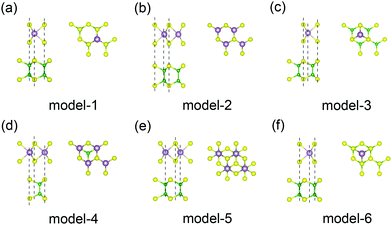
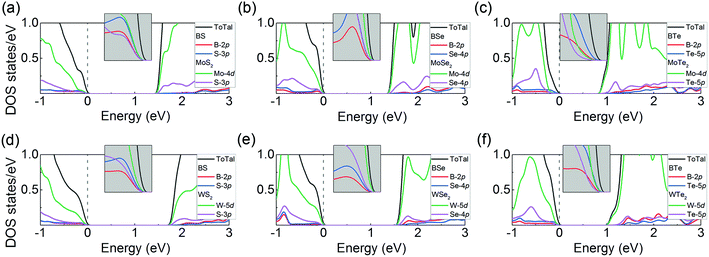
Before constructing heterostructures, first we examine the geometric and electronic band structures of pristine BX and MX2 (M = Mo or W; X = S, Se and Te) monolayers. With the same chalcogen, the lattice parameters of the components are very close to each other, resulting in a small lattice mismatch and making it easy to form stable heterostructures in the vertical direction. The obtained lattice parameters are listed in Table S1 (ESI†), which match with previous reports.52,62 As shown in Fig. S1 (ESI†), all the isolated TMDs have the direct band-gaps at the K point, decreasing with the increase of the atomic number of chalcogen. When SOC is considered, the bands split along the Γ–K–M k-path due to the absence of inversion symmetry, which will not change the direct band-gap behavior. The B-based monochalcogenides are indirect band-gap semiconductors with the conduction-band minimum (CBM) located at the M point and the valence-band resembling a Mexican hat around the Γ point. The SOC just reduces the band-gaps and will not induce significant band splitting in these systems. Then, we build the supercell model of the BX/MX2 heterostructure by attaching the primitive cells of BX and MX2 together. Due to the different stacking order of the interface atoms, six possible configurations are considered and shown in Fig. 1. Each stacking is obtained either by a monolayer translation and/or a rotation with respect to each other. In our theoretical simulation, the lattice constants of the heterostructures are first sited to the average value due to the small lattice mismatch. During atomic structure relaxation calculations to find the most energetically favorable structures, all the atoms and in-plane lattice vectors of the simulation model are free to relax. The vacuum layer of the vertical direction is fixed and reasonable interfacial spacing can be obtained by considering the vdW effect. After the binding energy calculations, model-1 is found to be the most stable configuration, in which all metal atoms (Mo, W or B) are aligned with the chalcogen atoms of the different layers. The in-plane lattice constant a, equilibrium interlayer distance di, and binding energies Eb of the heterostructures in the model-1 configuration with different component elements are shown in Table S1 (ESI†). All the energies are much lower than that of bilayer graphene (−100 meV).63 The negative value corresponds to an exothermic reaction, which further confirms their stability.64–66 We also relax different stackings of each heterostructure at one lattice parameter, and the calculated total energies are listed in Table S2 (ESI†). It can be found that among all the heterostructures, the stacking configuration model-1 still has the lowest total energy, which is consistent with the previous determination by Eb. To discuss the dynamic stability of the BX/MX2 systems, Fig. S2 (ESI†) shows that the phonon dispersions of BX/MX2 heterostructures exhibit a similar overall shape to the phonon frequencies, softening with an increase in the mass of X. The discrepancy between them is consistent with the distinctions on interlayer distance and binding energy. Moreover, the absence of imaginary frequencies in the entire Brillouin zone confirms the dynamical stability of all the heterostructures.The band structures of BX/MX2 heterostructures obtained by our calculations without SOC are shown in Fig. 2. The Fermi level is set to the valence-band maximum (VBM) in all band structures. Since the heterostructure is formed by the interlayer vdW interaction which is relatively weaker than intralayer bonding, the band structure should preserve most of the characteristics of its constituent monolayers. As expected, all heterostructures exhibit the semiconducting nature with an indirect band-gap, which decreases with the increase of the atomic mass of chalcogens. Orbital projections show that the bands around the CBM are mainly contributed by the Mo-4d or W-5d orbitals from the MX2 layer, which is confirmed by the PDOS in Fig. 3. However, the orbital distribution at the VBM is affected by the chalcogen. In BS/MoS2 (BS/WS2), there is strong hybridization between the component monolayers at the VBM around the Γ point. The hybridization orbitals mainly come from the Mo-4d (W-5d) of the MoS2 (WS2) layer and S-3p of the BS layer. In BSe/MoSe2 (BSe/WSe2), the VBM is only contributed by the Mo-4d (W-5d) orbitals of the MoS2 (WS2) layer, making the systems behave as the standard type-I band alignment. Therefore, in these systems, the BSe only provides a vertical electric field through the coupling of the vdW interface to break the inversion symmetry of the MoSe2 (WSe2) layer without affecting the orbital components around the Fermi level (VBM and CBM), which are the ideal platform for the study of valley polarization and Rashba splitting. However, upon further increasing the atomic mass of chalcogen, in BTe/MoTe2 (BTe/WTe2), Te-5p states will move close to the Fermi level due to the strong orbital delocalization, and eventually cross the Mo-4d (W-5d) orbitals, causing the heterostructures to transfer into a type-II band alignment. With such band characteristics, free electrons and holes are spontaneously separated, which is suitable for the photovoltaic effect and solar energy conversion applications. A similar phenomenon has been observed in other vdW heterostructures, such as MoS2/WS2,67 MoS2/h-BN68 and black phosphorene/MoS2.69 In Fig. S3 (ESI†), the band structures of BX/MX2 heterostructures obtained by optb86-vdW is also shown. Obviously, the influence of the optb86-vdW density functional on the band structure is almost the same as that of DFT-D2. Since PBE is known to underestimate the band-gap, we employed the HSE06 hybrid functional to predict a more reasonable energy band-gap. Fig. S4 (ESI†) shows the total DOS and orbital-resolved PDOS calculated by the HSE06 method for all heterostructures. It is worth mentioning that the HSE06 functional only enhances the band-gap without any notable changes in the orbital contributions of the VBM and CBM.
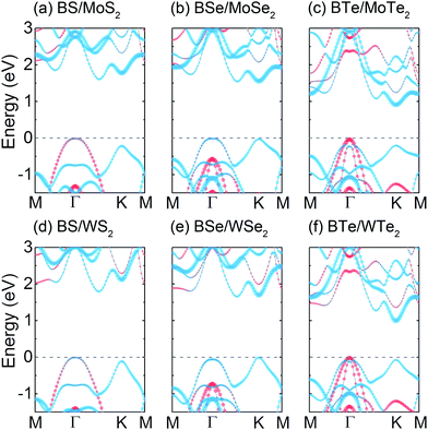 | ||
| Fig. 2 Band structures of the BX/MX2 heterostructures obtained without SOC. The size of the circles denotes the projection on BX (red) and MX2 (blue). The Fermi level is set to zero. | ||
When the SOC is considered, heterostructures retain the semiconducting behavior with indirect band-gaps, as shown in Fig. 4. Moreover, the heterostructures preserve the large spin splitting of the highest valence band at the K point with a slight reduction compared with those in monolayer TMDs. As analyzed above, with the type-I band alignment, the bands near the VBM in BSe/MoSe2 (BSe/WSe2) are mainly dominated by the MoSe2 (WSe2) layer, see Fig. 4(b) and (e). Interestingly, the Γ point exhibits an emerged spin splitting, which does not appear in monolayer MoSe2 (WSe2) (see the label area in Fig. S6, ESI†) and should be related to the interaction in the heterostructure. The morphology is similar to the Rashba splitting in Janus TMDs with broken mirror symmetry,48,70–72 suggesting that an out-of-plane polarized electric field in the 2D system is a necessary condition for the Rashba effect. In BSe/MoSe2 (BSe/WSe2), the interaction between BSe and MoSe2 (WSe2) achieves Rashba splitting, as the formation of interface dipole behavior. To confirm that the observed band splitting is the Rashba-type, Fig. 5 shows the spin texture calculated in a kx–ky plane centered at the Γ point, as labeled in Fig. 4(b) and (e). The projection of different spin components on the electronic bands manifests that the spin direction is mainly in-plane (Sx and Sy). In the Rashba-type spin splitting, the Hamiltonian can be represented as HR = aR(σxky − σykk), with σ and k denoting the Pauli matrices and in-plane momentum, respectively.73 The constant-energy cuts show outer and inner circles with clockwise and counterclockwise rotating spin directions, respectively. This pattern is consistent with the characteristics of the Rashba Hamiltonian.74 The origin of the small out-of-plane spin component (Sz) is the in-plane electric field due to inversion symmetry breaking in the heterostructures. The strength of the Rashba-type spin splitting can be characterized by the Rashba parameter aR = 2ER/kR, where ER is the energy difference between the VBM and the band crossing at the Γ point, and KR is the momentum offset, respectively, as shown in Fig. 4(b) and (e). For the BSe/MoSe2 heterostructure, we obtain ER = 8.3 meV and kR = 0.01069 Å−1, so that aR = 1.55 eV Å, while for the BSe/WSe2 heterostructure the obtained values are ER = 6.4 meV and kR = 0.0089 Å−1, so that aR = 1.44 eV Å. The magnitude of the Rashba splitting for the BSe/MoSe2 (BSe/WSe2) heterostructures is comparable to that of the previous report in PtSe2/MoSe275 and almost twice as large as those in Janus TMDs.48,71 If carriers move through these semiconducting systems, the effective SOC magnetic field will be changed suddenly due to the momentum-changing scattering, thus leading to spin randomization. A large Rashba parameter implies significant SOC interactions, desirable for suppressing the spin relaxation, controlling the spin precession, and robustness against all forms of spin-independent scattering.26,46 Thus, such huge Rashba spin splitting can be taken as a promising candidate for spin FET applications.
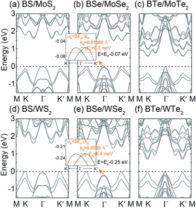 | ||
| Fig. 4 The band structures of BX/MX2 heterostructures obtained with SOC. The insets of (b) and (e) show the magnified band structures around the Γ point. | ||
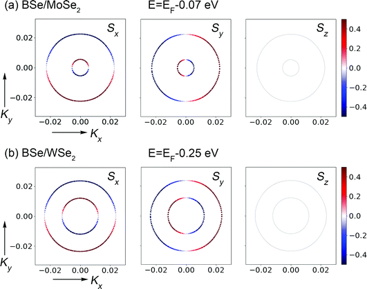 | ||
| Fig. 5 Spin texture calculated in a kx–ky plane centered at the Γ point, at an energy surface 0.07 eV (0.25 eV) below the Fermi level in (a) BSe/MoSe2 and (b) BSe/WSe2. | ||
To gain deep mechanistic insights, the planar averaged charge density differences and related electron transfer models are illustrated in Fig. S5 (ESI†). In all cases, we find that the negative charges are mainly visualized around the B-based monochalcogenide layer, whereas the TMD layer has positive charges, implying that the charges are mainly accumulated in the TMD layer, while they are depleted in the B-based monochalcogenide layer. The work functions of monolayers and their heterostructures are also calculated to explain the charge redistribution at the interfaces. The work functions of the TMD layers are all larger than those of B-based monochalcogenide layers, implying that the TMD layers acquire electrons from B-based monochalcogenide layers, and then leading to the formation of a strong inner electric field across the interface, which can be used to achieve the Rashba effect. Furthermore, we notice that when Mo is replaced by W, the Rashba splitting decreases, which is opposite to the trend of the band splitting at the K point. It is shown that there is hybridization between Mo-4d (W-5d) and Se-4p orbitals at the VBM by considering SOC. Not the d but p orbitals are responsible for the Rashba splitting, and the replacement may enhance d orbital contributions at the expense of p orbital contributions. Thus, in Fig. 4(c) and (f), the enhancement of SOC and p orbital contributions of Te at the valence-band edge around the Γ point will induce a much stronger Rashba splitting. However, with a type-II band alignment, the Rashba splitting is covered by the bands around the VBM, which inhibits its practical application.
More importantly, except for the Rashba-type spin splitting around the Γ point due to the inner electric field across the interface induced by the mirror asymmetry, SOC together with inversion symmetry breaking also gives rise to the Zeeman-type spin splitting around the corners of the 2D Brillouin zone (K/K′ valleys), as shown in Fig. S7 (ESI†). The respective time-reversal symmetry requires that the spin splitting must be opposite at the two distinct valleys with an out-of-plane spin direction (Sz), which is similar to the case of valley polarization in TMD monolayers and contributed to the valley Hall effect.76 The spin direction around the Γ point is mainly in-plane, as shown from the spin projection along Sx and Sy, which is consistent with the discussion of the spin texture in Fig. 5. However, the VBM is located at the K/K′ points for both BSe/MoSe2 and BSe/WSe2, indicating that the Rashba electronic states are inaccessible for transport. As the Fermi level is tuned to the VBM by gating or hole doping of the substrate, the in-plane electric field (E) will drive the carriers near the K/K′ points to move perpendicular to E due to the large transverse velocities induced by out-of-plane valley spin splitting. If the Γ point with Rashba-type spin splitting can be shifted to be higher in energy than the K/K′ points,77 a small hole doping can be used to tune the carrier populations in the pocket of the Brillouin zone with Rashba electronic states. Since the pockets at Γ and K/K′ correspond to different spin directions, this fact gives rise to a new methodology for spin manipulation in spintronics applications.40 Many feasible strategies have been put forward to achieve switching, such as applying a strain and an external electric field.78,79 Similarly, in the design and performance control of vdW heterostructures, the out-of-plane external electric field and in-plane biaxial strain are two conventional and feasible methods. In the following, we try to use these two methods to regulate the location of the VBM to achieve different spin operations.
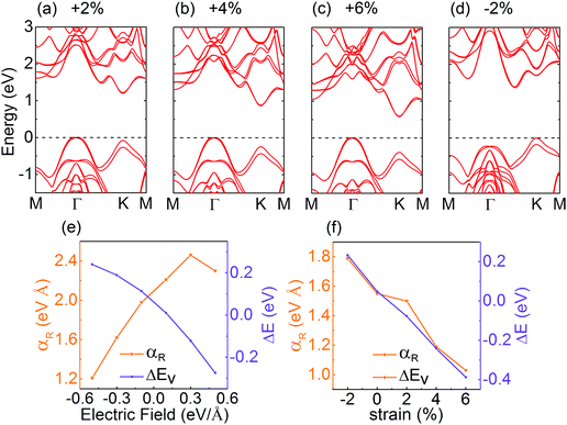
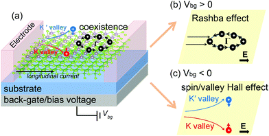
The band structures of the BSe/MoSe2 heterostructure with the external electric field varying from −0.5 V Å−1 to +0.5 V Å−1 are shown in Fig. 6. The external electric field in the out-of-plane direction is applied by inserting a dipole layer in the middle of the vacuum region, and the magnitude of the dipole layer is self-consistently determined by making the electric field in the vacuum region away from the slab be a preset value during the calculations. The external electric field perpendicular to the interface heterostructure can regulate the electronic structure of the system by influencing the interface dipole behavior. In our calculations, the positive (negative) direction of the external electric field is defined as that pointing from BX (MX2) to MX2 (BX). The initial value of the external electric field is set to +0.1 V Å−1 (−0.1 V Å−1) and increases by that unit thereafter. The pristine MoSe2 monolayer has a direct band-gap with the VBM and CBM located at the K point (Fig. S1(b), ESI†). After the formation of heterostructures, due to the presence of electron transfer from BSe to MoSe2, the valence-band edge around the Γ point shifts to higher energy and approaches that at the K point. Obviously, by further applying a positive electric field to promote the charge transfer at the interface, the bands at the Γ point can be further moved to higher energy, and the VBM shifts from the K to the Γ point at a small positive electric field. Meanwhile, the spin characteristics at the VBM of the system are mainly represented by the in-plane direction induced by the Rashba splitting. In contrast, a negative electric field can suppress the charge transfer at the interface, and the valence-band edge gradually recover to the appearance similar to that of the monolayer MoSe2. The electron spin characteristics around the VBM are mainly manifested as the out-of-plane spin induced by valley polarization. The generalized Rashba parameter aR and the relative energy shift ΔE = EKVBM − EΓVBM between the valence-band edges around K and Γ points are shown in Fig. 7(e). It is found that the Rashba parameter aR has almost doubled as the electric field is changed from −0.5 V Å−1 to +0.5 V Å−1. The ΔE shows a monotonous change, that is, the positive electric field promotes the VBM to shift to the Γ point, while the negative electric field consolidates the VBM at the K point. Considering that the lattice strain could change the interatomic bonding and result in the corresponding variation of the electronic properties, we applied a biaxial strain of −2% to +6% to this heterostructure. The calculated band structures of the strained systems are shown in Fig. 7(a)–(d). The tensile strain has a similar regulatory effect to the positive electric field, which makes the valence-band edges at the Γ point shift to higher energy, and then undertakes the main contribution of VBM transport. Correspondingly, the compressive strain causes the VBM of the system to be stable at the K point. Therefore, the variation trend of ΔE under different strains is similar to that in electric field regulation. Instead, the Rashba parameter aR of the system decreases monotonically with the strain change from −2% to +6%. For the BSe/WSe2 heterostructure, the regulation effect of the electric field and strain on the energies of the band edges at the Γ and K points is similar to that of the BSe/MoSe2 heterostructure, as shown in Fig. S8 and S9 (ESI†). Due to the large ΔE in its initial state, the regulation effect is less sensitive. In addition, compared with the strain, the external electric field has more advantages in regulating the electronic structure of the system. Applying a positive electric field not only provides an efficient approach to generate an available energy interval lived by only Rashba-type states, but also increases the Rashba parameter aR. These remarkable features make this system suitable for highly efficient spin FETs, where one can exploit the giant 2D Rashba effect to control the spin state of the 2D electron system. Although the tension strain can also provide energy space for Rashba states, its corresponding Rashba parameter aR gradually decreases. Based on the above analysis, Fig. 8(a) shows the schematic of the spin FET based on the BSe/MoSe2 heterostructure. The system has in-plane spin electrons around the Γ point and different electronic spin states in the K/K′ valleys, following three different transport paths in the presence of an in-plane electric field. However, the valence band-edges related to valley polarization and Rashba spin splitting are not degenerate in energy. With a small hole doping, the spin transport of the carriers in the system can be regulated by the back-gate (out-of-plane) electric field, and the bias voltage can make it inclined to the Rashba-type in-plane spin (Fig. 8(b)) or valley polarization related out-of-plane spin (Fig. 8(c)), making it a promising candidate for applications in 2D spin FET and spin/valley Hall effect devices. When the valence band-edge of both K/K′ valleys and Γ point move above the Fermi level by hole doping, we proposed that if an in-plane longitudinal electric field (E) is applied to the device through the electrode, it will drive the carriers near the K/K′ points to move perpendicular to E due to the large transverse velocities, while carriers around the Γ point transport in the direction of E. As a consequence, carriers at different k points can be well separated, making carriers around the Γ point available to transport.
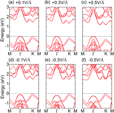 | ||
| Fig. 6 Calculated band structures of the BSe/MoSe2 heterostructure under different electric fields from −0.5 V Å−1 to +0.5 V Å−1. | ||
Conclusions
We perform first-principles calculations to investigate the electronic properties of BX/MX2 (M = Mo or W; X = S, Se and Te) vdW heterostructures, which is a promising platform for studying spin physics with the presence of strong SOC and broken inversion symmetry. The binding energies and phonon dispersion plots are performed to verify the stability of the heterostructures. The calculated band structures reveal that all of them maintain the semiconducting nature, but have different band alignments, which is related to orbital components at the band-edge and influenced by the electron transfer at the interface. By considering the SOC, the Rashba-type spin splitting with in-plane spin and valley polarization with out-of-plane spin can be formed and coexist at the valence-bands of BSe/MoSe2 and BSe/WSe2. Moreover, the location of the VBM can be regulated at the Γ and K points by exerting a biaxial strain and external electrical field. By comparison, the external electric field has more advantages in regulating the electronic structure of the system. Applying a positive electric field not only provides an efficient approach to generate an available energy interval lived by only Rashba-type states, but also increases the Rashba parameter. Consequently, a small hole doping can be used to tune the carrier populations in the different pockets of the Brillouin zone. Since the pockets correspond to different spin directions, this fact gives rise to a new methodology for spin manipulation in spintronics applications.Conflicts of interest
The authors declare no competing financial interest.Acknowledgements
This work was partially supported by the National Natural Science Foundation of China (No. 11704282), the Natural Science Foundation of Tianjin City (No. 18JCQNJC72900), and the Education Commission Research Project of Tianjin City (No. 2017KJ251).References
- H. Fang, S. Chuang, T. C. Chang, K. Takei, T. Takahashi and A. Javey, Nano Lett., 2012, 12, 3788–3792 CrossRef CAS PubMed.
- A. Castellanos-Gomez, M. Poot, G. A. Steele, H. S. van der Zant, N. Agrait and G. Rubio-Bollinger, Adv. Mater., 2012, 24, 772–775 CrossRef CAS PubMed.
- Q. H. Wang, K. Kalantar-Zadeh, A. Kis, J. N. Coleman and M. S. Strano, Nat. Nanotechnol., 2012, 7, 699–712 CrossRef CAS PubMed.
- B. Radisavljevic, A. Radenovic, J. Brivio, V. Giacometti and A. Kis, Nat. Nanotechnol., 2011, 6, 147–150 CrossRef CAS PubMed.
- K. F. Mak, C. Lee, J. Hone, J. Shan and T. F. Heinz, Phys. Rev. Lett., 2010, 105, 136805 CrossRef PubMed.
- A. Splendiani, L. Sun, Y. Zhang, T. Li, J. Kim, C. Y. Chim, G. Galli and F. Wang, Nano Lett., 2010, 10, 1271–1275 CrossRef CAS PubMed.
- D. Xiao, G.-B. Liu, W. Feng, X. Xu and W. Yao, Phys. Rev. Lett., 2012, 108, 196802 CrossRef PubMed.
- Z. Y. Zhu, Y. C. Cheng and U. Schwingenschlögl, Phys. Rev. B: Condens. Matter Mater. Phys., 2011, 84, 153402 CrossRef.
- D. Xiao, W. Yao and Q. Niu, Phys. Rev. Lett., 2007, 99, 236809 CrossRef PubMed.
- A. Rycerz, J. Tworzydło and C. W. J. Beenakker, Nat. Phys., 2007, 3, 172–175 Search PubMed.
- T. Cao, G. Wang, W. Han, H. Ye, C. Zhu, J. Shi, Q. Niu, P. Tan, E. Wang, B. Liu and J. Feng, Nat. Commun., 2012, 3, 887 Search PubMed.
- H. Zeng, J. Dai, W. Yao, D. Xiao and X. Cui, Nat. Nanotechnol., 2012, 7, 490–493 CrossRef CAS PubMed.
- C. K. Safeer, J. Ingla-Aynes, F. Herling, J. H. Garcia, M. Vila, N. Ontoso, M. R. Calvo, S. Roche, L. E. Hueso and F. Casanova, Nano Lett., 2019, 19, 1074–1082 CrossRef CAS PubMed.
- M. K. Mohanta, A. Rawat, N. Jena, Dimple, R. Ahammed and A. De Sarkar, ACS Appl. Mater. Interfaces, 2020, 12, 3114–3126 CrossRef CAS PubMed.
- D. Zhang, Z. Zeng, Q. Tong, Y. Jiang, S. Chen, B. Zheng, J. Qu, F. Li, W. Zheng, F. Jiang, H. Zhao, L. Huang, K. Braun, A. J. Meixner, X. Wang and A. Pan, Adv. Mater., 2020, 32, 1908061 CrossRef CAS PubMed.
- L. Wu, C. Cong, J. Shang, W. Yang, Y. Chen, J. Zhou, W. Ai, Y. Wang, S. Feng, H. Zhang, Z. Liu and T. Yu, Nano Res., 2021, 14, 2215–2223 CrossRef CAS.
- K. Chu, Y. P. Liu, Y. B. Li, Y. L. Guo and Y. Tian, ACS Appl. Mater. Interfaces, 2020, 12, 7081–7090 CrossRef CAS PubMed.
- Y. Dong, Y. Liu, Y. Hu, K. Ma, H. Jiang and C. Li, Sci. Bull., 2020, 65, 1470–1478 CrossRef CAS.
- M. Liao, Z. W. Wu, L. Du, T. Zhang, Z. Wei, J. Zhu, H. Yu, J. Tang, L. Gu, Y. Xing, R. Yang, D. Shi, Y. Yao and G. Zhang, Nat. Commun., 2018, 9, 4068 CrossRef PubMed.
- E. M. Alexeev, D. A. Ruiz-Tijerina, M. Danovich, M. J. Hamer, D. J. Terry, P. K. Nayak, S. Ahn, S. Pak, J. Lee, J. I. Sohn, M. R. Molas, M. Koperski, K. Watanabe, T. Taniguchi, K. S. Novoselov, R. V. Gorbachev, H. S. Shin, V. I. Fal'ko and A. I. Tartakovskii, Nature, 2019, 567, 81–86 CrossRef CAS PubMed.
- B. Li, H. Guo, Y. Wang, W. Zhang, Q. Zhang, L. Chen, X. Fan, W. Zhang, Y. Li and W.-M. Lau, npj Comput. Mater., 2019, 5, 16 CrossRef.
- S. J. Liang, B. Cheng, X. Cui and F. Miao, Adv. Mater., 2019, 32, 1903800 CrossRef PubMed.
- Y. Liu, Y. Huang and X. Duan, Nature, 2019, 567, 323–333 CrossRef CAS PubMed.
- Q. Cui, J. Liang, B. Yang, Z. Wang, P. Li, P. Cui and H. Yang, Phys. Rev. B, 2020, 101, 214439 CrossRef CAS.
- N. Ubrig, E. Ponomarev, J. Zultak, D. Domaretskiy, V. Zolyomi, D. Terry, J. Howarth, I. Gutierrez-Lezama, A. Zhukov, Z. R. Kudrynskyi, Z. D. Kovalyuk, A. Patane, T. Taniguchi, K. Watanabe, R. V. Gorbachev, V. I. Fal'ko and A. F. Morpurgo, Nat. Mater., 2020, 19, 299–304 CrossRef CAS PubMed.
- A. Manchon, H. C. Koo, J. Nitta, S. M. Frolov and R. A. Duine, Nat. Mater., 2015, 14, 871–882 CrossRef CAS PubMed.
- P. Chuang, S. C. Ho, L. W. Smith, F. Sfigakis, M. Pepper, C. H. Chen, J. C. Fan, J. P. Griffiths, I. Farrer, H. E. Beere, G. A. Jones, D. A. Ritchie and T. M. Chen, Nat. Nanotechnol., 2015, 10, 35–39 CrossRef CAS PubMed.
- M. Schultz, F. Heinrichs, U. Merkt, T. Colin, T. Skauli and S. Løvold, Semicond. Sci. Technol., 1996, 11, 1168–1172 CrossRef CAS.
- Y. M. Koroteev, G. Bihlmayer, J. E. Gayone, E. V. Chulkov, S. Blugel, P. M. Echenique and P. Hofmann, Phys. Rev. Lett., 2004, 93, 046403 CrossRef PubMed.
- C. R. Ast, J. Henk, A. Ernst, L. Moreschini, M. C. Falub, D. Pacile, P. Bruno, K. Kern and M. Grioni, Phys. Rev. Lett., 2007, 98, 186807 CrossRef PubMed.
- A. Kimura, E. E. Krasovskii, R. Nishimura, K. Miyamoto, T. Kadono, K. Kanomaru, E. V. Chulkov, G. Bihlmayer, K. Shimada, H. Namatame and M. Taniguchi, Phys. Rev. Lett., 2010, 105, 076804 CrossRef CAS PubMed.
- Z. H. Zhu, G. Levy, B. Ludbrook, C. N. Veenstra, J. A. Rosen, R. Comin, D. Wong, P. Dosanjh, A. Ubaldini, P. Syers, N. P. Butch, J. Paglione, I. S. Elfimov and A. Damascelli, Phys. Rev. Lett., 2011, 107, 186405 CrossRef PubMed.
- P. D. King, R. C. Hatch, M. Bianchi, R. Ovsyannikov, C. Lupulescu, G. Landolt, B. Slomski, J. H. Dil, D. Guan, J. L. Mi, E. D. Rienks, J. Fink, A. Lindblad, S. Svensson, S. Bao, G. Balakrishnan, B. B. Iversen, J. Osterwalder, W. Eberhardt, F. Baumberger and P. Hofmann, Phys. Rev. Lett., 2011, 107, 096802 CrossRef CAS PubMed.
- D. Di Sante, P. Barone, R. Bertacco and S. Picozzi, Adv. Mater., 2013, 25, 509–513 CrossRef CAS PubMed.
- M. Sakano, M. S. Bahramy, A. Katayama, T. Shimojima, H. Murakawa, Y. Kaneko, W. Malaeb, S. Shin, K. Ono, H. Kumigashira, R. Arita, N. Nagaosa, H. Y. Hwang, Y. Tokura and K. Ishizaka, Phys. Rev. Lett., 2013, 110, 107204 CrossRef CAS PubMed.
- T.-H. Wang and H.-T. Jeng, npj Comput. Mater., 2017, 3, 5 CrossRef.
- K. Wu, J. Chen, H. Ma, L. Wan, W. Hu and J. Yang, Nano Lett., 2021, 21, 740–746 CrossRef CAS PubMed.
- J. Sławińska, F. T. Cerasoli, P. Gopal, M. Costa, S. Curtarolo and M. Buongiorno Nardelli, 2D Mater, 2020, 7, 025026 CrossRef.
- S. Singh and A. H. Romero, Phys. Rev. B, 2017, 95, 165444 CrossRef.
- Q. Zhang and U. Schwingenschlögl, Phys. Rev. B, 2018, 97, 155415 CrossRef CAS.
- H. U. Din, M. Idrees, A. Albar, M. Shafiq, I. Ahmad, C. V. Nguyen and B. Amin, Phys. Rev. B, 2019, 100, 165425 CrossRef CAS.
- S. Sattar and J. A. Larsson, ACS Appl. Electron. Mater., 2020, 2, 3585–3592 CrossRef CAS.
- C.-W. Yang, H.-L. Tang, S. Sattar, M.-H. Chiu, Y. Wan, C.-H. Chen, J. Kong, K.-W. Huang, L.-J. Li and V. Tung, ACS Mater. Lett., 2020, 2, 1351–1359 CrossRef CAS.
- D. Khokhriakov, A. M. Hoque, B. Karpiak and S. P. Dash, Nat. Commun., 2020, 11, 3657 CrossRef CAS PubMed.
- J. F. Sierra, J. Fabian, R. K. Kawakami, S. Roche and S. O. Valenzuela, Nat. Nanotechnol., 2021, 16, 856–868 CrossRef CAS PubMed.
- Q.-F. Yao, J. Cai, W.-Y. Tong, S.-J. Gong, J.-Q. Wang, X. Wan, C.-G. Duan and J. H. Chu, Phys. Rev. B, 2017, 95, 165401 CrossRef.
- R. Li, Y. Cheng and W. Huang, Small, 2018, 14, 1802091 CrossRef PubMed.
- W. Zhou, J. Chen, Z. Yang, J. Liu and F. Ouyang, Phys. Rev. B, 2019, 99, 075160 CrossRef.
- L. Zhu, Y. Zhang, P. Lin, Y. Wang, L. Yang, L. Chen, L. Wang, B. Chen and Z. L. Wang, ACS Nano, 2018, 12, 1811–1820 CrossRef CAS PubMed.
- C. S. Ho, W. Kong, M. Yang, A. Rusydi and M. B. A. Jalil, New J. Phys., 2019, 21, 103016 CrossRef CAS.
- H.-F. Huang, Y.-J. Dong, Y. Yao, J.-Y. Zhang, X. Hao, H. Gu and Y.-Z. Wu, J. Appl. Phys., 2020, 128, 224105 CrossRef CAS.
- S. Demirci, N. Avazlı, E. Durgun and S. Cahangirov, Phys. Rev. B, 2017, 95, 115409 CrossRef.
- G. Kresse and D. Joubert, Phys. Rev. B: Condens. Matter Mater. Phys., 1999, 59, 1758–1775 CrossRef CAS.
- J. P. Perdew, K. Burke and M. Ernzerhof, Phys. Rev. Lett., 1996, 77, 3865–3868 CrossRef CAS PubMed.
- G. Kresse and J. Furthmüller, Phys. Rev. B: Condens. Matter Mater. Phys., 1996, 54, 11169–11186 CrossRef CAS PubMed.
- P. E. Blochl, Phys. Rev. B: Condens. Matter Mater. Phys., 1994, 50, 17953–17979 CrossRef PubMed.
- J. Heyd, G. E. Scuseria and M. Ernzerhof, J. Chem. Phys., 2003, 118, 8207–8215 CrossRef CAS.
- J. Heyd and G. E. Scuseria, J. Chem. Phys., 2004, 121, 1187–1192 CrossRef CAS PubMed.
- S. Grimme, J. Comput. Chem., 2004, 25, 1463–1473 CrossRef CAS PubMed.
- A. Togo and I. Tanaka, Script. Mater., 2015, 108, 1–5 CrossRef CAS.
- U. Herath, P. Tavadze, X. He, E. Bousquet, S. Singh, F. Muñoz and A. H. Romero, Comput. Phys. Commun., 2020, 251, 107080 CrossRef CAS.
- Z. Y. Zhu, Y. C. Cheng and U. Schwingenschlögl, Phys. Rev. B: Condens. Matter Mater. Phys., 2011, 84, 153402 CrossRef.
- G. Graziano, J. Klimes, F. Fernandez-Alonso and A. Michaelides, J. Phys.: Condens. Matter, 2012, 24, 424216 CrossRef PubMed.
- P. Lou and J. Y. Lee, ACS Appl. Mater. Interfaces, 2020, 12, 14289–14297 CrossRef CAS PubMed.
- K. Ren, W. Tang, M. Sun, Y. Cai, Y. Cheng and G. Zhang, Nanoscale, 2020, 12, 17281–17289 RSC.
- J. Song, H. Zheng, M. Liu, G. Zhang, D. Ling and D. Wei, Phys. Chem. Chem. Phys., 2021, 23, 3963–3973 RSC.
- K. Kośmider and J. Fernández-Rossier, Phys. Rev. B: Condens. Matter Mater. Phys., 2013, 87, 075451 CrossRef.
- L. Huang, N. Huo, Y. Li, H. Chen, J. Yang, Z. Wei, J. Li and S. S. Li, J. Phys. Chem. Lett., 2015, 6, 2483–2488 CrossRef CAS PubMed.
- Z. Huang, C. He, X. Qi, H. Yang, W. Liu, X. Wei, X. Peng and J. Zhong, J. Phys. D: Appl. Phys., 2014, 47, 075301 CrossRef CAS.
- Y. C. Cheng, Z. Y. Zhu, M. Tahir and U. Schwingenschlögl, Europhys. Lett., 2013, 102, 57001 CrossRef.
- T. Hu, F. Jia, G. Zhao, J. Wu, A. Stroppa and W. Ren, Phys. Rev. B, 2018, 97, 235404 CrossRef CAS.
- J. Chen, K. Wu, H. Ma, W. Hu and J. Yang, RSC Adv., 2020, 10, 6388–6394 RSC.
- Y. Wang, W. Wei, H. Wang, N. Mao, F. Li, B. Huang and Y. Dai, J. Phys. Chem. Lett., 2019, 10, 7426–7432 CrossRef CAS PubMed.
- Y. A. Bychkov and E. I. Rashba, JETP Lett., 1984, 39, 78–81 Search PubMed.
- L. Xiang, Y. Ke and Q. Zhang, Appl. Phys. Lett., 2019, 115, 203501 CrossRef.
- D. Xiao, G. B. Liu, W. Feng, X. Xu and W. Yao, Phys. Rev. Lett., 2012, 108, 196802 CrossRef PubMed.
- E. A. de Andrada e Silva, G. C. La Rocca and F. Bassani, Phys. Rev. B: Condens. Matter Mater. Phys., 1994, 50, 8523–8533 CrossRef CAS PubMed.
- J. D. Sau, R. M. Lutchyn, S. Tewari and S. Das Sarma, Phys. Rev. Lett., 2010, 104, 040502 CrossRef PubMed.
- S. Gupta, S. N. Shirodkar, A. Kutana and B. I. Yakobson, ACS Nano, 2018, 12, 10880–10889 CrossRef CAS PubMed.
Footnote |
| † Electronic supplementary information (ESI) available. See DOI: 10.1039/d1tc03662a |
| This journal is © The Royal Society of Chemistry 2022 |

