
Facile template-free preparation of silver-coated Cu3SbS4 hollow spheres with enhanced photoelectric properties†
Xiang
Meng
 a,
Xihao
Chen
ab,
Jiang
Cheng
a,
Fuqiang
Zhai
a,
Wen
Li
c,
Rui
Hu
d and
Lu
Li
*a
a,
Xihao
Chen
ab,
Jiang
Cheng
a,
Fuqiang
Zhai
a,
Wen
Li
c,
Rui
Hu
d and
Lu
Li
*a
aSchool of Material Science and Engineering, Chongqing University of Arts and Sciences, Chongqing 402160, China. E-mail: lli@cqwu.edu.cn
bDepartment of Physics, Chongqing University, Chongqing, 400044, China
cInterdisciplinary Materials Research Center, School of Materials Science and Engineering, Tongji Univ., 4800 Caoan Rd., Shanghai 201804, China
dKey Laboratory of Photovoltaic and Energy Conservation Materials, Institute of Solid State Physics, Hefei Institutes of Physical Science, Chinese Academy of Sciences, Hefei 230031, China
First published on 23rd November 2021
Abstract
Hollow polycrystalline structures and noble-metal-coating endow ternary sulfides with promising light absorption and electrical properties for solar energy conversion applications. We developed a facile one-pot solvothermal chemical route to synthesize hollow Cu3SbS4 microspheres with an opening. Additionally, four phase-pure Cu–Sb–S high-quality nanocrystals can be produced in a selectable way by the same route. The detailed evolution process and self-driven breakage mechanism have been proposed in detail. Subsequently, in situ reduction of the Ag-ion precursor was conducted and Ag clusters were uniformly deposited in the hollow spherical architecture with a nanoparticle-textured surface and interior to mitigate the oxidization of Cu3SbS4 nanoparticles. The created hollow metal-semiconductor nanocomposite opens up a favorable new situation. The nanocomposites exhibited a remarkably enhanced absorption of over 2 × 105 cm−1, covering the UV and visible regions of the electromagnetic spectrum. The electrical resistivity decreased drastically by 90% after the coating of noble metals. A reduction in the bandgap energy after the addition of Ag to Cu3SbS4 was confirmed from extrapolated optical results and theoretical calculation validation. The synthetic effect of hollow structures and nanocomposites results in the superior performance of Cu–Sb–S compounds, thus highlighting their potential applications in light absorbers and energy conversion technologies.
1. Introduction
Solar energy conversion devices have been enhanced incessantly to solve the urgent problems of non-renewable resource shortage and environmental pollution. Among these devices, thin-film solar cells are a constant pursuit because of their inherent low cost, effectiveness, lightweight, feasible flexibility and ongoing rising conversion efficiency.1,2 Considerable effort has been devoted to discovering nontoxic and more earth-abundant alternative materials with a higher light absorption than that of commercially available CuInGaSe2 (CIGS) and CdTe.3,4 Many chalcogenides with a high absorption coefficient of over 104 cm−1 and an optimum bandgap range of 0.9–1.5 eV meet the prerequisite above, such as Cu–Zn–Sn–S–Se (CZTS or CZTSSe),5,6 SnS,7 Ba–Cu–S8 and Cu–Sb–S,2,9–14 and have been proposed as absorber materials for photovoltaic thin-film technologies. The record power conversion efficiency of CZTSSe has reached 12.6%,15 followed by numerous studies on other promising polynary copper-based sulfides.Cu3SbS4, Cu12Sb4S13, CuSbS2 and Cu3SbS3, four phases of the ternary Cu–Sb–S (CAS) system, contain inexpensive and abundant elements and are expected to be of interest for a broad range of applications. The chalcostibite CuSbS2 with a favorable bandgap of 1.55 eV has attracted much attention for research and utilization in thin-film solar cells.9,14 In our previous work2, we synthesized Ag-substituted CuSbS2 films as the light-absorption layer material, and the efficiency of the device was significantly promoted by 2.48%. The tetrahedrite Cu12Sb4S13 is being regarded as a competitive p-type thermoelectric material due to its ultralow lattice thermal conductivity of under 0.6 W mK−1 originating from its complex structure with rattler atoms.16,17 The famatinite Cu3SbS4 with a tetragonal structure has a bandgap of around 1.0 eV, deep valence band positions, a high hole carrier mobility (1.7 cm2 V−1 s−1) and high absorption coefficient (105 cm−1).18–20 The electron and hole relaxation dynamics of CAS compounds have been measured, and the carriers in Cu3SbS4 possessed a suitable lifetime of ∼5 picoseconds before trapping.21 Although these properties and the first-principles calculations22 have made Cu3SbS4 an outstanding material for potential thin-film solar cell applications, Cu3SbS4-involved devices have only received low efficiencies to date. Several strategies have been proposed to improve the optical absorption and transport of carriers as well as the solar energy conversion performance of devices related to CAS.
There are no materials like nanomaterials, let alone gather into specific structures. Nanocrystals composing hollow structures with interior cavities have been intentionally developed for solar cell, photocatalysis and photo-relevant applications23–29 due to their high-surface-area, low-weight and distinct hollow features, which greatly enhances light absorption efficiency by multiple light diffraction and reflection effect within the interior cavities.25 Furthermore, the shortened path of electronic or mass transport by hollow structures also leads to rapid separation of electron and hole and effectively decreases their recombination rate.24,26,28,30 Various types of hollow metal-sulfides structures, such as spheres,27,31,32 cubes33,34 and tubes,30,35 have been synthesized and obtained showing consequential enhanced photoelectric performance. Normally, binary compounds (Sb2S3,36,37 NiS,38 CoS2,27,39 CdS,25 CuS40), but not complex ternary compounds with a hollow sphere structure (such as CAS compounds), have been synthesized by tedious processes for photovoltaic applications. The detailed evolution processes and reasons for self-driven breakage are still vague, which led us to explore the formation of hollow ternary CAS structures. Meanwhile, Albuquerque has demonstrated that the preferential thin oxidized Cu2+ layer on the surface of the Cu3SbS4 nanocrystal film significantly limited the photoelectric performance of solar cells.11 The surface treatment or compositing with noble metals, such as silver (Ag), may tackle this problem. The light absorption would be enhanced due to the surface plasmon resonance absorption of Ag and tunable electronic band structure of the host material.41 Meanwhile, the introduction of noble metals not only brings a high light sensitizing ability and reliable conductivity42,43 but also the synergistic effect from different energy levels with sulfides.44,45 The as-synthesized composites have been designed for various applications of optics,46 solar cells,47 photocatalysis.30,31 Accordingly, the large surface area with a rough surface of the hollow sphere nanostructure provides ideal adsorption sites for metal–ion source nanoparticles. Can a superior all-around performance for solar energy conversion applications be obtained from the synergistic effect of hollow structures and nanocomposites?
The solvothermal method has been widely adopted to synthesize sulfide nanomaterials.12,24 It is a simple method and can be used to efficiently produce nanomaterials at a large scale. However, a mix-phase powder was always obtained because of the narrow thermodynamic stability window of CAS in conventional processes. It remains a great challenge to synthesize phase-controlled phase-pure CAS nanocrystals and understand the formation mechanism. In this study, a facile one-pot solvothermal chemical route has been developed to synthesize monodisperse phase-pure CAS nanocrystals (Cu3SbS4, Cu12Sb4S13, CuSbS2 and Cu3SbS3) in a selectable way. The Cu3SbS4 nanocrystals were assembled to construct the distinctively special hollow microspheres with an opening. Afterward, in situ reduction of Ag+ was conducted and Ag clusters were introduced into the hollow structure to construct a metal-semiconductor nanocomposite. The hybrid exhibited a remarkably enhanced absorption of over 2 × 105 cm−1 covering UV and visible regions of the electromagnetic spectrum, but not a nominal composite. The band structure was systematically investigated by extrapolated optical gaps and theoretical calculations. A reduction in the bandgap energy by the addition of Ag to Cu3SbS4 was confirmed. The electrical resistivity decreases drastically from 0.88 Ω cm to 0.08 Ω cm by the coating of Ag. Meanwhile, the inside-outside diffusion solvothermal mechanism was proposed to elucidate the formation of the hollow microspheres with an opening in the solution. This work demonstrated that the famatinite hollow nanospheres with a noble metal coating could potentially solve problems like low efficiency, low open-circuit voltage and low fill factor values of thin-film solar panels.
2. Experimental
2.1 Synthesis of Cu–Sb–S nanocrystals
Copper(II) acetate monohydrate (99%), antimony acetate (99.99%), thiourea (99%), anhydrous acetic acid (99.8%), 2-methoxyethanol (CH3OCH2CH2OH, 2-ME, 99%), diethanolamine (HO(CH2)2NH(CH2)2OH, DEA, 99%), oleylamine (OLA, 90%), silver nitrate (99%), sodium borohydride (98%) were all ordered from Aladdin Chemicals (Shanghai, China) and used without further purification.CAS nanocrystals were synthesized by a practical one-pot solvothermal method. In a typical synthesis of Cu3SbS4, 9 mmol Cu(CH3COO)2·H2O was loaded into 250 mL of 2-ME solution and completely dissolved with stirring. After that, 0.5 mL DEA, 72 mmol thiourea, and 3 mmol of antimony precursor were dissolved successively. The antimony precursor was prepared by dissolving antimony acetate powder in glacial acetic acid under N2 gas protection in a glove box. The color of the solution changed from turquoise to bluish violet, then to transparent pale yellow, and finally to transparent white. Then, the prepared solution without precipitation was transferred in a Teflon-lined autoclave with a stainless steel shell. The autoclave was heated and maintained at 240 °C for 12 h before being cooled to room temperature. The solution was centrifuged at 10![[thin space (1/6-em)]](https://www.rsc.org/images/entities/char_2009.gif) 000 rpm for 10 min several times by using ethanol and acetone as the dispersing solution, respectively. The upper clear solution was decanted continually, and the isolated particles were finally dried in a vacuum oven at 60 °C for 6 h. For the synthesis of the other three Cu–Sb–S phases, the preparation procedure was the same, but the ratios of elements, temperature and duration time were varied severally.
000 rpm for 10 min several times by using ethanol and acetone as the dispersing solution, respectively. The upper clear solution was decanted continually, and the isolated particles were finally dried in a vacuum oven at 60 °C for 6 h. For the synthesis of the other three Cu–Sb–S phases, the preparation procedure was the same, but the ratios of elements, temperature and duration time were varied severally.
2.2 Coating of Ag on hollow spheres
The as-synthesized Cu3SbS4 hollow spheres were used as hosts for the incorporation of Ag nanoparticles. Firstly, Ag+ ions were adsorbed on the surface and interspaces by soaking spheres in the silver nitrate (0.1 mmol L−1) solution for 2 h. Then, sodium borohydride was added to the solution to coat Ag onto the surface. The reduction of Ag produced a vivid yellow solution. The metal-semiconductor composite precipitates were obtained by the above-mentioned precipitation/dispersion cycles at room temperature.2.3 Measurements and characterization
CAS nanocrystals and composites were analyzed using X-ray diffraction (XRD, D8 Advance, Bruker) with graphite monochromatic Cu Kα radiation (λ = 0.154 nm). The size of particles was calculated roughly according to the Scherrer equation,50D = Kλ/βcosθ, where K is a dimensionless constant, λ is the XRD wavelength, β is the line-broadening at half of the maximum peak intensity and θ is the Bragg angle. The microstructural properties were studied using the Carl Zeiss GeminiSEM 300 field emission scanning electron microscope (SEM) with an energy dispersive spectrometer (EDS). Transmission electron microscopy (TEM) and high-resolution transmission electron microscopy (HRTEM) images were obtained on a JEM 2100F field-emission transmission electron microscope. The chemical composition and distribution were analyzed by X-ray photoelectron spectroscopy (XPS, Escalab 250xi, Thermo Scientific) operating at constant analyzer energy mode. The binding energies were calibrated by referencing C 1s. The intensity ratios of different binding energy peaks for several elements were set as reported.51 The optical properties of products were characterized using a UV–VIS–NIR spectrophotometer (Cary 5000, Agilent) equipped with an integrating sphere attachment using the as-prepared dry powers of nanocrystals. The optical bandgaps were estimated from (αhν)1/2vs. hν plots by extrapolating the linear part of the function.52 Layer thicknesses were measured using a Veeco Dektak surface profiler. Electric properties were measured with a Hall measurement system (H5000, MMR technology) with a temperature-control system (K2000). Samples for Hall measurements were fabricated by a hot-pressing procedure under a pressure of 80 MPa at 673 K for 20 minutes.
2.4 Density functional theory calculation
Density functional theory (DFT) calculations were performed using the Vienna Ab-initio Simulation Package (VASP) code.53 The generalized gradient approximation (GGA)54 and the projector augmented wave (PAW) approach55 were applied to obtain the optimized structures. The kinetic cut-off energy was set as 390 eV. The criterion of energy convergence for atomic positions and lattice parameters was 1 × e−5 eV. The Hellmann–Feynman forces on each atom were converged within −0.01 eV Å. The output structures and density of states (DOS) were relaxed by the hybrid functional method (HSE06). To avoid the coupling effects triggered by periodic structures, the periodic images of the slab were separated by a vacuum region of 20 Å. Brillouin zones with Γ-centered k grids of 6 × 6 × 3 and 5 × 4 × 1 were used for Cu3SbS4 and the one with addition of Ag clusters, respectively.3. Results and discussions
Copper antimony sulfide nanocrystals were synthesized through a facile solvothermal route. The XRD pattern of as-synthesized powder is shown in Fig. 1(a). The diffraction peaks with high intensity corresponding only to famatinite Cu3SbS4 can be clearly observed (JCPDS card No. 35-0581). The sharp diffraction peaks indicate that high purity and crystallinity of the products were obtained, compared to other CAS results by solvothermal,12 hot-injection,11,19,56–58 and hydrothermal methods.59 As shown in Fig. 1(b and c), polyhedral Cu3SbS4 nanoparticles were generated. The inset in Fig. 1(b) exhibits the curve of the size distribution of the as-synthesized nanocrystals. Interestingly, there are obviously two peaks with high distribution at about 53 nm and 105 nm. However, the estimated calculation diameter from the full-width half maximum of the characteristic peak is about 60 nm. Why were there two sizes of nanocrystals? The HRTEM image and converted FFT image (Fig. 1(d)) of the selected region of nanocrystals in Fig. 1(c) show the perfect single-crystal structure of Cu3SbS4 and no amorphous edges were observed. Spacings of 0.31 nm and 0.47 nm with angles of 39.4° and 78.8° corresponding to (1![[1 with combining macron]](https://www.rsc.org/images/entities/char_0031_0304.gif)
![[2 with combining macron]](https://www.rsc.org/images/entities/char_0032_0304.gif) ) and (10) planes, respectively, which is consistent with the XRD result were observed. It is worth noting that all four pure CAS phases were fabricated selectively and successfully through the same solvothermal route; XRD patterns and microstructures of other phases are shown in Fig. S1 (ESI†). The nanocrystals presented different outline features, such as irregular, trigonal-pyramidal and two-dimensional sheets morphology for Cu3SbS4, Cu12Sb4S13 and CuSbS2, respectively.
) and (10) planes, respectively, which is consistent with the XRD result were observed. It is worth noting that all four pure CAS phases were fabricated selectively and successfully through the same solvothermal route; XRD patterns and microstructures of other phases are shown in Fig. S1 (ESI†). The nanocrystals presented different outline features, such as irregular, trigonal-pyramidal and two-dimensional sheets morphology for Cu3SbS4, Cu12Sb4S13 and CuSbS2, respectively.
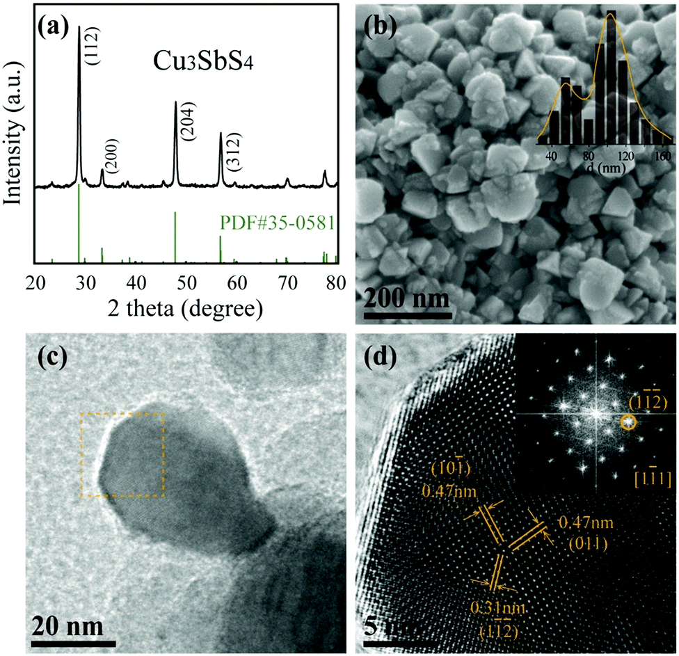 | ||
| Fig. 1 (a) XRD patterns of the as-synthesized Cu3SbS4 sample along with the standard reference pattern. (b) SEM image of Cu3SbS4 nanocrystals along with the inset of the size distribution histogram of the sample. (c) TEM image of Cu3SbS4 monocrystals. (d) HRTEM image as well as FFT image as the inset. | ||
XPS measurements were conducted to confirm the surface bonding state of CAS nanocrystals prepared using the solvothermal method. As shown in Fig. 2, elements Cu, Sb, S, except C, N and O could be observed on survey scans of all CAS samples. In a high-resolution spectrum, the chemical state of Cu 2p distinctly occupied two peaks located at 952.2 and 932.3 eV, which can be attributed to Cu (2p1/2) and Cu (2p3/2) binding states, respectively.10,60,61 The peak splitting with 19.9 eV indicated Cu in Cu3SbS4 is in the form of Cu+ and no oxidation happened on the surface. As shown in Fig. S2 (ESI†), there are Cu(2P3/2) satellite peaks located at about 962.0 and 942.0 eV as marked by arrows for the contribution from Cu2+ in Cu12Sb4S13, besides the two peaks for the Cu+ oxidation state.19 The core-level spectrum of Sb 3d shows the line fit excellently to a 3d spin–orbit split doublet at 528.9 (3d5/2) and 538.3 eV (3d3/2) with a split orbit of 9.4 eV, which is consistent with that of Sb5+ in a thiourea-rich environment for Cu3SbS4.13 However, element Sb in Cu12Sb4S13 possessed two chemical valence states of Sb5+ and Sb3+ according to two broad peaks.62 The splitting two peaks position, separations and relative intensities of S 2p are consistent with S2− in all CAS compounds.11
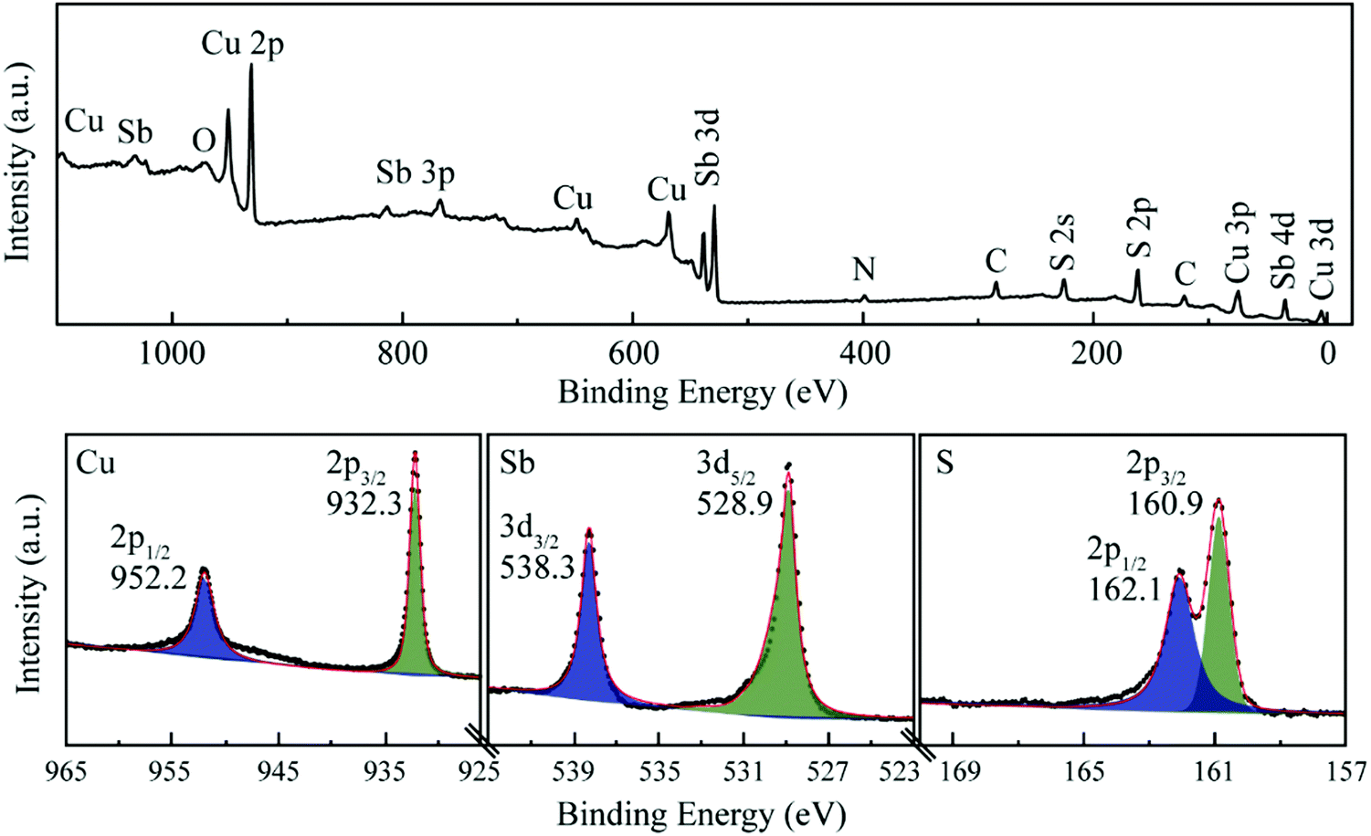 | ||
| Fig. 2 XPS spectra of the as-synthesized Cu3SbS4 nanocrystals, including the survey spectrum along with the corresponding high-resolution XPS spectra for the Cu 2p, Sb 3d, and S 2p core levels. | ||
A series of low magnification SEM images of the as-synthesized Cu3SbS4 nanocrystals are shown in Fig. 3. It can be observed that the nanocrystals are not monodispersed, but closely combined to form the nanoparticles-textured microsphere structure. The microspheres with a diameter of 0.9–1.1 μm were dispersed homogeneously. The higher magnification images in (b) and (c) show that the microspheres are particularly hollow and broken with an opening. Although the proportion of the microspheres with an opening appeared to be only about 10% from the SEM observation, the actual proportion is expected to be larger due to the limited vision. The hollow spherical structure and unique nanoparticles-textured surface would be beneficial for enhancing the light absorption, efficient transport pathways and separation of electrons and holes.23–26 Meanwhile, the large superficial area with a rough surface provides ideal adsorption sites for metal–ion sources nanoparticles, which would introduce better optical and electric properties.
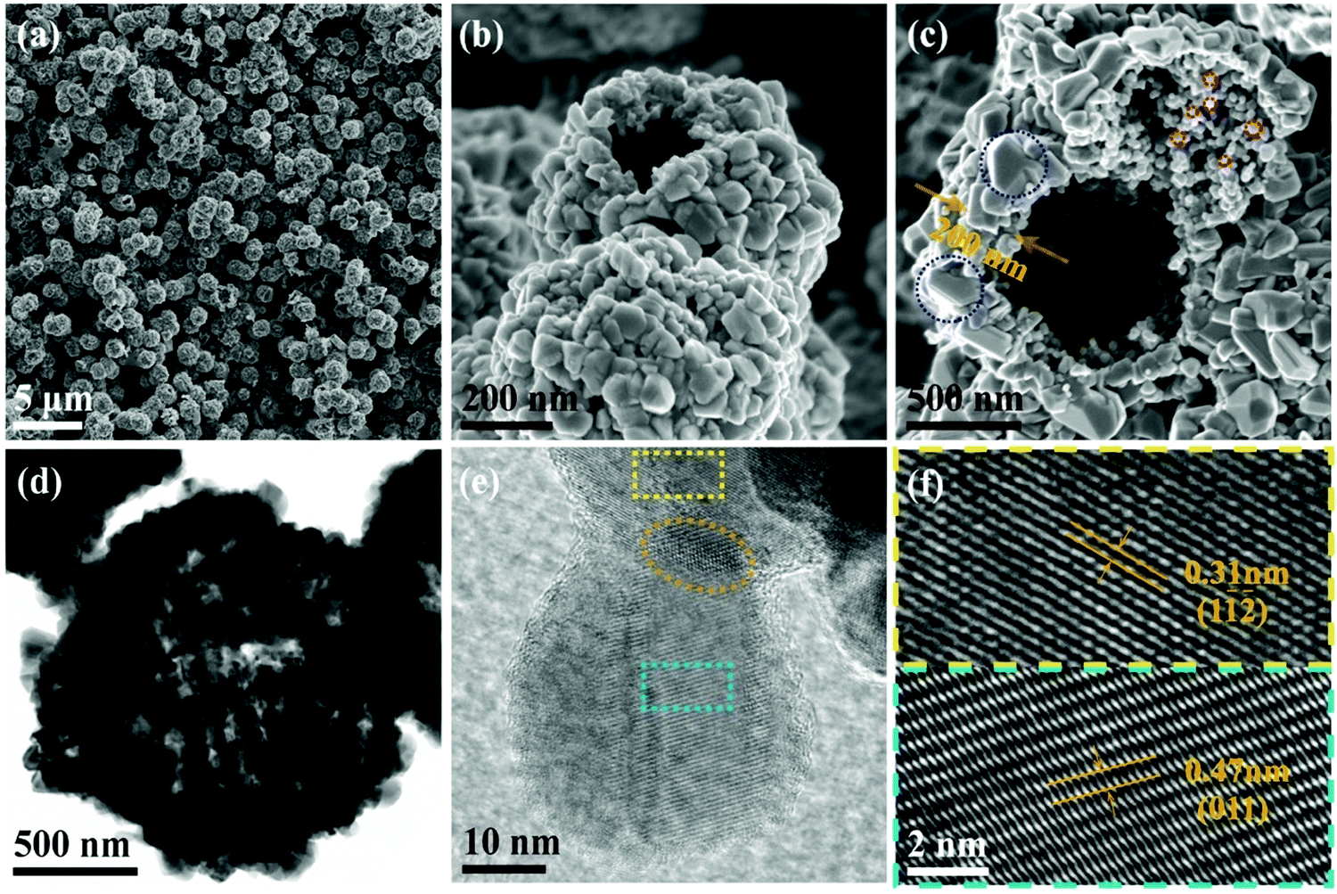 | ||
| Fig. 3 (a) Low-magnification SEM image; (b) and (c) high-magnification SEM images of the as-synthesized hollow Cu3SbS4 spheres consisting of nanocrystals, especially the ones with an opening. (d) TEM image of the hollow sphere. (e) and (f) HRTEM images of Cu3SbS4 nanocrystals and their connection. | ||
The shell of hollow microspheres with a thickness of about 200 nm at a certain stage of growth consists of big particles outside (marked in blue circle) and small nanoparticles inside (marked in red circle), as shown in Fig. 3(c). The two distinctly different sizes of crystals are close to the statistical data in Fig. 1(b). The unique morphology may give some hint on the formation of Cu3SbS4 hollow microspheres. TEM and HRTEM results on Cu3SbS4 samples are also shown in Fig. 3. The hollow microsphere can be identified by the high contrast in the middle of the volleyball-like structure. The electron penetration could be observed in the microsphere, which suggests the existence of voids or openings. To test the mechanical property and stability of the microsphere, the ultrasonic treatment for a long time was conducted before the centrifugal treatment, but the spheres were not broken in the solution, indicating that the nanocrystals were attached with each other through some connection. The HRTEM image of Fig. 3(e) shows a Cu3SbS4 nanoparticle connecting the other one. The lattice fringes of the two domains belong to the Cu3SbS4 phase. The zone axis of two planes (marked in a yellow and cyan rectangle) could be all in the [11] direction, as shown in Fig. 3(f). There may be a junction or overlap (marked in ginger ellipse) between the single crystals.
As stated previously, there is no doubt that polycrystalline Cu3SbS4 hollow microspheres would be superior to regular particle structures as supports for noble-metal nanoparticles and thus are endowed with the improved optical and electric properties for the following reasons: (i) the distinct hollow structure for light trapping and depressed carriers recombination; (ii) the large rough surface and open interior for loading nanoparticles; (iii) surface plasmon resonance absorption and high electric conductivity of noble-metal; (iv) mitigation of oxidation of the Cu3SbS4 surface and guaranteed stability as absorber layers for thin-film solar cells. Fig. 4 shows the results of hollow Cu3SbS4 microspheres after incorporation of Ag. Element mapping analysis shows that elements Cu, Sb, S and Ag are uniformly distributed over the whole structure. We can see that the element Ag occupied more interior space with a brighter yellow. The average atomic ratio of the Ag element was about 1.98% for 1 vol% Ag within the Cu3SbS4-Ag heterostructure, as shown in Fig. S3 (ESI†). From XRD patterns in Fig. 4(b), the crystalline Ag phase has been synthesized and no other phases could be matched in the composite, but Cu3SbS4 phases. The grain size of Ag could be roughly estimated as 5 nm from XRD results (Cu3SbS4-Ag). There was no obvious change in the bonding state in Cu3SbS4 crystals, as shown in Fig. S4 (ESI†). In the high-resolution XPS spectrum of Ag 3d shown in Fig. 4(c), the two peaks located at about 367.4 and 373.4 eV can be indexed to metallic Ag 3d5/2 and 3d3/2, respectively. The splitting of the doublet was 6.0 eV, which also verified the synthesis of metallic silver.29,42 There was no shift, splitting or satellite peak, and thus no presence of oxidized states.48,63 We demonstrated that the Ag crystal was successfully decorated on the surface and interior of Cu3SbS4 microspheres, and the chemical transformation did not destroy the spherical morphology and composition of Cu3SbS4.
 | ||
| Fig. 4 (a) SEM image and EDS elemental mapping images of the Ag-coated hollow Cu3SbS4 spheres along with the relative chemical composition. (b) XRD patterns of Ag-coated Cu3SbS4 and the as-synthesized Ag nanoparticles along with the standard reference pattern of Ag. (c) High-resolution XPS spectrum for the Ag 2d core level. | ||
After coating Ag, the optical absorption and electric properties for the hollow Cu3SbS4 microspheres were surveyed by UV–Vis absorption and Hall measurements. The absorption coefficient α is shown in Fig. 5. The estimation of α could be obtained using the following formula by minimizing the interference effects:64

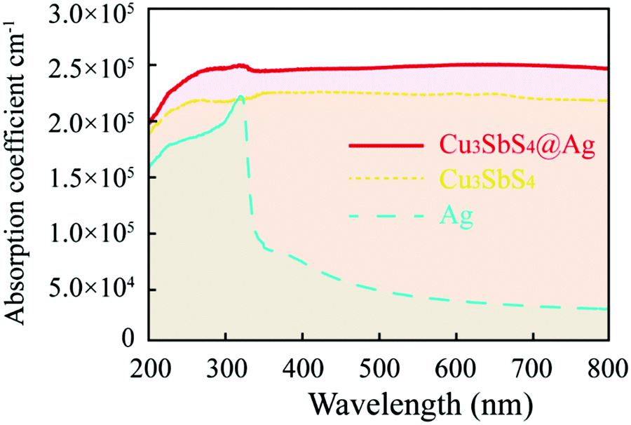 | ||
| Fig. 5 UV–Vis spectra of Ag, hollow Cu3SbS4 spheres and Cu3SbS4@Ag. | ||
| Sample | Electrical resistivity (Ω cm) | Carrier concentration (cm−3) | Carrier mobility (cm2 V−1 s−1) |
|---|---|---|---|
| Cu3SbS4 | 8.83 × 10⁻¹ | 3.1 × 10¹⁹ | 2.34 |
| Cu3SbS4 + 0.5 vol% Ag | 5.14 × 10⁻¹ | 3.35 × 10¹⁹ | 1.61 |
| Cu3SbS4 + 1 vol% Ag | 8.1 × 10⁻² | 8.24 × 10¹⁹ | 0.92 |
4. Discussion
All four stable CAS phases have been synthesized selectively by the solvothermal process. Even though there was very narrow thermodynamic stability window for CAS phases, several methods have been adopted to fabricate successfully the selective single-phase, mostly by the hot-injection method. As shown in Table S1 (ESI†), Cu3SbS4 nanocrystals or films with various structures and sizes were synthesized for diverse applications. Many variables were also investigated in detail to manipulate phase purity and structure of CAS in those reports and this study, and are the decisive factors in various aspects of nucleation, growth, aggregation and recrystallization, such as precursors, ratio, solvent, ligands, temperature, duration time, degree of filling, and pH as reported sporadically elsewhere.12,56,58,59,71,72 The systematic synthesis mechanism and analysis will be announced to elucidate the synthesis of CAS phases in other places.In short for the Cu3SbS4 phase, the 2-methoxyethanol with a low polarity was used as a solvent in the solvothermal method.2 Small doses of diethanolamine acted both as a surfactant and as the chemical stabilizer of precursors, especially thiourea.73 When the solvothermal equipment provided temperature and pressure at a certain level, the emergence of the supersaturation of monomers would force the quick nucleation. The convection of solution and more effectively solute transport led to the growth of crystal nuclei (mostly binary Cu-S phases at the early stage, then ternary phases), which would end in the small nanocrystals and uniform in all faces, due to the insufficient source of precursors in the solvent and the low polarity of the solvent.61 In other words, solution-processed methods prefer producing nanosized nearly spherical uniform crystals, as shown mostly in Table S1 (ESI†). Actually, the high purity of Cu3SbS4 nanocrystals is not readily available just by selecting the element-source ratio. Based on the formation energy theory and experimental practice, the Cu3SbS4 phase is normally more difficult to be synthesized than Cu12Sb4S13 and CuSbS2.58,71 It is occasionally a subproduct of the Cu12Sb4S13 syntheses. The requisite for the synthesis of single-phase Cu3SbS4 and high purity is a higher content of the sulfide precursor than the elemental ratio in the formula.19,56,71,74 Most of the new reports in Table S1 (ESI†) concur that element Sb would be oxidized to be Sb5+ by the created excessive sulfur source environment. Therefore, element Sb presents the V valence state in Cu3SbS4, also verified from the XPS measurement in this study. Interestingly, element Cu presents a reduced I valence state. A possible reaction process is proposed here. Copper(II) acetate monohydrate and antimony(III) acetate were used as Cu and Sb precursors, respectively. Thiourea is somewhat reductive, and thus Cu2+ would be reduced to Cu+ in an excessive thiourea environment, which could be confirmed by the color change of the solution during the experimental part.75 With the rise in temperature, thiourea will decompose rapidly, with the sulfur source and generation of gases according to the following chemical reactions. Thus, excessive sulfur would oxidize Sb3+ to Sb5+ by a combination of a sulfidic and basic environment.35,71,76,77
| SC(NH2)2 + 3H2O → (NH4)2CO3 + 2H+ + S2− | (1) |
| SC(NH2)2 + 2H2O → 2NH3 + H2S + CO2 | (2) |
| Sb3+ + 4S2− → SbS43− | (3) |
Nanocrystals with different sizes and geometries of the Cu3SbS4 phase have been prepared by solvothermal, hot-injection and solution-based methods, as summarized in Table S1 (ESI†), but not framing specific structures to enhance optical and electric performances so far. The hollow Cu3SbS4 microspheres with enhanced light absorption efficiency and improved electric properties were evolved from ions in the solvent. The evolution process is proposed in Scheme 1 based on the results from multivariate experiments. As many crystal nuclei were growing, they tended to gather into intact, nearly-spherical aggregates with an uneven surface and bonded together, as shown in Fig. S7 (ESI†). The tendency toward spherical morphology can be attributed to lowering the surface free energy of nuclei under high pressure and temperature conditions in the low polar solvent.78 The epitaxial crystal growth would be afterward oriented on the specific crystal faces by the continuous growth model due to the rough solid–liquid interface, so the surface of microspheres became rougher.79 Chen has synthesized the cauliflower-like spherical Cu3SbS4 particles with intersectional nanoflakes using the microwave irradiation method, and it could come down to a similar evolution process, yet with a two-dimensional layer growth model due to the more formative energy.13 Given the formation of a hollow structure, it can be deduced that there existed the Ostwald-ripening process and material transport.23,80 Indeed, this postulation is confirmed surprisingly and directly with our results in Fig. 1 and 3. The inner crystallites (as marked in red in Fig. 3) with a small diameter remained on the inner surface of shells since the dense central crystallites dissolved to minimize the total interfacial energy. The mass transfer must occur and limit between inner solid crystals and outer particles due to the low concentration of ions in the solution after nucleation.23,40,78,81 These particles were in close contact as the junction existed between crystals, as seen in TEM results, which is beneficial for the diffusion of ions among them. The simultaneous ripening process includes the diffusion and recrystallization, which need a sufficient experimental duration time (at least 2 hours, also as reported earlier).40,82,83 This is the reason to believe that interactional diffusion was the primary migration route for ions. The usage of autoclave is advantageous to the acceleration of the Ostwald-ripening process, because of its ability to provide a high temperature and pressure.84 Finally, the inner small solid crystals gave out and interior cavities were formed. The hollow microspheres with nanoparticles-textured surfaces were fabricated by the one-pot solvothermal approach. Most importantly, the hollow Cu3SbS4 microspheres exhibited better light absorption than that of the Cu3SbS4 powder prepares using the melting method as shown in Fig. S5 (ESI†). At the same time, the nanoparticles building the hollow structure possess satisfactory structural robustness for providing desorption sites to Ag, compared to that in the normally template-directed synthesis.26,37
 | ||
| Scheme 1 Illustration of the hollow Cu3SbS4 nanocrystal spheres with Ag leading to light absorption. | ||
The self-driven breakage of the hollow Cu3SbS4 microspheres resulting in an open structure is the main incentive to composite with Ag, which is beneficial for the better light absorption efficiency.67,85 Actually, hollow Sb2S3 microspheres with an opening were prepared, and one more step for erosion and breaking of the closed shells by acid was needed.36 Several recent reports have reported synthesizing broken hollow spheres of sulfides.21,37,40,82 However, no detailed discussion was carried out to date. In this study, Cu3SbS4 spheres have fractures, but not similar to those in Cu12Sb4S13, as shown in Fig. S1 (ESI†). Most strikingly, the geometrical morphologies of nanoparticles of the two phases were different, irregular polyhedron for Cu3SbS4 and trigonal-pyramid for Cu12Sb4S13. The empirical predictor of whether the metal oxide layer that forms on a metal surface will be protective or cracking, Pilling–Bedworth ratio, is for one continuous surface, rather than the nanoparticles-textured surface.83 Therefore, it is deduced that each face of the polyhedron with more faces that is close to the spheroid possesses less area than the one with several faces, which decides the area size of overlapped surfaces or junctions between nanoparticles. This is to say, trigonal-pyramid for Cu12Sb4S13 results in a bigger connecting area than the irregular polyhedron for Cu3SbS4. The geometrical morphology of nanoparticles plays an important role in the self-driven breakage mechanism. Furthermore, it was reported that stress buildup during growth would cause the removal of shells from the high end of the outer diameter distribution due to the compressive stress concentration.83
While the synthesis of hollow Cu3SbS4 microspheres was well established and light absorption from trapping was beneficial for its application in solar cells, it is still extremely challenging to come up with a solution for the oxidization of the surface Cu3SbS4 film.11,33,40In situ reduction of Ag-ion precursor was conducted and Ag clusters were uniformly deposited on the providential hollow spherical architecture, prior to oxidation of the surface of nanoparticles according to XPS and TEM results. The building of metal-semiconductor nanosystems also brought an intense absorption in both the UV and visible regions and substantial improvement of electric properties. Firstly, the enhancing light absorption should be due to the surface plasmon resonances of Ag clusters with different geometrical morphologies according to UV–Vis results. The specific resonance effect, such as in-plane dipole and out-of-plane quadrupole characters, played an antireflection role on the surface.66,67 The photogenerated carriers or energy excited and trapped from the resonances of dispersed Ag clusters migrated irreversibly to the direct electronic coupling Cu3SbS4 shell through the coherent interfaces, which was in the region of the enhanced accumulation local field since the bottom of the conduction band of Cu3SbS4 is close to the overall Fermi level of Ag.36,85–87 In addition, silver intrinsically has better electric conductivity than inorganic materials. The Ag nanoparticles can fill the voids and joints between crystals, and thus increase the carrier transport. Hence, carrier concentration and electrical conductivity presented a growing tendency as the amount of added Ag increased. There is also an important aspect involved here: the ameliorative band structure by the redistribution of the space charges. It has been demonstrated that the additional states could be generated by the coating of the noble metal, which acted as the scavenger of carriers at the semiconductor interface.49,68
Many groups have theoretically investigated the energy band structure of CAS compounds.56,69,72,88,89 To check the above conjecture, we also calculated for electronic structures of Cu3SbS4 and the simplified model for noble metal decorated Cu3SbS4 (e.g., Ag) by HSE06. Fig. 6 shows the atomic structures of Cu3SbS4 and the one with the addition of the Ag cluster. The lattice parameters of famatinite were determined as a = b = 5.3850 Å and c = 10.7540 Å. The effect of the Ag cluster on the Cu3SbS4 (112) face was analyzed. The distance between the one-atom-Ag cluster and S was optimized to get a stable state based on previous reports.68,90 They bonded through van der Waals bonds with a 2.43 Å length.68 The total density of states (TDOS) for Cu3SbS4 and partial density of states (PDOS) for the heterostructure computed by HSE06 are shown. There is a disagreement of the bandgap of bulk Cu3SbS4 between the computed (2.14 eV) and measured ones (0.71 eV), similar to Ramasamy's report.56 An obvious reduction in bandgap energy for the addition of Ag clusters to Cu3SbS4 was observed due to the reconstruction of the space charges distribution,67 as shown in Fig. 6(b). It was demonstrated that coating of Ag clusters would generate additional states.68 The reduced bandgap led to lower electrical resistivity and enhanced light absorption.
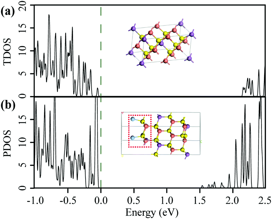 | ||
| Fig. 6 (a) The total density of states for the Cu3SbS4 phase and (b) the partial density of states for Cu3SbS4/Ag. Insets show the corresponding optimized crystal structures. The green dashed line stands for the Fermi level position. The red dotted line in (b) frames out the Ag cluster and adjacent bilayer of Cu3SbS4. | ||
5. Conclusion
To improve all-around performance in thin-film solar cells, we have demonstrated hollow Cu3SbS4@Ag spheres composed of mutually bonded nanoparticles. A remarkably enhanced absorption over 2 × 105 cm−1 covering UV and visible regions and electrical resistivity of 0.08 Ω cm could be obtained from the synergistic effect of hollow structural features and surface plasmon resonance of Ag clusters. The bandgap energy was calculated theoretically for the Cu3SbS4/Ag system and a slight reduction of bandgap was observed. The detailed evolution process and self-driven breakage mechanism of hollow microspheres, and reinforcing way of noble metal were proposed in detail. Additionally, a facile one-pot solvothermal method was demonstrated to selectively synthesize four CAS nanocrystals of high purity and crystallinity and not only Cu3SbS4. The element Cu in Cu3SbS4 was in the form of Cu+ and not oxidized immediately after the synthesis, which allowed us to decorate the surface. The preparation mechanism and the reaction process of CAS phases was discussed in a chemistry way. It is believed that the detailed mechanism could guide the synthesis of most ternary sulfides and control their structural performance, as well as the optical, electrical and catalytic properties.Author contributions
Xiang Meng: conceptualization, data curation, writing – original draft; Xihao Chen: software, formal analysis, investigation; Jiang Cheng: methodology, visualization, resources; Fuqiang Zhai: formal analysis, resources; Wen Li: supervision, validation, writing – review & editing; Rui Hu: supervision, validation, writing – review & editing; Lu Li: supervision, validation, visualization; all authors have agreed to their individual contributions in this manuscript.Conflicts of interest
There are no conflicts to declare.Acknowledgements
This work was supported by the program of Public Service Platform for the Industrialization of Technological Innovation Achievements in the field of Robot and Intelligent Manufacturing in Chongqing (No. 2019-00900-1-1), the Science and Technology Research Program of Chongqing Municipal Education Commission Grant (No. KJQN201901324, KJQN201901348 and KJCX2020048) and Chongqing University of Arts and Sciences (P2018CL09).Notes and references
- T. D. Lee and A. U. Ebong, Renewable Sustainable Energy Rev., 2017, 70, 1286–1297 CrossRef CAS.
- L. Fu, J. Yu, J. Wang, F. Xie, S. Yao, Y. Zhang, J. Cheng and L. Li, Chem. Eng. J., 2020, 400, 125906 CrossRef CAS.
- R. Kamada, T. Yagioka, S. Adachi, A. Handa, K. F. Tai, T. Kato and H. Sugimoto, in 2016 IEEE 43rd Photovoltaic Specialists Conference (PVSC), IEEE, Portland, OR, USA, 2016, pp. 1287–1291 Search PubMed.
- W. K. Metzger, S. Grover, D. Lu, E. Colegrove, J. Moseley, C. L. Perkins, X. Li, R. Mallick, W. Zhang, R. Malik, J. Kephart, C.-S. Jiang, D. Kuciauskas, D. S. Albin, M. M. Al-Jassim, G. Xiong and M. Gloeckler, Nat. Energy, 2019, 4, 837–845 CrossRef CAS.
- F. Jiang, S. Ikeda, T. Harada and M. Matsumura, Adv. Energy Mater., 2014, 4, 1301381 CrossRef.
- K. Woo, Y. Kim and J. Moon, Energy Env. Sci., 2012, 5, 5340–5345 RSC.
- V. Steinmann, R. Chakraborty, P. H. Rekemeyer, K. Hartman, R. E. Brandt, A. Polizzotti, C. Yang, T. Moriarty, S. Gradečak, R. G. Gordon and T. Buonassisi, ACS Appl. Mater. Interfaces, 2016, 8, 22664–22670 CrossRef CAS.
- Y. Han, S. Siol, Q. Zhang and A. Zakutayev, Chem. Mater., 2017, 29, 8239–8248 CrossRef CAS.
- S. C. Riha, A. A. Koegel, J. D. Emery, M. J. Pellin and A. B. F. Martinson, ACS Appl. Mater. Interfaces, 2017, 9, 4667–4673 CrossRef CAS PubMed.
- C. Behera, R. Samal, C. S. Rout, R. S. Dhaka, G. Sahoo and S. L. Samal, Inorg. Chem., 2019, 58, 15291–15302 CrossRef CAS PubMed.
- G. H. Albuquerque, K.-J. Kim, J. I. Lopez, A. Devaraj, S. Manandhar, Y.-S. Liu, J. Guo, C.-H. Chang and G. S. Herman, J. Mater. Chem. A, 2018, 6, 8682–8692 RSC.
- L. Shi, C. Wu, J. Li and J. Ding, J. Alloys Compd., 2017, 694, 132–135 CrossRef CAS.
- G. Chen, W. Wang, J. Zhao, W. Yang, S. Chen, Z. Huang, R. Jian and H. Ruan, J. Alloys Compd., 2016, 679, 218–224 CrossRef CAS.
- B. Yang, L. Wang, J. Han, Y. Zhou, H. Song, S. Chen, J. Zhong, L. Lv, D. Niu and J. Tang, Chem. Mater., 2014, 26, 3135–3143 CrossRef CAS.
- W. Wang, M. T. Winkler, O. Gunawan, T. Gokmen, T. K. Todorov, Y. Zhu and D. B. Mitzi, Adv. Energy Mater., 2014, 4, 1301465 CrossRef.
- F.-H. Sun, J. Dong, H. Tang, P.-P. Shang, H.-L. Zhuang, H. Hu, C.-F. Wu, Y. Pan and J.-F. Li, Nano Energy, 2019, 57, 835–841 CrossRef CAS.
- X. Lu, D. T. Morelli, Y. Wang, W. Lai, Y. Xia and V. Ozolins, Chem. Mater., 2016, 28, 1781–1786 CrossRef CAS.
- Q. Zeng, Y. Di, C. Huang, K. Sun, Y. Zhao, H. Xie, D. Niu, L. Jiang, X. Hao, Y. Lai and F. Liu, J. Mater. Chem. C, 2018, 6, 7989–7993 RSC.
- J. van Embden, K. Latham, N. W. Duffy and Y. Tachibana, J. Am. Chem. Soc., 2013, 135, 11562–11571 CrossRef CAS.
- N. D. Franzer, N. R. Paudel, C. Xiao and Y. Yan, in 2014 IEEE 40th Photovoltaic Specialist Conference (PVSC), IEEE, Denver, CO, USA, 2014, pp. 2326–2328 Search PubMed.
- F. Zhang, K. Chen, X. Jiang, Y. Wang, Y. Ge, L. Wu, S. Xu, Q. Bao and H. Zhang, J. Mater. Chem. C, 2018, 6, 8977–8983 RSC.
- C. T. Crespo, J. Phys. Chem. C, 2016, 120, 7959–7965 CrossRef CAS.
- L. Zhou, Z. Zhuang, H. Zhao, M. Lin, D. Zhao and L. Mai, Adv. Mater., 2017, 29, 1602914 CrossRef PubMed.
- J. Wang, Y. Cui and D. Wang, Adv. Mater., 2019, 31, 1801993 CrossRef PubMed.
- M. Luo, Y. Liu, J. Hu, H. Liu and J. Li, ACS Appl. Mater. Interfaces, 2012, 4, 1813–1821 CrossRef CAS.
- L. Zhang, J. Colloid Interface Sci., 2018, 514, 396–406 CrossRef CAS PubMed.
- H. Sun, X. Zhang, F. Yan, H. Yuan, C. Zhu and Y. Chen, Appl. Surf. Sci., 2021, 554, 149238 CrossRef CAS.
- J. Wang, Y. Quan, G. Wang, D. Wang, J. Xiao, S. Gao, H. Xu, S. Liu and L. Cui, CrystEngComm, 2021, 23, 7385–7396 RSC.
- W. Zuo, L. Liang, F. Ye and S. Zhao, Chemosphere, 2021, 283, 131167 CrossRef CAS PubMed.
- G. Zhang, D. Chen, N. Li, Q. Xu, H. Li, J. He and J. Lu, Angew. Chem., 2020, 132, 8332–8338 CrossRef.
- W.-N. Wang, C.-Y. Zhang, B.-J. Chen, Z.-Y. Chu, Z.-B. Zha and H.-S. Qian, Appl. Surf. Sci., 2020, 515, 146130 CrossRef CAS.
- X. Feng, Q. Jiao, H. Cui, M. Yin, Q. Li, Y. Zhao, H. Li, W. Zhou and C. Feng, ACS Appl. Mater. Interfaces, 2018, 10, 29521–29531 CrossRef CAS PubMed.
- L. Su, Y. Hu, Z. Ma, L. Miao, J. Zhou, Y. Ning, Z. Chang, B. Wu, M. Cao, R. Xia and J. Qian, Sol. Energy Mater. Sol. Cells, 2020, 210, 110484 CrossRef CAS.
- T. Duan, W. Lou, X. Wang and Q. Xue, Colloids Surf., A, 2007, 310, 86–93 CrossRef CAS.
- Y.-H. Zhang, L. Guo, L. He, K. Liu, C. Chen, Q. Zhang and Z. Wu, Nanotechnology, 2007, 18, 485609 CrossRef.
- X. B. Cao, L. Gu, L. J. Zhuge, W. J. Gao, W. C. Wang and S. F. Wu, Adv. Funct. Mater., 2006, 16, 896–902 CrossRef CAS.
- S. Ding, X. Liu, Y. Shi, Y. Liu, T. Zhou, Z. Guo and J. Hu, ACS Appl. Mater. Interfaces, 2018, 10, 17911–17922 CrossRef CAS PubMed.
- Y. Wang, Q. Zhu, L. Tao and X. Su, J. Mater. Chem., 2011, 21, 9248 RSC.
- J. Yang, Y. Niu, J. Huang, L. Liu and X. Qian, Electrochim. Acta, 2020, 330, 135333 CrossRef CAS.
- B. Zhao, G. Shao, B. Fan, W. Zhao, Y. Xie and R. Zhang, J. Mater. Chem. A, 2015, 3, 10345–10352 RSC.
- Y. Sun, Nanoscale, 2010, 2, 1626 RSC.
- S. Saeed, H. Siddique, R. Dai, J. Wang, A. Ali, C. Gao, X. Tao, Z. Wang, Z. Ding and Z. Zhang, J. Phys. Chem. C, 2021, 125, 7542–7551 CrossRef CAS.
- W. Ren, Y. Yang, J. Yang, H. Duan, G. Zhao and Y. Liu, Chem. Eng. J., 2021, 415, 129052 CrossRef CAS.
- Z. Li, W. Huang, J. Liu, K. Lv and Q. Li, ACS Catal., 2021, 11, 8510–8520 CrossRef CAS.
- B. Vedhanarayanan, C.-C. Chen and T.-W. Lin, J. Power Sources, 2020, 477, 229033 CrossRef CAS.
- M. W. Knight, H. Sobhani, P. Nordlander and N. J. Halas, Science, 2011, 332, 702–704 CrossRef CAS PubMed.
- H. Li, Y. Hu, H. Wang, Q. Tao, Y. Zhu and Y. Yang, Sol. RRL, 2021, 5, 2000524 CrossRef CAS.
- N. Zhang, M. Li, C. F. Tan, C. K. Nuo Peh, T. C. Sum and G. W. Ho, J. Mater. Chem. A, 2017, 5, 21570–21578 RSC.
- W. Gao, Q. Liu, S. Zhang, Y. Yang, X. Zhang, H. Zhao, W. Qin, W. Zhou, X. Wang, H. Liu and Y. Sang, Nano Energy, 2020, 71, 104624 CrossRef CAS.
- P. Scherrer, Nachr. Ges. Wiss. Gottingn, 1918, 2, 89–93 Search PubMed.
- J. F. Moulder and J. Chastain, ed., Handbook of X-ray photoelectron spectroscopy: a reference book of standard spectra for identification and interpretation of XPS data, PerkinElmer Corporation, Eden Prairie, Minn, Update., 1992 Search PubMed.
- E. A. Davis and N. F. Mott, Philos. Mag., 1970, 22, 0903–0922 CrossRef CAS.
- G. Kresse and J. Furthmüller, Phys. Rev. B: Condens. Matter Mater. Phys., 1996, 54, 11169–11186 CrossRef CAS PubMed.
- J. P. Perdew and Y. Wang, Phys. Rev. B: Condens. Matter Mater. Phys., 1992, 46, 12947–12954 CrossRef PubMed.
- P. E. Blöchl, Phys. Rev. B: Condens. Matter Mater. Phys., 1994, 50, 17953–17979 CrossRef PubMed.
- K. Ramasamy, H. Sims, W. H. Butler and A. Gupta, Chem. Mater., 2014, 26, 2891–2899 CrossRef CAS.
- Q. Liang, K. Huang, X. Ren, W. Zhang, R. Xie and S. Feng, CrystEngComm, 2016, 18, 3703–3710 RSC.
- K. Chen, J. Zhou, W. Chen, Q. Chen, P. Zhou and Y. Liu, Nanoscale, 2016, 8, 5146–5152 RSC.
- C. An, Y. Jin, K. Tang and Y. Qian, J. Mater. Chem., 2003, 13, 301–303 RSC.
- V. K. Mariappan, K. Krishnamoorthy, P. Pazhamalai, S. Sahoo, S. S. Nardekar and S.-J. Kim, Nano Energy, 2019, 57, 307–316 CrossRef CAS.
- S. Yang, K. Liu, W. Han, L. Li, F. Wang, X. Zhou, H. Li and T. Zhai, Adv. Funct. Mater., 2020, 30, 1908382 CrossRef CAS.
- L. Wang, B. Yang, Z. Xia, M. Leng, Y. Zhou, D.-J. Xue, J. Zhong, L. Gao, H. Song and J. Tang, Sol. Energy Mater. Sol. Cells, 2016, 144, 33–39 CrossRef CAS.
- Q. Dong, Z. Jiao, H. Yu, J. Ye and Y. Bi, CrystEngComm, 2014, 16, 8317 RSC.
- P. Sinsermsuksakul, J. Heo, W. Noh, A. S. Hock and R. G. Gordon, Adv. Energy Mater., 2011, 1, 1116–1125 CrossRef CAS.
- P. A. Fernandes, A. Shongalova, A. F. da Cunha, J. P. Teixeira, J. P. Leitão, J. M. V. Cunha, S. Bose, P. M. P. Salomé and M. R. Correia, J. Alloys Compd., 2019, 797, 1359–1366 CrossRef CAS.
- E. Thouti, N. Chander, V. Dutta and V. K. Komarala, J. Opt., 2013, 15, 035005 CrossRef CAS.
- Ö. A. Yıldırım, H. E. Unalan and C. Durucan, J. Am. Ceram. Soc., 2013, 96, 766–773 CrossRef.
- C. A. Huerta-Aguilar, V. P. Barba, P. Thangarasu and R. T. Koodali, Chemosphere, 2018, 213, 481–497 CrossRef CAS PubMed.
- L. Yu, R. S. Kokenyesi, D. A. Keszler and A. Zunger, Adv. Energy Mater., 2013, 3, 43–48 CrossRef CAS.
- Q. Zhang, X. Ai, L. Wang, Y. Chang, W. Luo, W. Jiang and L. Chen, Adv. Funct. Mater., 2015, 25, 966–976 CrossRef CAS.
- F. Baum, T. Pretto, A. G. Brolo and M. J. L. Santos, Cryst. Growth Des., 2018, 18, 6521–6527 CrossRef CAS.
- U. V. Ghorpade, M. P. Suryawanshi, S. W. Shin, X. Wang, E. Jo, H. Bae, K. Park, J.-S. Ha, S. S. Kolekar and J. H. Kim, J. Mater. Chem. A, 2018, 6, 19798–19809 RSC.
- J. Cheng, Z. Dai, B. Chen, R. Ji, X. Yang, R. Hu, J. Zhu and L. Li, Nanoscale Res. Lett., 2016, 11, 550 CrossRef PubMed.
- J. van Embden and Y. Tachibana, J. Mater. Chem., 2012, 22, 11466 RSC.
- S. Ariponnammal, S. Chandrasekaran and C. Sanjeeviraja, Cryst. Res. Technol., 2012, 47, 145–150 CrossRef CAS.
- S. Li, Z. Wu, W. Li, Y. Liu, R. Zhuo, D. Yan, W. Jun and P. Yan, CrystEngComm, 2013, 15, 1571 RSC.
- X. Yu, J. Yu, B. Cheng and B. Huang, Chem. – Eur. J., 2009, 15, 6731–6739 CrossRef CAS PubMed.
- Y. Zhu, T. Liu, W. Ma, D. Zhang, N. Zhang, L. Chen, X. Liu and G. Qiu, Chem. Lett., 2015, 44, 1321–1323 CrossRef CAS.
- M. Aliofkhazraei, ed., Handbook of Nanoparticles, Springer International Publishing, Cham, 2016 Search PubMed.
- W. Ostwald, Z. Phys. Chem., 1900, 34U, 495–503 CrossRef.
- H. G. Yang and H. C. Zeng, J. Phys. Chem. B, 2004, 108, 3492–3495 CrossRef CAS.
- L. Shen, L. Lu, H. Wu, X.-Y. Yu, X. Zhang and X. W. Lou, Nat. Commun., 2015, 6, 1–8 Search PubMed.
- Y. Yin, C. K. Erdonmez, A. Cabot, S. Hughes and A. P. Alivisatos, Adv. Funct. Mater., 2006, 16, 1389–1399 CrossRef CAS.
- X. Cao, L. Gu, L. Zhuge, W. Qian, C. Zhao, X. Lan, W. Sheng and D. Yao, Colloids Surf., A, 2007, 297, 183–190 CrossRef CAS.
- T. A. Estrada-Mendoza, D. Willett and G. Chumanov, J. Phys. Chem. C, 2020, 124, 27024–27031 CrossRef CAS.
- J. Li, X. Han, J. Li, Y. Zhao and C. Fan, Phys. Status Solidi B, 2017, 254, 1600608 CrossRef.
- Y. Sun, Y. Wang, J. Y. C. Chen, K. Fujisawa, C. F. Holder, J. T. Miller, V. H. Crespi, M. Terrones and R. E. Schaak, Nat. Chem., 2020, 12, 284–293 CrossRef CAS PubMed.
- T. Shi, W.-J. Yin, M. Al-Jassim and Y. Yan, Appl. Phys. Lett., 2013, 103, 152105 CrossRef.
- K. Chen, C. Di Paola, B. Du, R. Zhang, S. Laricchia, N. Bonini, C. Weber, I. Abrahams, H. Yan and M. Reece, J. Mater. Chem. C, 2018, 6, 8546–8552 RSC.
- V. Bonačic-Koutecky, V. Veyret and R. Mitric, J. Chem. Phys., 2001, 115, 12 CrossRef.
Footnote |
| † Electronic supplementary information (ESI) available: XRD patterns and SEM images for Cu12Sb4S13, Cu3SbS3 and CuSbS2 phase by the solvothermal method; XPS spectra of as-synthesized Cu12Sb4S13 nanocrystals; Calculation method of Ag content from XRD results; EDS result of the as-synthesized Ag-coated Cu3SbS4 nanocrystals; XPS spectra of the as-synthesized Ag-coated Cu3SbS4 nanocrystal; UV–Vis–NIR spectra of Ag nanoparticles, Cu3SbS4 powder by melting method, Cu3SbS4 nanocrystals hollow spheres, 0.5 vol% Ag-coated Cu3SbS4 and 1 vol% Ag-coated Cu3SbS4, the corresponding Tauc plot of (αhν)1/2versus (hν) of the as-synthesized Cu3SbS4 nanocrystals hollow spheres and Ag-coated ones; XRD pattern of the as-synthesized bulk Cu3SbS4 by melting method; SEM images of the smaller spherical aggregation of crystals by only 5 min duration time at high temperature; The representative preparation method, structural properties and optical bandgap (indirect) of Cu3SbS4. See DOI: 10.1039/d1tc04098g |
| This journal is © The Royal Society of Chemistry 2022 |