DOI:
10.1039/D2TA04705E
(Paper)
J. Mater. Chem. A, 2022,
10, 21727-21737
Chain aggregation dictates bimolecular charge recombination and fill factor of all-polymer blend solar cells†
Received
13th June 2022
, Accepted 5th August 2022
First published on 30th September 2022
Abstract
One of the bottlenecks in improving power conversion efficiencies of all-polymer blend solar cells is the low fill factor (FF), along with the intolerance to film thickness. In this study, we examined the behavior of charge-carrier extraction and recombination to determine the key factors that improve or limit the FFs of all-polymer blend solar cells. We conducted space-charge-limited current mobility, electrical impedance spectroscopy, and grazing-incidence wide-angle X-ray scattering measurements for four exemplary all-polymer blend devices composed of a naphthalene diimide-based low-bandgap polymer acceptor. The high charge-carrier collection ability and, thus the high FF of ∼70% of the all-polymer blends result from the long charge-carrier lifetime due to small bimolecular recombination coefficients. The degree of suppression of the bimolecular charge recombination is quantified using the Langevin theory and is then related to the blend morphology of the device. Consequently, we conclude that the preferred blend morphology for suppressing bimolecular recombination is characterized by a well-ordered local structure due to chain aggregation by both the polymer donor and acceptor. This study guides future research efforts toward the development of thickness-tolerant all-polymer-blend solar cells with high FFs.
1. Introduction
Polymer:polymer blend (all-polymer blend) solar cells, which employ conjugated polymers as both electron-donating (donor) and electron-accepting (acceptor) semiconductors, have attracted attention owing to their excellent material properties such as high flexibility, favorable mechanical robustness as well as morphological stability, and superior solution processability.1–3 Compared with small-molecule-containing organic solar cells, all-polymer blend solar cells are considered the most promising candidates for solar cells that are suitable for cost-effective mass production because polymeric materials are compatible with printing fabrication owing to their readily tunable ink viscosity and ability to form uniform large-area films.
During the past decade, the emergence of naphthalene diimide (NDI)-based low-bandgap polymer acceptors with relatively high electron mobility has improved the power conversion efficiencies (PCEs) of all-polymer blend solar cells up to ∼11%.4 However, the state-of-the-art all-polymer blends employing NDI-based polymer acceptors are still lagging behind the solar cells constructed using fullerene and non-fullerene small-molecule acceptors. When the results from the all-polymer blends are considered, one of the bottlenecks in improving the PCE is the low fill factor (FF), which is typically <60% even in optimum devices. Presently, the active layer thickness for optimum performance is mostly limited to ∼100 nm, and thicker devices exhibit a drop in the FF and thereby PCE, with only a few exceptions.5 In contrast to the reported FF behavior of the all-polymer blends, many state-of-the-art fullerene-based blends achieve FFs of ≥70% in the optimum thin-film devices. Moreover, some devices maintain high FFs and their full performance when thick active layers (∼300 nm) are used.6–12 These thick-film devices are characterized by an increased absorption strength of the active layer and can consequently maximize the short-circuit current density (JSC) and PCE. Additionally, tolerance of the PCE to the film thickness is a prerequisite for fabricating solar cells via roll-to-roll or other high-volume printing techniques preferred for commercialization. Therefore, elucidating the intrinsic limitations that hinder the achievement of an excellent FF in all-polymer blend solar cells is essential not only for improving the device performance further but also for expanding their industrial application scope.
Recently, FFs of the solar cells constructed using fullerene and non-fullerene small-molecule acceptors have been correlated with the charge-carrier collection efficiency, which is determined by the competition between charge-carrier extraction and recombination.13–16 One of the benchmark polymer:fullerene solar cells that can maintain high FFs even with thick films is the blend of poly(3-hexylthiophene) (P3HT) and [6,6]-phenyl-C61-butyric acid methyl ester (PCBM).17,18 In the P3HT:PCBM device, the highly crystalline quality and purity of the P3HT aggregates facilitate the suppression of the bimolecular charge recombination because of the extended delocalization of the charge carriers.18 It is also suggested that, in terms of the charge-carrier extraction, both hole and electron mobilities of at least 10−4 cm2 V−1 s−1 are required to measure high FFs.19 Further, Li et al. reported that a high hole mobility (>1 × 10⁻³ cm2 V−1 s−1) comparable to the electron mobility of PCBM is required to guarantee efficient charge-carrier extraction, which increases the FF and sustains the high FF of ≥70% with a thick active layer of thickness >300 nm.12 Additionally, for the polymer:PCBM devices that employ less-crystalline polymer donors, weak PCBM percolation in a mixed region with the amorphous portions of the polymer donor inhibits efficient electron transport, thereby decreasing the FF of the thick-film devices.20,21 This bottleneck due to the weak percolation can be overcome by loading an excess of PCBM (∼80 wt%), with devices above 300 nm showing FF close to 60%.21
In contrast, our knowledge about the underlying factors that improve or limit the FF of all-polymer blend solar cells remains obscure because their morphological features are different from those of the polymer:PCBM blend systems. First, presently, efficient all-polymer blend solar cells have been developed by employing non-high crystalline polymers for both donor and acceptor. The most widely used donors are the polymers composed of 4,8-di(thiophen-2-yl)benzo[1,2-b:4,5-b′]-dithiophene (BDTT) unit into the backbone.3 Although the BDTT-based polymer donors can exhibit hole mobilities of ∼10−4 cm2 V−1 s−1, they are less- or moderate-crystalline.3,22 Therefore, long-range ordering with high crystalline quality, as observed for the P3HT aggregates, is difficult to realize.22,23 Second, the electron mobilities of the NDI-based polymer acceptors in blend films are typically lower than that of PCBM (>1 × 10⁻³ cm2 V−1 s−1).3 In contrast, the ability to allow percolation for charge transport in blend films is potentially higher for polymer acceptors than for small-molecule acceptors.24,25 Therefore, the loss of electron transport networks within the donor–acceptor mixed amorphous region may not necessarily become an intrinsic limitation of all-polymer blend solar cells.
With this background, in this study, we examined the behavior of charge-carrier extraction and recombination for all-polymer blend solar cells and compared the results with those of P3HT:PCBM blend solar cell to identify the key factors that dictate the FF of all-polymer blend systems. To this end, we conducted space-charge-limited current (SCLC) mobility measurements, electrical impedance spectroscopy (EIS), and grazing-incidence wide-angle X-ray scattering (GIWAXS) measurements for four exemplary all-polymer blend solar cells consisting of NDI-based polymer acceptors, N2200 and its fluorinated derivatives F-N2200, and two common BDTT-based polymer donors, PTB7-Th and PBDB-T.
2. Experimental
2.1 Materials
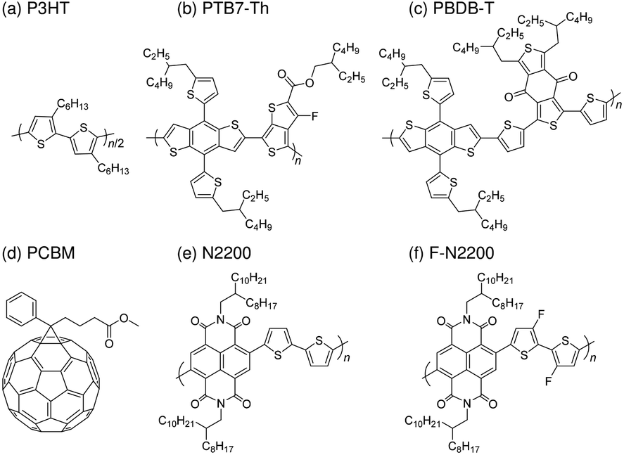
Poly[(2,6-(4,8-bis(5-(2-ethylhexyl)thiophen-2-yl)-benzo[1,2-b:4,5-b′]dithiophene))-alt-(5,5-(1′,3′-di-2-thienyl-5′,7′-bis(2-ethylhexyl)benzo[1′,2′-c:4′,5′-c′]dithiophene-4,8-dione)] (PBDB-T, 1-Material Inc.), poly[4,8-bis(5-(2-ethylhexyl)thiophen-2-yl)benzo[1,2-b;4,5-b′]dithiophene-2,6-diyl-alt-(4-(2-ethylhexyl)-3-fluorothieno[3,4-b]thiophene-)-2-carboxylate-2-6-diyl)] (PTB7-Th, 1-Material Inc.), and poly(3-hexylthiophene-2,5-diyl) (P3HT, head-to-tail regioregularity: 99.5%, Tokyo Chemical Industry Co., Ltd.) were used as the donor materials. Poly[[1,2,3,6,7,8-hexahydro-2,7-bis(2-octyldodecyl)-1,3,6,8-tetraoxobenzo[lmn][3,8]phenanthroline-4,9-diyl](3,3′-difluoro[2,2′-bithiophene]-5,5′-diyl)] (F-N2200, California Organic Semiconductors Inc.), poly{[N,N′-bis(2-octyldodecyl)naphthalene-1,4,5,8-bis(dicarboximide)-2,6-diyl]-alt-5,5′-(2,2′-bithiophene)} (N2200, California Organic Semiconductors Inc.), and [6,6]-phenyl-C61-butyric acid methyl ester (PCBM, Frontier Carbon Co.) were used as the acceptor materials. The chemical structures of the donors and acceptors are shown in Chart 1.
 |
| | Chart 1 Chemical structures of the donors (a) P3HT, (b) PTB7-Th, and (c) PBDB-T and acceptors (d) PCBM, (e) N2200, and (f) F-N2200 used in this study. | |
2.2 Device preparation and characterization
Polymer solar cells with an inverted architecture of ITO/ZnO/poly(ethylenimine) (PEI)|donor:acceptor blend|MoOx/Ag were fabricated. An indium tin oxide (ITO) substrate (GEOMATEC, Japan, 10 Ω per square) was sequentially washed via ultrasonication in toluene, acetone, and 2-propanol for 10 min, dried under an N2 flow, and treated with a UV-O3 cleaner (SSP16-110, SEN LIGHTS Corp., Japan) for 30 min. The ZnO electrode was prepared by spin coating a ZnO precursor solution on the precleaned ITO substrate.26 The ZnO precursor solution was prepared by dissolving zinc acetate dihydrate (50 mg, Sigma-Aldrich, 99.99%) and ethanolamine (14 μL, Sigma-Aldrich, ≥99.5%) in 500 μL of 2-methoxyethanol (Nacalai Tesque, 99%) under vigorous stirring for 12 h in air. The solution was spin-coated onto the ITO substrate at a spin rate of 4000 rpm for 60 s. The solution-coated ITO substrates were then annealed at 200 °C for 1 h in air. A PEI aqueous solution (Sigma-Aldrich, 50 wt% in H2O, Mw ∼750![[thin space (1/6-em)]](https://www.rsc.org/images/entities/char_2009.gif) 000 gmol−1) was diluted with 2-methoxyethanol to a weight concentration of 0.05 wt%, and the diluted PEI solution was subsequently spin-coated onto the ZnO electrode at a spin rate of 3000 rpm for 60 s, followed by annealing at 100 °C for 10 min in air. This PEI-coated ZnO electrode was used as a cathode.27 The solutions for the active layers were prepared by mixing the donor and acceptor in a 1:1 weight ratio in chlorobenzene for the PTB7-Th:N2200 and PTB7-Th:F-N2200 solutions, in chlorobenzene with 0.5 vol% (v/v) 1,8-diiodooctane (DIO) for the PBDB-T:N2200 and PBDB-T:F-N2200 solutions, and in o-dichlorobenzene for the P3HT:PCBM solution. The donor:acceptor blend solutions were stirred at 60 °C for at least 12 h to allow the complete dissolution of the materials. The solutions were then passed through a 0.45 μm filter and spin-coated onto the ZnO/PEI electrode. For the P3HT:PCBM blend film, the as-cast film was placed in a covered Petri dish for 1 h at room temperature (solvent annealing).28,29 The spin-coating solvents and DIO were selected according to the optimized recipe reported for the PTB7-Th:N2200,30 PBDB-T:N2200,31 and P3HT:PCBM29 blend solar cells. The active layer thickness was changed by varying the solution concentration and spin speed. The solution preparation and the subsequent spin-coating procedures were carried out in an N2-filled glove box. Finally, MoOx (10 nm) and Ag (100 nm) were sequentially vacuum deposited through a shadow mask at ∼8.0 × 10⁻⁵ Pa on top of the blend film to obtain a surface area of 0.04 cm2 for the MoOx/Ag top electrode, which was used as an anode. The current density–voltage (J–V) characteristics were measured using a computer-controlled Keithley 2401 source meter in an N2 atmosphere and under illumination with AM 1.5G-simulated solar light with a power density of 100 mW cm−2.
000 gmol−1) was diluted with 2-methoxyethanol to a weight concentration of 0.05 wt%, and the diluted PEI solution was subsequently spin-coated onto the ZnO electrode at a spin rate of 3000 rpm for 60 s, followed by annealing at 100 °C for 10 min in air. This PEI-coated ZnO electrode was used as a cathode.27 The solutions for the active layers were prepared by mixing the donor and acceptor in a 1:1 weight ratio in chlorobenzene for the PTB7-Th:N2200 and PTB7-Th:F-N2200 solutions, in chlorobenzene with 0.5 vol% (v/v) 1,8-diiodooctane (DIO) for the PBDB-T:N2200 and PBDB-T:F-N2200 solutions, and in o-dichlorobenzene for the P3HT:PCBM solution. The donor:acceptor blend solutions were stirred at 60 °C for at least 12 h to allow the complete dissolution of the materials. The solutions were then passed through a 0.45 μm filter and spin-coated onto the ZnO/PEI electrode. For the P3HT:PCBM blend film, the as-cast film was placed in a covered Petri dish for 1 h at room temperature (solvent annealing).28,29 The spin-coating solvents and DIO were selected according to the optimized recipe reported for the PTB7-Th:N2200,30 PBDB-T:N2200,31 and P3HT:PCBM29 blend solar cells. The active layer thickness was changed by varying the solution concentration and spin speed. The solution preparation and the subsequent spin-coating procedures were carried out in an N2-filled glove box. Finally, MoOx (10 nm) and Ag (100 nm) were sequentially vacuum deposited through a shadow mask at ∼8.0 × 10⁻⁵ Pa on top of the blend film to obtain a surface area of 0.04 cm2 for the MoOx/Ag top electrode, which was used as an anode. The current density–voltage (J–V) characteristics were measured using a computer-controlled Keithley 2401 source meter in an N2 atmosphere and under illumination with AM 1.5G-simulated solar light with a power density of 100 mW cm−2.
2.3 EIS measurements
Impedance measurements were conducted in an N2 atmosphere at room temperature using an Autolab PGSTAT204 system (Metrohm AG, Switzerland), equipped with a frequency analyzer module (FRA32M), at the frequency ranging from 1 MHz to 10 Hz. The AC oscillating amplitude was 10 mV (rms) to maintain the linearity of the response. A bias voltage, equal to the open-circuit voltage (VOC) obtained at each solar light intensity, was applied to perform measurements under zero-current conditions. The illumination intensities were changed from 1.6 to 100 mW cm−2 using neutral density filters.
2.4 Mobility measurements
For the hole mobility (μh) measurements, a hole-only device was fabricated using the following procedure. A 40 nm topcoat layer of poly(3,4-ethylenedioxythiophene):poly(4-styrenesulfonate) (PEDOT:PSS, H. C. Starck PH-500) was spin-coated onto a precleaned ITO substrate and then dried in air at 140 °C for 10 min. Next, a donor:acceptor blend solution was spin-coated onto the PEDOT:PSS-coated ITO substrate. Subsequently, Au (100 nm) or MoOx (10 nm) and Au (100 nm) were sequentially vacuum deposited on top of the blend film (ITO/PEDOT:PSS|donor:acceptor blend|Au or ITO/PEDOT:PSS|donor:acceptor blend|MoOx/Au). For the electron mobility (μe) measurements, an electron-only device was fabricated using the following procedure. Cesium carbonate (Cs2CO3; Sigma-Aldrich, 99.9%) was dissolved in 2-ethoxyethanol (Nacalai Tesque, ≥99.0%) to form a 0.2 wt% solution, which was then spin-coated on a precleaned ITO substrate at a spin rate of 1000 rpm for 60 s. The coated substrate was annealed at 170 °C for 20 min in an N2-filled glove box.32 Next, a donor:acceptor blend solution was spin-coated on the Cs2CO3-coated ITO electrode. Subsequently, Ca (10 nm) and Ag (100 nm) were sequentially vacuum deposited on top of the blend film (ITO/Cs2CO3|donor:acceptor blend|Ca/Ag). The spin-coating solvents, solvent annealing conditions, and donor:acceptor blend ratio were the same as those used to prepare each solar cell. The dark J–V characteristics were measured under an N2 atmosphere at room temperature. The charge-carrier mobility (μ) was calculated from the J–V characteristics by applying the SCLC method using the Mott–Gurney equation for the current density:  , where JSCLC is the current density, ε0 is the vacuum permittivity, εr is the dielectric constant of the film (assumed to be 3), and L is the thickness of the active layer.33,34
2.5 GIWAXS measurements
Neat films of the donor, acceptor, and donor:acceptor blends were prepared by spin coating the corresponding solutions onto a Si wafer (Yamanaka Hutech, Japan). The spin-coating solvents, solvent annealing conditions, and donor:acceptor blend ratio were the same as those used to prepare each solar cell. The GIWAXS measurement was performed on the films at room temperature at the SPring-8 BL40B2 beamline (Hyogo, Japan). The X-ray wavelength was set to 0.1 nm, and the beam impinged on the samples at an incident angle of 0.14° with respect to the sample surface. The X-ray exposure time was set to 50 s for all the samples. The scattering signals were detected by a hybrid photon-counting X-ray detector (Pilatus3 S 2M, Dectris Ltd., Switzerland) positioned at a distance of 343.3 mm from the sample in an area of 1475 × 1679 pixels. The scattering vector magnitude (q) expressed as q = (4π/λ)sinθ, where 2θ is the scattering angle, was calibrated using silver behenate (q = 2π/5.838 nm−1). A two-dimensional (2D) GIWAXS image was created by subtracting the diffraction pattern of the bare Si wafer from the total diffraction pattern of each film sample.
3. Results
3.1 Device performance
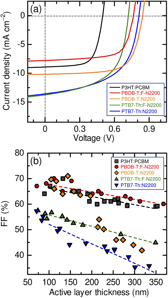
Fig. 1(a) shows the J–V characteristics of the all-polymer blend and the P3HT:PCBM blend solar cells. Table 1 summarizes the device performance parameters under white-light illumination with an intensity of 100 mW cm−2 (AM 1.5G). The devices were prepared under the optimal spin-coating conditions for each blend, as described in the Experimental section, and the active layer thickness (L) was adjusted to ∼100 nm. The optimum PTB7-Th:F-2200 and PTB7-Th:N2200 devices exhibited an FF of <60%, which is typical for all-polymer blend solar cells. In contrast, PBDB-T:F-N2200 and PBDB-T:N2200 devices achieved FF close to 70%, similar to that of the benchmark P3HT:PCBM solar ell. Additionally, significant differences in the FFs were apparent between the thick-film devices.
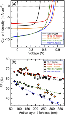 |
| | Fig. 1 (a) J–V characteristics of the devices under AM 1.5G (100 mW cm−2) illumination: P3HT:PCBM (103 nm, black), PBDB-T:F-N2200 (94 nm, red), PBDB-T:N2200 (117 nm, orange), PTB7-Th:F-N2200 (106 nm, green), and PTB7-Th:N2200 (86 nm, blue). (b) Dependence of the FF of each device on the active layer thickness: P3HT:PCBM (squares), PBDB-T:F-N2200 (circles), PBDB-T:N2200 (diamonds), PTB7-Th:F-N2200 (triangles), and PTB7-Th:N2200 (inverted triangles). | |
Table 1 Photovoltaic parameters, series resistance (RS), and shunt resistance (RSh) of the devices shown in Fig. 1a
| Device |
P3HT:PCBM |
PBDB-T:F-N2200 |
PBDB-T:N2200 |
PTB7-Th:F-N2200 |
PTB7-Th:N2200 |
|
R
S and RSh were obtained from the J–V characteristics under white-light illumination.
|
| Thickness (nm) |
103 |
94 |
117 |
106 |
86 |
|
J
SC (mA cm−2) |
8.9 |
7.8 |
10.2 |
13.8 |
13.6 |
|
V
OC (V) |
0.50 |
0.76 |
0.84 |
0.72 |
0.81 |
| FF (%) |
67 |
68 |
69 |
57 |
55 |
| PCE (%) |
3.0 |
4.1 |
5.9 |
5.6 |
6.1 |
|
R
S (Ω cm2)a |
7.0 |
7.5 |
6.1 |
5.1 |
6.4 |
|
R
Sh (Ω cm2)a |
1205 |
1282 |
2643 |
370 |
374 |
As shown in Fig. 1(b), the FFs of the PTB7-Th:F-N2200 and PTB7-Th:N2200 devices decreased with the increasing active layer thickness; the FFs were ∼50% (PTB7-Th:F-N2200) and ∼45% (PTB7-Th:N2200) at 200 nm thickness and further decreased to ∼45% (PTB7-Th:F-N2200) and ∼35% (PTB7-Th:N2200) at 350 nm thickness. In contrast, the FFs of the PBDB-T:F-N2200 and PBDB-T:N2200 devices were maintained at ∼65% at a thickness of 200 nm. Moreover, PBDB-T:F-N2200 device maintained a relatively high FF of 60%, even at a thickness of 350 nm. The high FF values and tolerance for the active layer thickness of the PBDB-T:F-N2200 device were comparable to those of the P3HT:PCBM device. The J–V characteristics of the thick devices are shown in Fig. S1 (ESI†). We note that the rapid FF drop observed for the >200 nm-thick PBDB-T:N2200 devices could be assigned to a space-charge-limited photocurrent because the device photocurrent was proportional to ∼V1/2 and ∼I3/4 (where I is the light intensity; Fig. S2, ESI†).35 The cause of the space-charge build-up could not be determined; however, further discussions on this aspect have been omitted as the topic was beyond the scope of this study.
3.2 Charge-carrier extraction and recombination
3.2.1 Charge-carrier mobilities of the blend films.
To study the charge-extraction ability of the blend films, we estimated the hole and electron mobilities through SCLC measurements. Fig. S3 in the ESI† shows the dark J–V curves of the hole-only and electron-only devices. Table 2 lists the resulting μh and μe values. The all-polymer blend films exhibited μh and μe values in the order of 10−4, and the values of the hole and electron mobilities were slightly imbalanced, as indicated by the mobility ratios in the range of 0.30–0.93. Using the mobilities, we evaluated the extraction time (τext) of the photogenerated charge carriers at the maximum power point (MPP) for the optimum thin-film devices. For the slightly imbalanced mobilities, the geometric average of the slower and faster carrier mobilities is proposed to favorably describe the extraction time.36,37 Therefore, the charge-carrier extraction time can be approximated as| |  | (1) |
where VMPP is the voltage at the MPP and| |  | (2) |
Table 2 Charge-carrier mobilities in the blend films and the estimated charge-carrier extraction times at the MPP of the optimum thin-film devices
| Device |
P3HT:PCBM |
PBDB-T:F-N2200 |
PBDB-T:N2200 |
PTB7-Th:F-N2200 |
PTB7-Th:N2200 |
|
Mobility ratio was defined as the ratio of the slower carrier mobility to the faster carrier mobility.
|
|
μ
h (cm2 V−1 s−1) |
5.34 × 10⁻⁴ |
5.09 × 10⁻⁴ |
3.99 × 10⁻⁴ |
8.28 × 10⁻⁴ |
5.72 × 10⁻⁴ |
|
μ
e (cm2 V−1 s−1) |
1.97 × 10⁻³ |
1.52 × 10⁻⁴ |
4.89 × 10⁻⁴ |
5.91 × 10⁻⁴ |
5.31 × 10⁻⁴ |
| Mobility ratioa |
0.27 |
0.30 |
0.82 |
0.71 |
0.93 |
|
τ
ext (s) |
0.61 × 10⁻⁶ |
1.34 × 10⁻⁶ |
0.80 × 10⁻⁶ |
0.45 × 10⁻⁶ |
0.32 × 10⁻⁶ |
As shown in Table 2, the all-polymer blend solar cells were not inferior to the P3HT:PCBM blend solar cell in the charge-carrier extraction times. Moreover, the PBDB-T:F-N2200 and PBDB-T:N2200 devices achieved higher FFs than those of the PTB7-Th:F-N2200 and PTB7-Th:N2200 devices without requiring a shorter τext. In other words, the FFs of these all-polymer blend solar cells are not controlled by the charge-carrier mobilities of the blend films.
3.2.2 Charge-carrier recombination.
To study the charge recombination, we performed EIS measurements on the all-polymer blends and P3HT:PCBM blend-based optimum thin-film devices. The EIS results obtained at different illumination intensities are shown in Fig. S4 in the ESI.† As shown in Fig. 2(a), the impedance spectra were characterized by a major RC arc with additional minor features observed at higher frequencies, similar to the rsults of previous reports.38,39 The low-frequency major arc is attributed to the process of photogenerated charge-carrier recombination (resistance Rrec) and storage (chemical capacitance Cμ) in the donor:acceptor blend film.38 This major arc defines a time constant, which is interpreted as the charge-carrier lifetime, expressed as RrecCμ.38,39 An equivalent electrical circuit used to model our EIS spectra is illustrated in Fig. 2(a).40 In the equivalent circuit, the low-frequency major arc is modeled as Rrec‖CPE. Here, a constant phase element (CPE), instead of Cμ, was used to obtain a better fitting.40,41 The high-frequency minor arc is represented by the Rbulk‖Cbulk combination and is attributed to the bulk resistance and capacitance that includes a geometric component in the donor:acceptor blend film. RS is the series resistance considering all components, such as metallic contact and wires. The Rrec‖CPE combination has an impedance ZCPE of| |  | (3) |
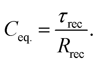
where QCPE is the magnitude of the CPE, and p represents an “ideality” factor characteristic of the distribution of the relaxation times. The value of p = 1 corresponds to an ideal capacitor. The average of the distribution of charge-carrier lifetimes (τrec) is given byand then, the CPE has an equivalent capacitance Ceq. of| |  | (5) |
 |
| | Fig. 2 (a) An example of the impedance spectra under the open-circuit condition and an equivalent electrical circuit for the devices. (b) Charge-carrier lifetime (τrec) as a function of VOC at different illumination intensities. (c) FF versus τrec under 1 sun irradiation conditions. Different symbols in the graphs (b) and (c) represent the results of different devices, as indicated by the legends in (c): P3HT:PCBM (squares), PBDB-T:F-N2200 (circles), PBDB-T:N2200 (diamonds), PTB7-Th:F-N2200 (triangles), and PTB7-Th:N2200 (inverted triangles). | |
Following this procedure, we calculated the τrec and Ceq. values. Fig. 2(b) shows τrec as a function of VOC under different illumination conditions for the all-polymer blend and P3HT:PCBM devices. For all devices, the τrec values vary almost exponentially with VOC, which is in good agreement with the previous results on polymer:fullerene devices.38,39,42,43 We extracted the τrec values under 1 sun irradiation conditions, obtaining 2.28 μs (P3HT:PCBM), 1.59 μs (PBDB-T:F-N2200), 1.11 μs (PBDB-T:N2200), 0.314 μs (PTB7-Th:F-N2200), and 0.263 μs (PTB7-Th:N2200) as the results. It is clear that the charge-carrier lifetimes in the PBDB-T donor-based devices are similar to the lifetime in the P3HT:PCBM device, whereas the lifetimes in the PTB7-Th donor-based devices are one-tenth times shorter than the lifetime in the P3HT:PCBM device. As shown in Fig. 2(c), the difference in the τrec values is correlated with the device FFs. Devices with τrec values as long as the value of P3HT:PCBM can achieve an FF close to 70%. In contrast, the devices with shorter τrec values showed an FF lower than 60%.
To explore the charge-carrier recombination mechanism, we determined the relationship between τrec and the charge-carrier density. The steady-state charge-carrier density (n) in the device under open-circuit conditions was calculated by integrating capacitance Ceq. over open-circuit voltages as follows:
| |  | (6) |
where
e is the elementary charge. Here, we calculated
n as the integral of the exponential fits, in which only the
Ceq. values at relatively high
VOCs are considered for fitting (solid lines fitted to the closed data in
Fig. 3(a)), over the range from 0 to
VOC,
| |  | (7) |
instead of the integral of the experimental values of the measured
Ceq.
44,45 The
τrec as a function of
n is illustrated in
Fig. 3(b). The analysis of the recombination mechanism is based on the bimolecular law for the relaxation of the photogenerated charge carriers, which is defined as
| |  | (8) |
where
krec(
n) is the carrier-density-dependent recombination coefficient. Additionally, we assumed
ne =
np =
n, where
ne and
np correspond to the steady-state electron and hole densities, respectively. To derive the charge-carrier lifetime from
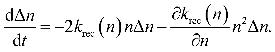
eqn (8), a small perturbation condition of the carriers, which was produced by the applied AC voltage in the EIS measurements, Δ
n ≪
n was applied, and
eqn (9) was obtained.
| |  | (9) |
 |
| | Fig. 3 (a) Capacitance Ceq. as a function of VOC at different illumination intensities. The solid lines represent the exponential fits, Ceq. = C0exp(αVOC), in which only the closed data were considered for fitting. (b) Charge-carrier lifetime as a function of the photogenerated charge-carrier density under open-circuit conditions. The broken lines are drawn only to guide the eye to show the slope −1. (c) Correlation of the charge-carrier lifetime with the bimolecular recombination coefficient under 1 sun irradiation conditions. Different symbols in the graphs (a)–(c) represent the results of the different devices, as indicated by the legends in (c): P3HT:PCBM (squares), PBDB-T:F-N2200 (circles), PBDB-T:N2200 (diamonds), PTB7-Th:F-N2200 (triangles), and PTB7-Th:N2200 (inverted triangles). | |
As the second summand has a minor weight, the charge-carrier lifetime τrec and the carrier density n are related by the following relationship:
| |  | (10) |
and its derivation is obtained from the previous studies performed by Garcia-Belmonte
et al.39 and Bisquert
et al.38,46,47Fig. 3(b) shows that
τrec ∝
n−1, indicating a bimolecular recombination with a constant, carrier-density-independent recombination coefficient,
krec. The values of
krec(
n) calculated using
eqn (10) are shown in Fig. S5 in the ESI.
† Such a bimolecular recombination coefficient that is nearly constant with respect to the carrier density has been observed in polymer:fullerene devices.
15,38,45 We extracted the
krec values under 1 sun irradiation conditions. The corresponding results were 1.04 × 10
−11 cm
3 s
−1 (P3HT:PCBM), 1.53 × 10
−11 cm
3 s
−1 (PBDB-T:F-N2200), 3.35 × 10
−11 cm
3 s
−1 (PBDB-T:N2200), 4.90 × 10
−10 cm
3 s
−1 (PTB7-Th:F-N2200), and 5.54 × 10
−10 cm
3 s
−1 (PTB7-Th:N2200). In
Fig. 3(c),
τrec is plotted against the
krec of each device, indicating that the longer charge-carrier lifetime is achieved
via a small bimolecular recombination coefficient.
It has been known that the dependence of VOC on the incident light intensity can qualitatively yield the dominant types of charge recombination.48–51 The VOCversus light intensity results for the devices are shown in Fig. S6 in the ESI.† The slopes of the plots for the different devices were 1.17kBT/e (PBDB-T:F-N2200), 1.07kBT/e (PBDB-T:N2200), and 1.18kBT/e (PTB7-Th:N2200), where kB is Boltzmann constant and T is the temperature in Kelvin. The slopes close to kBT/e indicate that bimolecular recombination dominates at the open circuit in the devices of PBDB-T:F-N2200, PBDB-T:N2200, and PTB7-Th:N2200.48,50,51 Additionally, the slopes were 1.24kBT/e and 1.38kBT/e for the P3HT:PCBM and PTB7-Th:F-N2200 devices, respctively. The stronger dependence of the VOC on the light intensity may indicate that the recombination at the open circuit is a combination of bimolecular and monomolecular (Shockley–Read–Hall) processes50,51 or that the slope is misleadingly increased due to the parasitic leakage current in the devices of P3HT:PCBM and PTB7-Th:F-N2200.49,50
3.2.3 Charge-carrier collection.
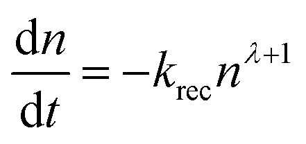
We considered the overall charge-carrier collection ability, which was determined by the competition between the charge-carrier extraction and recombination. Here, we should note that the small perturbation lifetimes τrec given by the EIS analysis must be multiplied by a factor of (λ + 1) to obtain the total charge-carrier lifetime τoverallrec in the device52,53| | | τoverallrec = (λ + 1)τrec, | (11) |
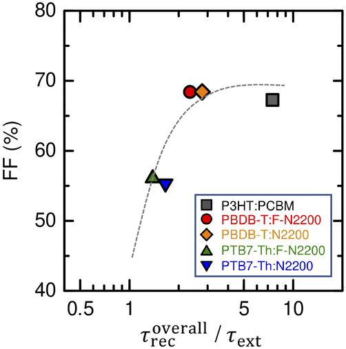
where λ is the slope in the power law relationship τrec ∝ n−λ determined from Fig. 3(b) and is related to the reaction order as  . As already stated, the devices fabricated in this study were characterized by λ = 1. Therefore, the lifetime of the total charge carriers in the device was evaluated as τoverallrec = 2τrec. Fig. 4 shows the FF versus τoverallrec/τext plot under 1 sun irradiation conditions, demonstrating that the devices with τoverallrec/τext > 2 (PBDB-T:F-N2200 and PBDB-T:N2200) achieved FF values of ∼70%, which are as high as that achieved by the P3HT:PCBM device. A τoverallrec/τext value greater than 2 indicates that the charge carriers can arrive at each electrode before recombination. Several of similar figures of merit have been introduced to be correlated with the FFs of the polymer:fullerene and polymer:non-fullerene small-molecule blend solar cells.13,15,16,18 Notably, the observed high charge-carrier collection ability of these devices results from the longer charge-carrier lifetimes due to the low bimolecular recombination coefficients and not the short charge-carrier extraction times.
 |
| | Fig. 4 FF versus τoverallrec/τext of the all-polymer blends and P3HT:PCBM blend solar cells. The dashed lines are drawn only to guide the eye. Different symbols represent the results of different devices as indicated by the legends in the graph. | |
3.3 Polymer chain ordering in films
To examine the molecular ordering of the polymer donor and acceptor, 2D GIWAXS measurements were performed on all the individual polymer neat films and their blended films. In each 2D GIWAXS pattern, the out-of-plane and in-plane 1D diffraction profiles were constructed by integrating the intensity at each q value over the azimuthal angle ranges of 85–95° and 5–15°, respectively. The d spacing related to chain stacking was calculated from the central position q of the Lorentzian-shaped fitted peaks, according to the following relationship:| |  | (12) |
The coherence length (Lc) was estimated from the full width at half maximum (FWHM) using the Scherrer equation (eqn (13)). The FWHM was determined from the fit, and the shape factor, K, was assumed to be 0.9.54,55
| |  | (13) |
The number of stacking layers (N) was characterized by the ratio of the coherence length to the stacking distance for a certain diffraction peak22 as
| |  | (14) |
The values obtained are summarized in Tables S1–S3 (ESI†).
First, we present the results for the neat films. The GIWAXS 2D pattern of P3HT shows distinctive (100), (200), and (300) lamellar peaks observed in the out-of-plane direction, and a well-defined π–π stacking peak (010) in the in-plane direction at qz = 16.56 nm−1, corresponding to a d spacing of 0.38 nm (Fig. S7 in the ESI†). The presence of the higher-order (h00) peaks indicates good molecular order in the alkyl-chain stacking direction. The Lc of the P3HT (010) peak is 4.71 nm, which is approximately 12 stacking layers in the π–π stacking, exhibiting a long-range order in this direction. The crystalline characteristic of P3HT observed in the neat film was retained in the blended film with PCBM (Fig. S7 and Table S1 in the ESI†). Fig. 5(a) and (b) show the 2D patterns of the neat films of the polymer donors. The PTB7-Th and PBDB-T films show well-defined (010) reflections arising from the π–π stacking in the out-of-plane direction. Additionally, the corresponding (100) reflection from the lamellar stacking is located exclusively in the in-plane direction for PTB7-Th, and it exhibits a diffused ring for PBDB-T. The 2D patterns indicate that the ordered fraction of the PTB7-Th chains is face-on, and that of PBDB-T tends to be face-on relative to the substrate. As shown by the 1D profiles (Fig. 5(c) and (d)), the most noteworthy difference between the two donors was the degree of chain ordering. From the in-plane (100) peak, lamellar stacking distance d100 and coherence length L100 of PTB7-Th (qxy = 2.68 nm−1) were calculated as 2.35 and 5.97 nm, and those of PBDB-T (qxy = 2.97 nm−1) as 2.12 and 16.07 nm, respectively. Additionally, PBDB-T exhibits a peak at qxy = 6.54 nm−1, which is assigned to the (001) chain backbone repetition, with d001 = 0.96 nm and L001 = 8.75 nm.56 From the out-of-plane (010) peak, π–π stacking distance d010 and coherence length L010 of PTB7-Th (qz = 16.19 nm−1) were calculated as 0.39 and 1.50 nm, and those of PBDB-T (qz = 17.32 nm−1) as 0.36 and 2.32 nm, respectively. The estimated N values indicated that PBDB-T forms an ordered structure consisting of six to eight densely stacked chains in both the lamellar and π–π stacking directions, whereas PTB7-Th forms aggregates made by packing of only three to four chains. As to the neat films of the polymer acceptors, the 2D and 1D profiles indicate that both F-N2200 and N2200 form an ordered structure consisting of 9–11 stacked chains in both the lamellar and π–π stacking directions, with the ordered fraction being mainly face-on relative to the substrate (Fig. S8 and Table S2 in the ESI†). We note that the acceptor neat films processed with DIO showed (h00) lamellar stacking reflections in both in-plane and out-of-plane directions, indicating lamellar stacking of the polymer chains oriented both parallel and perpendicular to the substrate. Additionally, the number of stackings slightly decreased; N was then equal to 6–7 in the lamellar stacking direction and 8 in the π–π stacking direction (Fig. S9 and Table S2 in the ESI†). The obtained values of the π–π stacking distance d010 and the number of π–π stacking layers N010 are shown in Fig. 6.
 |
| | Fig. 5 2D GIWAXS patterns of the (a) PTB7-Th and (b) PBDB-T neat films. 1D profiles in the (c) in-plane and (d) out-of-plane directions, obtained from the PTB7-Th (black lines) and PBDB-T (red lines) 2D patterns. | |
 |
| | Fig. 6 Number of π–π stacking layers as obtained from the 1D diffraction profiles for every 2D GIWAXS pattern of the polymer donor and acceptor neat films. Open circles represent the results of the acceptor films processed with 0.5 wt% of DIO. | |
Next, we show the results for the donor:acceptor blend films and compare them with those of the corresponding neat films. The 2D patterns of the blend films (Fig. 7(a)–(d)) indicate that blending does not alter the preferred orientation of the constituent polymers from those of their neat films. Moreover, the 1D profiles with higher-order diffraction peaks (Fig. 7(e)–(l)) were well reconstructed, with a clear peak position and width, via the superposition of the profiles obtained from the individual polymer donor and acceptor neat films (Fig. S10 in the ESI†). The Lorentzian-shaped peak fitting results for the in-plane profiles quantitatively demonstrate a higher degree of chain ordering (i.e., shorter stacking distance and larger coherence length) of PBDB-T than that of PTB7-Th, and the well-ordered stacking structures of the polymer acceptors remain in the blend films (Table S3 in the ESI†). The retention of the preferential orientation and molecular ordering of the constituent polymers in their blend films has been reported for blends composed of two face-on polymers.60
 |
| | Fig. 7 2D GIWAXS patterns of the blend films: (a) PTB7-Th:F-N2200, (b) PTB7-Th:N2200, (c) PBDB-T:F-N2200, and (d) PBDB-T:N2200. In-plane and out-of-plane 1D profiles obtained from the 2D patterns of the blend films (black lines): (e) and (i) PTB7-Th:F-N2200, (f) and (j) PTB7-Th:N2200, (g) and (k) PBDB-T:F-N2200, and (h) and (I) PBDB-T:N2200. The 1D profiles obtained from the individual neat film of the constituent polymer donor and acceptor are shown by red and blue lines, respectively. Peaks were assigned according to the ref. 57 for PTB7-Th, ref. 56 for PBDB-T, and ref. 58 and 59 for F-N2200 and N2200. | |
4. Discussion
We examined the behavior of charge-carrier extraction and recombination for four exemplary all-polymer blend solar cells and compared the results with those of the P3HT:PCBM blend solar cell. The all-polymer blends behaved similarly with respect to charge-carrier mobility, and they were not inferior to the P3HT:PCBM blend in terms of the extraction time for the charge carriers. However, the blends differed significantly in terms of the bimolecular charge recombination coefficients. Consequently, the difference between the charge-carrier collection abilities of the all-polymer blend solar cells arises from the different charge-carrier lifetimes, which depend on the krec values. The PBDB-T:F-N2200 blend with the longest τrec (smallest krec) exhibited an excellent FF of ∼70% and tolerance to thickness variations similar to those of P3HT:PCBM, with 350-nm thick devices retaining FF close to 60%.
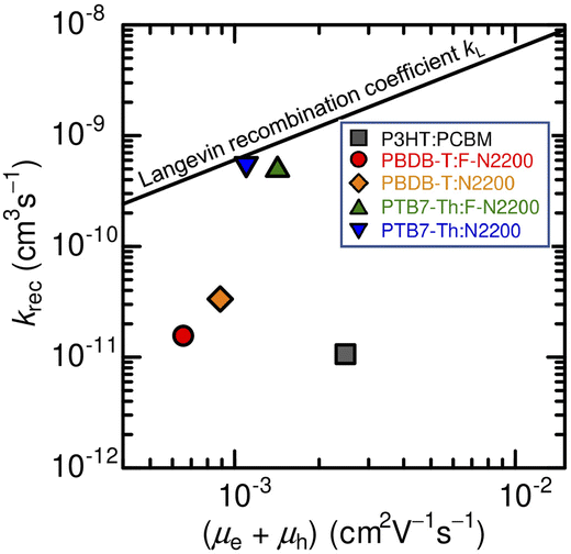
Here, we compare the experimentally determined rate constant krec with the Langevin recombination coefficient kL (see Fig. 8) given by eqn (15):61
| |  | (15) |
 |
| | Fig. 8 Bimolecular recombination coefficient krec determined by the EIS measurements compared with those calculated using the Langevin model expressed by eqn (15) (solid line). Different symbols represent the results of different devices as indicated by the legends in the graph. | |
As Langevin considered encounter-limited recombination of a free electron and a free hole in a homogeneous and isotropic medium, this expression represents the upper limit of the bimolecular recombination coefficient. Therefore, the degree to which the recombination is suppressed for the Langevin process is quantified by introducing the reduction factor, ξ, defined as62
| |  | (16) |
Fig. 8 shows that the degree of suppression of the bimolecular recombination in these all-polymer blend devices is dictated by the difference in the polymer donors (PTB7-Th and PBDB-T) rather than the acceptors (F-N2200 and N2200). The krec value for the PTB7-Th-based devices follows the Langevin description with ξ = 0.8 (PTB7-Th:N2200) and 0.6 (PTB7-Th:F-N2200). On the other hand, the krec value for the PBDB-T-based devices is reduced similarly to that of the P3HT:PCBM device, with ξ = 0.06 (PBDB-T:N2200), 0.04 (PBDB-T:F-N2200), and 0.007 (P3HT:PCBM). The small bimolecular recombination coefficient of the P3HT:PCBM blend, which is several orders of magnitude lower than that predicted by the Langevin model, has been widely observed.15,18 In contrast, suppressed bimolecular recombination has been reported in only a few all-polymer blend solar cells, such as P3HT:N2200 blends, to date.63 Our results on the PBDB-T-based devices demonstrate that the suppression of the bimolecular recombination is possible in the all-polymer blend solar cells, without the help of the high-crystalline nature of the polymer donors such as P3HT, and the densely aggregated PCBM networks with excellent electron mobilities (>1 × 10⁻³ cm2 V−1 s−1).
Previous studies on polymer:PCBM blends suggest that a more extended delocalization of the charge carriers leads to the suppression of bimolecular recombination, which may be achieved by the formation of polymer chain aggregates.18 For the NDI-based polymer acceptors, both F-N2200 and N2200 aggregated to form well-ordered local structures with N010 values in the range of 8–10. On the other hand, the polymer donors, PTB7-Th and PBDB-T, exhibited different chain ordering abilities. Along with the relatively larger N010, the d010 of PBDB-T (d010 = 0.36) was much shorter than that of PTB7-Th (d010 = 0.39) and was shorter than that of P3HT (d010 = 0.38). The short π–π stacking distance of PBDB-T suggests the formation of tight interchain packing structures that are favorable for charge delocalization within the aggregates. Considering that the chain ordering of the constituent polymer donor and acceptor remained even in the blend films, both electrons and holes are expected to be more delocalized in the devices employing PBDB-T than in those employing PTB7-Th. The low krec values of the PBDB-T-based devices suggest that charge delocalization in both the donor and acceptor aggregates is important for suppressing the bimolecular recombination in these all-polymer blend solar cells.
In terms of blend morphology, it is expected that chain aggregation of both polymer donor and acceptor drives the formation of a three-phase morphology composed of high-purity ordered donor and acceptor regions and a relatively more disordered intermixed region between them.64 Energetically, aggregation shifts the molecular orbitals such that the electronic gap is reduced compared to the disordered state.65,66 This creates an energy cascade that prevents the free carriers from approaching the donor/acceptor interface again from the aggregated chains within the donor and acceptor regions, which could mitigate encounter rates of a hole and electron.66,67 Furthermore, the networks consisting of the locally ordered and aggregated polymer chains may serve as excellent charge transport pathways due to their high local charge-carrier mobilities.68 The introduction of the locally well-ordered structure by chain aggregation of both polymer donor and acceptor, along with the resulting three-phase morphological features, will provide a guideline for mitigating bimolecular recombination and realizing the development of thick-film high-efficiency all-polymer blend solar cells.
5. Conclusion
In this study, we investigated the charge-carrier extraction and recombination in four exemplary all-polymer blend solar cells consisting of NDI-based polymer acceptors and BDTT-based polymer donors (PBDB-T:F-N2200, PBDB-T:N2200, PTB7-Th:F-N2200, and PTB7-Th:N2200) to determine the key factors that improve or limit FFs of all-polymer blend solar cells. The charge-carrier collection ability (τoverallrec/τext) > 2 and thus the high FFs of ∼70% exhibited by PBDB-T:F-N2200 and PBDB-T:N2200 blends were achieved because of the longer charge-carrier lifetimes due to the lower bimolecular recombination coefficients and not because of the shorter charge-carrier extraction times. The GIWAXS results indicated that an ordered local structure due to chain aggregation by both the polymer donor and acceptor is required for suppressing the bimolecular recombination in the all-polymer blend solar cells. The PBDB-T:F-N2200 device, featuring such a chain ordering, showed tolerance of FF to active layer thickness similar to that of P3HT:PCBM device, which performs well at thicknesses of 300 nm or more. Our results demonstrated that the suppression of bimolecular recombination is possible for all-polymer blend solar cells despite the absence of the high-crystalline nature of the polymer donors such as P3HT, and the densely aggregated PCBM networks with an excellent electron mobility in the order of 10−3 cm2 V−1 s−1. These results can guide us toward understanding the aspects that need attention in future studies related to the development of thick-film high-efficiency all-polymer blend solar cells.
Conflicts of interest
There are no conflicts to declare.
Acknowledgements
This work was supported by the Iwatani Naoji Foundation, Yazaki Memorial Foundation for Science and Technology, ENEOS Tonengeneral Research/Development Encouragement & Scholarship Foundation, and JSPS KAKENHI (Grant Number 19H02789). Synchrotron radiation experiments were performed at the SPring-8 BL40B2 beamline with the approval of the Japan Synchrotron Radiation Research Institute (JASRI) (Proposal No. 2020A1672).
Notes and references
- H. Benten, D. Mori, H. Ohkita and S. Ito, J. Mater. Chem. A, 2016, 4, 5340 RSC.
- G. Wang, F. S. Melkonyan, A. Facchetti and T. J. Marks, Angew. Chem., Int. Ed., 2019, 58, 4129 CrossRef CAS PubMed.
- C. Lee, S. Lee, G.-U. Kim, W. Lee and B. J. Kim, Chem. Rev., 2019, 119, 8028 CrossRef CAS.
- Z. Li, L. Ying, P. Zhu, W. Zhong, N. Li, F. Liu, F. Huang and Y. Cao, Energy Environ. Sci., 2019, 12, 157 RSC.
- B. Fan, W. Zhong, L. Ying, D. Zhang, M. Li, Y. Lin, R. Xia, F. Liu, H.-L. Yip, N. Li, Y. Ma, C. J. Brabec, F. Huang and Y. Cao, Nat. Commun., 2019, 10, 4100 CrossRef PubMed.
- C. Duan, F. Huang and Y. Cao, Polym. Chem., 2015, 6, 8081 RSC.
- V. Vohra, K. Kawashima, T. Kakara, T. Koganezawa, I. Osaka, K. Takimiya and H. Murata, Nat. Photonics, 2015, 9, 403 CrossRef CAS.
- Y. Liu, J. Zhao, Z. Li, C. Mu, W. Ma, H. Hu, K. Jiang, H. Lin, H. Ade and H. Yan, Nat. Commun., 2014, 5, 5293 CrossRef CAS PubMed.
- T. L. Nguyen, H. Choi, S.-J. Ko, M. A. Uddin, B. Walker, S. Yum, J.-E. Jeong, M. H. Yun, T. J. Shin, S. Hwang, J. Y. Kim and H. Y. Woo, Energy Environ. Sci., 2014, 7, 3040 RSC.
- W. Li, K. H. Hendriks, W. S. C. Roelofs, Y. Kim, M. M. Wienk and R. A. J. Janssen, Adv. Mater., 2013, 25, 3182 CrossRef CAS PubMed.
- X. Hu, C. Yi, M. Wang, C.-H. Hsu, S. Liu, K. Zhang, C. Zhong, F. Huang, X. Gong and Y. Cao, Adv. Energy Mater., 2014, 4, 1400378 CrossRef.
- W. Li, S. Albrecht, L. Yang, S. Roland, J. R. Tumbleston, T. McAfee, L. Yan, M. A. Kelly, H. Ade, D. Neher and W. Yu, J. Am. Chem. Soc., 2014, 136, 15566 CrossRef CAS PubMed.
- D. Bartesaghi, I. C. Pérez, J. Kniepert, S. Roland, M. Turbiez, D. Neher and L. J. A. Koster, Nat. Commun., 2015, 6, 7083 CrossRef CAS PubMed.
- D. Neher, J. Kniepert, A. Elimelech and L. J. A. Koster, Sci. Rep., 2016, 6, 24861 CrossRef CAS PubMed.
- M. C. Heiber, T. Okubo, S.-J. Ko, B. R. Luginbuhl, N. A. Ran, M. Wang, H. Wang, M. A. Uddin, H. Y. Woo, G. C. Bazan and T.-Q. Nguyen, Energy Environ. Sci., 2018, 11, 3019 RSC.
- N. Tokmoldin, J. Vollbrecht, S. M. Hosseini, B. Sun, L. Perdigón-Toro, H. Y. Woo, Y. Zou, D. Neher and S. Shoaee, Adv. Energy Mater., 2021, 11, 2100804 CrossRef CAS.
- J. A. Bartelt, D. Lam, T. M. Burke, S. M. Sweetnam and M. D. McGehee, Adv. Energy Mater., 2015, 5, 1500577 CrossRef.
- S. Wilken, D. Scheunemann, S. Dahlström, M. Nyman, J. Parisi and R. Österbacka, Adv. Electron. Mater., 2021, 7, 2001056 CrossRef CAS.
- C. M. Proctor, J. A. Love and T.-Q. Nguyen, Adv. Mater., 2014, 26, 5957 CrossRef CAS.
- J. A. Bartelt, Z. M. Beiley, E. T. Hoke, W. R. Mateker, J. D. Douglas, B. A. Collins, J. R. Tumbleston, K. R. Graham, A. Amassian, H. Ade, J. M. J. Fréchet, M. F. Toney and M. D. McGehee, Adv. Energy Mater., 2013, 3, 364 CrossRef CAS.
- S. Foster, F. Deledalle, A. Mitani, T. Kimura, K.-B. Kim, T. Okachi, T. Kirchartz, J. Oguma, K. Miyake, J. R. Durrant, S. Doi and J. Nelson, Adv. Energy Mater., 2014, 1400311 CrossRef.
-
Z. Peng, L. Ye and H. Ade, arXiv, 2020, preprint, arXiv:2005.13155, DOI:10.48550/arXiv.2005.13155.
- R. Noriega, J. Rivnay, K. Vandewal, F. P. V. Koch, N. Stingelin, P. Smith, M. F. Toney and A. Salleo, Nat. Mater., 2013, 12, 1038 CrossRef CAS.
- D. Mori, H. Benten, I. Okada, H. Ohkita and S. Ito, Adv. Energy Mater., 2014, 4, 1301006 CrossRef.
- Y. Zhang, Y. Xu, M. J. Ford, F. Li, J. Sun, X. Ling, Y. Wang, J. Gu, J. Yuan and W. Ma, Adv. Energy Mater., 2018, 8, 1800029 CrossRef.
- Y. Sun, J. H. Seo, C. J. Takacs, J. Seifter and A. J. Heeger, Adv. Mater., 2011, 23, 1679 CrossRef CAS.
- Y. Zhou, C. Fuentes-Hernandez, J. Shim, J. Meyer, A. J. Giordano, H. Li, P. Winget, T. Papadopoulos, H. Cheun, J. Kim, M. Fenoll, A. Dindar, W. Haske, E. Najafabadi, T. M. Khan, H. Sojoudi, S. Barlow, S. Graham, J.-L. Brédas, S. R. Marder, A. Kahn and B. Kippelen, Science, 2012, 336, 327 CrossRef CAS.
- G. Li, Y. Yao, H. Yang, V. Shrotriya, G. Yang and Y. Yang, Adv. Funct. Mater., 2007, 17, 1636 CrossRef CAS.
- S. Honda, H. Ohkita, H. Benten and S. Ito, Chem. Commun., 2010, 46, 6596 RSC.
- D. Mori, H. Benten, I. Okada, H. Ohkita and S. Ito, Energy Environ. Sci., 2014, 7, 2939 RSC.
- L. Ye, X. Jiao, W. Zhao, S. Zhang, H. Yao, S. Li, H. Ade and J. Hou, Chem. Mater., 2016, 28, 6178 CrossRef CAS.
- H.-H. Liao, L.-M. Chen, Z. Xu, G. Li and Y. Yang, Appl. Phys. Lett., 2008, 92, 173303 CrossRef.
- Y. Shen, A. R. Hosseini, M. H. Wong and G. G. Malliaras, ChemPhysChem, 2004, 5, 16 CrossRef CAS.
-
M. A. Lampert and P. Mark, Current Injection in Solids, Academic Press, New York, 1970 Search PubMed.
- V. D. Mihailetchi, J. Wildeman and P. W. M. Blom, Phys. Rev. Lett., 2005, 94, 126602 CrossRef CAS PubMed.
- S. Schiefer, B. Zimmermann and U. Würfel, J. Appl. Phys., 2014, 115, 044506 CrossRef.
- V. M. Le Corre, A. R. Chatri, N. Y. Doumon and L. J. A. Koster, Adv. Energy Mater., 2017, 7, 1701138 CrossRef.
- G. Garcia-Belmonte, P. P. Boix, J. Bisquert, M. Sessolo and H. J. Bolink, Sol. Energy Mater. Sol. Cells, 2010, 94, 366 CrossRef CAS.
- P. P. Boix, J. Ajuria, R. Pacios and G. Garcia-Belmonte, J. Appl. Phys., 2011, 109, 074514 CrossRef.
- B. J. Leever, C. A. Bailey, T. J. Marks, M. C. Hersam and M. F. Durstock, Adv. Energy Mater., 2012, 2, 120 CrossRef CAS.
- G. Perrier, R. Bettignies, S. Berson, N. Lemaître and S. Guillerez, Sol. Energy Mater. Sol. Cells, 2012, 101, 210 CrossRef CAS.
- G. Garcia-Belmonte, P. P. Boix, J. Bisquert, M. Lenes, H. J. Bolink, A. L. Rosa, S. Filippone and N. Martín, J. Phys. Chem. Lett., 2010, 1, 2566 CrossRef CAS.
- R. Casalini, S. W. Tsang, J. J. Deininger, F. A. Arroyave, J. R. Reynolds and F. So, J. Phys. Chem. C, 2013, 117, 13798 CrossRef CAS.
- G. Garcia-Belmonte, A. Guerrero and J. Bisquert, J. Phys. Chem. Lett., 2013, 4, 877 CrossRef PubMed.
- T. Ripolles-Sanchis, S. R. Raga, A. Guerrero, M. Welker, M. Turbiez, J. Bisquert and G. Garcia-Belmonte, J. Phys. Chem. C, 2013, 117, 8719 CrossRef CAS PubMed.
- A. Zaban, M. Greenshtein and J. Bisquert, ChemPhysChem, 2003, 4, 859 CrossRef CAS.
- J. Bisquert, F. Fabregat-Santiago, I. Mora-Seró, G. Garcia-Belmonte and S. Giménez, J. Phys. Chem. C, 2009, 113, 17278 CrossRef CAS.
- L. J. A. Koster, V. D. Mihailetchi, R. Ramaker and P. W. M. Blom, Appl. Phys. Lett., 2005, 86, 123509 CrossRef.
- C. M. Proctor and T.-Q. Nguyen, Appl. Phys. Lett., 2015, 106, 083301 CrossRef.
- C. M. Proctor, M. Kuik and T.-Q. Nguyen, Prog. Polym. Sci., 2013, 38, 1941 CrossRef CAS.
- S. R. Cowan, A. Roy and A. J. Heeger, Phys. Rev. B, 2010, 82, 245207 CrossRef.
- T. M. Clarke, C. Lungenschmied, J. Peet, N. Drolet and A. J. Mozer, Adv. Energy Mater., 2015, 5, 1401345 CrossRef.
- A. Maurano, C. G. Shuttle, R. Hamilton, A. M. Ballantyne, J. Nelson, W. Zhang, M. Heeney and J. R. Durrant, J. Phys. Chem. C, 2011, 115, 5947 CrossRef CAS.
- D.-M. Smilgies, J. Appl. Crystallogr., 2009, 42, 1030 CrossRef CAS PubMed.
- J. Rivnay, S. C. B. Mannsfeld, C. E. Miller, A. Salleo and M. F. Toney, Chem. Rev., 2012, 112, 5488 CrossRef CAS PubMed.
- L. Ye, X. Jiao, M. Zhou, S. Zhang, H. Yao, W. Zhao, A. Xia, H. Ade and J. Hou, Adv. Mater., 2015, 27, 6046 CrossRef CAS.
- J. Huang, J. Lee, J. Vollbrecht, V. V. Brus, A. L. Dixon, D. X. Cao, Z. Zhu, Z. Du, H. Wang, K. Cho, G. C. Bazan and T.-Q. Nguyen, Adv. Mater., 2020, 32, 1906027 CrossRef CAS PubMed.
- J. Rivnay, M. F. Toney, Y. Zheng, I. V. Kauvar, Z. Chen, V. Wagner, A. Facchetti and A. Salleo, Adv. Mater., 2010, 22, 4359 CrossRef CAS PubMed.
- J. Rivnay, R. Steyrleuthner, L. H. Jimison, A. Casadei, Z. Chen, M. F. Toney, A. Facchetti, D. Neher and A. Salleo, Macromolecules, 2011, 44, 5246 CrossRef CAS.
- Y. Yang, W. Chen, L. Dou, W.-H. Chang, H.-S. Duan, B. Bob, G. Li and Y. Yang, Nat. Photonics, 2015, 9, 190 CrossRef CAS.
- P. Langevin, Ann. Chim. Phys., 1903, 28, 433 Search PubMed.
- C. Göhler, A. Wagenpfahl and C. Deibel, Adv. Electron. Mater., 2018, 4, 1700505 CrossRef.
- S. Roland, M. Schubert, B. A. Collins, J. Kurpiers, Z. Chen, A. Facchetti, H. Ade and D. Neher, J. Phys. Chem. Lett., 2014, 5, 2815 CrossRef CAS.
- M. Osaka, H. Benten, H. Ohkita and S. Ito, Macromolecules, 2017, 50, 1618 CrossRef CAS.
- S. Sweetnam, K. R. Graham, G. O. N. Ndjawa, T. Heumüller, J. A. Bartelt, T. M. Burke, W. Li, W. You, A. Amassian and M. D. McGehee, J. Am. Chem. Soc., 2014, 136, 14078 CrossRef CAS PubMed.
- L. E. Garner, A. Bera, B. W. Larson, D. P. Ostrowski, A. J. Pal and W. A. Braunecker, ACS Energy Lett., 2017, 2, 1556 CrossRef CAS.
- S. Wilken, T. Upreti, A. Melianas, S. Dahlström, G. Persson, E. Olsson, R. Österbacka and M. Kemerink, Sol. RRL, 2020, 4, 2000029 CrossRef CAS.
- A. T. Hidayat, H. Benten, T. Kawanishi, N. Ohta, A. Muraoka and M. Nakamura, J. Phys. Chem. C, 2021, 125, 13741 CrossRef CAS.
Footnotes |
| † Electronic supplementary information (ESI) available. See https://doi.org/10.1039/d2ta04705e |
| ‡ Present address: Division of Materials Science, Faculty of Pure and Applied Sciences, University of Tsukuba, Ibaraki 305-8577, Japan. |
| § Present address: National Institute of Technology, Maizuru College, Kyoto 625-8511, Japan. |
|
| This journal is © The Royal Society of Chemistry 2022 |
Click here to see how this site uses Cookies. View our privacy policy here. 
 Open Access Article
 This Open Access Article is licensed under a Creative Commons Attribution-Non Commercial 3.0 Unported Licence
 *,
Yunju
Na
,
Zhiyuan
Liang
,
Naoki
Oyaizu
,
Junya
Suzuki
,
Shota
Kubota
,
Min-Cherl
Jung‡
*,
Yunju
Na
,
Zhiyuan
Liang
,
Naoki
Oyaizu
,
Junya
Suzuki
,
Shota
Kubota
,
Min-Cherl
Jung‡
 , where JSCLC is the current density, ε0 is the vacuum permittivity, εr is the dielectric constant of the film (assumed to be 3), and L is the thickness of the active layer.33,34


 . As already stated, the devices fabricated in this study were characterized by λ = 1. Therefore, the lifetime of the total charge carriers in the device was evaluated as τoverallrec = 2τrec. Fig. 4 shows the FF versus τoverallrec/τext plot under 1 sun irradiation conditions, demonstrating that the devices with τoverallrec/τext > 2 (PBDB-T:F-N2200 and PBDB-T:N2200) achieved FF values of ∼70%, which are as high as that achieved by the P3HT:PCBM device. A τoverallrec/τext value greater than 2 indicates that the charge carriers can arrive at each electrode before recombination. Several of similar figures of merit have been introduced to be correlated with the FFs of the polymer:fullerene and polymer:non-fullerene small-molecule blend solar cells.13,15,16,18 Notably, the observed high charge-carrier collection ability of these devices results from the longer charge-carrier lifetimes due to the low bimolecular recombination coefficients and not the short charge-carrier extraction times.