
On the role of surfaces and interfaces in electrochemical performance and long-term stability of nanostructured LSC thin film electrodes†
Katherine
Develos-Bagarinao
 *a,
Ozden
Celikbilek‡
b,
Riyan A.
Budiman
c,
Gwilherm
Kerherve
b,
Sarah
Fearn
b,
Stephen J.
Skinner
b and
Haruo
Kishimoto
a
*a,
Ozden
Celikbilek‡
b,
Riyan A.
Budiman
c,
Gwilherm
Kerherve
b,
Sarah
Fearn
b,
Stephen J.
Skinner
b and
Haruo
Kishimoto
a
aGlobal Zero Emission Research Center, National Institute of Advanced Industrial Science and Technology, AIST Tsukuba West, 16-1 Onogawa, Tsukuba, Ibaraki 305-8569, Japan. E-mail: develos-bagarinao@aist.go.jp
bDepartment of Materials, Imperial College London, Exhibition Road, London SW7 2AZ, UK
cResearch Institute for Energy Conservation, National Institute of Advanced Industrial Science and Technology, AIST Tsukuba Central 5, 1-1-1 Higashi, Tsukuba, Ibaraki 305-8565, Japan
First published on 1st November 2021
Abstract
Innovative concepts for novel electrode structures have been actively pursued over recent years to achieve both superior electrochemical performance as well as long-term stability for the development of solid oxide cells (SOCs) with efficient energy conversion. In this study, towards understanding the role of surfaces and interfaces on electrochemical performance and long-term stability of nanostructured La0.6Sr0.4CoO3−δ (LSC) thin film electrodes, a systematic investigation of the effect of deposition temperature and long-term annealing was conducted. The surface conditions of the LSC thin films, in terms of the proportion of surface-bound Sr and valence state of Co, are highly influenced by the deposition temperature; however, prolonged annealing at 700 °C in air of LSC thin films deposited at various temperatures essentially transforms their surfaces to a final state having similar chemical environment and crystalline properties. On the other hand, Sr diffusion across the LSC/GDC interfaces is promoted at higher deposition temperatures and is further accelerated with prolonged heating at 700 °C. Significant improvement in the electrochemical performance for symmetrical cells using LSC thin films is attributed to two main factors: enhancement of the surface exchange property as mediated by a distinctive nanostructure that allows the retention of a high porosity, and better stability of the electrode–electrolyte interfaces owing to the suppressed cation diffusion. This work paves the way to obtaining highly active and durable electrodes through tuning surfaces and interfaces and provides guidance for designing novel electrode materials with excellent performance for SOC applications.
Introduction
High performance and stability of electrode materials are crucial for the development of solid oxide cells (SOCs) towards efficient and sustainable energy conversion and storage.1–3 Lanthanum strontium cobalt perovskite oxide La0.6Sr0.4CoO3−δ (LSC), a mixed ionic and electronic conductor (MIEC), has been widely studied as a promising air electrode for cell operation at intermediate temperatures (500–700 °C) due to its high catalytic activity for oxygen reduction reaction (ORR).4–6 Due to its reactivity with state-of-the-art YSZ (yttria-stabilized zirconia) electrolyte, it is frequently used in conjunction with a rare-earth doped ceria such as GDC (gadolinia-doped ceria) which serves as a diffusion barrier layer or interlayer.6–9 However, using LSC as air electrode material in SOC cells and stacks is challenging due to the instability of its surfaces at the required operating temperatures, resulting in electrochemical performance degradation during long-term operation.10 Several studies have shown that strontium cobaltite surfaces like LSC are prone to Sr segregation and formation of Sr-rich phases, e.g., SrSO4 and SrCrO4, which result from a chemical reaction with trace impurities such as SO2 and Cr vapors contained in the supplied air or emanating from components in the system.10–13 A recent study has shown that the degradation on LSC surfaces already occurs from the first exposure to ambient air and measurement conditions, indicating the effect of environmental factors on electrode stability.14 Furthermore, it has been reported that the processing and thermal history affect the long-term stability of LSC due to surface restructuring and cation redistribution.15On the other hand, tuning the microstructure to nanoscaled LSC grains prepared by metalorganic deposition has provided very low polarization resistances16,17 at temperatures as low as 600 °C, although the stability of those structures with long-term testing has not been demonstrated. As has been observed for similar nanograined electrodes, coarsening due to granular sintering at high temperatures in air leads to rapid degradation in performance,18 at times even more accelerated than conventional micrometer-scaled electrodes. This behaviour is likely associated with the rapid cation diffusion along grain boundaries compared to the bulk, leading to enhanced cation segregation for nanoscaled LSC electrodes.19,20 In addition, recently a lot of interest has been focused on the development of thin film electrodes which are prepared at much lower temperatures using pulsed laser deposition (PLD). There are at least two primary motivations in this pursuit: first, it has been reported that the poorly crystalline structures are beneficial in driving the ORR activity in terms of suppressing the extensive segregation on LSC surfaces.21 Second, amorphous La0.8Sr0.2CoO3−δ films investigated using the isotope exchange depth profiling technique showed that the oxygen diffusion coefficient as well as surface exchange coefficient were higher compared to crystalline ones, even though no differences in the surface chemical composition were observed.22 Nevertheless, the LSC films investigated in these studies were prepared on single-crystal substrates which are not used for practical cells, and their adaptability for polycrystalline ceramic substrates has not yet been fully explored. Model electrodes or model diffusion couples provide simplified structures to gain important insights into the behaviour of surfaces and interfaces; however, it is necessary to examine the validity of these behaviours in systems and structures which approximate those of cells used in practical applications.
Taking into consideration the above issues, in this study we explore the effect of processing parameters, in particular, deposition at relatively low temperatures ranging between 500 °C and room temperature, and subsequent exposure to typical SOC operating temperatures with prolonged duration (at 700 °C up to 300 h), on the electrode performance and stability of nanostructured LSC thin films. Here we employ polycrystalline GDC as electrolyte substrates to gain a better understanding of the electrode–electrolyte interfacial behaviour and its evolution with long-term testing. The LSC films deposited on GDC are not epitaxial but are formed as nanostructured polycrystalline thin films. The nanostructured LSC thin films deposited at room temperature exhibited relatively lower values of electrode polarization resistance and less degradation compared to those prepared under higher deposition temperatures. Employing complementary and advanced characterization tools including X-ray photoelectron spectroscopy (XPS), secondary ion mass spectrometry (SIMS), and transmission electron microscopy (TEM), we examine in detail the surfaces and interfacial properties towards understanding their correlation to the performance and stability of nanostructured LSC thin films.
Experimental
Sample preparation
The LSC thin films were prepared using a PLD system (NanoPLD, PVD Products) equipped with a KrF excimer laser (wavelength: 248 nm, COMPex 102, Coherent) operated with the following parameters: 20 Hz repetition rate, 275 mJ laser energy, 100 mTorr oxygen background pressure, 53![[thin space (1/6-em)]](https://www.rsc.org/images/entities/char_2009.gif) 350 total pulses. The ceramic LSC target was prepared using commercial powders of nominal composition La0.6Sr0.4CoO3−δ (Noritake, Japan). The substrates were polished GDC (Ce0.9Gd0.1O1.95) pellets with a diameter of 20 mm and thickness of 0.5 mm. The deposition temperature was selected as 500 °C, 300 °C, and room temperature (R.T., no heating). After the deposition, the films were allowed to cool inside the chamber in the same ambient atmosphere from the set deposition temperature (i.e., 500 °C and 300 °C) to room temperature. The as-grown films were then simultaneously post-annealed in a box furnace at 700 °C for 300 h in air.
350 total pulses. The ceramic LSC target was prepared using commercial powders of nominal composition La0.6Sr0.4CoO3−δ (Noritake, Japan). The substrates were polished GDC (Ce0.9Gd0.1O1.95) pellets with a diameter of 20 mm and thickness of 0.5 mm. The deposition temperature was selected as 500 °C, 300 °C, and room temperature (R.T., no heating). After the deposition, the films were allowed to cool inside the chamber in the same ambient atmosphere from the set deposition temperature (i.e., 500 °C and 300 °C) to room temperature. The as-grown films were then simultaneously post-annealed in a box furnace at 700 °C for 300 h in air.
For the evaluation of the electrochemical performance, symmetrical cells comprised of LSC thin films deposited on both sides of GDC substrates pre-coated with LSCF (nominal composition: La0.6Sr0.4Co0.2Fe0.8O3−δ) thin films were used. With this configuration, the resulting electrode interface with the GDC electrolyte can therefore be assumed to be uniform for all the samples regardless of the microstructure of the LSC layer. The LSCF thin films were also prepared using PLD with the following parameters: 750 °C deposition temperature, 10 Hz repetition rate, 200 mJ laser energy, 35 mTorr oxygen background pressure, 60000 total pulses. Under these conditions, the obtained LSCF thin films have an average thickness of ∼270 nm. The electrode area is fixed at 0.785 cm2.
A detailed summary of the samples used in this study is shown in Table 1.
| Sample reference | Configuration | LSC deposition temperature | Annealing temperature/time | LSCF deposition temperature |
|---|---|---|---|---|
| A1 | LSC/GDC | 500 °C | — | — |
| B1 | LSC/GDC | 300 °C | — | — |
| C1 | LSC/GDC | R.T. | — | — |
| A2 | LSC/GDC | 500 °C | 700 °C/300 h | — |
| B2 | LSC/GDC | 300 °C | 700 °C/300 h | — |
| C2 | LSC/GDC | R.T. | 700 °C/300 h | — |
| A3 | LSC/LSCF/GDC/LSCF/LSC | 500 °C | 700 °C/300 h | 750 °C |
| B3 | LSC/LSCF/GDC/LSCF/LSC | 300 °C | 700 °C/300 h | 750 °C |
| C3 | LSC/LSCF/GDC/LSCF/LSC | R.T. | 700 °C/300 h | 750 °C |
Characterization
Cation depth profiles from the surface to the electrode/electrolyte interface were analyzed using time-of-flight SIMS (ToF-SIMS) on a ToF-SIMS5 machine (IONTOF GmbH, Münster, Germany) equipped with a bismuth liquid metal ion gun. A 25 keV Bi+ primary ion beam was used to generate secondary ions in the high current bunch mode and 10 keV argon cluster beam (Arn+) was used for the depth profiling. Positive secondary ion species of La+, Sr+ and Co+ from the film and Ce+, Gd+ from the electrolyte were monitored over an analysis area of 100 × 100 μm2 within a sputtering area of 300 × 300 μm2. The sputtered depths were calibrated using the film thickness measured using a scanning electron microscope (SEM, NovaNanoSEM450, FEI), used for both surface and cross-sectional observations in secondary and backscattered electron modes.The surface elemental composition and electronic structure were characterized using a ThermoFisher Scientific K-Alpha+ XPS system operating at 2 × 10⁻⁹ mbar base pressure at ambient temperature. The system incorporates a 180° double focusing hemispherical analyzer with a 128-channel detector. The Al Kα X-ray source generates a 6 mA emission current with a spot size of 400 μm2. Pass energies of 200 and 20 were used for the survey and core-level spectra, respectively. The quantitative analyses were performed using Avantage software.§ Shirley background function was applied and subtracted from the data. The peaks were fitted using a convolution of Gaussian and Lorentzian peak shapes. Sr 3d, La 3d, Co 2p, O 1s, and C 1s spectra were analyzed. The spectra were normalized to the total integrated intensity of the La 3d5/2 spectra. The binding energies were corrected to the C 1s peak position at 284.8 eV originating from surface hydrocarbons.
Specimens for TEM characterizations were prepared using a dual-beam plasma focused ion beam (PFIB)-SEM equipped with a Xe+ plasma source accelerated at a maximum voltage of 30 kV (ThermoFisher, Helios5 Hydra CX). Final thinning was performed at an acceleration voltage of 3 kV. Analytical measurements were performed using a TEM machine (FEI, Tecnai Osiris) equipped with energy dispersive X-ray spectroscopy (EDX) detector and operated at 200 kV acceleration voltage in scanning transmission electron microscopy (STEM) mode with a probe diameter of ∼0.3 nm.
AC impedance measurements
To ensure homogeneous contact with the PLD-grown LSC thin films, unsintered ∼10 μm-thick screen-printed layer of μm-scaled LSC particles were prepared by screen printing method. Gold mesh was pressed onto the screen-printed LSC as contact. Electrochemical impedance spectra were recorded with a Versastat4 (Princeton Applied Research, USA) frequency response analyzer in a frequency range of 10−2 Hz to 106 Hz at 700 °C in flowing air (compressed air with flow rate of 50 ml min−1) for ∼300 h. The impedance data obtained at open-circuit voltage condition were analyzed and fitted using the Zview software (version 3.5 h, Scribner and Associates, Inc.). To elucidate the different electrode reaction processes and confirm their physical origin, the impedance spectra were analyzed using distribution of relaxation times (DRT) method using Z-assist software (Toyo Corp., Japan). Further details have been reported in a previous publication.23Results and discussion
Microstructural characterization
Fig. 1 shows the typical plan-view and cross-sectional SEM images of the as-grown LSC thin films directly prepared on GDC electrolytes (samples A1, B1, and C1 in Table 1) at various deposition temperatures. For LSC deposited at 500 °C (Fig. 1(a)), the nanostructure features closely packed grains ranging from ∼10 to ∼20 nm in diameter, with distinct nanocolumnar structures spanning the thickness of the film (average thickness: ∼600 nm). This high-level ordering is attributed to the increased migration and diffusivity of the species resulting from the thermal heating. This type of nanostructure is typical of the films deposited under a high-temperature, low-oxygen pressure regime where nanocolumnar growth is promoted.24,25 Decreasing the deposition to 300 °C (Fig. 1(b)), we observe that the characteristic nanostructure became more porous in comparison to the one deposited at 500 °C, due to the formation of nanochannels throughout the film; the cross-sectional SEM image shown in Fig. 1(e) shows that its thickness (average thickness: ∼560 nm) is comparable to that of 500 °C. Lastly, the room-temperature LSC thin film (Fig. 1(c)) is characterized by a highly porous nanostructure due to the incorporation of relatively wider nanochannels in between granular clusters that at close inspection display fractal-like features. In particular, the film comprises slightly tilted branch-like features which are themselves composed of similarly structured branches, giving an overall appearance resembling fibers. There also seems to be a high degree of porosity inherent in the nanostructure, due to the loose packing of the branches. Despite the fact that this film was grown at room temperature only, the resulting morphology is indicative of a pseudo-ordered structure that is likely determined by the intrinsic kinetic energy of the arriving species generated from the laser plume during the PLD process. The average thickness of this sample is ∼1040 nm, almost twice as thick as the heated samples. This is accompanied by a significant increase in the overall film porosity.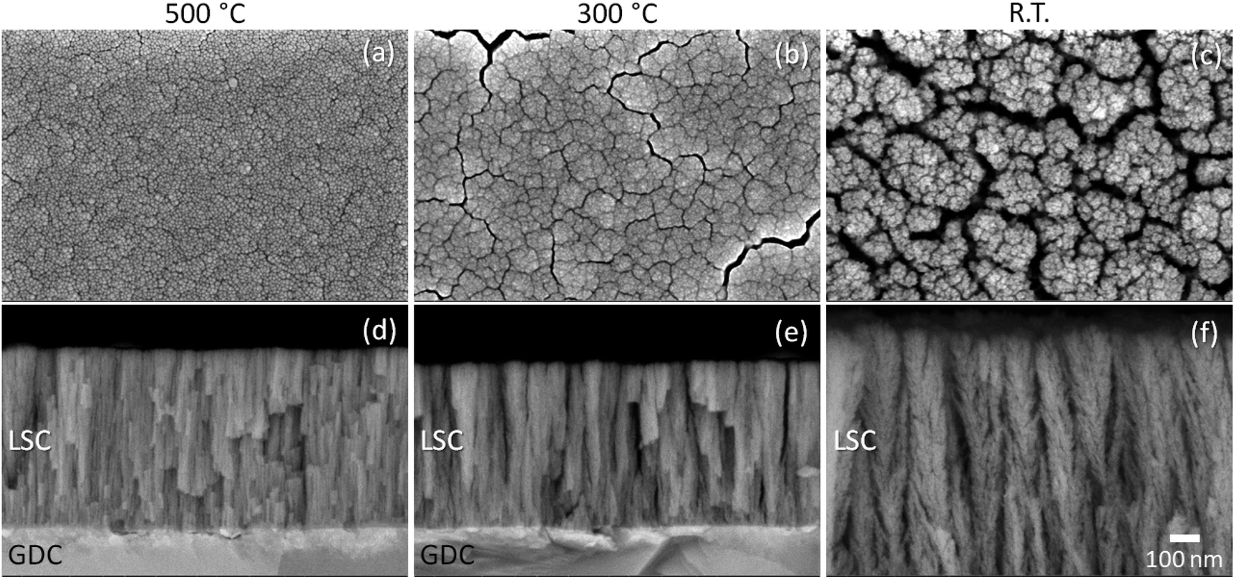 | ||
| Fig. 1 Typical plan-view SEM images of as-grown LSC films deposited at (a) 500 °C, (b) 300 °C, and (c) room temperature (R.T.). The film deposited at R.T. exhibits the highest porosity among the samples. The corresponding cross-sectional SEM images are shown in (d–f). The characteristic nanostructures vary widely depending on deposition temperature. The scale bar shown in image (f) corresponds to the scale of all images. | ||
Several studies have shown that nanostructured electrodes offer enhanced performance over conventional, micrometer-scaled ones due to catalytic effects associated with the nanoscaled structures, such as by promoting oxygen incorporation through grain boundary pathways, increased oxygen diffusivity through nanopores, space charge effects, etc.16,26–28 However, such nanostructured electrodes are usually beset by sintering behaviour at high temperatures which could drastically alter their initial morphologies and lead to electrochemical performance degradation in time. To gain more insights into this behaviour, the samples shown in Fig. 1 were subsequently annealed in air at 700 °C for 300 h, approximately resembling conditions for typical SOC operation (samples A2, B2, and C2 in Table 1). Fig. 2 shows the typical plan-view and cross-sectional SEM images of the LSC thin films after annealing. Analogous to the differences observed for the as-grown films, we also observe remarkable differences in the final nanostructures of the annealed films. Specifically, the 500 °C sample shows the densest nanostructure among the three as well as the lowest density of nanochannels (Fig. 2(a)). Unlike the other two samples, this sample shows mostly closed pores, suggesting that the film has densified extensively such that nanochannels which would have been through-thickness otherwise have formed into several closed nanopores (Fig. 2(d)). In contrast, we find that the R.T. sample (Fig. 2(c)) exhibits a drastic change from fractal-like structures to vertically clustered grains ranging in sizes from ∼50 nm to a few hundred nm, separated by wider nanochannels in between clusters. Interestingly, as can be viewed from the cross-section (Fig. 2(f)), the nanochannels conveniently provide open pores which would facilitate gas diffusion through the electrode layer, thus the resulting nanostructures present a much higher surface area which would be beneficial for the ORR process. Between these two samples, we can observe that the 300 °C sample (Fig. 2(b)) exhibits intermediate features; it has partially densified through the formation of clusters but with narrower nanochannels compared to those of the R.T. sample. Not all nanochannels are through-thickness pores, however. As shown in the cross-sectional SEM image (Fig. 2(e)), some pores only extend partly into the interior of the film, and some are closed.
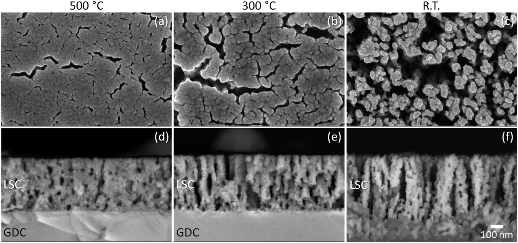 | ||
| Fig. 2 Typical plan-view SEM images of LSC films deposited at (a) 500 °C, (b) 300 °C, and (c) room temperature (R.T.), after annealing at 700 °C for 300 h in air. The corresponding cross-sectional SEM images are depicted in (d), (e), and (f). Extensive granular sintering can be observed, accompanied by an increase in overall porosities. Through-thickness nanochannels have formed in R.T. sample, whereas closed pores mostly formed in the 500 °C sample. The scale bar shown in image (f) corresponds to the scale of all images. | ||
These results suggest that the type of initial nanostructure strongly influences its evolution with annealing. For instance, the existence of finely dispersed nanochannels essentially limits the intergrain contact and thereby the extent of sintering to localized clusters, all the while maintaining a high porosity which would be beneficial for gas diffusion. In contrast, a highly dense nanocolumnar structure only tends to further densify with annealing. As we would show later, the unique formation of finely dispersed nanochannels is beneficial to improving the thermal stability of the thin film electrodes and achieve better electrochemical performance than those of relatively dense ones.
Surface characterization
Previous studies have shown that perovskite surfaces such as those of LSC are highly prone to the formation of Sr-rich phases, resulting in the deactivation of surfaces for ORR.29–36 To identify the cation chemistries with near-surface depth resolution, XPS analyses were performed on both as-grown and annealed LSC films.We first focus on the as-grown samples, with Sr 3d, O 1s, and C 1s core-level spectra displayed in Fig. 3 revealing different characteristics. The characteristic Sr 3d spectra consist of a doublet with 3d5/2 at lower binding energies (∼132 eV) corresponding to the lattice-bound Sr (Srlattice), and 3d3/2 at higher binding energies (∼133.5 eV) corresponding to surface-bound Sr (Srsurface). All as-grown samples exhibit a significant amount of Srsurface, however, the amount of lattice-bound Sr is the lowest for the R.T. sample, where it can be observed that the Srsurface intensity almost constitutes the majority of its total Sr signal. This implies that the R.T.-grown film contains a significant amount of Sr-rich phases on its surface compared to those of the other samples, which may be attributed to its lack of crystalline structure that will provide the chemical bonding states which would be normally found in an otherwise well-crystallized LSC lattice. Therefore, the so-called surface for the R.T. film mostly consists of randomly formed clusters emanating from the laser plume and may originate from Sr-rich species which could include SrO, Sr(OH)2, and SrCO3.
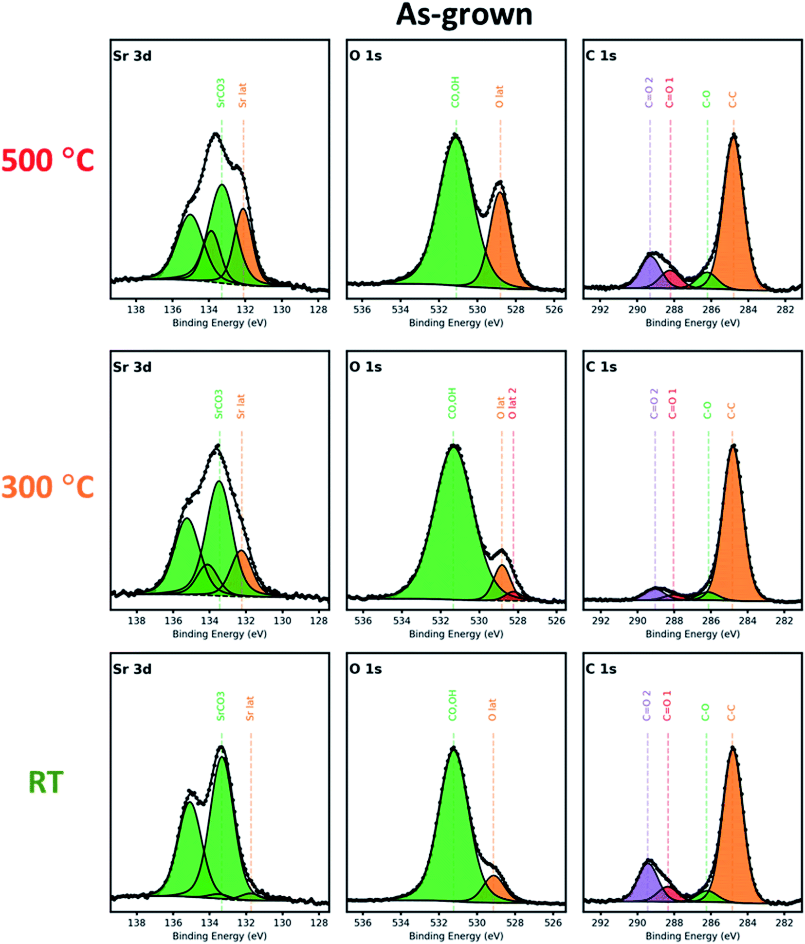 | ||
| Fig. 3 X-ray photoelectron spectra of Sr 3d, O 1s, and C 1s of the as-grown LSC nanostructured films grown at 500 °C, 300 °C, and R.T. | ||
Referring to the C 1s spectra, we can see the presence of a –CO3 binding environment in the spectra (∼289 eV), suggesting that the Srsurface likely originates mainly from SrCO3. This is evident for all as-grown samples. This is further corroborated by a relatively high amount of adsorbed oxygen species at the surface as evidenced by the peak at ∼531 eV of the O 1s spectra. Furthermore, it is observed that the peak at a lower binding energy of ∼529 eV which is associated with the metal–oxygen bonding in the crystal network becomes more prominent for higher deposition temperatures, which may be due to the removal of the unwanted phases on the surfaces with heating.
Turning our attention to the annealed samples shown in Fig. 4, it can be seen from the comparison of the Sr 3d spectra that the characteristic features are essentially the same: the Srlattice and Srsurface intensities are now comparable among the samples. This indicates that as-grown LSC films prepared at relatively low deposition temperatures mostly contain metastable surfaces which will invariably change into more stable ones upon annealing at higher temperatures.
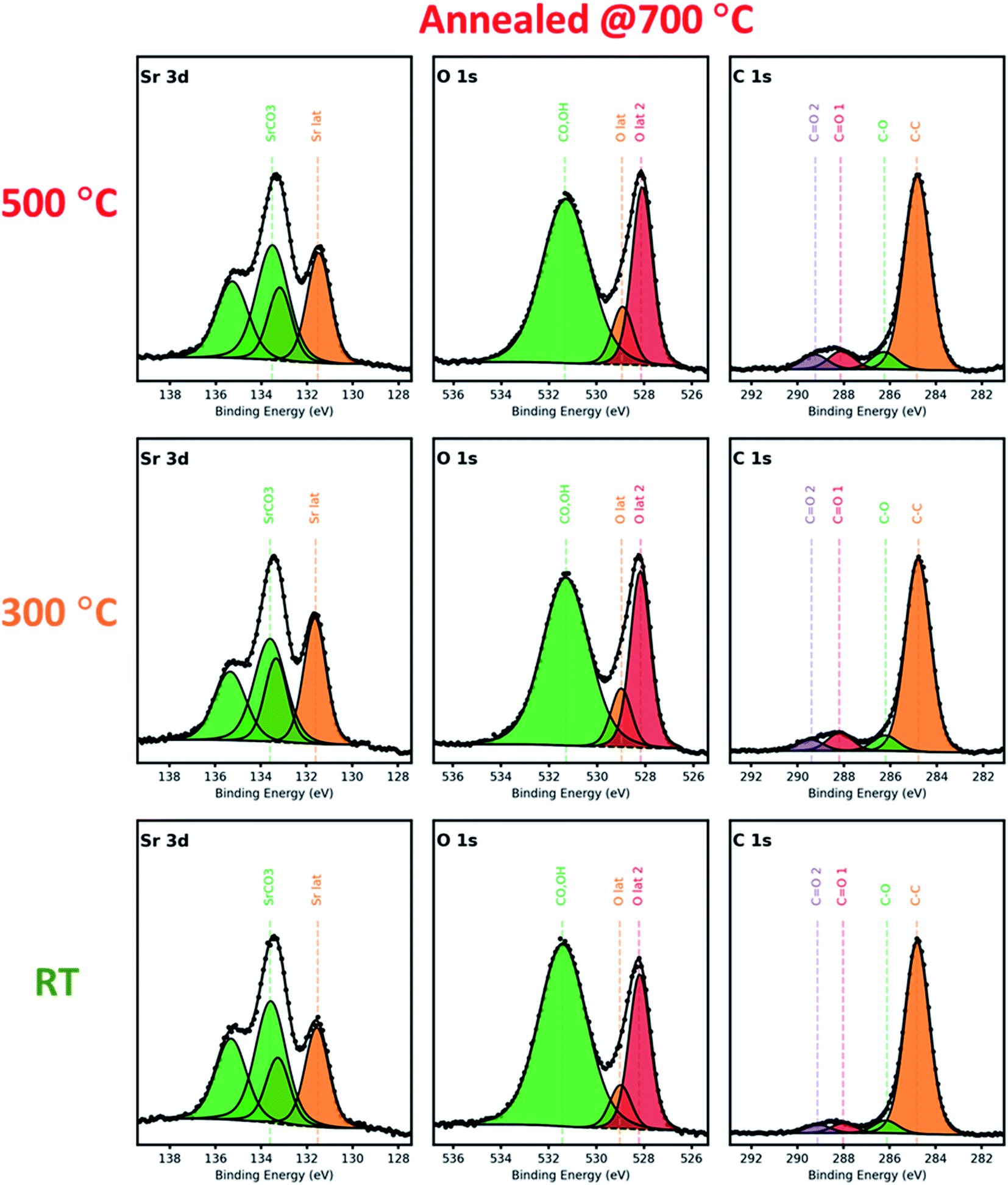 | ||
| Fig. 4 X-ray photoelectron spectra of Sr 3d, O 1s, and C 1s of the LSC nanostructured films grown at 500 °C, 300 °C, and R.T., after annealing at 700 °C for 300 h in air. | ||
Fig. 5 shows the comparison of the Co 2p core-level spectra of as-grown and annealed samples (additional X-ray photoelectron spectra of La 4d/3d, Sr 3d, Co 2p, and O 1s core-level spectra of the films are further presented in the ESI, Fig. S1†). The spectra show doublets of 2p1/2 and 2p3/2 and their satellite peaks, which help to identify the +2 and +3 oxidation states.21,37,38 The satellite peak at higher binding energy (∼789 eV) is attributed to mixed +2 and +3 oxidation states, while the satellite at the lower binding energy (∼786 eV) is assigned to only +2 oxidation state. All films showed a mixture of +2/+3 oxidation states, but the as-grown film prepared at R.T showed a higher amount of +2 oxidation state. After post annealing, the spectra once again resembled each other, suggesting that any initial differences in the local binding environment become irrelevant as the surfaces essentially evolve to a final, more energetically stable configuration when exposed at high temperatures in the presence of an oxidizing atmosphere. In this case, as a result of annealing, most of the Co2+ on the R.T. surfaces are eventually oxidized into Co3+.
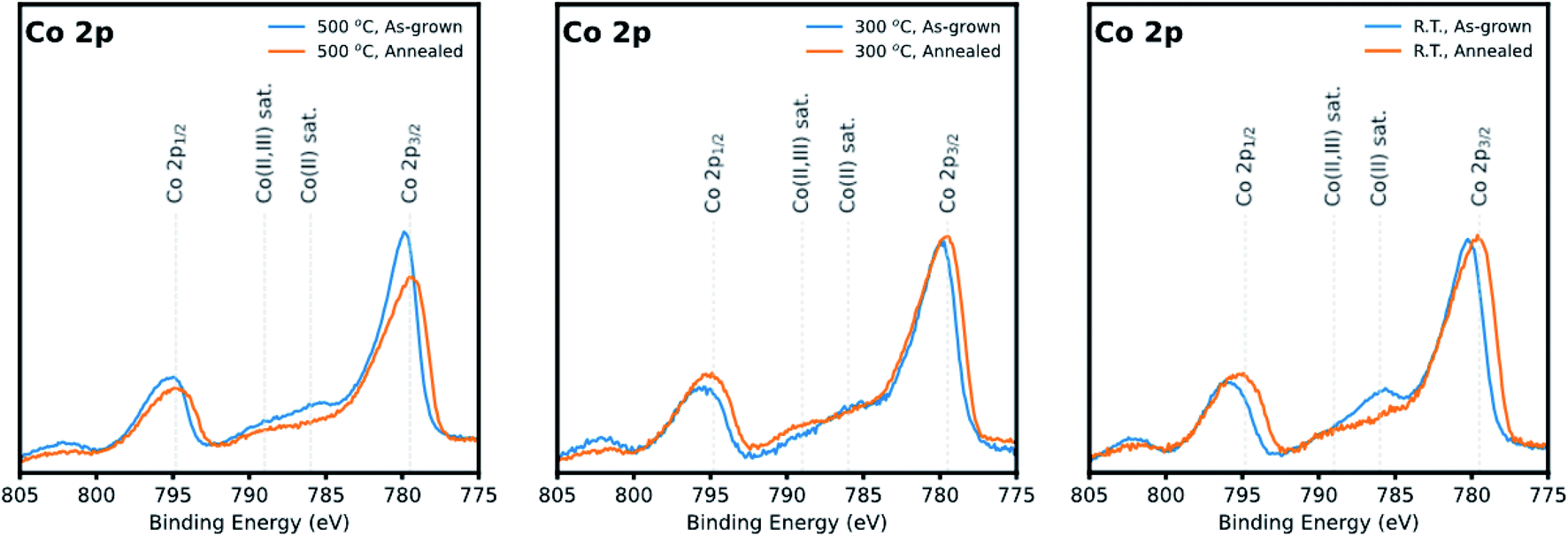 | ||
| Fig. 5 X-ray photoelectron spectra of Co 2p of the LSC nanostructured films grown at 500 °C, 300 °C, and R.T. As-grown films and annealed films are depicted in blue and orange, respectively. | ||
More importantly, the present evidence suggests that even if the initial nanostructure were amorphous or poorly crystalline in the beginning, the as-grown LSC surfaces which initially exhibit metastable structures eventually evolve to a final state with a common chemical environment. Assuming that such surfaces behave similarly upon heating, it is therefore reasonable to assume that in terms of electrode performance, differences in oxygen exchange properties of those surfaces may then be attributed to other external factors such as grain coarsening behaviour, the progression of which may be correlated to any time-dependent degradation of electrochemical performance.
SIMS analysis
SIMS analysis can be considered as a complementary technique to XPS for analyzing the surface composition, although the interpretation of results can be challenging due to possible measurement artefacts that can occur due to matrix effects, ionic mixing, and preferential sputtering.39 It has been noted that preferential sputtering effects may cause some compositional distortion in the immediate sub-surface region (∼1–3 nm) whilst sputter equilibrium is established.40 Here, we employ the SIMS technique to compare the evolution of elemental compositions across different samples from the air/electrode interface to the electrode/electrolyte interface.First, we focus on the SIMS analysis for the regions near the surface. The secondary ion ratios derived from the ToF-SIMS depth profiles of La+, Sr+, and Co+ prepared at 500 °C, 300 °C, and R.T. for both as-grown and annealed samples, are shown in Fig. 6.
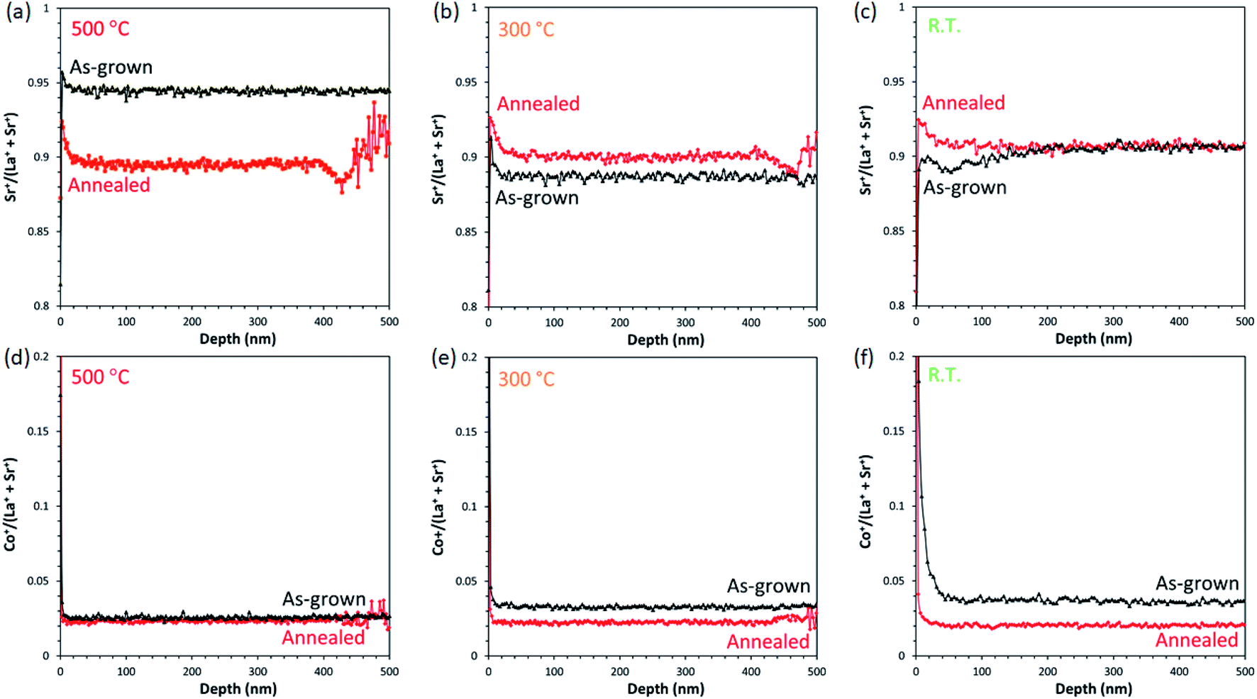 | ||
| Fig. 6 Secondary ion ratios of Sr+/(La+ + Sr+) (top row) and Co+/(La+ + Sr+) (bottom row) derived from ToF-SIMS data for the as-grown and annealed LSC thin films prepared at 500 °C ((a) and (d)), 300 °C ((b) and (e)), and R.T. ((c) and (f)). | ||
We can extract the following observations:
(1) There is no apparent increase of the Sr signal near the surface region for all as-grown samples (Fig. 6(a–c)). In particular, there appears to be an apparent Sr deficiency near the surface of the R.T. sample compared to the samples grown at 300 °C and 500 °C. As there is a relatively high amount of Srsurface which reside on the outermost surfaces of the as-grown R.T. sample (refer to Fig. 3), the lattice-bound Sr deficiency near the surface may be a consequence of Sr out-diffusion behaviour without replenishment from the inner regions of the LSC thin film. This seems reasonable considering that the R.T. film has a highly defective, porous nanostructure where cation diffusion is likely less promoted as compared to a well-crystallized structure. On the other hand, after annealing the samples exhibit an enrichment of Sr near the surface, most especially for the samples deposited at 500 °C and 300 °C. This is consistent with the tendencies reported in literature where Sr enrichment is usually observed near the surface, especially after ageing.15,21,39 It must be noted, though, that the samples in those studies were prepared with different deposition parameters (namely, deposition temperature and oxygen partial pressure) compared to the ones in this study, which would influence the resulting stoichiometric composition as well microstructure of the films.
(2) Another interesting observation is that there appears to be a relative enrichment of Co in the regions close to the surface of the R.T. as-grown sample (Fig. 6(f)). Again, this can be corroborated by the deficiency of lattice-bound Sr, which could account for the higher proportion of Co on the sub-surface. The effect on La is less obvious from these plots, although this will be evident in the depth profiles to be shown later over larger depth scales.
(3) The most important result is that regardless of the initial differences observed for the as-grown samples, long-term annealing at 700 °C reconstructs the surfaces to approximately similar compositions. Sr deficiency disappears almost entirely, and Co enrichment is significantly diminished in comparison to the as-grown sample.
Although the preceding results indicate that the resultant surfaces after annealing tend to be similar for the samples in this study, it is important to note that at relatively high temperatures, cation mobility becomes substantial and diffusion to energetically preferred interfaces can be expected. In a previous study, as revealed by SIMS depth profiling, diffusion couples comprising LSCF thin films on GDC polycrystalline substrates exhibit some diffusion of Sr across LSCF/GDC interfaces after annealing at 800 °C in air.41 To probe the interfaces, we performed SIMS depth profile analyses for all samples up to the LSC/GDC interfaces and the results are shown in Fig. 7.
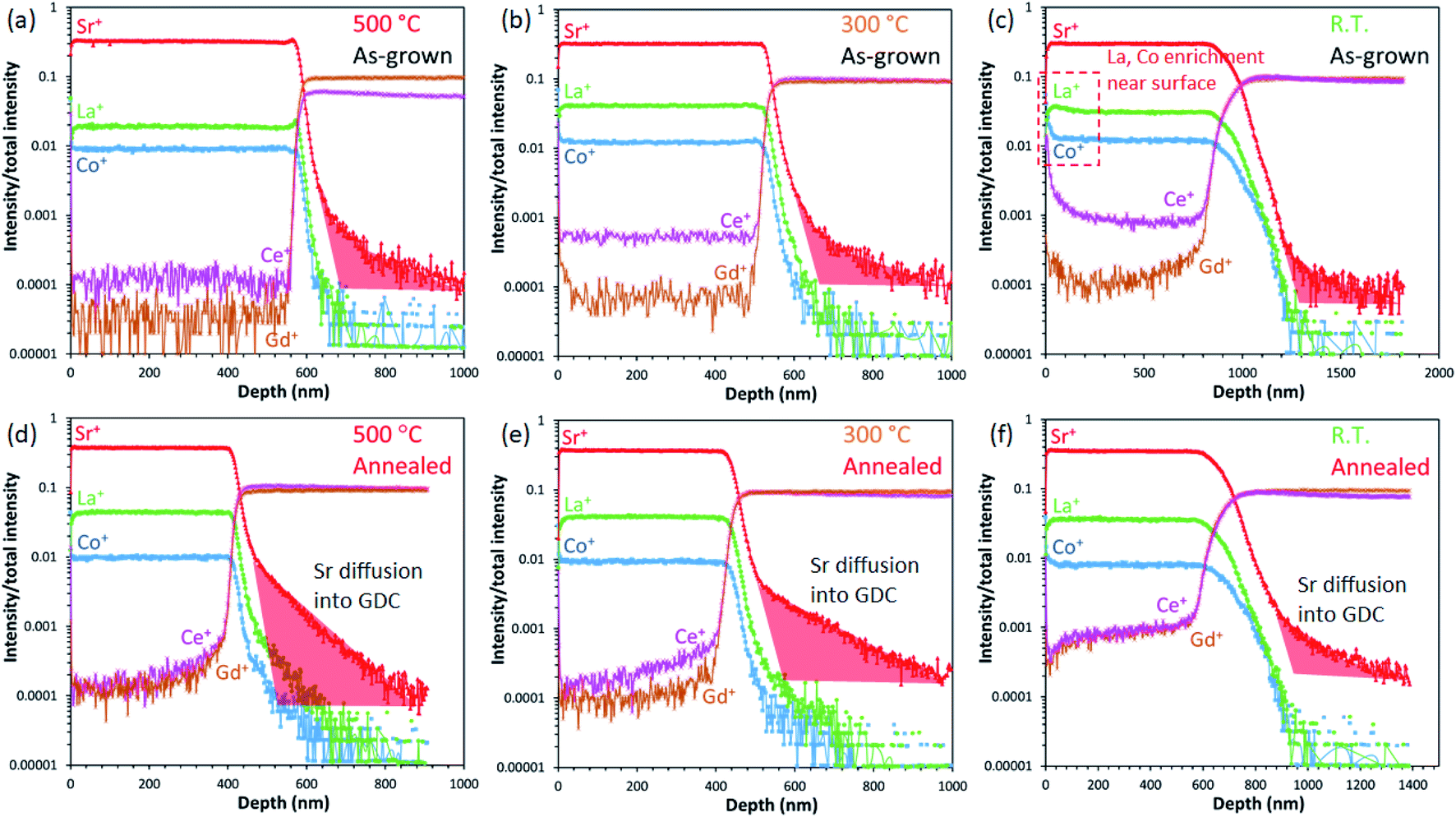 | ||
| Fig. 7 SIMS depth profiles of LSC/GDC samples prepared at (a) 500 °C, (b) 300 °C, and (c) R.T., and annealed samples are shown respectively in (d), (e) and (f). Areas highlighted in red indicate regions of Sr diffusion into the GDC layer. | ||
First, we note that the sharpness of the Ce+ and Gd+ profiles at the LSC/GDC interfaces are likely related to the characteristic porosity of the overlying LSC film and not necessarily indicative of any cation diffusion from the GDC region, i.e., the more porous the film structure is, the broader the profiles appear at the interface due to secondary ions from the inner layers being detected at shallower depths prior to the actual interface. Similarly, the “higher” level of intensities of Ce+ and Gd+ detected in the LSC region may also be accounted for by the existing porosity of the film nanostructure and hence are considered as measurement artefacts. By contrast, the Sr tail into the fully dense GDC region, indicated by the shaded region in red, can be unambiguously correlated to cation diffusion; compared to the as-grown samples, the annealed ones show a more significant broadening of the Sr profiles into GDC. Moreover, the sample prepared at the highest deposition temperature of 500 °C exhibits the broadest diffusion profile among the annealed samples. This suggests that although the surfaces do not seem to show any significant differences in terms of Sr segregation behaviour, the LSC/GDC appears to be an energetically preferred interface where Sr diffusion occurs. Correlating these results to the SEM observations, denser films such as the one prepared at 500 °C likely contain a higher number of cation diffusion paths via grain boundaries which allow the faster diffusion of Sr to the interfaces, whereas films such as the one prepared at R.T. lack such diffusion paths owing to the porous nature of their nanostructures.
Evaluation of electrochemical performance by EIS
For the evaluation of the electrochemical performance, LSC nanostructures were integrated into symmetrical cells as described in Table 1. In order to improve the contact with the GDC substrate, LSCF films were pre-deposited onto GDC substrates prior to the deposition of the LSC thin films. This ensures that the electrode layer is in intimate contact with the GDC substrate and minimizes adhesion issues related to low LSC deposition temperatures.Fig. 8(a–c) show the obtained impedance spectra for the three samples with LSC thin films deposited at various temperatures, showing the data obtained at 700 °C, for t = 0 h and t ∼ 300 h. The spectra show some common features: a noticeable shift of the impedance arcs towards lower ohmic resistance (x-intercept of the high-frequency arc), and an increase in the arc widths which indicate an increase in the electrode polarization resistance. The shift towards lower ohmic resistance may be accounted for by the improvement of contact between the current collecting layer with the thin film electrodes due to the sintering effect.
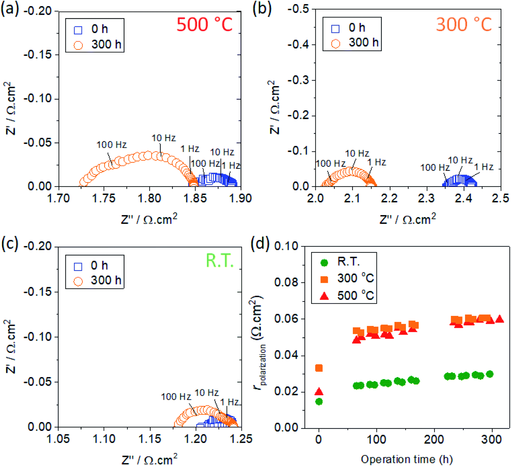 | ||
| Fig. 8 Impedance spectra for LSC thin films deposited at (a) 500 °C, (b) 300 °C, and (c) room temperature (R.T.). The data at t = 0 h and 300 h are depicted by square and circle symbols, respectively. The overall electrode resistance, rpolarization, is plotted versus operation time in (d). 500 °C: red triangles, 300 °C: orange squares, R.T.: green circles. | ||
Furthermore, the total electrode resistance (rpolarization, representing data for a single electrode) is plotted in Fig. 8(d) as a function of time for the three different samples considered in this study. It should be noted that the measured rpolarization possibly includes the contribution of other components in the cell (viz., porous LSC current collector and LSCF thin film), and it would be necessary to separate the contribution of these components to get the sole contribution of the LSC nanostructured electrodes. Nevertheless, considering that all samples are contacted by the same components, we can still extract meaningful comparisons among the samples where the LSC nanostructure is the only variable. The rate of increase of the polarization resistance per unit time (rpolarization/total number of hours) shows a systematic relation with the deposition temperature: the corresponding values are 0.13, 0.09, and 0.05 mΩ cm2 h−1 for 500 °C, 300 °C, and R.T., respectively. Interestingly, we find that the rpolarization values are quite comparable among the samples at t = 0, but the values diverge at t > 0 resulting to an almost three-fold increase observed for the samples deposited at 300 °C and 500 °C. By comparison, the R.T. sample exhibited a relatively slower degradation, leading to a final rpolarization value (at t = 300 h) of only ∼0.03 Ω cm2. To our knowledge, this is the first long-term evaluation of LSC nanostructured thin films demonstrating very low electrode resistance even after ∼300 h of testing. On the other hand, the initial rapid increase observed in the first ∼50 h appears to be analogous for all samples, and can be correlated to the drastic microstructural changes (Fig. 1 and 2) due to granular sintering induced with prolonged heating at 700 °C.
To analyze the impedance spectra, we adopt the distribution of relaxation times (DRT) analysis to deconvolute the various electrode reactions. Here, we could identify three characteristics peaks occurring at high (40–250 Hz), medium (5–40 Hz), and low frequency (0.3–5 Hz) range. This is illustrated by the DRT spectra shown in Fig. 9(a). Analogous to the DRT results reported for LSC multilayer films in a previous study,23 we can tentatively assign Peak 1 to the interfacial resistance (electrode–electrolyte resistance), Peak 2 to the surface adsorption/dissociation of oxygen into active O-species, and Peak 3 to the gas conversion resistance. Here, the largest contribution is attributed to Peak 2, which suggests that the degradation in performance is determined largely by the oxygen exchange properties of the electrodes. Considering that the surface conditions of the LSC thin films share common features, the differences in oxygen exchange properties can thus be accounted for by the microstructural features such as surface area and film porosity, which vary greatly among the samples. It can also be observed that the Peak 2 contribution shows a gradually increasing trend with time for all samples, suggesting a degradation behaviour consistent with time-dependent grain coarsening effects.18 Similarly, a gradual degradation with time can be observed for the electrode–electrolyte resistance (Peak 1), albeit to a smaller extent. On the other hand, the contribution associated to the gas conversion (Peak 3) only shows a drastic increase in the beginning but appear to reach saturation levels for all samples. This behaviour can be reasonably explained by microstructural changes in the electrode which physically influence the gas diffusion. For all components the R.T. sample outperforms those deposited at higher temperatures, exhibiting the lowest rpolarization values for the entire range of time investigated. To further explain the relatively low electrode resistance for the R.T. sample, post-mortem characterizations of selected samples after testing will be presented in the next section.
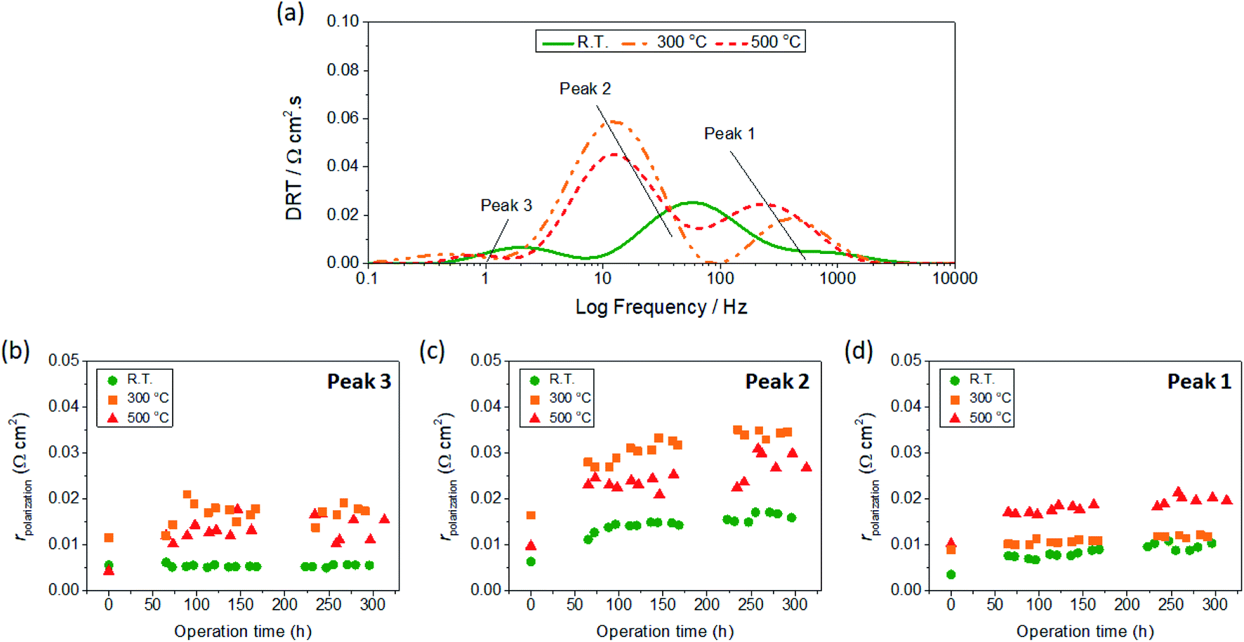 | ||
| Fig. 9 (a) DRT spectra obtained for the symmetrical cells with LSC thin films deposited at 500 °C, 300 °C, and R.T. after testing at 700 °C and t ∼ 300 h. Three characteristic peaks corresponding to different physical processes related to reactions occurring at the electrodes are identified as Peak 3, Peak 2, and Peak 1. The plots of rpolarization values corresponding to the different peaks are shown in (b–d). 500 °C: red triangles, 300 °C: orange squares, R.T.: green circles. | ||
Post-mortem characterization
To examine the post-mortem structures of the symmetrical cells after long-term testing, detailed characterizations were performed using SEM and S/TEM analyses. The representative SEM images of the surfaces and cross-sections of the cells are shown in the ESI, Fig. S2.† Consistent with the observations for the bare LSC surfaces in the preceding section, the LSC nanostructures are characterized by different morphologies depending on the deposition temperature, with the R.T. sample showing much higher porosities which were retained even after prolonged exposure to high temperature.Details of the nanostructures are further revealed in the TEM images shown in Fig. 10, where the cross-sections of the LSC samples prepared at 500 °C and R.T. are compared. As depicted in Fig. 10(a), the LSC film prepared at 500 °C exhibits a semi-homogeneous structure containing several closed pores. A dark contrast can be further observed at the LSC region adjacent to the LSC/LSCF interface, which may indicate the presence of strain and/or defects formed in this region. On the other side of the LSCF layer, the GDC region adjacent to the LSCF/GDC interface similarly exhibits a dark contrast, which additionally suggests some interaction also occurred between the LSCF and GDC layers. By contrast, the LSC film prepared at R.T. shown in Fig. 10(b) exhibits a highly porous structure comprising nanoclusters. The nanoclusters themselves are comprised of several nanograins ranging in 50 to 100 nm in size and stacked on top of each other. Based on the evaluation of performance presented in the previous section, it seems that the retention of a high surface exchange property can be correlated to this unique nanostructure, which presents a high porosity to aid gas diffusion as well as a high surface area for the ORR. Moreover, the LSC/LSCF and LSCF/GDC interfaces appear sharp and well-defined, and the regions adjacent to the corresponding interfaces do not exhibit any particular defects.
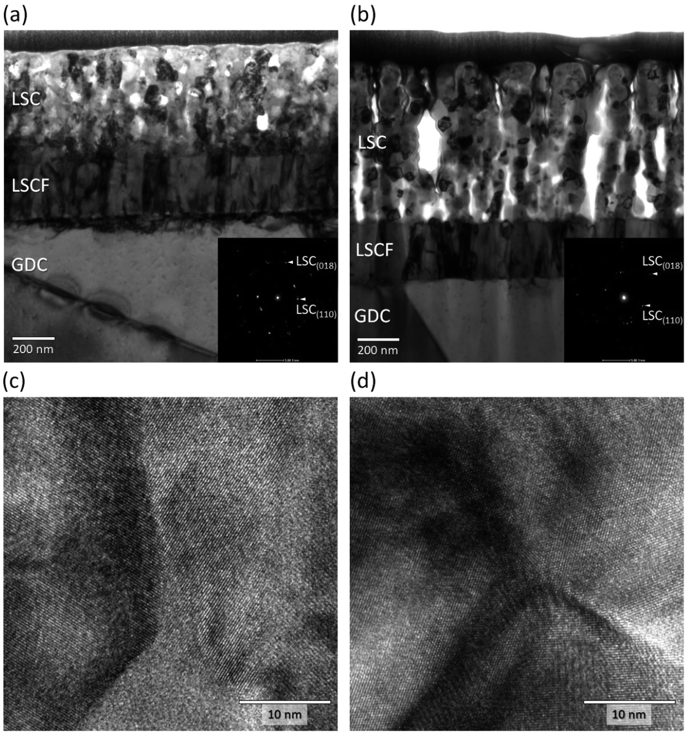 | ||
| Fig. 10 Representative TEM micrographs of LSC/LSCF/GDC symmetrical cells after long-term testing at 700 °C for 300 h in air. (a) LSC film prepared at 500 °C, (b) LSC film prepared at R.T. Insets are corresponding selected area electron diffraction patterns obtained in the respective LSC regions. High-magnification TEM micrographs showing lattice images taken near the surface of the (c) LSC film prepared at 500 °C, and (d) LSC film prepared at R.T. | ||
The insets in Fig. 10(a) and (b) show the selected area electron diffraction patterns obtained for the LSC layers; the diffraction spots can be indexed to the LSC rhombohedral structure. Furthermore, typical high-magnification TEM images measured near the surface of the LSC regions are shown in Fig. 10(c) and (d). The highly ordered lattice images obtained for both samples confirm the highly crystalline nature of the LSC layers; in other words, even if the films were initially amorphous or poorly crystalline due to the low-temperature deposition employed, their subsequent prolonged exposure to sufficiently high temperatures in air promotes crystallinity and thereby changes the film properties to a common final state. The present data do not indicate that a less crystalline state for the LSC thin film is more beneficial in terms of driving the ORR activity due to any suppression of Sr segregation; in fact, XPS results shown earlier revealed that the R.T.-deposited film appears to have more Sr-rich phases on its outermost surface compared to those prepared at higher temperatures. These results lead us to believe that the main advantage for low-temperature deposition is the incorporation of nanoscaled porosities which not only result to a much higher surface area but also significantly reduced intergrain contact, and consequently suppression of degradation due to grain coarsening.
As the LSC thin films were contacted by thick current collecting layers for the impedance measurements, it would be difficult to probe the surfaces of the samples using XPS, or analyze the interfaces using depth profiling by SIMS. To obtain accurate information about the film compositions, STEM-EDX analysis was performed for the samples and the elemental mapping results are presented in Fig. 11. As shown in Fig. 11(a), the elemental distribution across the cross-section of the 500 °C sample does not indicate any specific inhomogeneities within the films or the interfaces, although the mapping for Fe clearly shows some diffusion from the LSCF into the LSC layer. The effect of Fe diffusion into LSC is not yet clear at this point, though a depletion of Fe from the LSCF region at the LSC/LSCF interface could presumably lead to changes in its stoichiometric composition in the vicinity. Furthermore, the STEM-HAADF image reveals the formation of voids (denoted by black arrows) along the LSCF/GDC interface, similarly indicating some enhanced diffusion processes between these two layers.42 In contrast, the R.T. sample shown in Fig. 11(b) shows well-defined interfaces; in particular the lack of void formation along the LSCF/GDC is in stark contrast to that of the 500 °C sample, which suggests that the stability of the LSCF/GDC interface is somehow affected by the type of LSC nanostructure even though it is located away from this region. The respective STEM-EDX profiles generated from the elemental maps (integrated over the thickness of the specimen) are shown in Fig. 11(a) and (b), with the corresponding elemental profiles depicted in atomic percent (top plot) and the Sr/(La + Sr) ratio derived from the Sr and La profiles (bottom plot). A noticeable difference is that the relative concentration of Sr shows an increasing tendency towards the LSCF/GDC region for the 500 °C sample whereas the R.T. sample shows a fairly constant Sr profile throughout the LSC and LSCF regions. This is consistent with the SIMS results shown earlier which indicated Sr diffusion to the LSC/GDC interface. These results further confirm that whereas no obvious Sr segregation towards the film surfaces is evident, the interior regions of the film show active Sr diffusion from the electrode towards the interface with the GDC electrolyte. For the case of the 500 °C sample, the void formation can therefore be associated to the Sr diffusion across the LSCF/GDC interface. These results could also reasonably explain the observed degradation of the interfacial resistance associated to the electrode/electrolyte interface (Peak 3 in the DRT analysis) for this sample. Furthermore, these results highlight the interplay between surfaces and interfaces in describing the electrode degradation behaviour.
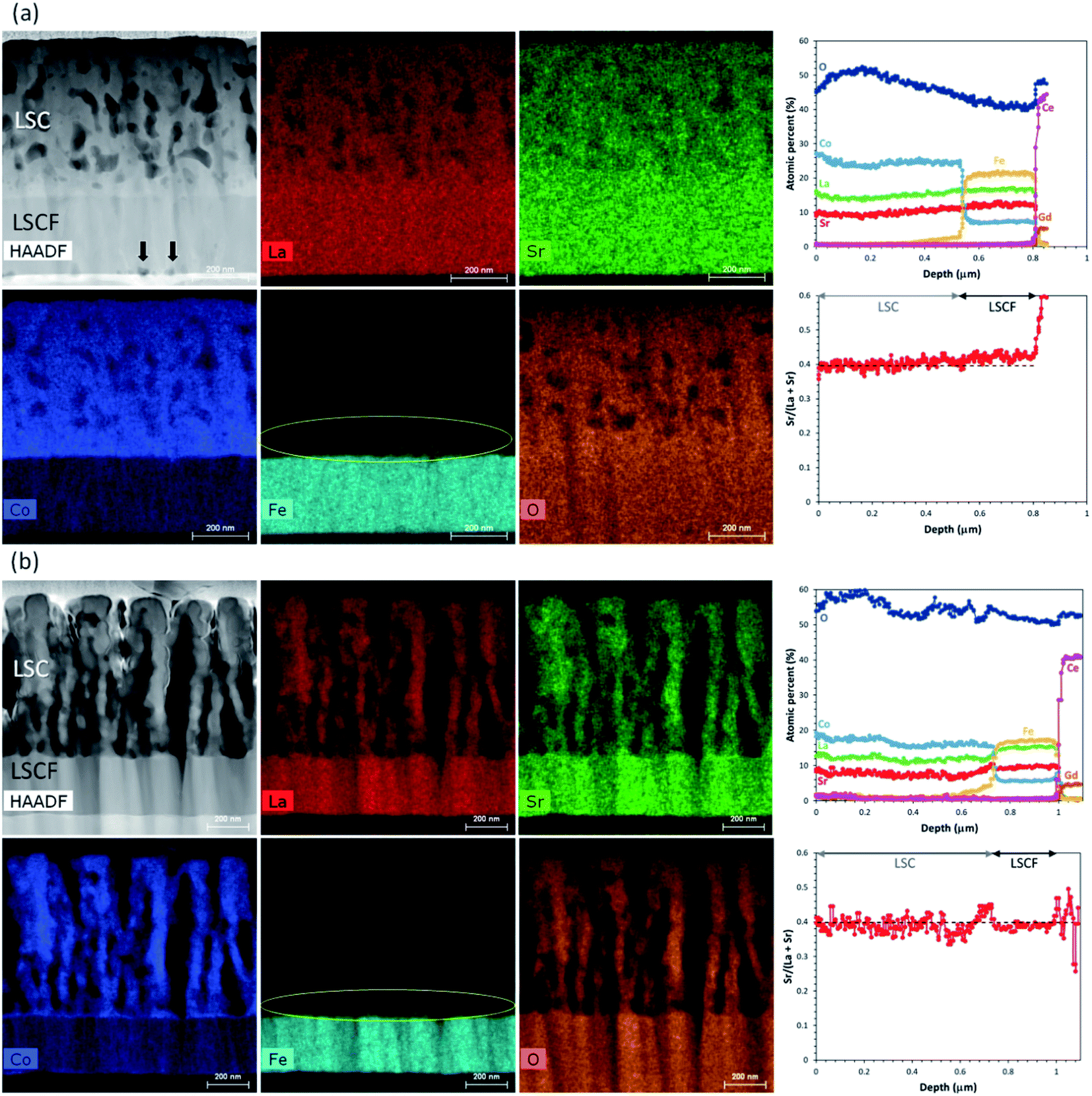 | ||
| Fig. 11 STEM-EDX elemental mapping for the cells utilizing (a) LSC film prepared at 500 °C, (b) LSC film prepared at R.T. Black arrows in (a) denote voids that appeared at the LSCF/GDC interface. On the Fe mapping results shown in (a) and (b), yellow oval circles highlight regions where Fe diffusion from LSCF into LSC is observed. The respective plots on the right column are STEM-EDX profiles generated from the elemental maps, showing the various elemental components in atomic percent (top plot), and the relative concentration of Sr, expressed as Sr/(La + Sr) (bottom plot). | ||
Conclusions
In this study, we examined the effect of processing temperatures, namely film deposition and annealing, on the performance and stability of LSC thin film nanostructures. The characteristic nanostructures of LSC thin films were tuned by varying the deposition temperature from relatively low temperatures of 500 °C down to room temperature. From detailed characterizations including XPS, SIMS, and S/TEM, it is found that the as-grown LSC surfaces initially exhibit metastable structures with a characteristically high concentration of Srsurface and a high proportion Co2+ especially for room-temperature deposited samples. However, upon subsequent annealing at 700 °C in air, the LSC surfaces undergo a drastic reconstruction resulting in more energetically stable surfaces with mostly lattice-bound Sr and containing Co3+. Analysis of the regions close to the films' surfaces did not show any remarkable Sr segregation before annealing, though comparable levels of Sr enrichment near the surfaces of the samples were confirmed after annealing at 700 °C for 300 h in air. On the other hand, analysis of the LSC/GDC interfaces shows that the extent of Sr diffusion into the GDC region is dependent on the deposition temperature, indicating that even though there does not appear to be significant tendencies for Sr segregation to the films' surfaces, cation diffusion behaviour across the electrode–electrolyte interfaces is influenced by the processing temperature.Based on symmetrical cells tested at 700 °C for 300 hours, the cells utilizing LSC thin films deposited at room temperature exhibited the best electrochemical performance in terms of relatively lower values of the electrode polarization resistance and lower degradation rate compared to those prepared under higher deposition temperatures. Analysis of the impedance spectra using DRT method showed that the time-dependent performance degradation arises mainly from degradation of oxygen surface exchange properties, which is accounted for by the granular sintering and coarsening behaviour at high temperatures, and degradation of interfacial properties, which is governed by the thermally activated cation diffusion behaviour. This work highlights the dynamic interrelation between surfaces and interfaces as influenced by processing temperatures and their impact on the electrochemical performance of nanostructured thin film electrodes.
Author contributions
Katherine Develos-Bagarinao: conceptualization, formal analysis, investigation, writing-original draft. Ozden Celikbilek: investigation, formal analysis, writing – review & editing. Riyan A. Budiman: investigation, visualization, formal analysis, writing – review & editing. Gwilherm Kerherve: investigation, visualization, formal analysis, writing – review & editing. Sarah Fearn: investigation, formal analysis, writing – review & editing. Stephen J. Skinner: formal analysis, writing – review & editing. Haruo Kishimoto: conceptualization, formal analysis, supervision, writing – review & editing.Conflicts of interest
There are no conflicts to declare.Acknowledgements
The authors are grateful for the assistance of M. Sugasawa in the PLD experiments and EIS measurements, and N. Saitou (TIA-EM) for assistance in the S/TEM characterizations. The authors thank K. Yamaji and T. Ishiyama (iECO, AIST) for fruitful discussions. O. Celikbilek has received funding from the European Union's Horizon 2020 Research and Innovation Programme under the Marie Sklodowska-Curie grant agreement no. 836503.Notes and references
- N. Tsvetkov, Q. Lu, L. Sun, E. J. Crumlin and B. Yildiz, Nat. Mater., 2016, 15, 1010–1016 CrossRef CAS PubMed.
- M. Trini, A. Hauch, S. De Angelis, X. Tong, P. V. Hendriksen and M. Chen, J. Power Sources, 2020, 450, 227599 CrossRef CAS.
- H. S. Noh, H. Lee, B. K. Kim, H. W. Lee, J. H. Lee and J. W. Son, J. Power Sources, 2011, 196, 7169–7174 CrossRef CAS.
- A. V. Berenov, A. Atkinson, J. A. Kilner, E. Bucher and W. Sitte, Solid State Ionics, 2010, 181, 819–826 CrossRef CAS.
- J. Januschewsky, M. Ahrens, A. Opitz, F. Kubel and J. Fleig, Adv. Funct. Mater., 2009, 19, 3151–3156 CrossRef CAS.
- D. Lee, R. Jacobs, Y. Jee, A. Seo, C. Sohn, A. V. Ievlev, O. S. Ovchinnikova, K. Huang, D. Morgan and H. N. Lee, J. Phys. Chem. C, 2017, 121, 25651–25658 CrossRef CAS.
- D. Udomsilp, J. Rechberger, R. Neubauer, C. Bischof, F. Thaler, W. Schafbauer, N. H. Menzler, L. G. J. de Haart, A. Nenning, A. K. Opitz, O. Guillon and M. Bram, Cell Rep. Phys. Sci., 2020, 1, 100072 CrossRef.
- F. Han, R. Mücke, T. Van Gestel, A. Leonide, N. H. Menzler, H. P. Buchkremer and D. Stöver, J. Power Sources, 2012, 218, 157–162 CrossRef CAS.
- D.-H. Myung, J. Hwang, J. Hong, H.-W. Lee, B.-K. Kim, J.-H. Lee and J.-W. Son, J. Electrochem. Soc., 2011, 158, B1000–B1006 CrossRef CAS.
- A. Egger, M. Perz, E. Bucher, C. Gspan and W. Sitte, Fuel Cells, 2019, 19, 458–471 CAS.
- K. Develos-Bagarinao, J. De Vero, H. Kishimoto, T. Ishiyama, K. Yamaji, T. Horita and H. Yokokawa, Phys. Chem. Chem. Phys., 2019, 21, 7183–7195 RSC.
- R. A. Budiman, S. S. Liu, K. D. Bagarinao, T. Ishiyama, H. Kishimoto, K. Yamaji, T. Horita and H. Yokokawa, J. Electrochem. Soc., 2019, 166, F414–F422 CrossRef CAS.
- R. A. Budiman, K. D. Bagarinao, S. S. Liu, D. H. Cho, T. Ishiyama, H. Kishimoto, K. Yamaji, T. Horita and H. Yokokawa, J. Electrochem. Soc., 2018, 165, F1206–F1216 CrossRef CAS.
- M. Siebenhofer, T. M. Huber, G. Friedbacher, W. Artner, J. Fleig and M. Kubicek, J. Mater. Chem. A, 2020, 8, 7968–7979 RSC.
- O. Celikbilek, A. Cavallaro, G. Kerherve, S. Fearn, O. Chaix-Pluchery, A. Aguadero, J. A. Kilner and S. J. Skinner, ACS Appl. Mater. Interfaces, 2020, 12, 34388–34401 CrossRef CAS.
- J. Hayd, H. Yokokawa and E. Ivers-Tiffee, J. Electrochem. Soc., 2013, 160, F351–F359 CrossRef CAS.
- J. Hayd, L. Dieterle, U. Guntow, D. Gerthsen and E. Ivers-Tiffée, J. Power Sources, 2011, 196, 7263–7270 CrossRef CAS.
- M. Shah, P. W. Voorhees and S. A. Barnett, Solid State Ionics, 2011, 187, 64–67 CrossRef CAS.
- I. A. Ovid’ko and A. G. Sheinerman, Philos. Mag., 2003, 83, 1551–1563 CrossRef.
- M. Kubicek, G. M. Rupp, S. Huber, A. Penn, A. K. Opitz, J. Bernardi, M. Stöger-Pollach, H. Hutter and J. Fleig, Phys. Chem. Chem. Phys., 2014, 16, 2715–2726 RSC.
- Z. Cai, M. Kubicek, J. Fleig and B. Yildiz, Chem. Mater., 2012, 24, 1116–1127 CrossRef CAS.
- A. Cavallaro, S. S. Pramana, E. Ruiz-Trejo, P. C. Sherrell, E. Ware, J. A. Kilner and S. J. Skinner, Sustainable Energy Fuels, 2018, 2, 862–875 RSC.
- K. Develos-Bagarinao, R. A. Budiman, T. Ishiyama, K. Yamaji and H. Kishimoto, J. Power Sources, 2020, 480, 229094 CrossRef CAS.
- A. Infortuna, A. S. Harvey and L. J. Gauckler, Adv. Funct. Mater., 2008, 18, 127–135 CrossRef CAS.
- P. Plonczak, A. Bieberle-Huetter, M. Sogaard, T. Ryll, J. Martynczuk, P. V. Hendriksen and L. J. Gauckler, Adv. Funct. Mater., 2011, 21, 2764–2775 CrossRef CAS.
- K. Develos-Bagarinao, H. Kishimoto, K. Yamaji, T. Horita and H. Yokokawa, Nanotechnology, 2015, 26, 215401 CrossRef.
- K. Develos-Bagarinao, J. De Vero, H. Kishimoto, T. Ishiyama, K. Yamaji, T. Horita and H. Yokokawa, Nano Energy, 2018, 52, 369–380 CrossRef CAS.
- N. H. Perry, G. F. Harrington and H. L. Tuller, in Metal Oxide-Based Thin Film Structures: Formation, Characterization and Application of Interface-Based Phenomena, ed. N. Pryds and V. Esposito, Elsevier Inc., 2018 Search PubMed.
- G. M. Rupp, H. Téllez, J. Druce, A. Limbeck, T. Ishihara, J. Kilner and J. Fleig, J. Mater. Chem. A, 2015, 3, 22759–22769 RSC.
- J. Druce, H. Téllez and J. Hyodo, MRS Bull., 2014, 39, 810–815 CrossRef CAS.
- M. Niania, R. Podor, T. Ben Britton, C. Li, S. J. Cooper, N. Svetkov, S. Skinner and J. Kilner, J. Mater. Chem. A, 2018, 6, 14120–14135 RSC.
- B. Koo, K. Kim, J. K. Kim, H. Kwon, J. W. Han and W. C. Jung, Joule, 2018, 2, 1476–1499 CrossRef CAS.
- L. Zhao, J. Drennan, C. Kong, S. Amarasinghe and S. P. Jiang, J. Mater. Chem. A, 2014, 2, 11114–11123 RSC.
- Y. Tsuji, S. Sako, K. Nitta, K. Yamamoto, Y. Shao-Horn, Y. Uchimoto and Y. Orikasa, Solid State Ionics, 2020, 357, 115502 CrossRef CAS.
- F. Piskin, R. Bliem and B. Yildiz, J. Mater. Chem. A, 2018, 6, 14136–14145 RSC.
- Y. Yu, K. F. Ludwig, J. C. Woicik, S. Gopalan, U. B. Pal, T. C. Kaspar and S. N. Basu, ACS Appl. Mater. Interfaces, 2016, 8, 26704–26711 CrossRef CAS.
- C. A. F. Vaz, D. Prabhakaran, E. I. Altman and V. E. Henrich, Phys. Rev. B: Condens. Matter Mater. Phys., 2009, 80, 155457 CrossRef.
- J. G. Kim, D. L. Pugmire, D. Battaglia and M. A. Langell, Appl. Surf. Sci., 2000, 165, 70–84 CrossRef CAS.
- M. Kubicek, A. Limbeck, T. Frömling, H. Hutter and J. Fleig, J. Electrochem. Soc., 2011, 158, B727–B734 CrossRef CAS.
- M. Niania, M. Sharpe, R. Webb and J. A. Kilner, Nucl. Instrum. Methods Phys. Res., Sect. B, 2020, 480, 27–32 CrossRef CAS.
- J. C. De Vero, H. Yokokawa, K. Develos-Bagarinao, S.-S. Liu, H. Kishimoto, T. Ishiyama, K. Yamaji and T. Horita, MRS Commun., 2019, 9, 236–244 CrossRef CAS.
- F. Tietz, D. Sebold, A. Brisse and J. Schefold, J. Power Sources, 2013, 223, 129–135 CrossRef CAS.
Footnotes |
| † Electronic supplementary information (ESI) available. See DOI: 10.1039/d1ta07235h |
| ‡ Present address: Université Grenoble Alpes, CNRS, Grenoble INP, LMGP, Grenoble 38000, France. |
| § Thermo Fisher Scientific. Avantage Software. https://xpssimplified.com/avantage_data_system.ph, 2019. |
| This journal is © The Royal Society of Chemistry 2022 |