
Multi-scale chemo-mechanical evolution during crystallization of mixed conducting SrTi0.65Fe0.35O3−δ films and correlation to electrical conductivity
Haley B.
Buckner
ab,
Qing
Ma
 c,
Joshua
Simpson-Gomez
ab,
Emily J.
Skiba
ab and
Nicola H.
Perry
*ab
c,
Joshua
Simpson-Gomez
ab,
Emily J.
Skiba
ab and
Nicola H.
Perry
*ab
aDepartment of Materials Science & Engineering, University of Illinois at Urbana-Champaign, 1304 W. Green St., Urbana, IL 61801, USA. E-mail: nhperry@illinois.edu
bMaterials Research Laboratory, University of Illinois at Urbana-Champaign, 104 S. Goodwin Ave, Urbana, IL 61801, USA
cDND-CAT, Northwestern Synchrotron Research Center at the Advanced Photon Source Argonne, IL 60439, USA
First published on 20th October 2021
Abstract
Recent work has demonstrated a low-temperature route to fabricating mixed ionic/electronic conducting (MIEC) thin films with enhanced oxygen exchange kinetics by crystallizing amorphous-grown thin films under mild temperatures, eluding conditions for deleterious A-site cation surface segregation. Yet, the complex, multiscale chemical and structural changes during MIEC crystallization and their implications for the electrical properties remain relatively unexplored. In this work, micro-structural and atomic-scale structural and chemical changes in crystallizing SrTi0.65Fe0.35O3−δ thin films on insulating (0001)-oriented Al2O3 substrates are observed and correlated to changes in the in-plane electrical conductivity, measured in situ by ac impedance spectroscopy. Synchrotron X-ray absorption spectroscopy at the Fe and Ti K-edges gives direct evidence of oxidation occurring with the onset of crystallization and insight into the atomic-scale structural changes driven by the chemical changes. The observed oxidation, increase in B-site polyhedra symmetry, and alignment of neighboring B-site cation coordination units demonstrate increases in both hole concentration and mobility, thus underpinning the measured increase of in-plane conductivity by over two orders of magnitude during crystallization. High resolution transmission electron microscopy and spectroscopy of films at various degrees of crystallinity reveal compositional uniformity with extensive nano-porosity in the crystallized films, consistent with solid phase contraction expected from both oxidation and crystallization. We suggest that this chemo-mechanically driven dynamic nano-structuring is an additional contributor to the observed electrical behavior. By the point that the films become ∼60% crystalline (according to X-ray diffraction), the conductivity reaches the value of dense, fully crystalline films. Given the resulting high electronic conductivity, this low-temperature processing route leading to semi-crystalline hierarchical films exhibits promise for developing high performance MIECs for low-to-intermediate temperature applications.
1. Introduction
Non-crystalline materials have demonstrated distinct advantages in processability, stability, and tunability1–3 for use in a wide range of applications like high-k dielectrics,4,5 resistive switching devices,6,7 and all-solid-state battery electrolytes.3,8–12 Yet, the effects of amorphization and crystallization have only been studied in a few mixed ionic and electronic conductors (MIECs). One such composition, SrTi0.65Fe0.35O3−δ (STF35), is an ideal model mixed conductor for the study of amorphous-to-crystalline behavior and is of practical interest in its crystalline form for high temperature applications, such as gas sensors, gas separation membranes, and electrodes for fuel and electrolysis cells. In these high-temperature conditions, the oxygen content13 and corresponding electrical behavior14 have been well characterized in bulk ceramics. Under mildly oxidizing conditions, as used in the present work, an increase in oxygen content is balanced by an increase in hole concentration to satisfy the electroneutrality condition.The potential benefits of harnessing the amorphous-to-crystalline transition are two-fold. First, it offers a low-thermal-budget processing route. While traditional, high temperature processing of MIEC perovskites has been shown to lead to significant surface segregation of Sr or other large A-site cations,15–17 we showed in previous work that low temperature processing suppresses the Sr segregation and mitigates its detrimental effects on the surface oxygen exchange kinetics.18 The low-temperature processing is also intrinsically less energy intensive and allows for the use of more thermally sensitive or flexible substrates. More fundamentally, the crystallization behavior of this class of materials has not been as well explored as in some other classes, underlining the importance of understanding how and why crystallinity impacts the properties of MIEC materials. Exploring this low-temperature behavior may extend application of STF35 and other MIECs to wider classes of devices or open up new device possibilities. For example, STF was recently explored as an oxygen evolution catalyst in alkaline media.19
The impact of crystallinity on the oxygen surface exchange kinetics of MIECs has been explored in La0.6Sr0.4CoO3−δ (LSC),20–22 SrTi0.65Co0.35O3−δ (STC35),23 Sr2Ti0.65Fe0.35O4±δ (RP-STF35),23 and SrTi0.65Fe0.35O3−δ (STF35).18,23,24 For all four compositions, the degree of crystallinity was reduced by lowering the deposition temperature and resulted in enhanced surface exchange coefficients, kchem or k*, in the poorly crystalline vs. fully crystalline films. X-ray amorphous LSC was grown at temperatures below 470 °C,20–22 and nano-porosity in as-deposited films could be introduced through high oxygen partial pressures22 during deposition. Though operation at higher temperatures likely resulted in nanocrystalline (rather than amorphous) LSC films, an increased oxygen diffusion coefficient,21D*, and improved (lower) polarization resistance20 when operating as a fuel cell cathode were also observed. With a semi-crystalline and nano-porous LSC cathode in a micro solid oxide fuel cell, power densities as high as 260 mW cm−2 at temperatures as low as 425 °C were achieved.22 For STF35, RP-STF35, and STC35, room-temperature deposition (amorphous) followed by brief mild-temperature annealing (just crystallized) led to kchem values much higher than traditional high-temperature fully crystalline-grown films, whereas amorphous films did not exhibit measurable oxygen exchange ability. Two notable structural/chemical features accompanied the high kchem values: (1) STF35, STC35, and RP-STF35 semi-crystalline films contained nano-scale open porosity, a microstructure significantly differing from the dense, columnar grains observed in crystalline-grown thin films on the same lattice-mismatched substrates.18,23 (2) The amorphous-grown STF35, STC35, and RP-STF35 thin films were also suspected to be more reduced than their crystalline-grown counterparts based on their color, with semi-crystalline films somewhat intermediate. For STF35 it has been shown directly that optical absorption changes at key wavelengths are linearly proportional to oxygen and hole concentrations, and that transmitted light intensity through the films decreased dramatically at the crystallization point.25 While these observations lend more evidence supporting the promise of semi-crystalline MIECs in low-to-intermediate temperature applications, a number of open questions remain. Specifically, the reasons for the enhanced k values and development of the hierarchical nanostructures have not been fully explored. We hypothesized that oxidation accompanies crystallization in these MIECs, which would have important implications for (a) formation of the hierarchical microstructure, where contractive strain arising from both crystallization and oxidation would drive its evolution, and (b) evolving point defect chemistry and associated functional properties (surface exchange coefficient, oxygen diffusivity, electronic conductivity).
Therefore, in this work, both micro-structural and atomic-scale structural and chemical changes in crystallizing STF35 thin films on insulating (0001)-oriented Al2O3 substrates were observed and correlated to changes in the in-plane electrical conductivity, measured in situ by ac impedance spectroscopy. Based on sequential synchrotron X-ray absorption spectroscopy of the Fe K-edge, we find evidence for oxidation during crystallization, accompanied by increases in symmetry of individual B-site cation coordination units and alignment of neighboring B-site polyhedra. These local changes indicate both increasing hole concentration and hole mobility during crystallization, and they help to explain the orders-of-magnitude increase in isothermal conductivity. High resolution transmission electron microscopy at various stages of crystallization demonstrates appearance of nanoscale crystallites and pores, where the high pore volume fraction is consistent with solid-phase contraction attributed to both crystallization and oxidation. We suggest that this chemo-mechanically driven nano-structural evolution is an additional contributor to the observed electrical behavior. By the point that the films become ∼60% crystalline (according to X-ray diffraction), the conductivity reaches the value of dense, fully crystalline films. High resolution spectroscopy suggests the films retain compositional uniformity with no evidence for Sr segregation at pore surfaces. These results further suggest promise for use of semi-crystalline mixed conductors and provide some insight into the previous observations of dramatic increases in surface exchange coefficients during crystallization.
2. Experimental methods
2.1 Thin film fabrication
Amorphous SrTi0.65Fe0.35O3−δ (STF35) thin films, 200 nm thick, were deposited on single crystalline Al2O3 substrates (MTI Corp, (0001) orientation) via room-temperature pulsed laser deposition (PLD) using a 248 nm KrF excimer laser (Lambda Physick, LPX 210) operating at 5 Hz. The energy of the laser was ∼350 mJ, measured outside the chamber, and the oxygen pressure was set to 35 mTorr. The growth rate was calibrated using X-ray reflectivity. While the films were each grown separately, the depositions were performed close together in time to ensure consistent initial amorphous structures. The PLD target was prepared via solid state synthesis, using conditions described previously.262.2 Structural characterization
For structural characterization, amorphous STF35 thin films were inserted individually into a pre-heated furnace for rapid heating with a controlled gas atmosphere (∼0.2 atm O2, 0.8 atm Ar) using high purity gases and a 100 sccm rotameter-controlled flow rate. Each sample was annealed once for a time in the range of 0 min to 48 h during a 400 °C isothermal hold and quenched. The degree of crystallinity of each annealed film was evaluated using X-ray diffraction (Bruker, D8 Advance) with Bragg–Brentano geometry and Cu Kα radiation. Each measurement, including a blank substrate, was aligned to the sapphire (0001) peak, and the profiles were fit with a Pseudo-Voigt function with split peak shape and width asymmetry corrections in the Highscore Plus software (Malvern Panalytical) to obtain an overall profile fit and background intensity fit. To account for variations in initial X-ray intensity between measurements, each XRD pattern was scaled to align the background intensity at the sapphire peak position (∼41.7° 2θ) to that of the blank substrate. The substrate contribution was then subtracted to isolate the signal from the annealed films. The total area and background area were calculated using a left Riemann sum from the fit profiles, and the volume fraction crystalline was calculated by dividing the peak area by the total area. This degree of crystallinity (DOC) method does not require any external/internal standards or calibration samples and is described in full in Riello27 and references therein.A ∼10 nm surface of Au/Pd (Emitech) was deposited onto the surface of the annealed films (5 min, 20 min, 23 h) to prevent charge build up, and cross sections were prepared for (scanning) transmission electron microscopy (S/TEM) and energy dispersive X-ray spectroscopy (EDS) using a lift-out technique with a dual-beam focused ion beam/scanning electron microscope (Scios2 SEM/FIB, Thermo) after depositing an additional ∼2 μm Pt surface protection layer. The cross sections were prepared and thinned at 30 kV, and further thinning was carried out at 5 kV and then 2 kV to reduce beam damage to the lamellae. The microstructure and crystallinity were analyzed using a JEM-2100 TEM (JEOL Ltd., Japan) operating at 200 kV with a lattice resolution of 0.28 nm. Additional microstructure analysis and EDS measurements were carried out using a Cs-corrected Themis Z S/TEM (Thermo Fisher Scientific, USA) operating at 300 kV using a high angle annular dark field (HAADF) detector and 4-crystal EDS detection system (FEI Super-X). The ImageJ program was used to quantify crystallite and pore size distributions. Individual crystallites were manually identified by the presence of lattice fringes and outlined in the bright field micrographs. Due to the irregularity in the crystallite shape, the size of each crystallite was determined by Feret's diameter, the longest distance between any two points along the outline of the feature. The shape of the crystallites is described by the circularity, c. The circularity is defined by:
 | (1) |
The degree of oxidation and local cation environment were investigated using the X-ray absorption near edge structure (XANES) technique. The XANES measurements were carried out at the 5-BM-D beamline at The Advanced Photon Source (Argonne,IL). The beamline uses a Si(111) double crystal monochromator for energy selection. The incident X-ray intensity was monitored using an ionization chamber (FMB Oxford) and detuned to 60% of the maximum intensity for harmonic rejection. The Ti and Fe K-edge XANES spectra were collected for each sample in fluorescence mode using the 4-element Si-drift solid state detector (Hitachi, USA). The fluorescence signals are processed by the xMAP electronic system (XIA LLC). The edge energies were calibrated against those measured on metal Ti and Fe foils. The XANES data were processed using the Athena software.28 The Fe K-edge position was determined by the point on the edge which has a height equal to half of the edge step. The Fe-oxidation states of the films were determined through interpolating and extrapolating from the Fe K-edge position of three reference iron oxide compounds with known oxidation state: FeO (Fe2+), Fe3O4 (Fe2+/3+), and Fe2O3 (Fe3+). The XANES spectra of these reference compounds were measured in transmission mode using an identical ionization chamber to collect the transmitted intensities. The gas compositions in the first and second ion chamber detectors are 600 He/100 N2 (Torr) and 1150 He/250 N2 (Torr), respectively. The oxidation state of the references was plotted as a function of edge position and was fit with a linear trend line. Since FeO2 (Fe4+) is not stable in air, the linear trend was extrapolated and the iron oxidation state of the annealed STF35 samples was calculated from the linear fit. The peak area and position of pre-edge feature in both the Ti and Fe K-edges were used to gain qualitative insight into the average Ti and Fe coordination environments and were fit using the Origin Pro peak analysis software.
2.3 Electrical characterization
To measure the conductivity of crystallizing STF35 thin films along a 400 °C isothermal hold, two Pt strip current collectors were deposited on the surface of the amorphous STF35 films via DC magnetron sputtering (AJA International, Inc., ATC Orion 8) at a DC power of 50 W under 3 mTorr of Ar. Pt wires were attached to the current collectors with silver paste (SPI Supplies). A furnace with a controlled gas atmosphere (∼0.2 atm O2, 0.8 atm Ar) using high purity gases and a 100 sccm rotameter-controlled flow rate was preheated to 400 °C and the sample was inserted into the center of the furnace using a custom-made sample holder. Since ac electrical characterization was performed, the wires were shielded by surrounding alumina tubes coated in platinum paint, and the temperature was monitored with a thermocouple positioned adjacent to the sample. The in-plane conductivity was determined from ac impedance spectroscopy measurements (Solartron Analytical, ECS Modulab with femtoammeter) across the Pt current collectors. For all samples, an amplitude of 0.3 V and a frequency range of 1 MHz to 10 Hz with zero DC bias was employed. The impedance spectra were fitted with the ECS Modulab software using a resistor and constant phase element in parallel as the equivalent circuit, and the conductivity was calculated from the measured resistance and sample geometry. The impedance spectra were also analyzed with a “distribution of relaxation times” (DRT) approach using the DRTtools software.29 The peak positions and intensities of the extracted spectra were analyzed in the Origin Pro peak analysis software using the second derivative approach to find hidden peaks.3. Results
Amorphous-grown STF35 thin films were annealed for a series of times (from 5 min to 48 h) along a 400 °C isothermal hold to obtain films with varying degrees of crystallinity. Fig. 1 shows the XRD patterns of each sample after background subtraction. The peak positions for STF50 (PDF#97-018-4374) are shown as vertical bars and show the expected slight peak shift for the difference in Fe concentration. No impurity phases are detected. After annealing for 5 minutes, there is a distinct amorphous hump (centered at 29°) and no film diffraction peaks, indicating the film is X-ray amorphous. As the annealing time increases, the films can be seen to have multiple orientations by the presence of multiple film diffraction peaks, the intensity of the amorphous hump disappears, and the intensity of the film peaks increases, indicating an increase in crystallinity without a preferred orientation (Fig. 1b). Additionally, there is a peak shift of the most intense (110) reflection as the annealing time increases, indicating an initial expansion and subsequent contraction of the out-of-plane lattice parameter.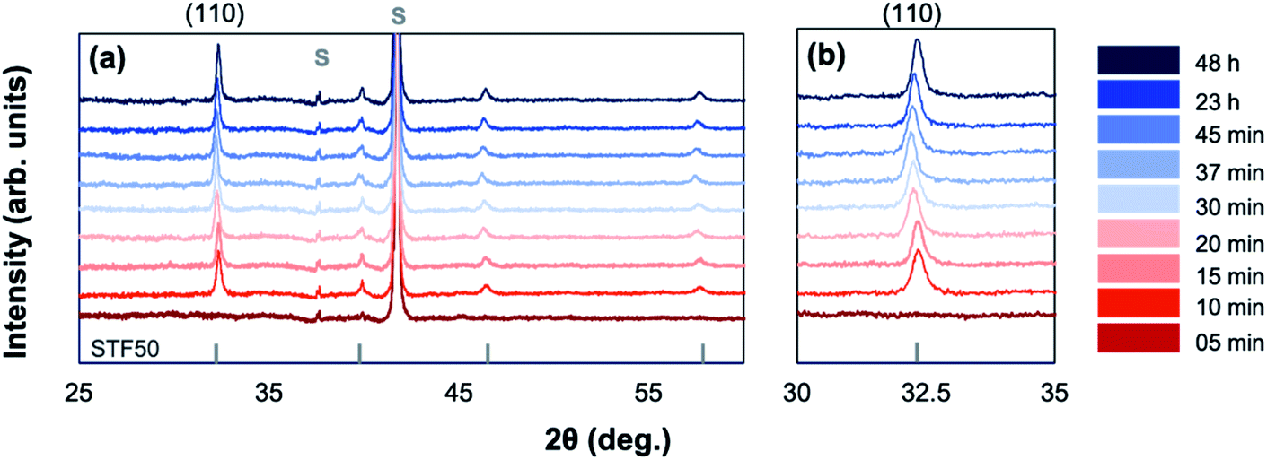 | ||
| Fig. 1 Background-subtracted X-ray diffraction patterns for amorphous-grown STF35 thin films annealed for a series of times along a 400 °C isothermal hold in ∼0.2 atm UHP O2 and ∼0.8 atm UHP Ar. Substrate peaks are marked with an S. Peak positions for STF50 are marked with vertical bars for reference (PDF#97-018-4374). | ||
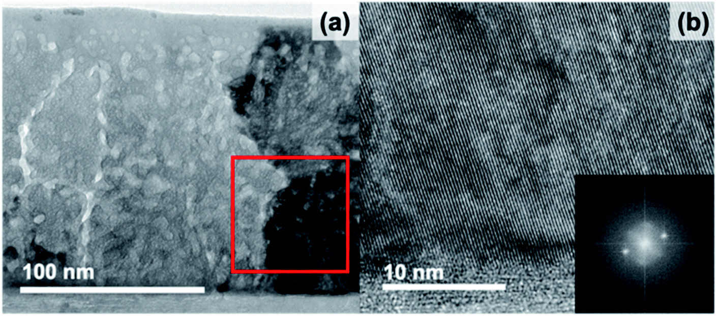
To explore the change in nano- and micro-structure of the films, cross sections for STF35 thin films were studied by transmission electron microscopy (TEM) and scanning transmission electron microscopy (STEM). Bright-field TEM images of STF35 thin films grown amorphous and then annealed are shown for 5 minutes (Fig. 2), 20 minutes (Fig. 3), and 23 hours (Fig. 4) of annealing at 400 °C at different magnifications. Fast Fourier transforms (FFTs) from a region in each film are shown in the insets. Fig. 2 shows that the 5 minute annealed sample is dense and pore-free with uniform mass-thickness contrast at lower magnification (Fig. 2a), but at higher magnification (Fig. 2b) there is a random distribution of bright and dark spots, characteristic of atomic-scale disorder. Additionally, the absence of bright spots and presence of an amorphous ring in the FFT (Fig. 2, inset) indicates the film is non-crystalline and likely of amorphous nature, in agreement with the XRD results (Fig. 1).
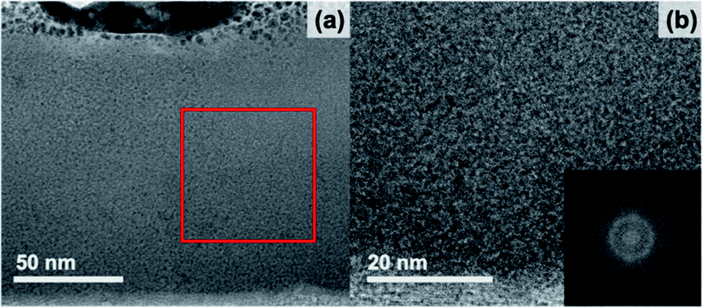 | ||
| Fig. 2 Bright-field TEM images of an amorphous-grown STF35 thin film annealed at 400 °C in ∼0.2 atm UHP O2 and ∼0.8 atm UHP Ar for 5 min at low (a) and high (b) magnification and an FFT (b, inset) of the region outlined by the red box. | ||
 | ||
| Fig. 3 Bright-field TEM images of an amorphous-grown STF35 thin film annealed at 400 °C in ∼0.2 atm UHP O2 and ∼0.8 atm UHP Ar for 20 min at low (a) and high (b) magnification and an FFT (b, inset) of the region outlined by the red box. | ||
 | ||
| Fig. 4 Bright-field TEM images of an amorphous-grown STF35 thin film annealed at 400 °C in ∼0.2 atm UHP O2 and ∼0.8 atm UHP Ar for 23 h at low (a) and high (b) magnification and an FFT (b, inset) of the region outlined by the red box. | ||
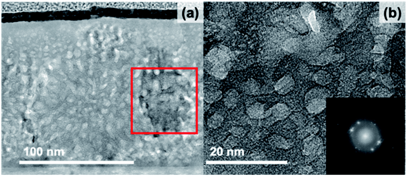
The 20 min annealed sample was characterized using HAADF STEM imaging, EDS mapping, and bright-field TEM imaging. HAADF STEM images of the 20 minute annealed film (Fig. 5) reveal a number of small, regularly distributed, and irregularly shaped dark features. EDS mapping was carried out in the region displayed in Fig. 5b. All peaks in the EDS spectrum were identified, with additional Cu and Ga peaks originating from the TEM grid and FIB preparation, respectively. A line scan, shown in Fig. 5c, was extracted along the red, dashed line in Fig. 5b. As the line scan advances across the dark features, the HAADF intensity (black) decreases, as expected. In the same regions, the Sr, Ti, Fe, and O intensities also decrease while maintaining similar proportions. This result confirms that these features are nano-sized pores, though some do not extend through the entire thickness of the TEM lamella, which accounts for the range in contrast observed. The EDS line scans also demonstrate compositional uniformity in the solid phase of the film 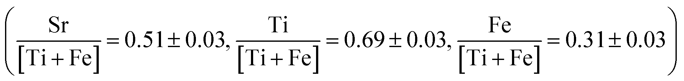 , as verified by spatially-resolved quantitative elemental ratios (not shown). No evidence of enhanced Sr concentrations near pore surfaces was observed. Bright-field TEM images from the 20 minute annealed film are shown in Fig. 3. Surrounded by an amorphous matrix, small crystallites with multiple crystallographic and spatial orientations are observed near the pores. Large, darker regions are also observed each with distinct lattice fringes of a single orientation. The average size of the small crystallites, described by Feret's diameter, is 11 ± 4 nm (N = 33), while the dark crystallites are significantly larger with an average size of 96 ± 36 nm (N = 12), illustrating the wide range of crystallite sizes in the annealed film. Additionally, the large crystallites tend to be more regularly shaped than the small crystallites with an average circularity of 0.72 ± 0.09 compared to 0.36 ± 0.30 of the small crystallites. However, the circularity of the small crystallites may be underestimated because the outline of the lattice fringes is more difficult to identify due to the wide range in contrast in the bright-field images. The average size and circularity of the pores are 13 ± 7 nm and 0.68 ± 0.21 (N = 139), respectively. Though, the average size of both crystallites and pores may be overestimated due to a bias toward larger features when manually identifying features. The FFT (Fig. 3b, inset) shows diffraction spots as well as an amorphous ring, confirming the semi-crystalline state.
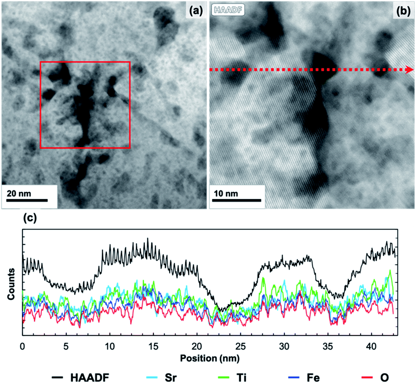 | ||
| Fig. 5 HAADF STEM image of an amorphous-grown STF35 thin film annealed at 400 °C in ∼0.2 atm UHP O2 and ∼0.8 atm UHP Ar for 20 min (a), the EDS mapping region (outlined in red (a)), and line scan path (b), and the HAADF intensity and Sr, Ti, Fe, and O intensities from the EDS line scan (c). | ||
In the bright-field TEM images shown in Fig. 4, the 23 h annealed sample appears quite similar to the 20 minute sample but has a couple of distinct changes. First, the dark, highly crystalline regions have now grown and extend from the substrate to the surface of the film, reflected in an increase of the average large crystallite size to 110 ± 40 nm (N = 18). Additionally, the pores have begun to connect, forming chains, thus increasing the average size to 37 ± 18 nm and decreasing the circularity to 0.31 ± 0.12 (N = 185).
In order to elucidate the effect of crystallization on the local ion environment, X-ray absorption spectroscopy was used to monitor changes in the cation oxidation states and coordination environments. Fig. 6 shows the Fe K-edge (a and b) and Ti K-edge (c and d) XANES spectra of amorphous-grown STF35 thin films annealed for a series of times (from 0 min to 48 h) along the 400 °C isothermal hold. The edge crest is centered near 7130 eV at the Fe K-edge and near 4980 eV at the Ti K-edge. The shape of the edge crests changes from quite broad to sharp after 10 minutes of annealing. Since the edge crest is highly sensitive to the regularity, or periodicity, of the metal–oxygen sublattice,30 this sharpening of the edge crest indicates the onset of long-range crystallographic order for both B-site cations, in agreement with the XRD results. Qualitative observations about the local cation environment can be made from changes in position and intensity of pre-edge features at both Fe and Ti K-edges. The Fe K-edge (Fig. 6b) exhibits two main pre-edge structures, labeled A and B, centered near 7114 eV and 7123 eV, respectively. Similarly, the Ti K-edge (Fig. 6d) displays two main pre-edge features, labeled 1 and 2, centered near 4970 eV and 4976 eV. Features A and 1 are attributed to quadrupolar (1s → 3d) transitions31–36 and features B and 2 to dipolar transitions.30,33,37,38 The intensity of the quadrupolar transition, reflected in the area of peaks A/1, is mainly influenced by the symmetry of individual B-site coordination units. Conversely the dipolar contribution in transition metal oxides arises from the transition of Fe or Ti 1s electrons into the molecular orbital of neighboring polyhedra, meaning the transition is facilitated by bridging oxygen.39 Accordingly, the strength of this transition is related to the alignment of neighboring coordination units.33,37,38Fig. 7 shows that the position (open symbols) of peaks A (a) and 1 (b) increases in energy slightly while the integrated area (closed symbols) of both peaks decreases between 5 and 10 minutes before leveling off. The intensity of the quadrupolar transition is closely related to the symmetry of individual Fe and Ti coordination units.30–36,38 The extensive similarities between the Ti and Fe edges confirms Fe is fully substituted onto the perovskite B-site.
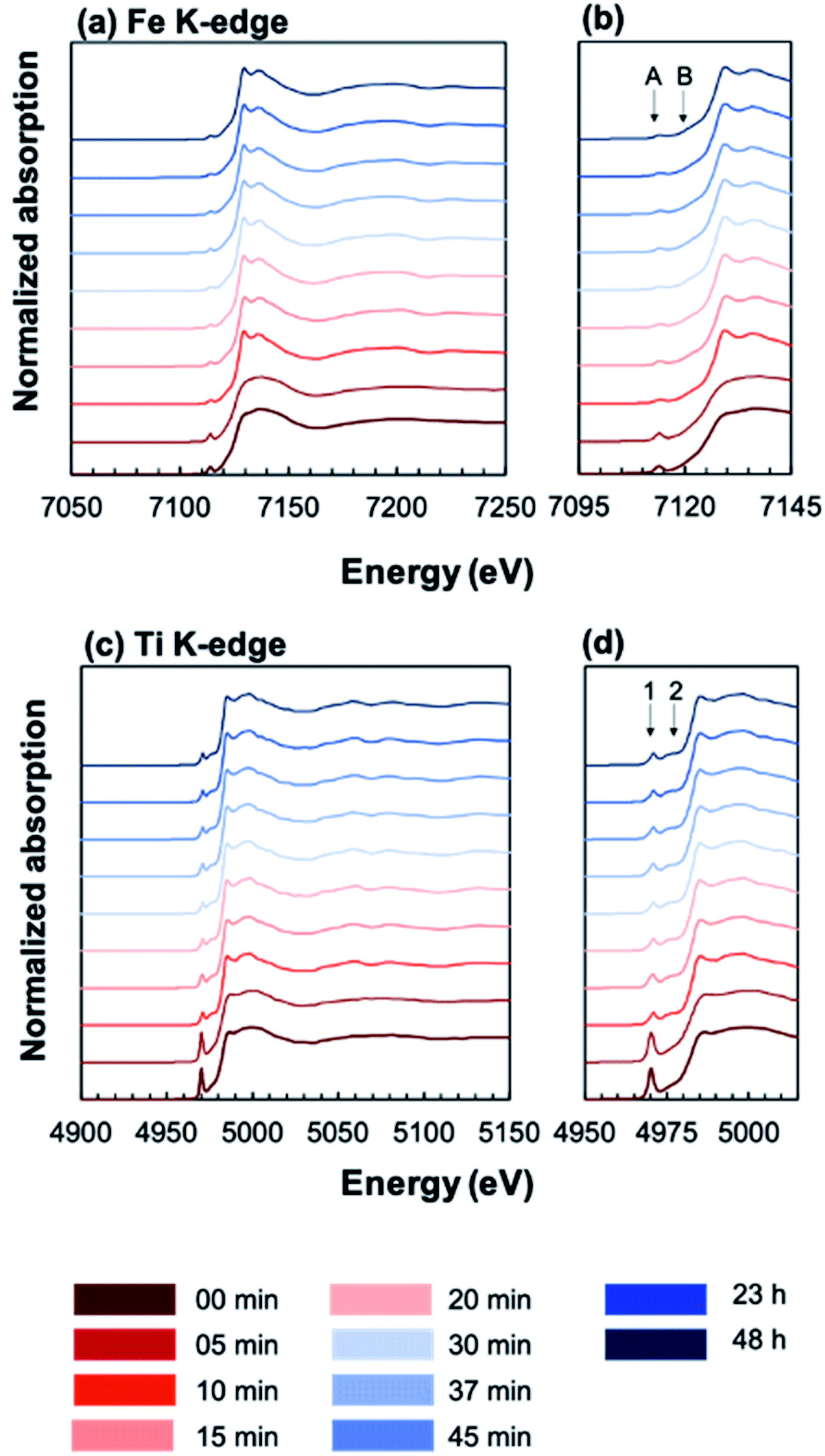 | ||
| Fig. 6 Plot of normalized XANES spectra of annealed, amorphous-grown STF35 thin films at the Fe (a and b) and Ti (c and d) K-edges. Two pre-edge features are labeled with A and B at the Fe K-edge (c) and with 1 and 2 at the Ti K-edge (d). Legend indicates annealing times at 400 °C in ∼0.2 atm UHP O2 and ∼0.8 atm UHP Ar. | ||
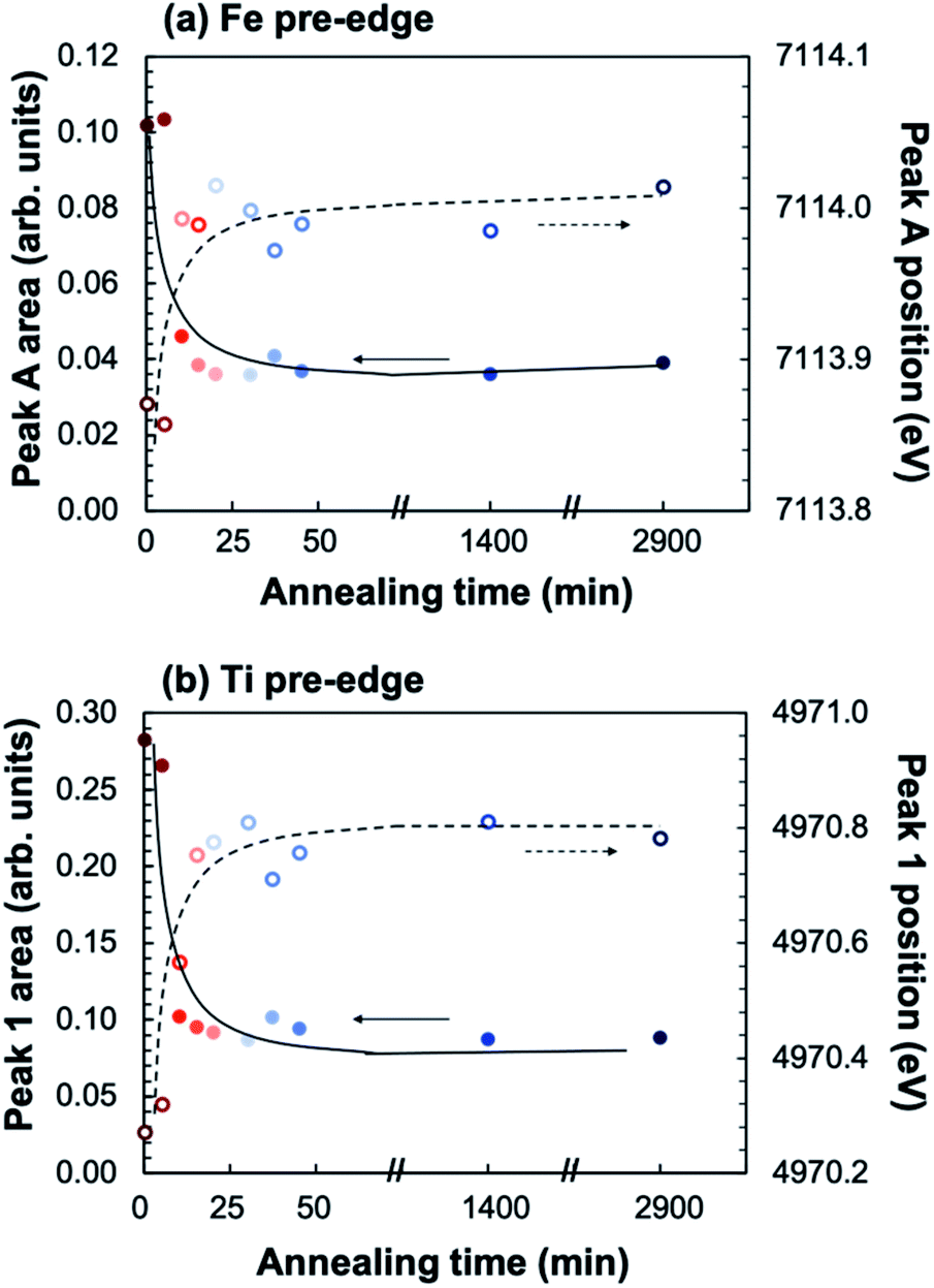 | ||
| Fig. 7 Plot of integrated peak area (closed symbols) and position (open symbols) of pre-edge peaks A at the Fe K-edge (a) and 1 at the Ti K-edge (b) as a function of annealing time at 400 °C in ∼0.2 atm UHP O2 and ∼0.8 atm UHP Ar. | ||
To quantify the Fe oxidation state in the annealed samples, the XANES spectra for three reference iron oxides with known oxidation state (FeO (Fe2+), Fe3O4 (Fe2+/3+), and Fe2O3 (Fe3+)) were measured, showing a linear dependence of the oxidation state on edge position (Fig. 8). The linear trend was interpolated/extrapolated, and the average oxidation state for Fe in each annealed sample was calculated from their edge position. Fig. 8 shows that the Fe oxidation state of the annealed sample increases from ∼2.9 as deposited to ∼3.2 after 10 minutes of annealing, after which it remains relatively constant.
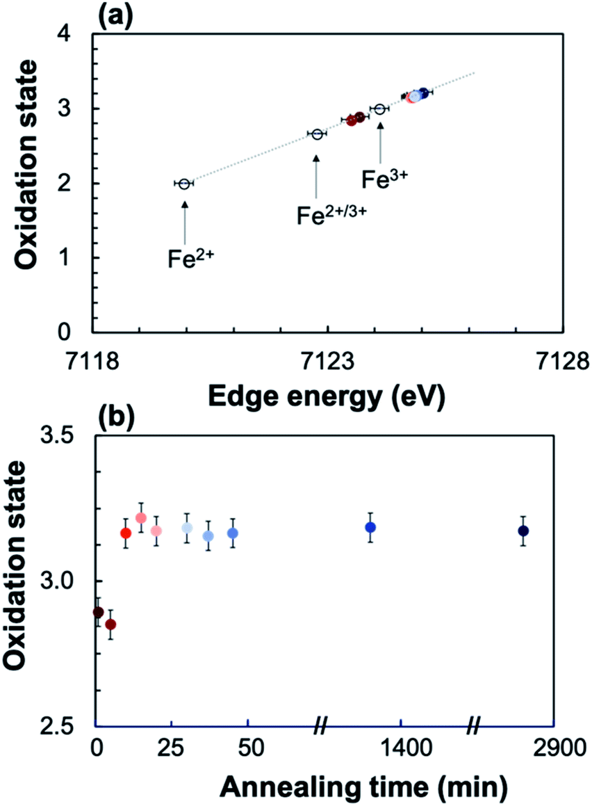 | ||
| Fig. 8 The linear trend between oxidation state and edge energy for FeO (Fe2+), Fe3O4 (Fe2+/3+), and Fe2O3 (Fe3+) was interpolated/extrapolated to calculate the oxidation state of each annealed STF35 sample from the edge position (a). The calculated oxidation state for each STF35 sample is plotted as a function of annealing time at 400 °C in ∼0.2 atm UHP O2 and ∼0.8 atm UHP Ar (b). | ||
Fig. 9a shows select impedance spectra collected along a 400 °C isothermal hold during in situ crystallization of amorphous-grown STF35 thin films, showing the large decrease in resistance as the annealing time increases. The resistance of each arc, extracted from the equivalent circuit fitting, and sample geometry was used to calculate the conductivity. Each impedance spectrum was also analyzed with a DRT approach (Fig. 9b). Here, the actual values of the time constants may be influenced by the parallel capacitance of the substrate as well as by the intrinsic resistive and capacitive film properties. Nonetheless, since the capacitive substrate contribution remains constant, both the distribution and evolution of the relaxation times provide meaningful insight into the film transport behavior during crystallization. At 5 minutes of annealing, there is a peak around ∼1 × 10⁻⁴ s and a very broad, asymmetric tail toward longer relaxation times. This spectrum indicates a range of relaxation times on the slower side, suggestive of widely varying inhomogeneous local transport, with much less variation on the faster side where the peak drops off more sharply. As the annealing time increases to 10 minutes, the primary relaxation peak shifts to shorter (faster) relaxation times, the magnitude of the peak decreases, and the tail becomes less prominent. As crystallization progresses, the distribution of time constants becomes narrower. Fig. 10 shows the evolution of the in-plane conductivity during the in situ crystallization of an amorphous-grown STF35 thin film at 400 °C. As the annealing time increases, the conductivity increases by over two orders of magnitude and gradually plateaus over 48 h, shown in Fig. 10a. Over the first 60 minutes of the anneal, as seen in Fig. 10b, there is a rapid increase in conductivity with a significant decrease in slope between 10 to 20 minutes. After 48 h, the conductivity of the in situ-crystallized film reaches that of a grown-crystalline film on a (0001)-oriented sapphire substrate measured at the same temperature and gas atmosphere,26 shown as a dashed line in Fig. 10.
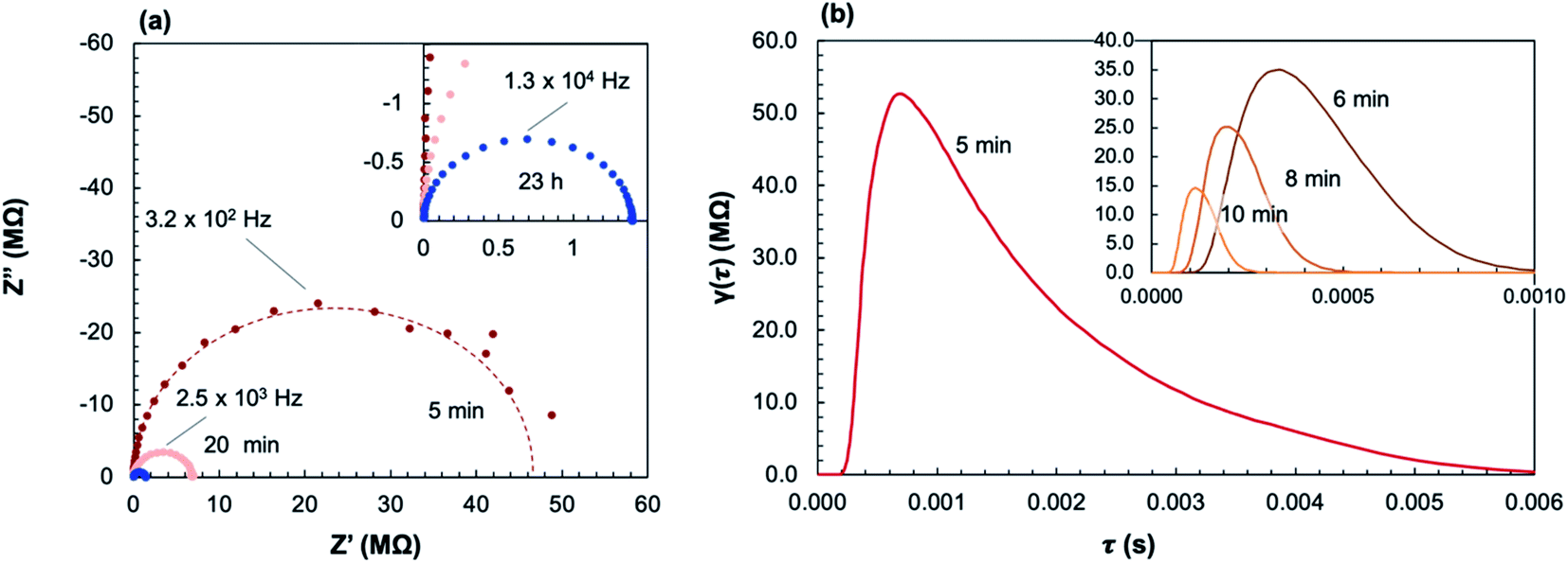 | ||
| Fig. 9 Nyquist plot (a) and DRT spectra (b) of select impedance spectra collected during in situ crystallization at 400 °C in ∼0.2 atm UHP O2 and ∼0.8 atm UHP Ar. | ||
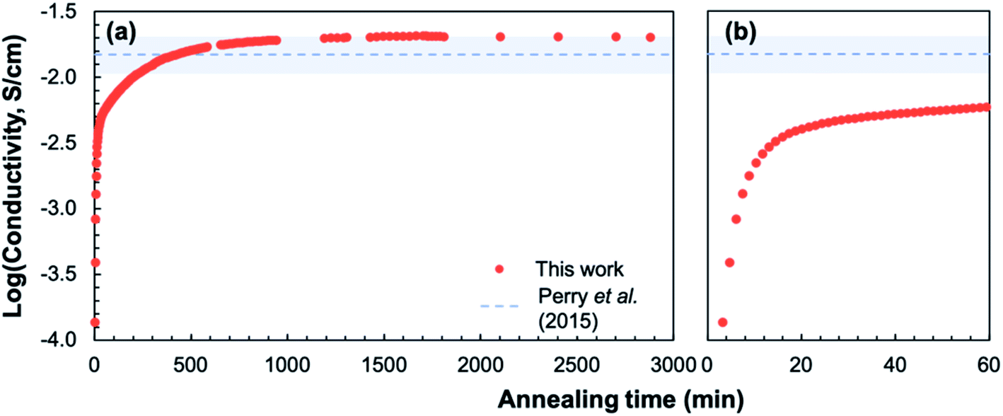 | ||
| Fig. 10 Plot of conductivity over the full annealing period (a) and over the first hour (b) at 400 °C in ∼0.2 atm UHP O2 and ∼0.8 atm UHP Ar; dashed line shows the conductivity and conservative uncertainty estimate (shaded blue) of a crystalline-grown STF35 thin film26 under the same conditions. | ||
To relate the conductivity to the degree of crystallinity, the crystalline volume-percent (vol%) was calculated from the ratio of the integrated peak area to the total area27 from the background-subtracted XRD patterns for each sample (Fig. 11). There are two distinct regions where the dependence of the conductivity on the degree of crystallinity differs. There is an initial increase in conductivity occurring between 1% and 18% crystalline, or between 5 and 10 minutes of annealing. The second large jump in conductivity occurs between 37% and 60% crystalline, where the conductivity of the crystallizing film reaches that of a fully crystalline STF35 thin film on a (0001) oriented sapphire substrate measured under the same conditions.26
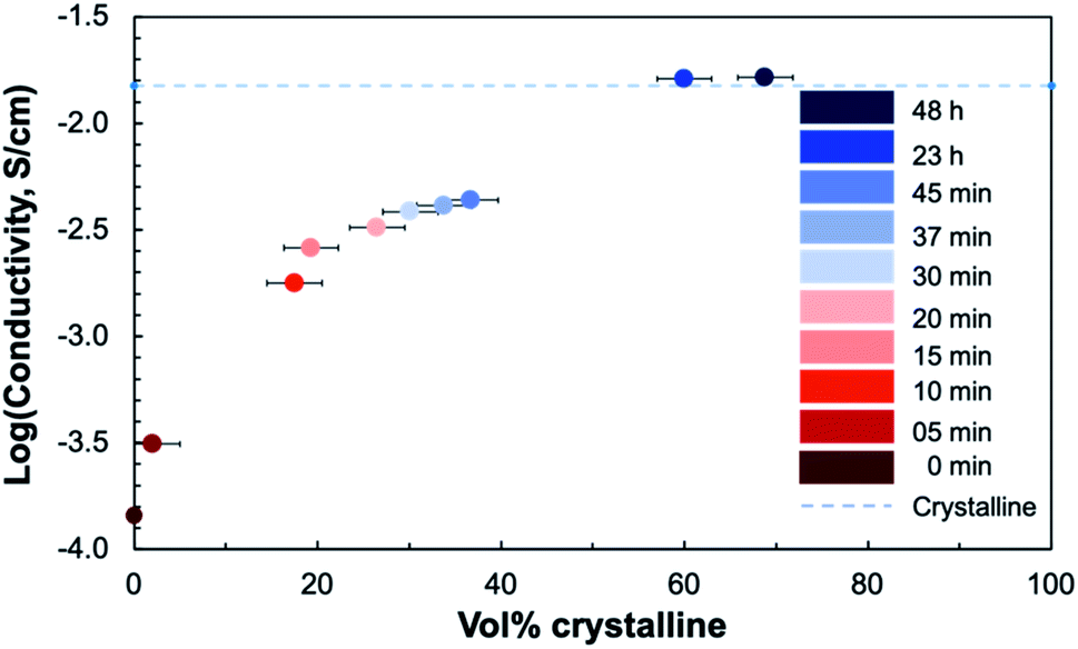 | ||
| Fig. 11 Plot of the logarithmic in-plane total conductivity at 400 °C in ∼0.2 atm UHP O2 and ∼0.8 atm UHP Ar as a function of crystalline volume percent of crystallizing STF35 thin films. The conductivity of a crystalline-grown STF35 thin film, from ref. 26, measured under the same conditions is marked by the dashed line. | ||
4. Discussion
From these results, three main observations are presented. First, oxidation occurs with crystallization, seen from XAS measurements at the Fe K-edge. As STF35 crystallizes, the Fe edge position shifts to higher energies, indicating an increase in Fe oxidation state (Fig. 8). Films annealed over 10 minutes have begun to crystallize (Fig. 1) and have a higher Fe oxidation state compared to amorphous films. This is consistent with previous results18 showing an increase in optical absorption, which is linearly proportional to oxygen content in crystalline films,25 between amorphous and crystallized STF35 thin films, providing further evidence that crystallization occurs with oxygen incorporation. Moreover, these prior results showed that the films' ability to demonstrably exchange oxygen with the gas phase initiates with crystallization; therefore, we expect here also that the oxidation takes place with oxygen incorporation from the gas phase rather than from the solid phase, e.g., by gettering oxygen inhomogeneously from other regions of the film. Despite that expectation, nucleation seems to take place homogeneously rather than at the film–gas interface. We note that this extent of oxidation during post-deposition annealing is unique to the amorphous-grown films during crystallization and does not take place in films grown crystalline at higher temperatures under the same PLD chamber oxygen partial pressure. From chemo-mechanical considerations, this result is not surprising. In MIECs, oxidation and contraction (or reduction and expansion) tend to be coupled. It is therefore consistent that contraction taking place during crystallization would favor oxidation, and that the lower densities of the amorphous films would correspond to a more reduced state initially.Second, chemical changes from oxidation and crystallization drive the multi-scale structural changes in the film, ultimately leading to hierarchical nanostructures. As noted above, as Fe oxidizes, a local contraction is expected, as effective ionic radius generally decreases in the order Fe2+ > Fe3+ > Fe4+ (with small variations due to spin state);40 in crystalline STF, oxidation leads to a smaller lattice parameter.41 Aside from the XAS edge position, the pre-edge features provide additional insight into the cation coordination environment. For Fe and Ti, the relatively low intensity pre-edge peaks A and 1 (Fig. 6c and d) have been attributed to weak electronic quadrupole (1s → 3d) transitions. More than one peak in this region has been reported32,33,42 in the literature due to the crystal field splitting of the 3d orbital energy levels, but the energy resolution of our measurements is too large to resolve separate peaks. Due to selection rules, this transition is completely forbidden when the absorber site symmetry is Oh (full octahedral coordination). However, when inversion symmetry is broken by polyhedral distortions, there is 3d–4p orbital mixing and the quadrupole transition becomes partially allowed, resulting in low intensity peaks in the pre-edge region.30–36,38 Thus, the decrease in intensity, or integrated area, of peaks A and 1 (Fig. 7) observed with increasing crystallinity indicates an increase in symmetry of individual B-site cation coordination units. At the same time, Fe4+ is associated with symmetry-breaking Jahn–Teller distortions of the octahedra.43 These lingering distortions prevent the achievement of perfect symmetry and are evidenced in the non-zero peak A and 1 peak intensity even after long annealing times.
The position of peaks A and 1 has also been empirically related to the average coordination number for both Fe and Ti36,44 through the extensive use of standards. The increase in position of peaks A and 1 (Fig. 7) then suggests an increase in Fe and Ti coordination number with increasing crystallinity, which is consistent with oxidation occurring with crystallization via oxygen incorporation from the gas phase to the lattice. Though the use of only one pre-edge parameter (position or integrated area) is not sufficient to quantify the coordination number,36 the trend of increasing coordination number with increasing peak position still stands.
Features B and 2 are characteristic of dipolar transitions and can arise from metal–metal interactions that are mediated by oxygen bridging.32,33,36 The intensity of this non-local contribution is primarily influenced by the degree of covalency and thus by B–O–B bond angle,45 which affects the degree of orbital overlap between the B-site cation 3d and O-2p orbital, as illustrated in Fig. 12.33 This feature is absent at both Fe and Ti K-edges for the as-deposited and 5 minute-annealed sample, implying a deviation of the B–O–B bond angle from the ideal 180°. After annealing for 10 minutes, these features appear and become slightly more pronounced, providing evidence of increased structural ordering among neighboring B-site polyhedra with crystallization. Increased distortions in the B-site polyhedra from rigid octahedral rotations have been associated with a decrease in the lattice parameter,46 so the observed increase in alignment of neighboring polyhedra, or decrease in distortions, with crystallization could result in an expansion of the lattice. However, other distortions, such as changes in B–O bond length45,46 or polyhedral connectivity,47,48 can occur along with the polyhedral rotations. This, along with the change in coordination environment from oxidation,49,50 convolutes the origin of crystallization-induced strain and results in complex structural changes. In Fig. 1b, an initial decrease in (110) diffraction peak position up to 30 minutes of annealing, followed by an increase of the (110) peak position, is observed. This trend indicates an expansion and subsequent contraction of the (110) lattice parameter of crystalline regions in the film, reflecting the complexity of the induced strains. Similar behavior has been reported by Lubomirsky et al.48 in crystallizing BaTiO3 thin films, and a model is suggested. In that work, it was concluded that upon heating (and thus crystallization), edge-to-edge and face-to-face connections of TiO6 polyhedra are severed and reconnected as corner-sharing connections. This severing of the non-corner-sharing octahedra requires a volume increase, explaining the initial expansion, and the reconnection at the corners results in a volume decrease. This model assumes that the B-site cation remains fully octahedrally coordinated during the transformation, however, which is not observed in the STF35 thin films investigated in this work. Further, the low initial density of amorphous films that we have observed by X-ray reflectivity (not shown) seems inconsistent with high density packing arrangements like face- and edge-sharing polyhedra. Nonetheless, the possibility of evolving polyhedral connectivity cannot be eliminated. We note other researchers12,51 have also described oxide crystallization solely in terms of rearranging polyhedral connectivity rather than in a change in coordination number or in shape of the polyhedra themselves. Our results are inconsistent with that description and suggest an important role of changing coordination symmetry and alignment. It is yet to be seen whether such effects are unique to mixed conductors undergoing oxidation, though we note one similar result to ours in the case of crystallizing transparent oxide semiconductors.47,50 Other possibilities for the crystalline region expansion then contraction are redistribution of oxygen content among the crystalline vs. amorphous regions of the film as crystallization progresses, or temporary tensile strains imposed on crystallites as the surrounding amorphous matrix contracts during crystallization.
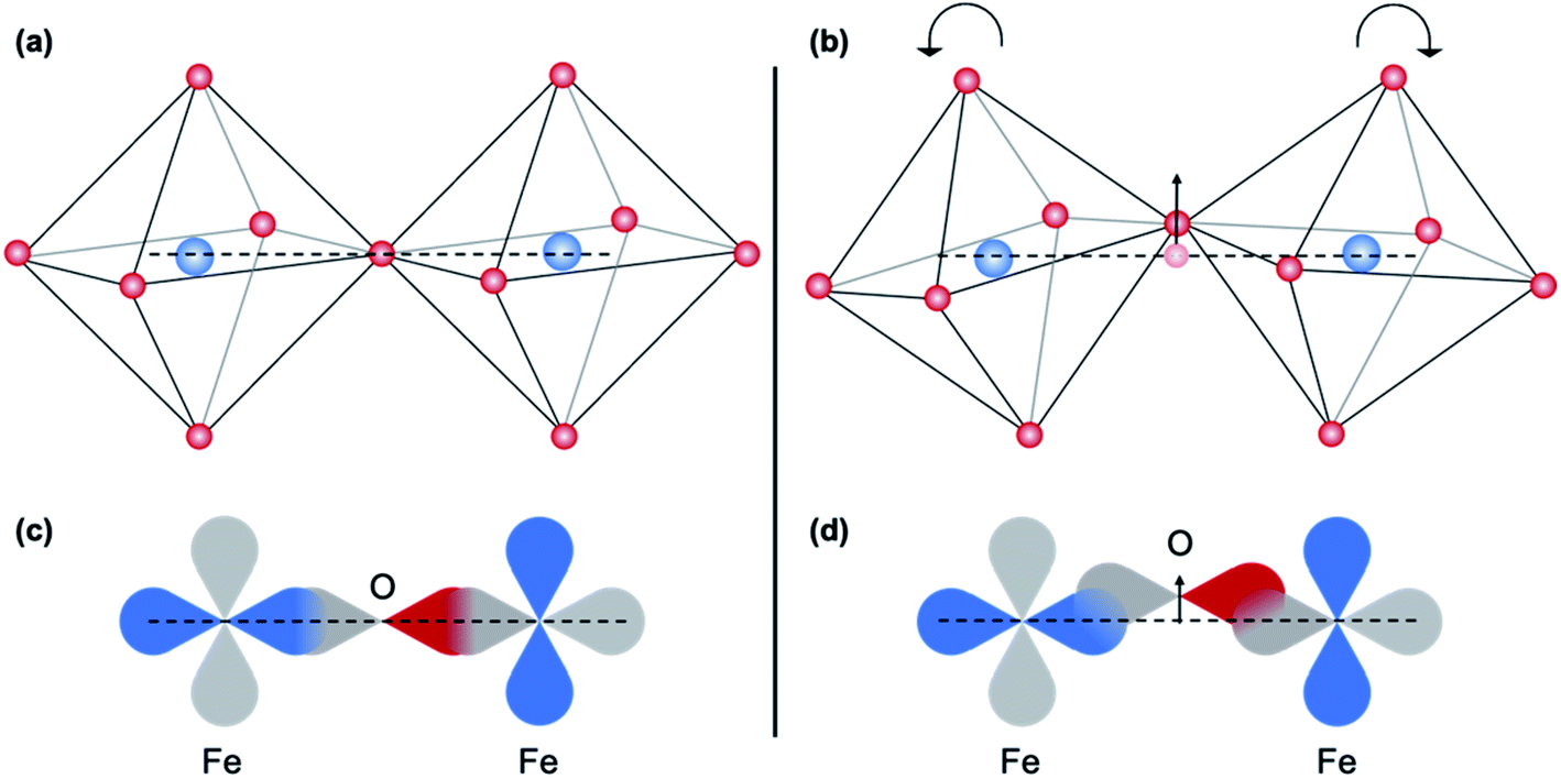 | ||
| Fig. 12 Schematic representation of the effect of the Fe–O–Fe bond angle on the O 2p and Fe 3d orbital overlap. The arrow indicates the change in position of the bridging oxygen. | ||
The presence of the crystallization- and oxidation-induced strain is directly evidenced by the changes in microstructure observed in the electron micrographs (Fig. 2–5). With the onset of crystallization, regularly distributed, isolated pores with an average size of 13 nm appear through the bulk of the annealed STF35 films along with a wide range of crystallite sizes, ranging from 11 to 96 nm. Over time, the average crystallite size increases, and the largest crystallites extend through the thickness of the film from substrate to surface. Additionally, the pores eventually form chains, seemingly located near large crystallites. This would suggest that the pore chains arise from further strain from the growing crystallites, though additional work is required to fully understand the pore-crystallite spatial relationship. Pore chain formation could enable eventual development of open porosity connecting to the film surface, which may benefit surface exchange kinetics. Nano-porosity has been observed in other crystallized (amorphous-deposited) MIEC compositions as well,18,22,23 in some cases with open porosity after higher annealing temperatures. Conversely, no porosity was reported in other crystallized (amorphous-deposited) systems.20,21 This contrast and the evolution of pores seen in the present work suggests that the porosity can be tailored. As noted, the development of open porosity could be beneficial for kchem due to the increase in surface area available for oxygen incorporation.
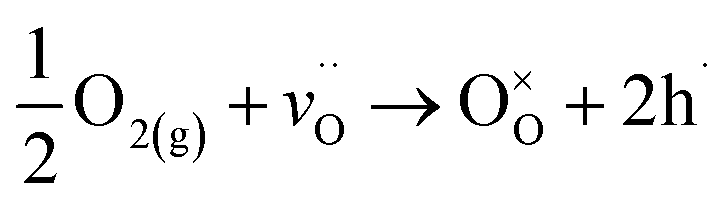
Third, these observed chemical and structural changes from crystallization have implications for the point defect chemistry and electrical behavior. Though the conductivity of the amorphous structure is quite low, as previously reported with other compositions,20,21 the over two-orders-of-magnitude increase in conductivity (Fig. 10) can be explained with the previously observed changes in relation to the hole concentration, hole mobility, and microstructure. Crystalline STF35 is a strongly p-type system under oxidizing conditions, and the electronic conduction occurs through the directional O-2p and Fe-3d orbitals,14 which are partially covalent.25,52 Oxidation produces four holes per oxygen molecule incorporated, which contributes to the increase in hole concentration, according to eqn (2):
 | (2) |
Again, these holes are located in the vicinity of Fe but with some charge sharing with O possible. The increase in symmetry and alignment of B-site coordination units, discussed above, helps to increase the O-2p and Fe-3d orbital overlap, resulting in an increase in hole mobility. However, according to the XAS results, both the increase in hole concentration and mobility occur relatively early on in the crystallization process, most likely tied to the first increase in conductivity between 3% and 20% crystalline (Fig. 11). There is no significant change in polyhedra symmetry or alignment in the later stages of crystallization, indicating that the second increase in conductivity is likely not linked to any further increase in the average covalency of the Fe–O bond. Instead, the second increase in conductivity between 40% and 60% crystalline may be due to microstructural changes, such as the percolation of crystalline grains around 50% crystalline volume fraction. It is possible that grain boundaries play a role, given the small crystallite size and random orientation of crystallites. Grain boundaries in bulk, crystalline, oxidized STF35 are non-blocking to holes,53 but they are blocking in STF with dilute Fe; this difference is attributed to modification of grain boundary space charge layers depending on background hole concentration. Since hole concentration increases relatively early on in the process, we expect grain boundaries to not be significantly blocking in later stages of crystallization. Further microstructural interpretation may be drawn from the DRT analysis (Fig. 9). At 5 minutes of annealing, the broad tail toward slower (longer) relaxations would be somewhat consistent with the presence of blocking grain boundaries prior to full oxidation. However, the shape of a gradually diminishing tail rather than a distinct shoulder is suggestive of very inhomogeneous local transport and a wide distribution of local structures underlying this inhomogeneity. The sharper cutoff on the faster (shorter) relaxation time side suggests that the fast process corresponds to oxidized and well aligned crystalline regions while the slower processes correspond to the wide variety of more reduced, disordered amorphous configurations, possibly also including grain boundaries. This interpretation is consistent with the gradual disappearance of this tail as annealing and crystallization progress, leading to a narrower distribution of time constants expected from more homogeneous crystalline regions, diminishing grain boundary volume fraction, and decrease of grain boundary blocking behavior as oxidation proceeds. Overall, we see evidence for three synergistic contributions to the evolving in-plane conductivity during crystallization: hole concentration, hole mobility, and microstructure.
Our observations of an orders-of-magnitude increase in electronic conductivity can help to explain the dramatic increases in surface exchange coefficients observed in previous work between amorphous and just-crystallized STF35 thin films. In crystalline STF35, the availability of mobile oxygen vacancies,54 the covalency of the Fe–O bond at the surface55, and the ability to transfer charge across the surface54 have been suggested to influence surface oxygen exchange kinetics. As we have observed the films to oxidize during crystallization in this work, the oxygen deficiency decreases with crystallinity, so we do not expect the availability of mobile oxygen vacancies to play a large role in increasing kchemvs. amorphous samples. On the other hand, we have not yet directly measured oxygen mobility as a function of crystallinity. We have surmised an increased covalency of the Fe–O bond from the observed increasing alignment of neighboring B-site polyhedra during crystallization. Our measurements were not strictly surface sensitive, but it seems possible that the enhanced oxygen exchange kinetics for in situ-crystallized vs. amorphous STF may be assisted by the increased covalency of the Fe–O network. Finally, given the very dramatic onset of rapid surface oxygen exchange during crystallization observed in prior studies, we suggest that the orders-of-magnitude increase in (predominantly electronic) conductivity seen in the present work provides the best explanation for the differences in kchem. We have explicitly shown that both the hole concentration and mobility dramatically increase during crystallization, likely boosting the ability to transfer charge at the surface during oxygen exchange. Thus this work helps to explain the differences in kchem for semi-crystalline vs. amorphous films. Explaining the other comparison of kchem, between semi-crystalline (low-temperature-processed) vs. crystalline-grown (high-temperature processed) materials, is beyond the scope of the present work, but based on prior studies18,23 we think the differences in surface chemistry may predominate there; low-temperature-processed mixed conductors lack the same degree of deleterious A-site cation surface segregation.
5. Summary and conclusion
Amorphous STF35 thin films were grown on (0001) oriented Al2O3 substrates. For the ex situ structural characterization, the amorphous films were annealed for a series of times along an isothermal hold to obtain films with varying degrees of crystallinity. The degree of crystallinity was quantified using background-subtracted XRD measurements. The microstructure was imaged using bright-field TEM, HAADF STEM, and EDS mapping, and the local cation environment was evaluated using XAS. The conductivity evolution was monitored in situ using a.c. impedance spectroscopy. From these results, three key findings are presented. First, crystallization occurs with oxidation. There is a rapid increase in Fe oxidation state during annealing of amorphous films as they crystallize. Second, the chemical changes from oxidation and the onset of crystallization facilitate the structural rearrangement on the nano and micro scales. As the films oxidize and crystallize, the B-site cation coordination number increases, the coordination units become more symmetric, and neighboring coordination units become better aligned. The resulting eventual contraction of the solid phase gives rise to hierarchical nanostructures with pores, and the arrangement/connectivity of pores and crystallites evolves during annealing. Last, the chemo-mechanically driven structural evolution and underlying point defect concentration changes have significant implications for the conductivity. Oxidation leads to an increase in hole concentration; the associated increased symmetry and alignment of coordination units increases the hole mobility through O-2p/Fe-3d orbital overlap; and resulting porosity and grain growth influences connectivity of crystalline grains. The combination of oxidation and dynamic nano-structuring from crystallization in STF35 thin films may help to explain the emergence of rapid oxygen surface exchange kinetics during crystallization seen in previous work.18,23 Given the resulting high electronic conductivity, low-temperature processing leading to semi-crystalline hierarchical MIECs exhibits significant promise for developing high performance MIECs for low-to-intermediate temperature applications.Author contributions
HBB: formal analysis, investigation, methodology, supervision (JSG), visualization, writing- original draft. QM: investigation, resources. JSG: investigation. ES: formal analysis. NHP: conceptualization, funding acquisition, methodology, project administration, resources, supervision (HBB, JSG, ES), writing-review & editing.Conflicts of interest
There are no conflicts of interest to declare.Acknowledgements
This work was funded by a DOE Early Career Award to NHP: grant number DE-SC0018963. HBB acknowledges a 3M Graduate Fellowship. XAS measurements were performed at beamline 5-BM-D of DND-CAT, which is supported through E. I. duPont de Nemours & Co., Northwestern University, and Dow Chemical Company. Use of the APS, an Office of Science User Facility operated for the U.S. Department of Energy (DOE) Office of Science by Argonne National Laboratory, was supported by the U.S. DOE under Contract No. DE-AC02-06CH11357. This work was carried out in part in the Materials Research Laboratory Central Research Facilities, University of Illinois. The authors acknowledge the use of facilities and instrumentation supported by NSF through the University of Illinois at Urbana-Champaign Materials Research Science and Engineering Center DMR-1720633.References
- K. Nomura, H. Ohta, A. Takagi, T. Kamiya, M. Hirano and H. Hosono, Nature, 2004, 432, 488–492 CrossRef CAS.
- K. Ide, K. Nomura, H. Hosono and T. Kamiya, Phys. Status Solidi A, 2019, 216, 1800372 CrossRef.
- Z. A. Grady, C. J. Wilkinson, C. A. Randall and J. C. Mauro, Frontiers in Energy Research, 2020, 8, 218 CrossRef.
- J. H. Choi, Y. Mao and J. P. Chang, Mater. Sci. Eng., R, 2011, 72, 97–136 CrossRef.
- S. Koveshnikov, W. Tsai, I. Ok, J. C. Lee, V. Torkanov, M. Yakimov and S. Oktyabrsky, Appl. Phys. Lett., 2006, 88, 022106 CrossRef.
- Y. Aoki, C. Wiemann, V. Feyer, H. S. Kim, C. M. Schneider, H. Ill-Yoo and M. Martin, Nat. Commun., 2014, 5, 3473 CrossRef.
- A. von der Heiden, M. Bornhöfft, J. Mayer and M. Martin, Phys. Chem. Chem. Phys., 2019, 21, 4268–4275 RSC.
- T. Okumura, S. Taminato, Y. Miyazaki, M. Kitamura, T. Saito, T. Takeuchi and H. Kobayashi, ACS Appl. Energy Mater., 2020, 3, 3220–3229 CrossRef CAS.
- J. B. Bates, N. J. Dudney, G. R. Gruzalski, R. A. Zuhr, A. Choudhury, C. F. Luck and J. D. Robertson, Solid State Ionics, 1992, 53, 647–654 CrossRef.
- J. B. Bates, N. J. Dudney, G. R. Gruzalski, R. A. Zuhr, A. Choudhury, C. F. Luck and J. D. Robertson, J. Power Sources, 1993, 43, 103–110 CrossRef CAS.
- S. S. Berbano, M. Mirsaneh, M. T. Lanagan and C. A. Randall, Int. J. Appl. Glass Sci., 2013, 4, 414–425 CrossRef CAS.
- I. Garbayo, M. Struzik, W. J. Bowman, R. Pfenninger, E. Stilp and J. L. M. Rupp, Adv. Energy Mater., 2018, 8, 1702265 CrossRef.
- M. Kuhn, J. J. Kim, S. R. Bishop and H. L. Tuller, Chem. Mater., 2013, 25, 2970–2975 CrossRef CAS.
- A. Rothschild, W. Menesklou, H. L. Tuller and E. Ivers-Tiffée, Chem. Mater., 2006, 18, 3651–3659 CrossRef CAS.
- J. Druce, H. Téllez, M. Burriel, M. D. Sharp, L. J. Fawcett, S. N. Cook, D. S. McPhail, T. Ishihara, H. H. Brongersma and J. A. Kilner, Energy and Environmental Science, 2014, 7, 3593–3599 RSC.
- H. Tellez, J. Druce, T. Ishihara and J. A. Kilner, ECS Trans., 2016, 72, 57 CrossRef CAS.
- J. Druce, T. Ishihara and J. Kilner, Solid State Ionics, 2014, 262, 893–896 CrossRef CAS.
- T. Chen, G. F. Harrington, K. Sasaki and N. H. Perry, J. Mater. Chem. A, 2017, 5, 23006–23019 RSC.
- K. Lankauf, A. Mroziński, P. Błaszczak, K. Górnicka, J. Ignaczak, M. Łapiński, J. Karczewski, G. Cempura, P. Jasiński and S. Molin, Int. J. Hydrogen Energy, 2021, 46(56), 28575–28590 CrossRef CAS.
- J. Januschewsky, M. Ahrens, A. Opitz, F. Kubel and J. Fleig, Adv. Funct. Mater., 2009, 19, 3151–3156 CrossRef CAS.
- A. Cavallaro, S. S. Pramana, E. Ruiz-Trejo, P. C. Sherrell, E. Ware, J. A. Kilner and S. J. Skinner, Sustainable Energy Fuels, 2018, 2, 862–875 RSC.
- A. Evans, J. Martynczuk, D. Stender, C. W. Schneider, T. Lippert and M. Prestat, Adv. Energy Mater., 2015, 5, 1400747 CrossRef.
- T. Chen, G. F. Harrington, J. Masood, K. Sasaki and N. H. Perry, ACS Appl. Mater. Interfaces, 2019, 11, 9102–9116 CrossRef CAS PubMed.
- N. H. Perry, E. J. Skiba and T. Chen, ACS Appl. Mater. Interfaces, 2020, 12, 48614–48630 CrossRef.
- N. H. Perry, N. Kim, E. Ertekin and H. L. Tuller, Chem. Mater., 2019, 31, 1030–1041 CrossRef CAS.
- N. H. Perry, D. Pergolesi, S. R. Bishop and H. L. Tuller, Solid State Ionics, 2015, 273, 18–24 CrossRef CAS.
- I. C. Madsen, N. V. Y. Scarlett and A. Kern, Zeitschrift für Kristallographie, 2011, 226, 944–955 CrossRef CAS.
- B. Ravel and M. Newville, J. Synchrotron Radiat., 2005, 12, 537–541 CrossRef CAS.
- T. H. Wan, M. Saccoccio, C. Chen and F. Ciucci, Electrochim. Acta, 2015, 184, 483–499 CrossRef CAS.
- F. Farges, J. Non-Cryst. Solids, 2006, 204, 53–64 CrossRef.
- G. A. Waychunas, M. J. Apted and G. E. Brown, Phys. Chem. Miner., 1983, 10, 1–9 CrossRef CAS.
- F. de Groot, G. Vankó and P. Glatzel, J. Phys.: Condens. Matter, 2009, 21, 104207 CrossRef.
- D. Phuyal, S. Mukherjee, S. K. Panda, G. J. Man, K. Simonov, L. Simonelli, S. M. Butorin, H. Rensmo and O. Karis, J. Phys. Chem. C, 2021, 125, 11249–11256 CrossRef CAS.
- Z. Wu, M. Bonnin-Mosbah, J. P. Duraud, N. Métrich and J. S. Delaney, J. Synchrotron Radiat., 1999, 6, 344–346 CrossRef CAS.
- G. A. Waychunas, Am. Mineral., 1987, 72, 89–101 CAS.
- F. Farges, G. E. Brown and J. J. Rehr, J. Phys. IV, 1997, 56, 1809 CAS.
- F. Farges, G. E. Brown and J. J. Rehr, Geochim. Cosmochim. Acta, 1996, 60, 3023–3038 CrossRef CAS.
- L. A. Grunes, Phys. Rev. B: Condens. Matter Mater. Phys., 1983, 27, 2111 CrossRef CAS.
- R. v. Vedrinskii, V. L. Kraizman, A. A. Novakovich, P. v. Demekhin and S. v. Urazhdin, J. Phys.: Condens. Matter, 1998, 10, 9561 CrossRef CAS.
- R. D. Shannon, Acta Crystallogr., Sect. A: Cryst. Phys., Diffr., Theor. Gen. Crystallogr., 1976, 32, 751–767 CrossRef.
- N. H. Perry, J. J. Kim, S. R. Bishop and H. L. Tuller, J. Mater. Chem. A, 2015, 7, 3602–3611 RSC.
- W. Phoohinkong, K. Boonyarattanakalin, W. Mekprasart, S. Pavasupree and W. Pecharapa, Radiat. Phys. Chem., 2020, 174, 198919 CrossRef.
- M. Vračar, A. Kuzmin, R. Merkle, J. Purans, E. A. Kotomin, J. Maier and O. Mathon, Phys. Rev. B: Condens. Matter Mater. Phys., 2007, 76, 174107 CrossRef.
- M. Wilke, F. Farges, P. E. Petit, G. E. Brown and F. Martin, Am. Mineral., 2001, 86, 714–730 CrossRef CAS.
- A. Cammarata and J. M. Rondinelli, J. Chem. Phys., 2014, 141, 114704 CrossRef PubMed.
- E. G. Rini, A. Paul, M. Nasir, R. Amin, M. K. Gupta, R. Mittal and S. Sen, J. Alloys Compd., 2020, 830, 154594 CrossRef CAS.
- S. L. Moffitt, Q. Zhu, Q. Ma, A. F. Falduto, D. B. Buchholz, R. P. H. Chang, T. O. Mason, J. E. Medvedeva, T. J. Marks and M. J. Bedzyk, Adv. Electron. Mater., 2017, 3, 1700189 CrossRef.
- D. Ehre, H. Cohen, V. Lyahovitskaya, A. Tagantsev and I. Lubomirsky, Adv. Funct. Mater., 2007, 17, 1204–1208 CrossRef CAS.
- S. R. Bishop, D. Marrocchelli, C. Chatzichristodoulou, N. H. Perry, M. B. Mogensen, H. L. Tuller and E. D. Wachsman, Annu. Rev. Mater. Res., 2014, 44, 205–239 CrossRef CAS.
- D. E. Proffit, Q. Ma, D. B. Buchholz, R. P. H. Chang, M. J. Bedzyk and T. O. Mason, J. Am. Ceram. Soc., 2012, 95, 3657–3664 CrossRef CAS.
- A. I. Frenkel, D. Ehre, V. Lyahovitskaya, L. Kanner, E. Wachtel and I. Lubomirsky, Phys. Rev. Lett., 2007, 99, 215502 CrossRef PubMed.
- N. Kim, N. H. Perry and E. Ertekin, Chem. Mater., 2019, 31, 233–243 CrossRef CAS.
- J. R. Jurado, M. T. Colomer and J. R. Frade, Solid State Ionics, 2001, 143, 251–257 CrossRef CAS.
- W. Jung and H. L. Tuller, Adv. Energy Mater., 2011, 1, 1184–1191 CrossRef CAS.
- D. N. Mueller, M. L. MacHala, H. Bluhm and W. C. Chueh, Nat. Commun., 2015, 6, 6097 CrossRef CAS PubMed.
| This journal is © The Royal Society of Chemistry 2022 |