
Silicon nanowire–Ta2O5–NGQD heterostructure: an efficient photocathode for photoelectrochemical hydrogen evolution†
Sk
Riyajuddin
 a,
Jenifar
Sultana
a,
Shumile Ahmed
Siddiqui
a,
Sushil
Kumar
a,
Damini
Badhwar
a,
Shyam Sundar
Yadav
b,
Saveena
Goyal
a,
Ananth
Venkatesan
b,
Suvankar
Chakraverty
a and
Kaushik
Ghosh
*a
a,
Jenifar
Sultana
a,
Shumile Ahmed
Siddiqui
a,
Sushil
Kumar
a,
Damini
Badhwar
a,
Shyam Sundar
Yadav
b,
Saveena
Goyal
a,
Ananth
Venkatesan
b,
Suvankar
Chakraverty
a and
Kaushik
Ghosh
*a
aInstitute of Nano Science & Technology, Knowledge City, Sector-81, SAS Nagar, Mohali, Punjab 140306, India. E-mail: kaushik@inst.ac.in
bIndian Institute of Science Education and Research, Knowledge City, Sector-81, SAS Nagar, Mohali, Punjab 140306, India
First published on 18th November 2021
Abstract
Photoelectrochemical (PEC) water splitting has propelled broader research interest for the large-scale and facile entrapment of solar energy in hydrogen fuel. It offers the most favorable and environment-friendly approach to harvest renewable energy under solar radiation for solar-to-hydrogen fuel conversion. However, for superior hydrogen evolution reaction (HER) and enhanced overall efficiency, it is inevitable to design a suitable low-cost, active, scalable and durable photocathode. Although silicon (Si) is the backbone of the photovoltaic industry, an alternate drive is under development to establish its applicability towards PEC-HER. Nevertheless, bare Si with a metal catalyst suffers due to its instability, high reflectance loss, surface oxidation, and sluggish kinetics. These issues can be addressed by passivating the Si surface with the appropriate protection layer anchored with a low-cost metal-free catalyst to design the pertinent photocathode. Herein, vertically aligned p-silicon nanowires (p-SiNWs) with a conformal coating of tantalum pentoxide (Ta2O5) passivation layer and N-doped graphene quantum dots (NGQD) as a metal-free catalyst (p-SiNWs–Ta2O5–NGQD) have been designed, which impart efficient, stable, and scalable photocathodes for PEC-HER. The photocathode exhibits an applied bias photon-to-current conversion efficiency (ABPE) of ∼21.1%, which is 6-fold higher than that of the p-SiNWs–NGQD matrix with a low overpotential (−449 mV @ 5 mA cm−2) and Tafel slope (78 mV dec−1) indicating the superiority of the catalyst. The role of Ta2O5 is not only to act as the passivation layer via reducing the lattice mismatch but it also facilitates the charge transfer process from Si to the electrolyte, minimizing the conduction band offset. Moreover, the non-corrosive nature of NGQD, having various N-functionalities, significantly enhances the active site densities and thereby imparts prolonged durability towards the HER performance for at least 10 hours @ 10 mA cm−2 with negligible potential loss. The simplistic and compatible design strategy can promote a new-fangled pathway for the commercialization of large-scale Si-based metal-free photocathodes towards next-generation green fuel technology.
Introduction
Presently, the majority of energy produced worldwide is accomplished by fossil fuels. The rising energy demands and the restricted supply of conventional energy sources have elevated the fear and nervousness regarding the competence of fossil fuels to uphold the regular energy demands.1–3 In this context, owing to the fast growth of the world population and energy demand, the universal scientific community is forced to pursue the development of alternative clean energy resources to cope-up with the future energy challenges.1–4 Compared to all clean energy resources (wind energy, tidal energy, bioenergy, etc.), sunlight is an abundant source of energy because of its availability and non-hazardous nature.4 In addition, the amount of solar energy reaching the earth's surface is roughly 10![[thin space (1/6-em)]](https://www.rsc.org/images/entities/char_2009.gif) 000 times the total world energy consumption,5 so its conversion to electricity has become a highly attractive and economical process for providing clean and renewable energy for the present and future, which is termed as solar-driven green fuel technology. Photoelectrochemical (PEC) water splitting has emerged as an efficient technology for producing hydrogen using renewable sources like sunlight and water.6,7 Hydrogen has been projected as an imperative source of green fuel because of its high energy density and it can be converted to power upon demand through fuel cells.8,9 However, to be competitive with the renewable energy sources and for large-scale solar-hydrogen production, there is an urgent need to develop low-cost, stable and highly efficient photoelectrodes.2 Since it involves the absorption of light, charge carrier generation, separation, and collection via its facile transfer through a chemical medium, the choice of photoelectrodes is very crucial for enhancing the stability and efficiency of the PEC devices. Simultaneously, the suitability of the band-gaps of active materials for adequate broadband light absorption, the energetic feasibility of the energy band edges for efficient water electrolysis, electrode durability, and the overall cost of fabrication are a few major limitations to the commercialization of PEC technology on a global scale.10 Moreover, water splitting is not a spontaneous process because it requires a minimum of 1.23 V potential for triggering the process.10,11 Thus, the band edges should straddle the redox potential of water splitting. The material must also be stable enough under harsh aqueous operating conditions. Therefore, the main challenge lies in the development of efficient, reliable and cheap photoelectrodes towards green fuel synthesis to support hydrogen fuel-cell technology.
000 times the total world energy consumption,5 so its conversion to electricity has become a highly attractive and economical process for providing clean and renewable energy for the present and future, which is termed as solar-driven green fuel technology. Photoelectrochemical (PEC) water splitting has emerged as an efficient technology for producing hydrogen using renewable sources like sunlight and water.6,7 Hydrogen has been projected as an imperative source of green fuel because of its high energy density and it can be converted to power upon demand through fuel cells.8,9 However, to be competitive with the renewable energy sources and for large-scale solar-hydrogen production, there is an urgent need to develop low-cost, stable and highly efficient photoelectrodes.2 Since it involves the absorption of light, charge carrier generation, separation, and collection via its facile transfer through a chemical medium, the choice of photoelectrodes is very crucial for enhancing the stability and efficiency of the PEC devices. Simultaneously, the suitability of the band-gaps of active materials for adequate broadband light absorption, the energetic feasibility of the energy band edges for efficient water electrolysis, electrode durability, and the overall cost of fabrication are a few major limitations to the commercialization of PEC technology on a global scale.10 Moreover, water splitting is not a spontaneous process because it requires a minimum of 1.23 V potential for triggering the process.10,11 Thus, the band edges should straddle the redox potential of water splitting. The material must also be stable enough under harsh aqueous operating conditions. Therefore, the main challenge lies in the development of efficient, reliable and cheap photoelectrodes towards green fuel synthesis to support hydrogen fuel-cell technology.
Among all the existing semiconductors, silicon has attracted the attention of the global research community because of its suitability as an efficient photocathode in direct solar-driven water splitting due to its energetically favorable band edge positions, low carrier recombination velocity, high carrier mobility, earth abundance, low cost, and environmentally gracious nature.12,13 Despite these advantages, the Si-based PEC devices are still not flourishing because of their instability due to surface oxidation under harsh chemical environments, high reflectance loss and lethargic charge-transfer kinetics at the Si/electrolyte interface owing to small exchange current density, which renders its applicability in the PEC-HER process.12,14 To overcome the stability issues several approaches have been adopted such as the incorporation of a thin-film protection/passivation layer, surface functionalization, variation of the electrolyte medium, etc.11,12,15 The charge transfer kinetics are addressed via modifying the electrode surfaces by anchoring with a suitable electrocatalyst.11,16 In this context, heterojunctions with various metal or metal oxide/sulphide/phosphide-based electrocatalysts have been investigated, which not only protect the silicon surface but they also act as a suitable catalyst.15,17–20 However, these systems suffer from the drawback of attaining high efficiencies because of the lattice mismatch at the Si/metal or Si/metal composite interfaces and therefore create high interfacial barrier resistance. In general, the protective layer should have minimal band offset and high-quality interface with low lattice mismatch to enhance charge carrier collection.21,22
It has been reported that the use of a suitable electrocatalyst and/or semiconducting passivation layer can protect the surface corrosion under operational PEC conditions, which can help to improve the stability and lifetime of the photoelectrodes.23 Recently, Esposito et al.22 demonstrated a noteworthy improvement in the PEC performance of Si-based photoelectrodes by introducing a high-quality thermally grown SiO2 layer and bilayer metal catalyst. However, the large conduction band offset at the Si/SiO2 interface inhibited the charge transfer mechanism. There are also several reports on using different transition metal-oxides as hole-selective (molybdenum oxide, tungsten oxide, vanadium oxide and cuprous oxide, etc.) or electron-selective layers (titanium oxide, tantalum oxide and zinc oxide, etc.) with Si and different metal-based catalysts for PEC application.24–26 Li Ji et al.21 proposed the thin epitaxial layer of STO over Si with Ti/Pt as a nanostructured catalyst that can demonstrate a photocurrent density of −35 mA cm−2 and applied bias photon to current conversion efficiency (ABPE) of 4.9% because of a low lattice mismatch of ∼1.69% (Si-3.84 Å and STO-3.905 Å). Nevertheless, it has been observed that coating the Si surface with TaOx surprisingly enhances the ABPE to 7.7% of the Si/TaOx–Pt system due to a low conduction band offset.24 Inspired by this concept, Wang et al.27 demonstrated a current density of −34.7 mA cm−2 with an ABPE efficiency of 8.1% by using the pn+-Si/Ta2O5/Pt photoelectrode. They realized that Ta2O5 is a better choice as an oxide protection layer for Si because of its very low lattice mismatch of ∼1% at the Si (3.84 Å) and Ta2O5 (3.80 Å) interface; it simultaneously enables the proficient transport of electrons from Si to Ta2O5 due to a very small conduction band offset, and restrains the flow of holes for a large valence band offset. Besides the modification of the interfacial lattice parameters, as well as engineering the band off-set, another alternate approach can be adopted to enhance the efficiency of the Si-based photocathode via the nano-texturing of the Si surface responsible for high photo-absorption. Currently, 1D nanowires are gaining more attention due to high surface to volume ratio, orthogonalization and anti-reflective properties, thereby allowing efficient catalyst loading at a given active area of the Si-based photoelectrode.12,13,16,28
Nevertheless, metal-based PEC-HER catalysts suffer from surface poisoning, high activation barrier, high cost, non-durability, and low efficiency, which have inhibited their commercialization.12,14 In this regard, to surpass the adverse effects of using metal catalysts, researchers are more inclined towards metal-free catalysts like r-GO,29 graphene quantum dots (GQD),16,30 nitrogen-doped graphene quantum dots (NGQD),12,31 graphene sheets,32etc. Among them, NGQD has emerged as an innovative class of materials owing to their large surface areas, high electron mobility, sharp catalytic edges, environmental friendliness, corrosion-resistant properties, excellent transmittance, and tunable band-gap.12,31 Moreover, their discrete electronic levels allow efficient charge transfer and prolong the excited state lifetime, making them suitable catalysts for PEC applications.11,33 In addition, nitrogen functionality facilitates a resistance-less path for the rapid electron transfer process and consequently accelerates the HER kinetics.12,34 Sim et al.31,32 demonstrated the use of N-doped graphene as a catalyst for both planar and nanostructured Si and reported an ABPE of 2.29%. Furthermore, the large band-gap of NGQD enables its absorption in the UV region making it a suitable material for heterojunctions with Si having NIR absorption thus enabling broadband absorption. Along with this, the configuration of the Si-nanowire/passivation layer/catalyst is capable of demonstrating excellent photoelectrochemical performance with substantial improvement of the lifetime of Si-based photoelectrodes. The bifunctional nature of the catalyst not only helps to improve the catalytic performance but also acts as a potential passivating layer to protect the surface oxidation of silicon in harsh media.35,36
Taking into consideration the advantages of Si nanowires coupled with Ta2O5 and NGQD, the present report demonstrates the investigation of p-SiNWs/Ta2O5/NGQD as an efficient photocathode for the PEC-HER. The photocathode exhibits a photocurrent density of −49.5 mA cm−2 along with ABPE of ∼21.1%. The lower values of the overpotential and Tafel slope also indicate the superiority of the catalyst with prolonged stability for at least 10 hours @ 10 mA cm−2 with a loss of ∼5% potential. The as-designed photocathode provides a green route with tandem architecture incompatible with Si-process line technology to facilitate broad-band solar absorption for solar-to-hydrogen fuel conversion.
Experimental section
Fabrication of vertically aligned silicon nanowires (SiNWs)
The nanowires were grown on 1 × 1 cm2 p-type Si 〈100〉 substrates (B-doped; 1–3 Ω cm) via employing a cost-effective nanosphere lithography technique, followed by metal-assisted chemical etching (MACE), as reported elsewhere.37 In brief, the organic impurities of the Si wafers were cleaned by sonication in acetone and ethanol, followed by purified deionized water (DI). The partially cleaned Si substrates were immersed in piranha solution (H2SO4:H2O2 in 3:1 ratio) at 90 °C for an hour, followed by rinsing in DI water and dried using a nitrogen gun. Thereafter, the polystyrene (PS) beads were used as a hard mask for the formation of Si nanowires. The solution of PS beads with ethanol in a 1:1 ratio was sonicated for 2 hours and the solution was slowly transferred over a mixture of DI water and IPA (50:0.002) in a glass Petri-dish to get uniform coverage of the monolayer PS beads. This free-floating hexagonally oriented monolayer film was transferred over the previously cleaned Si substrate. The diameters of the closely packed PS beads were reduced from 450 nm to ∼230 nm by etching under optimized O2 plasma, and 30 nm gold (Au) thin film was deposited by an e-beam deposition technique to catalyze the growth of SiNWs. The protected PS beads were removed under mild sonication in toluene to develop uniform Au mesh on the silicon surface. The resulting Au/Si samples were immersed in HF:H2O2:H2O (1:0.5:5) for 5 minutes to etch the Si underneath, followed by the removal of the Au catalyst in aqua-regia (nitric acid:hydrochloric acid in 1:3), and finally resulted in the formation of uniform vertically aligned p-SiNWs.
Deposition of Ta2O5 on p-SiNWs by the PLD method
The as-prepared vertically aligned p-SiNWs were coated with the thin film of Ta2O5 at a variable thickness by a pulse laser deposition (PLD) system. During deposition, the distance between the target and Si substrate was fixed at 6 mm with the substrate being heated at 350 °C. The deposition was carried out under an oxygen pressure of 1.6 × 10⁻⁶ torr and the rate of deposition was fixed at 0.25 Å per pulse. The laser fluence was optimized and kept at 2 J cm−2 to avoid droplet formation on the film surface.Fabrication of nitrogen-doped graphene quantum dots (NGQD)
N-doped graphene quantum dots (NGQD) were synthesized by the pyrolysis of citric acid as reported elsewhere.38 Briefly, 3 g of citric acid were heated at 200 °C for 20 minutes to obtain an orange-coloured liquid. Then, 0.25 mol L−1 NaOH solution was slowly added dropwise into 100 mL of the earlier obtained orange-coloured solution under rigorous stirring until pH ∼ 7. A change in colour from orange to brown and finally faint yellow (almost transparent) indicated the formation of GQD. Thereafter, 10 mL of the as-prepared GQD was mixed with 10 mL of a 6.5 M aqueous solution of urea under constant stirring for 30 minutes, followed by heating at 110 °C for 3 hours in a poly-tetra-fluoro-ethylene-lined autoclave. After cooling to room temperature, an orange homogeneous solution of NGQD was obtained. This solution was then centrifuged for 15 minutes at 10000 rpm to remove any undissolved materials. The supernatant was further filtered through a 0.22 μm cellulose acetate membrane to remove larger particles and the remaining filtrate containing the desired NGQD was processed for necessary characterization.
Material characterization
The as-prepared samples were physically characterized by employing Field Emission Scanning Electron Microscopy (FE-SEM), (JEOL JSM-7600F) and Transmission Electron Microscopy (TEM) (JEOL JEM 2100) operated at 200 kV for the morphological and structural investigations. The optical properties of NGQD were investigated using a Shimadzu UV-Vis spectrometer (model UV-2600) and the PL spectra were recorded on a FluoroLog 3-221 (HORIBA Scientific) fluorimeter equipped with a 450 W xenon lamp. To investigate the surface functionalization of the NGQD and GQD, Attenuated Total Reflectance Fourier Transform Infrared (ATR-FTIR) spectroscopy (Thermo Scientific Nicolet iS5) was used. The as-prepared NGQD was also analyzed by Confocal Raman Microscopy (WITEC alpha 300R Raman spectrometer with a 532 nm Nd-YAG laser with 1800-line mm−1 grating) and the size of the as-prepared NGQD was determined by Atomic Force Microscope (AFM) analysis in tapping mode under ambient conditions using a BRUKER multimode 8 AFM. The powder X-ray diffraction (PXRD) studies were carried out using Cu Kα radiation (BRUKER, ecoD8 ADVANCE) to investigate the crystalline structure and phase of the deposited materials on the surface of p-SiNWs. To investigate the impregnation of NGQD on the surface of p-SiNWs–Ta2O5, X-ray Photoelectron Spectra (XPS) (EscaLab: 220i-XL) were obtained with a monochromatized Mg Kα energy source (1253 eV).Fabrication of the photocathode for photoelectrochemical measurements
The as-prepared p-SiNWs–Ta2O5 sample was coated with NGQD by drop-casting a 400 μL solution of NGQD and Nafion (5:1) (each with 100 μL in a time interval of 40 minutes) followed by drying under an IR lamp for 2 hours. The as-prepared final samples p-SiNWs–Ta2O5–NGQD acted as the main working electrode for PEC measurement. The back side of the electrode, which was connected with the copper wire, was covered by the insulating polymer adhesive to avoid any shorting or electrocatalytic contribution from the backside of the Si-chip. The measurements were carried out in a three-electrode electrochemical workstation (Metrohm-Autolab PGSTAT302N). A double junction Ag/AgCl electrode saturated with 3 M KCl was used as a reference electrode (Metrohm) and Pt wire was taken as the counter electrode (Metrohm). Prior to the electrochemical measurements, the electrodes were rinsed several times with DI water and dried with compressed air. The distance between the working and reference electrodes was kept fixed (∼1 cm) for every electrochemical analysis. For the irradiation source of the PEC-HER reaction, a xenon lamp (AM 1.5 G filter) calibrated at a power of 100 mW cm−2 was kept at a distance of 5 cm from the quartz cell reactor. The PEC-HER activity of the as-prepared photocathode was investigated via linear sweep voltammetry (LSV) with a scan rate of 5 mV s−1 under both illuminated and dark conditions. Chronopotentiometric measurements were carried out at an applied current density of 10 mA cm−2 for at least 10 hours in a 1 M HClO4 electrolyte solution. The electrochemical impedance analysis (EIS) was performed at an applied voltage of −300 mV (vs. RHE) over a frequency range from 100 kHz to 0.01 Hz with an AC amplitude of 10 mV in a three-electrode system. All electrochemical analyses were carried out in 1 M HClO4 electrolyte solution and applied potentials were converted in terms of the reversible hydrogen electrode (RHE) using the Nernst equation: ERHE = 0.197 + 0.059 × pH + EAg/AgCl.
Results and discussion
The schematic representation of the fabrication of p-SiNWs via MAC-etching, followed by coating with Ta2O5 thin film and the design of the heterostructure with the metal-free catalyst of NGQD are shown in Fig. 1. A detailed description of each step is given in the Experimental section.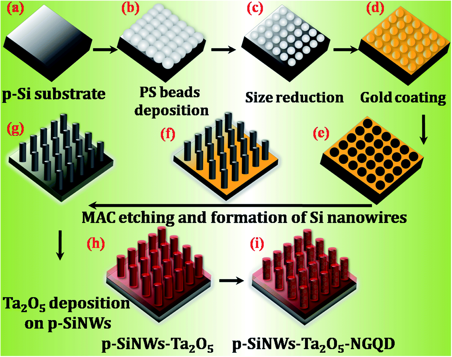 | ||
| Fig. 1 (a–g) Schematic of the fabrication of vertically aligned p-SiNWs using Metal-Assisted Chemical Etching (MACE). (h) Deposition of Ta2O5 by PLD. (i) The decoration of NGQD on the p-SiNWs–Ta2O5 matrix and the formation of the p-SiNWs–Ta2O5–NGQD heterostructure. | ||
The morphological and structural analysis of each step during the growth of the p-SiNWs–Ta2O5–NGQD heterostructure was probed by FE-SEM analysis and shown in Fig. 2. Fig. 2a shows the surface morphology of the as-dispersed PS beads, which confirms the presence of hexagonally oriented monolayer beads with a close packing geometry on the Si surface having a diameter of ∼450 nm (the inset shows a zoomed-in view). The as-dispersed monolayer of the PS beads was then etched with an optimized power of O2 plasma to reduce the diameter from 450 nm to ∼230 nm, thereby creating a uniform gap between the PS beads as shown in Fig. 2b. After the size reduction, the sample was uniformly coated with a thin layer of ∼30 nm gold (Au), followed by the formation of a gold mesh-like architecture (Fig. S1a†) created by the dissolution of PS beads in toluene solvent. The Au mesh catalyzed the oxidation process of the Si underneath by converting it into SiO2 in the presence of the oxidizing agent H2O2. HF solution was then used to dissolve the SiO2, resulting in the formation of uniformly dispersed vertically aligned SiNWs on the Si substrate. Thereafter, the Au was removed by aqua regia treatment to get rid of any metal contamination from the Si nanowire matrix. Fig. 2c shows the top view of the as-fabricated Si nanowires having diameters in the range of ∼220–225 nm and the average gap between the nanowires was ∼100–170 nm; the corresponding high magnification image is shown in the inset. Here, the etching duration was optimized to get the nanowires with diameter and length below the desired range of ∼250 nm and 1.5 μm, respectively, which provided efficient light trapping and low exciton diffusion length for enhanced PEC-HER performance.14,39 Subsequently, the as-grown p-SiNWs were coated with ∼40 nm Ta2O5 layer and the corresponding tilted image of the homogeneously patterned vertically aligned p-SiNWs–Ta2O5 arrays with an average length of ∼1.2 μm and diameter of ∼260 nm were observed as shown in Fig. 2d. Moreover, the thickness of the Ta2O5 film was optimized to maintain a conformal coating of the Si nanowires, avoiding any direct connection between the nanowires. Thus, the Ta2O5 layers with varying thicknesses of 15, 40, and 80 nm were grown and the respective FE-SEM images are shown in Fig. S1.† For the 15 nm coating (Fig. S1b†), only the top faces of the SiNWs were covered while the lower portions of the nanowires were left bare, which made them prone to oxidation under electrochemical analysis. On the other hand, 80 nm coating (Fig. S1d†) resulted in the blockage of gaps between the nanowires, resulting in the deterioration of effective light trapping, low catalyst loading and less accessibility of the electrolyte to the electrode surface. However, the optimized 40 nm coating of the Ta2O5 layer clearly represents a uniform decoration of Si nanowires with Ta2O5 while maintaining the equidistant gap between the nanowires, which is highly desired for the PEC-HER performance as shown in Fig. 2d and S1c.†
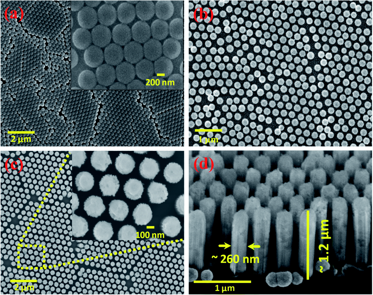 | ||
| Fig. 2 FE-SEM images of (a) the as-deposited monolayer of PS nano-beads (∼diameter 450 nm) on the silicon surface (inset shows the respective high-magnification image); (b) size reduction to ∼230 nm using O2 plasma etching; (c) top view of the as-prepared p-SiNWs; the inset shows a high-magnification image after MACE; (d) tilted view of the homogeneously patterned and vertically aligned p-SiNWs–Ta2O5 arrays where the diameter and height of the SiNWs were ∼260 nm and 1.2 μm, respectively. | ||
To characterize the as-prepared NGQD, various techniques like UV-Vis absorption, photoluminescence, FTIR, and Raman spectroscopy have been adopted. The as-prepared solutions of GQD and NGQD showed the transparent and faint yellow colour under sunlight (inset of Fig. S2a† and 3a); however, upon irradiation with a UV lamp, both showed blue photoluminescence with a brighter emission from NGQD (inset of Fig. S2b† and 3b). The UV-Vis spectra of GQD (Fig. S2a†) confirmed the formation of the C![[double bond, length as m-dash]](https://www.rsc.org/images/entities/char_e001.gif) O bond by showing a prominent absorption peak at 362 nm corresponding to the n–π* transition, which is in agreement with the previous report.38 In general, NGQD shows two characteristic peaks, one is at ∼230 nm, corresponding to the π–π* transition of the CC bond, and another at ∼340 nm, which is attributed to the n–π transition in the CO bond, (Fig. 3a).38,40 Upon excitation with a 370 nm beam, the PL spectrum of GQD showed a prominent peak at 461 nm with a Stokes shift of 91 nm (Fig. S2b†).38 However, the PL spectrum of the as-prepared NGQD, showed a strong peak at 423 nm for an excitation wavelength of 340 nm, confirming a Stoke's shift of 83 nm (Fig. 3b).38 This blue shift of the NGQD emission spectrum upon irradiation under a UV lamp is attributed to the relatively strong electron affinity of N-functionalities in NGQD, which further confirmed the formation of NGQD from GQD.38 The N-functionalities present in the NGQD were examined by the ATR-FTIR absorption spectrum, where bands at 3260–3132, 1625 cm−1, and 1452, 1150 cm−1 correspond to the formation of N–H, CN, and C–N bonds, respectively, as shown in Fig. S3.†38 Moreover, the Raman spectrum of the as-grown NGQD, shown in Fig. S4,† represents the peaks centered at ∼1365 and 1600 cm−1 corresponding to the D and G bands, which are attributed to the in-plane A1g and E2g mode of vibrations, respectively.41–43 Thus, the ratio of ID/IG (∼1.1), as well as the broadening of the D band in NGQD may be attributed to the incorporation of defect densities, the appearance of surface functional groups and/or the presence of non-carbonaceous elements in the graphitic matrix.44 The broadening of the D band as compared to the G band is a further authentication of the intercalation of nitrogen atoms into the base carbon backbone creating disordered structures.42 The diameter of the as-grown NGQD was found to be in the range of 3–4 nm as measured in AFM analysis (Fig. S5†). The tiny NGQD particles uniformly decorated on the nanowire surface act as a catalyst in the photoelectrochemical process, as discussed in a later section. Further elucidation of the hybrid nanowire architecture and its crystallinity was achieved via in-depth TEM analysis.
O bond by showing a prominent absorption peak at 362 nm corresponding to the n–π* transition, which is in agreement with the previous report.38 In general, NGQD shows two characteristic peaks, one is at ∼230 nm, corresponding to the π–π* transition of the CC bond, and another at ∼340 nm, which is attributed to the n–π transition in the CO bond, (Fig. 3a).38,40 Upon excitation with a 370 nm beam, the PL spectrum of GQD showed a prominent peak at 461 nm with a Stokes shift of 91 nm (Fig. S2b†).38 However, the PL spectrum of the as-prepared NGQD, showed a strong peak at 423 nm for an excitation wavelength of 340 nm, confirming a Stoke's shift of 83 nm (Fig. 3b).38 This blue shift of the NGQD emission spectrum upon irradiation under a UV lamp is attributed to the relatively strong electron affinity of N-functionalities in NGQD, which further confirmed the formation of NGQD from GQD.38 The N-functionalities present in the NGQD were examined by the ATR-FTIR absorption spectrum, where bands at 3260–3132, 1625 cm−1, and 1452, 1150 cm−1 correspond to the formation of N–H, CN, and C–N bonds, respectively, as shown in Fig. S3.†38 Moreover, the Raman spectrum of the as-grown NGQD, shown in Fig. S4,† represents the peaks centered at ∼1365 and 1600 cm−1 corresponding to the D and G bands, which are attributed to the in-plane A1g and E2g mode of vibrations, respectively.41–43 Thus, the ratio of ID/IG (∼1.1), as well as the broadening of the D band in NGQD may be attributed to the incorporation of defect densities, the appearance of surface functional groups and/or the presence of non-carbonaceous elements in the graphitic matrix.44 The broadening of the D band as compared to the G band is a further authentication of the intercalation of nitrogen atoms into the base carbon backbone creating disordered structures.42 The diameter of the as-grown NGQD was found to be in the range of 3–4 nm as measured in AFM analysis (Fig. S5†). The tiny NGQD particles uniformly decorated on the nanowire surface act as a catalyst in the photoelectrochemical process, as discussed in a later section. Further elucidation of the hybrid nanowire architecture and its crystallinity was achieved via in-depth TEM analysis.
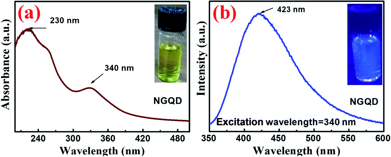 | ||
| Fig. 3 (a) Absorbance spectra and the inset shows the solution colour under sunlight. (b) PL spectra of NGQD at an excitation wavelength of 340 nm and the inset shows the solution colour under UV irradiation. | ||
Fig. 4a shows the cross-sectional schematic of the designed p-SiNWs–Ta2O5–NGQD heterostructure where the Si nanowires having diameters in the range of ∼220 nm are uniformly decorated with 40 nm thick Ta2O5 (Fig. 4b and its corresponding inset). This analysis corroborates the previously observed macroscopic FE-SEM characterization (Fig. 2d). The high-resolution TEM (HR-TEM) analysis indicated the lattice fringes corresponding to Si nanowires in the (100) direction, confirming the vertically oriented growth and uniform coating with the Ta2O5 thin film.16 The corresponding d-spacing of ∼0.30 nm is responsible for the Si (100) plane, whereas the d-spacing of ∼0.23 nm refers to the formation of the Ta2O5 (111) plane corresponding to orthorhombic facets and confirms the decoration of the heterostructure interface as shown in Fig. 4c.16,45,46 The selected area electron diffraction (SAED) pattern shows the planes corresponding to both Si and Ta2O5 and validates that the formation of the Si–Ta2O5 heterojunction is polycrystalline in nature as shown in Fig. 4d. From the SAED pattern, the corresponding lattice spacings have been calculated and are tabulated in Table S1.† However, the presence of all lattice fringes corresponding to SiNWs, Ta2O5, and NGQD in a single frame of HR-TEM analysis is hard to detect because the lattice fringes of NGQD (100) and Ta2O5 (111) fall in a nearly similar range of ∼0.21 nm and ∼0.23 nm, respectively.16,47 Similarly, the lattice fringes of NGQD (002) and Si (100) also fall in the identical range of ∼0.34 nm and ∼0.30 nm, respectively.16,47,48 Thus, Si (100) and NGQD (002) lattice fringes have been separately identified in a single platform (Fig. S6†) which indicates the presence of three-sub lattices in the designed heterostructure. The formation of Ta2O5 can also be verified by XRD analysis (Fig. S7†) where the peaks at 23.81 29.16, 36.52, and 55.52° correspond to the lattice plans of (001), (200), (201) and (1112), respectively, which come from the crystalline facets of Ta2O5 and the peak at 33.09° is responsible for the plane of Si (100).49–52 The surface impregnation of NGQD decorated on top of p-SiNWs–Ta2O5 was probed by the XPS survey scan of the as-synthesized p-SiNWs–Ta2O5–NGQD photocathodes (Fig. S8†) where the presence of all the elements (Si, Ta, O, N, C) confirmed the formation of the desired heterostructure.53–56 The deconvoluted high-resolution peaks of Si 2s and Si 2p at the binding energies of 151.18 and 100.36 eV reveal the crystalline chemical state of the Si atom which is from the p-SiNWs (Fig. S9†).57,58 The uniform deposition of the Ta2O5 can be confirmed by the high-resolution spectra (Fig. S9†) of Ta 4d (230.25 eV) and O 1s (530.82 eV).59–61 The Ta 4f spectrum was also analyzed, and it was further split into Ta 4f7/2 (26.01 eV) and Ta 4f5/2 (27.86 eV) due to strong spin–orbital coupling revealing the crystalline phases of Ta2O5.59 The O 1s spectrum shows an additional peak at a slightly higher binding energy centered at 532.4 eV, indicating the presence of the –OH and –CO groups associated with the NGQD matrix.59 The C 1s spectrum (Fig. S9f†) of NGQD has a major peak centered at 284.48 eV, which revealed the presence of C atoms in the C–C bonds, whereas the formation of C–OH and N–CN in aromatic rings can be verified by the peak positions at 285.98 and 287.74 eV, respectively.12,38,62 A small peak at 289.95 eV represents plasmon excitations of the carbon atom.12 In the N 1s spectrum, the two primary peaks at 398.59 and 400.98 eV correspond to the pyridinic-N and graphitic-N functionalities in the NGQD matrix.12,38,62 The higher binding energy peak at 403.86 eV indicated the presence of oxidative N–O(–C) species that may be responsible for creating the trap layer during the electron transfer process.12
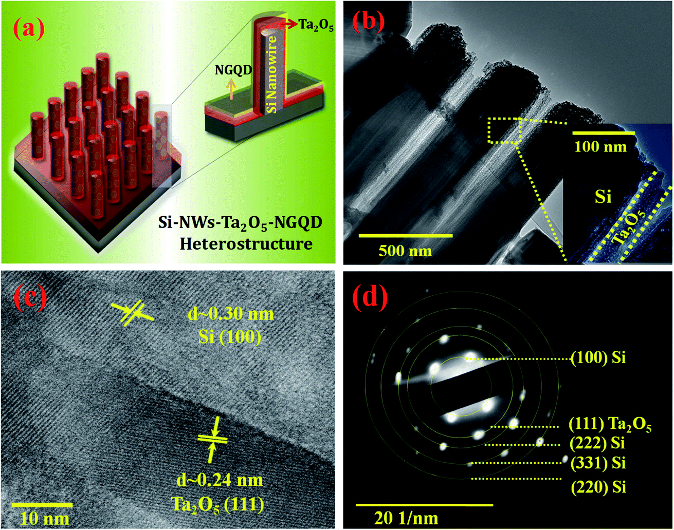 | ||
| Fig. 4 (a) Cross-sectional schematic of the designed p-SiNWs–Ta2O5–NGQD heterostructure. (b) TEM image of p-SiNWs decorated with a Ta2O5 layer on its surface, the inset reveals the zoomed-in view of the interface. (c) HR-TEM image depicting the interface of p-SiNWs (d ∼ 0.30 nm of silicon (100) planes) and Ta2O5 (d ∼ 0.24 nm corresponding to the (111) in-plane lattice spacing) depicting the lattice fringes of Si and Ta2O5, respectively. (d) Selective area electron diffraction (SAED) pattern confirming the planes corresponding to both Si and Ta2O5, validating the presence of the Si–Ta2O5 heterojunction. | ||
The electrochemical performance was analyzed via linear sweep voltammetry (LSV) measurements in a conventional three-electrode set-up connected to a potentiostat in 1 M HClO4 solution. The as-prepared p-SiNWs, p-SiNWs–NGQD, and p-SiNWs–Ta2O5–NGQD photocathodes have been tested under both dark and illuminated (100 mW cm−2) conditions as shown in Fig. S10† and 5, respectively. A rapid increase in the photocurrent density (Jph) was observed for p-SiNWs–NGQD as compared to bare p-SiNWs and finally reached a maximum value of −49.5 mA cm−2 at −0.78 V (vs. RHE) for the p-SiNWs–Ta2O5–NGQD photocathode as evidenced from Fig. 5a. The Jph value of p-SiNWs–NGQD was found to be −8.5 mA cm−2, which was ∼6 times lower as compared to the p-SiNWs–Ta2O5–NGQD photocathode at an applied potential of −0.78 V (vs. RHE). Moreover, it has been observed that under dark conditions, the current density (Jdark) value was reduced to almost one-fifth and was measured to be −10.05 mA cm−2 for the p-SiNWs–Ta2O5–NGQD photocathode. To investigate the photoelectrochemical effect of p-SiNWs–Ta2O5–NGQD with the variation of the thickness of Ta2O5 as a passivation layer, three different samples with Ta2O5 thicknesses of 15 nm, 40 nm, and 80 nm along with NGQD coating were prepared and the respective LSV plots are shown in Fig. S11.† It is evident from the LSV plots that the photocathode having the 40 nm Ta2O5 passivation layer provided the maximum photocurrent density as compared to all other thicknesses. This is attributed to the uniform decoration of the Si nanowires by the 40 nm Ta2O5 layer, which provided a conformal coating and enabled efficient charge separation and transfer throughout the nanowire length, as well as the accessibility of the electrolyte to the effectively exposed nanowire surface. In contrast, a 15 nm coating of Ta2O5 was deposited only at the top portion of the SiNWs, however, 80 nm deposition entirely blocked the gaps between the nanowires and thereby hindered the uniform catalyst loading throughout the nanowire surface and the facile accessibility of the electrolyte, which in turn led to low photocurrent density as shown in Fig. S11.† The optimized p-SiNWs–Ta2O5–NGQD photocathode performance towards the PEC-HER was investigated in terms of low overpotentials of −449 mV @ 5 mA cm−2 and −498 mV @ 10 mA cm−2, as compared to all other prepared electrodes, which indicates the compatibility of Ta2O5 with Si as an effective electron transport layer along with NGQD, as shown in Table S2.† The significant enhancement of Jph as compared to Jdark and the low value of the overpotential proved the superiority of Ta2O5, which not only behaves as a protective layer but also acts as a smooth charge transport matrix because of negligible lattice mismatch with Si.27
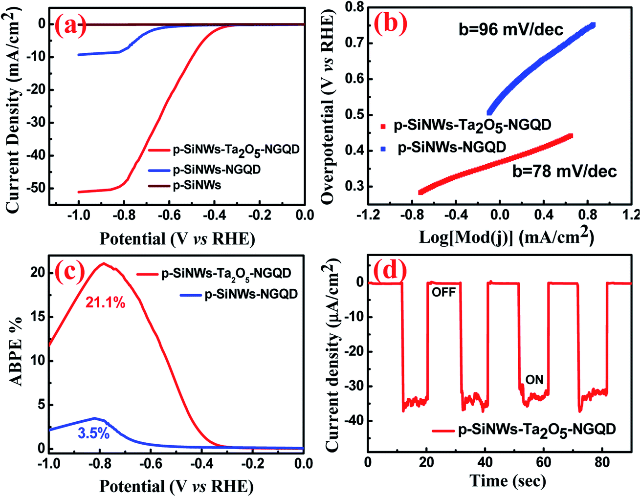 | ||
| Fig. 5 (a) LSV polarization curve (without iR correction) for p-SiNWs, p-SiNWs–NGQD, and p-SiNWs–Ta2O5–NGQD in 1 M HClO4 solution under illumination. (b) Tafel plot of the p-SiNWs–Ta2O5–NGQD and p-SiNWs–NGQD heterostructure under illuminated conditions. (c) ABPE of p-SiNWs–Ta2O5–NGQD and p-SiNWs–NGQD heterostructures. (d) Transient photo-response of the p-SiNWs–Ta2O5–NGQD heterostructure under repeated ON/OFF cycles at an interval of 10 seconds. | ||
For an in-depth analysis of the catalytic activity and the HER reaction kinetics of p-SiNWs–Ta2O5–NGQD and the p-SiNWs–NGQD photoelectrode, the corresponding Tafel slopes were calculated using the Tafel equation under illuminated conditions, as shown in Fig. 5b. The relatively low value of the Tafel slope of 78 mV dec−1 for the p-SiNWs–Ta2O5–NGQD photoelectrode as compared to p-SiNWs–NGQD (96 mV dec−1) indicates a faster electron transfer via the Volmer–Heyrovsky mechanism where the electrochemical desorption following the Heyrovsky pathway is referred to as the rate-limiting step for HER kinetics.32,63 The detailed mechanism has been discussed in the ESI.† Moreover, the exchange current density was calculated (Fig. S12†) via extrapolating the Tafel plots to the X-axis12 and its larger value of 118 μA cm−2 for p-SiNWs–Ta2O5–NGQD as compared to p-SiNWs–NGQD photocathode (53 μA cm−2), indicates a faster electron transfer process at the electrode/electrolyte interface with a low kinetic barrier. The electrochemical impedance spectroscopy (EIS) measurements were carried out for the p-SiNWs–Ta2O5–NGQD photocathode under both illuminated and dark conditions at an applied voltage of −300 mV (vs. RHE) and the corresponding Nyquist plots have been analyzed (Fig. S13†). The charge transfer resistance (Rct) value under illumination was found to be 306 ohms, which is nearly half of that of the dark condition (663 ohm). This significant reduction in Rct at the photocathode/electrolyte interface under illuminated conditions confirmed the role of Ta2O5–NGQD decoration on SiNWs as an effective moderator to hasten the charge transfer kinetics via a low barrier interface and the corresponding equivalent circuit diagram has been incorporated as the inset of Fig. S13.† The low value of Rct under illuminated conditions is attributed to the enhanced photoexcited carrier generation, and the faster and smoother electron transfer process. The applied bias photon-to-current conversion efficiency (ABPE) was calculated using the following equation:11,12,16
| ABPE = [Jph × (Vreverse − Vapplied)/Pin] × 100% |
The applicability of the as-designed catalyst for prolonged hydrogen generation was verified under chronopotentiometric measurement (Fig. 6a) in 1 M HClO4 solution for at least 10 hours at an applied current density of 10 mA cm−2 and showed a minimum potential loss of ∼5%, indicating a moderately stable p-SiNWs–Ta2O5–NGQD photocathode. The stability of the photocathode may be attributed to the uniform coating of the protective Ta2O5 layer, followed by its decoration with the non-corrosive carbonaceous matrix, which diminished the chance of Si surface oxidation under operational conditions. The cyclic stability test was performed under repeated LSV at a 5 mV s−1 scan rate (Fig. 6b) and there was high cycling stability of the robust photocathode with a minimum decrease of overpotential of 3% @ −20 mA cm−2 after 1000 cycles.
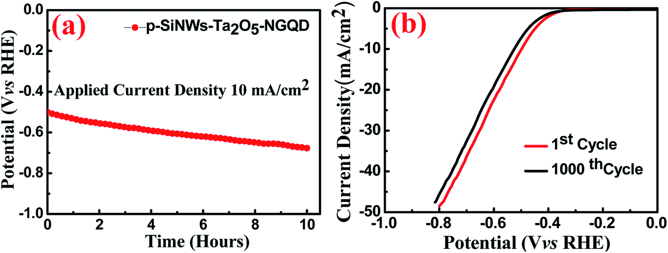 | ||
| Fig. 6 (a) Chronopotentiometry measurement of p-SiNWs–Ta2O5–NGQD at an applied current density of 10 mA cm−2 under illumination. (b) LSV polarization curve of the 1st and 1000th cycle at 5 mV S−1 under a rigorous cycling process. | ||
The extent of band-bending for the overall PEC performance of the Ta2O5–NGQD-modified SiNWs was compared with p-SiNWs–NGQD, p-SiNWs–Ta2O5, and bare SiNWs under capacitance measurements, followed by the corresponding Mott–Schottky (M–S) plots, as shown in Fig. 7a and S15,† respectively. In semiconductor electrochemistry, the M–S plot describes the capacitance value versus the potential difference between the semiconductor and the electrolyte.65 Therefore, from the M–S plot, the qualitative analysis of the conductivity types and the carrier concentration of semiconductors can be obtained. The p-type conductivity of the Si wafer was confirmed from the negative slope of the M–S plot66 as shown in Fig. S15a.† However, coating with Ta2O5 and/or NGQD imparted the positive slope, indicating the n-type character. Different parameters like flat-band potential, carrier concentration, and barrier height have been calculated from the M–S plot (Table S4†) and the detailed calculation methods67 have been described in the ESI.† The flat band potential (Efb) of p-SiNWs–Ta2O5–NGQD was found to be −0.78 V, while that of p-SiNWs–Ta2O5, p-SiNWs–NGQD and p-SiNWs were calculated to be −0.29 V, 0.12 V, and 0.07 V, respectively. The higher value of Efb in the case of p-SiNWs–Ta2O5–NGQD augments the extent of higher band bending at the depletion region of the heterostructure and thereby signifies faster excitonic charge separation and simultaneously suppresses recombination at the electrode–electrolyte interface, leading to significantly enhanced photo-current density.65,67 For the p-SiNWs–Ta2O5–NGQD photocathode, Ta2O5 plays a crucial role due to its low lattice mismatch, less trap-state generation, and low conduction band offset, enabling a faster electron transfer process and thereby suppressing carrier recombination. In addition, the carrier concentrations were calculated from the slope of the M–S plot and were found to be 4.19 × 1017 cm−3 and 6.67 × 1016 cm−3 for p-SiNWs–Ta2O5–NGQD and p-SiNWs–NGQD, respectively, which can be attributed to the enhancement of the carrier generation upon the introduction of the Ta2O5 passivation layer. The barrier heights of the p-SiNWs–NGQD matrix with and without metal oxide (Ta2O5) were found to be 0.67 and 0.22 V, respectively. Such a large barrier height for p-SiNWs–Ta2O5–NGQD can be attributed to the generation of a strong inversion layer at the Si surface owing to the increased band bending and consequently, it enhanced the charge-carrier generation and separation within the semiconductor heterostructure. Thus, the Ta2O5 layer allows electron transfer (very small lattice mismatch and low conduction band offset) and prevents hole transfer (high valence band offset) from Si, which makes it an effective passivation material for the dangling ends of Si, promoting higher band-bending and large photocurrent density, thus endorsing improved PEC performance. The overall mechanism can be understood by the bi-functional role of Ta2O5–NGQD, which not only enhances the absorption but also plays a crucial role as an active passivation layer (Ta2O5) and catalyst (NGQD). Since the band alignment of Ta2O5 lies in a similar range of water redox potential, it helps in transferring hot electrons, thereby facilitating the directional superior electron transfer from Si to the electrolyte assisted by the energy levels of Ta2O5–NGQD. Further, the charge transport mechanism is explained with the help of the schematic energy band diagram as portrayed in Fig. 7b. The band edge positions of Ta2O5 and NGQD have been schematically illustrated as sourced from the literature reports.27,30,68 Upon both solar irradiation and applied potential, the majority of the photo-generated electrons moved from Si to the NGQD via the Ta2O5 passivation layer, whereas holes (h+) returned from NGQD to Si.
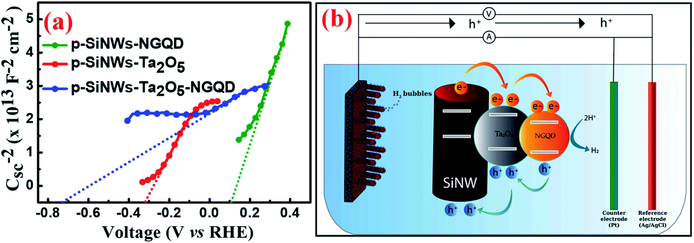 | ||
| Fig. 7 (a) Mott–Schottky analysis of p-SiNWs–Ta2O5–NGQD, p-SiNWs–NGQD, and p-SiNWs–Ta2O5 photocathodes. (b) A schematic illustration of the charge transfer mechanism of the p-SiNWs–Ta2O5–NGQD photocatalyst in the PEC-HER. | ||
In summary, the outstanding performance of the as-designed p-SiNWs–Ta2O5–NGQD heterostructure can be attributed to the following: (1) as compared to planar Si, the nano-texturing of Si (i.e. SiNWs) facilitates superior light absorption through multiple scattering and enhancing photo-generated carriers. (2) The high surface-to-volume ratio of the one-dimensional Si nanowire arrays provides a high surface area for catalyst loading. (3) The introduction of Ta2O5 as a passivation layer with a negligible lattice mismatch provides a less resistive path via reducing the defects at the interface. (4) The excellent passivation, inhibition of the recombination of e− and h+ under light irradiation, and facile electron transfer via Ta2O5 promote higher band-bending and large photocurrent density, which enhance the overall performance of the p-SiNWs–Ta2O5–NGQD electrode. (5) The incorporation of the metal-free catalyst NGQD enables absorption in the UV region, reduces the possibility of surface poisoning, and it is known to have sharp catalytic edges and high charge mobility. (6) Additionally, NGQD facilitates a low resistance path for electron transfer towards the electrolyte and also accelerates the photo-electrochemical HER kinetics on its surface. (7) The uniform coating of the Si surface with Ta2O5 and its decoration with NGQD contribute to the moderate catalytic stability, which may be attributed to the negligible chance of surface oxidation as well as the non-corrosive nature of NGQD under an acidic medium. In this context, the as-grown p-SiNWs–Ta2O5–NGQD heterostructure creates a new avenue for delivering low-cost, stable, highly efficient silicon-based PEC-HER technology.
Conclusion
The present report demonstrates the design of vertically aligned p-SiNWs uniformly coated with Ta2O5 and finally decorated with a uniform metal-free (NGQD) catalyst as an efficient photocathode for the photoelectrochemical HER. The superiority of the as-designed p-SiNWs–Ta2O5–NGQD heterostructure towards the PEC-HER has been examined in terms of its high photocurrent density of −49.5 mA cm−2 and ABPE of ∼21.1% at a potential of −0.78 V (vs. RHE). Moreover, the lower values of the Tafel slope (78 mV dec−1) and overpotential (−498 mV @ 10 mA cm−2) add to its effectiveness towards HER kinetics. This remarkably improved photo electrocatalytic performance is attributed to the optimal band alignment of the heterostructure, owing to the sequential decoration of Ta2O5 and NGQD on the silicon nanowire surface facilitating the broadband absorption and faster excitonic separation and transportation. The cost-effective and environment-friendly approach, compatible with the ongoing Si-based technology, unveils the innovation towards the development of renewable hydrogen fuel for industry-grade applications.Author contributions
S. R. did all the electrochemical study, characterization, data analysis and manuscript writing/revision, J. S. was involved in manuscript writing and data analysis, S. A. S. and D. B. were associated with the fabrication and characterization of as prepared materials, S. K. and D. B. were involved in Mott–Schottky analysis, S. S. Y. and A. V. helped to perform plasma etching of PS beads and SEM characterization, S. G. and S. C. were involved in deposition of Ta2O5 using PLD system, K. G. was associated with writing, revision and overall supervision of the work.Conflicts of interest
There are no conflicts to declare.Acknowledgements
For the successful execution of this work, K. G. is thankful to Nanomission (Grant No-SR-/NM/NS-91/2016), Department of Science and Technology, Govt. of India for financial support and Institute of Nano Science and Technology, Mohali, India for the research facility.References
- Y. Hou, E. Aydin, M. De Bastiani, C. Xiao, F. H. Isikgor, D.-J. Xue, B. Chen, H. Chen, B. Bahrami, A. H. Chowdhury, A. Johnston, S.-W. Baek, Z. Huang, M. Wei, Y. Dong, J. Troughton, R. Jalmood, A. J. Mirabelli, T. G. Allen, E. Van Kerschaver, M. I. Saidaminov, D. Baran, Q. Qiao, K. Zhu, S. De Wolf and E. H. Sargent, Science, 2020, 367, 1135–1140 CrossRef CAS PubMed.
- A. Kudo and Y. Miseki, Chem. Soc. Rev., 2009, 38, 253–278 RSC.
- S. Chu and A. Majumdar, Nature, 2012, 488, 294–303 CrossRef CAS PubMed.
- N. S. Lewis and D. G. Nocera, Proc. Natl. Acad. Sci., 2006, 103, 15729–15735 CrossRef CAS PubMed.
- A. Angelis-Dimakis, M. Biberacher, J. Dominguez, G. Fiorese, S. Gadocha, E. Gnansounou, G. Guariso, A. Kartalidis, L. Panichelli, I. Pinedo and M. Robba, Renewable Sustainable Energy Rev., 2011, 15, 1182–1200 CrossRef.
- M. Grätzel, Nature, 2001, 414, 338–344 CrossRef PubMed.
- O. Khaselev, Science, 1998, 280, 425–427 CrossRef CAS PubMed.
- A. J. Bard and M. A. Fox, Acc. Chem. Res., 1995, 28, 141–145 CrossRef CAS.
- C. Tang, R. Zhang, W. Lu, Z. Wang, D. Liu, S. Hao, G. Du, A. M. Asiri and X. Sun, Angew. Chem., 2017, 129, 860–864 CrossRef.
- Y. Lin, C. Battaglia, M. Boccard, M. Hettick, Z. Yu, C. Ballif, J. W. Ager and A. Javey, Nano Lett., 2013, 13, 5615–5618 CrossRef CAS PubMed.
- D. Ghosh, K. Roy, K. Sarkar, P. Devi and P. Kumar, ACS Appl. Mater. Interfaces, 2020, 12, 28792–28800 CrossRef CAS PubMed.
- S. Riyajuddin, S. Kumar, D. Badhwar, S. A. Siddiqui, J. Sultana and K. Ghosh, Sustainable Energy Fuels, 2021, 5(12), 3160–3171 RSC.
- Y. Yang, M. Wang, P. Zhang, W. Wang, H. Han and L. Sun, ACS Appl. Mater. Interfaces, 2016, 8, 30143–30151 CrossRef CAS PubMed.
- S. Huang, H. Zhang, Z. Wu, D. Kong, D. Lin, Y. Fan, X. Yang, Z. Zhong, S. Huang, Z. Jiang and C. Cheng, ACS Appl. Mater. Interfaces, 2014, 6, 12111–12118 CrossRef CAS PubMed.
- I. Oh, J. Kye and S. Hwang, Nano Lett., 2012, 12, 298–302 CrossRef CAS PubMed.
- K. Roy, D. Ghosh, K. Sarkar, P. Devi and P. Kumar, ACS Appl. Mater. Interfaces, 2020, 12, 37218–37226 CrossRef CAS PubMed.
- B. Weng, F. Xu and J. Xu, Nanotechnology, 2014, 25, 455402 CrossRef PubMed.
- P. D. Tran, S. S. Pramana, V. S. Kale, M. Nguyen, S. Y. Chiam, S. K. Batabyal, L. H. Wong, J. Barber and J. Loo, Chem.–Eur. J., 2012, 18, 13994–13999 CrossRef CAS PubMed.
- C. Lv, Z. Chen, Z. Chen, B. Zhang, Y. Qin, Z. Huang and C. Zhang, J. Mater. Chem. A, 2015, 3, 17669–17675 RSC.
- D. Zhang, J. Shi, W. Zi, P. Wang and S. Liu, ChemSusChem, 2017, 10, 4324–4341 CrossRef CAS PubMed.
- L. Ji, M. D. McDaniel, S. Wang, A. B. Posadas, X. Li, H. Huang, J. C. Lee, A. A. Demkov, A. J. Bard, J. G. Ekerdt and E. T. Yu, Nat. Nanotechnol., 2015, 10, 84–90 CrossRef CAS PubMed.
- D. V. Esposito, I. Levin, T. P. Moffat and A. A. Talin, Nat. Mater., 2013, 12, 562–568 CrossRef CAS PubMed.
- S. M. Thalluri, L. Bai, C. Lv, Z. Huang, X. Hu and L. Liu, Adv. Sci., 2020, 7, 1902102 CrossRef CAS PubMed.
- Y. Wan, S. K. Karuturi, C. Samundsett, J. Bullock, M. Hettick, D. Yan, J. Peng, P. R. Narangari, S. Mokkapati, H. H. Tan, C. Jagadish, A. Javey and A. Cuevas, ACS Energy Lett., 2018, 3, 125–131 CrossRef CAS.
- C. Battaglia, S. M. de Nicolás, S. De Wolf, X. Yin, M. Zheng, C. Ballif and A. Javey, Appl. Phys. Lett., 2014, 104, 113902 CrossRef.
- S. Avasthi, W. E. McClain, G. Man, A. Kahn, J. Schwartz and J. C. Sturm, Appl. Phys. Lett., 2013, 102, 203901 CrossRef.
- T. Wang, S. Liu, H. Li, C. Li, Z. Luo and J. Gong, Ind. Eng. Chem. Res., 2019, 58, 5510–5515 CrossRef CAS.
- R. Ghosh and P. K. Giri, Nanotechnology, 2016, 28, 012001 CrossRef PubMed.
- Y. Sim, J. John, J. Moon and U. Sim, Appl. Sci., 2018, 8, 2046 CrossRef CAS.
- U. Sim, J. Moon, J. Lee, J. An, H.-Y. Ahn, D. J. Kim, I. Jo, C. Jeon, S. Han, B. H. Hong and K. T. Nam, ACS Appl. Mater. Interfaces, 2017, 9, 3570–3580 CrossRef CAS PubMed.
- U. Sim, T.-Y. Yang, J. Moon, J. An, J. Hwang, J.-H. Seo, J. Lee, K. Y. Kim, J. Lee, S. Han, B. H. Hong and K. T. Nam, Energy Environ. Sci., 2013, 6, 3658–3664 RSC.
- U. Sim, J. Moon, J. An, J. H. Kang, S. E. Jerng, J. Moon, S.-P. Cho, B. H. Hong and K. T. Nam, Energy Environ. Sci., 2015, 8, 1329–1338 RSC.
- N. Ou, H. Li, B. Lyu, B. Gui, X. Sun, D. Qian, Y. Jia, X. Wang and J. Yang, Catalysts, 2019, 9, 345 CrossRef.
- S. Riyajuddin, S. K. T. Aziz, S. Kumar, G. D. Nessim and K. Ghosh, ChemCatChem, 2020, 12, 1394–1402 CrossRef CAS.
- X.-Q. Bao, D. Y. Petrovykh, P. Alpuim, D. G. Stroppa, N. Guldris, H. Fonseca, M. Costa, J. Gaspar, C. Jin and L. Liu, Nano Energy, 2015, 16, 130–142 CrossRef CAS.
- S. M. Thalluri, J. Borme, K. Yu, J. Xu, I. Amorim, J. Gaspar, L. Qiao, P. Ferreira, P. Alpuim and L. Liu, Nano Res., 2018, 11, 4823–4835 CrossRef CAS.
- Z. Huang, N. Geyer, P. Werner, J. de Boor and U. Gösele, Adv. Mater., 2011, 23, 285–308 CrossRef CAS PubMed.
- Y.-N. Hao, H.-L. Guo, L. Tian and X. Kang, RSC Adv., 2015, 5, 43750–43755 RSC.
- S. M. Thalluri, J. Borme, D. Xiong, J. Xu, W. Li, I. Amorim, P. Alpuim, J. Gaspar, H. Fonseca, L. Qiao and L. Liu, Sustainable Energy Fuels, 2018, 2, 978–982 RSC.
- D. Qu, M. Zheng, L. Zhang, H. Zhao, Z. Xie, X. Jing, R. E. Haddad, H. Fan and Z. Sun, Sci. Rep., 2014, 4, 5294 CrossRef CAS PubMed.
- N.-J. Kuo, Y.-S. Chen, C.-W. Wu, C.-Y. Huang, Y.-H. Chan and I.-W. P. Chen, Sci. Rep., 2016, 6, 30426 CrossRef CAS PubMed.
- Y. Li, Y. Zhao, H. Cheng, Y. Hu, G. Shi, L. Dai and L. Qu, J. Am. Chem. Soc., 2012, 134, 15–18 CrossRef CAS PubMed.
- S. Riyajuddin, S. Kumar, K. Soni, S. P. Gaur, D. Badhwar and K. Ghosh, Nanotechnology, 2019, 30, 385702 CrossRef CAS PubMed.
- S. Riyajuddin, S. Kumar, S. P. Gaur, A. Sud, T. Maruyama, M. E. Ali and K. Ghosh, Nanotechnology, 2020, 31, 295501 CrossRef CAS PubMed.
- K. N. Manukumar, B. Kishore, R. Viswanatha and G. Nagaraju, J. Solid State Electrochem., 2020, 24, 1067–1074 CrossRef CAS.
- G. Nagaraju, K. Karthik and M. Shashank, Microchem. J., 2019, 147, 749–754 CrossRef CAS.
- Y. Dong, H. Pang, H. B. Yang, C. Guo, J. Shao, Y. Chi, C. M. Li and T. Yu, Angew. Chem., Int. Ed., 2013, 52, 7800–7804 CrossRef CAS PubMed.
- B. Zheng, Y. Chen, P. Li, Z. Wang, B. Cao, F. Qi, J. Liu, Z. Qiu and W. Zhang, Nanophotonics, 2017, 6, 259–267 CAS.
- Y. C. Lam, H. Y. Zheng, R. T. Tjeung and X. Chen, J. Phys. D: Appl. Phys., 2009, 42, 042004 CrossRef.
- K. Miura, T. Osawa, Y. Yokota, T. Suzuki and O. Hanaizumi, Results Phys., 2014, 4, 148–149 CrossRef.
- S. Zhou, Z. Deng, Z. Wu, M. Xie, Y. Tian, Y. Wu, J. Liu, G. Li and Q. He, Nanomaterials, 2019, 9, 811 CrossRef CAS PubMed.
- R. R. Krishnan, K. G. Gopchandran, V. P. MahadevanPillai, V. Ganesan and V. Sathe, Appl. Surf. Sci., 2009, 255, 7126–7135 CrossRef CAS.
- L. F. Edge, D. G. Schlom, R. T. Brewer, Y. J. Chabal, J. R. Williams, S. A. Chambers, C. Hinkle, G. Lucovsky, Y. Yang, S. Stemmer, M. Copel, B. Holländer and J. Schubert, Appl. Phys. Lett., 2004, 84, 4629–4631 CrossRef CAS.
- R. Bywalez, H. Karacuban, H. Nienhaus, C. Schulz and H. Wiggers, Nanoscale Res. Lett., 2012, 7, 76 CrossRef PubMed.
- M. Hellwig, A. Milanov, D. Barreca, J.-L. Deborde, R. Thomas, M. Winter, U. Kunze, R. A. Fischer and A. Devi, Chem. Mater., 2007, 19, 6077–6087 CrossRef CAS.
- D. Y. Osadchii, A. I. Olivos-Suarez, A. V. Bavykina and J. Gascon, Langmuir, 2017, 33, 14278–14285 CrossRef CAS PubMed.
- C. Albonetti, J. Martinez, N. S. Losilla, P. Greco, M. Cavallini, F. Borgatti, M. Montecchi, L. Pasquali, R. Garcia and F. Biscarini, Nanotechnology, 2008, 19, 435303 CrossRef PubMed.
- S. C. Ray, D. K. Mishra, A. M. Strydom and P. Papakonstantinou, J. Appl. Phys., 2015, 118, 115302 CrossRef.
- K. Kosiel, K. Pągowska, M. Kozubal, M. Guziewicz, K. Lawniczak-Jablonska, R. Jakieła, Y. Syryanyy, T. Gabler and M. Śmietana, J. Vac. Sci. Technol., A, 2018, 36, 031505 CrossRef.
- R. V. Gonçalves, R. Wojcieszak, P. M. Uberman, S. R. Teixeira and L. M. Rossi, Phys. Chem. Chem. Phys., 2014, 16, 5755–5762 RSC.
- H. Cho, K. W. Park, J. H. Ahn, C. H. Park, H. J. Cho, S. J. Yeom, K. Hong and N. J. Kwak, ECS Trans., 2014, 61, 21 CrossRef CAS.
- L. Tang, R. Ji, X. Li, G. Bai, C. P. Liu, J. Hao, J. Lin, H. Jiang, K. S. Teng, Z. Yang and S. P. Lau, ACS Nano, 2014, 8, 6312–6320 CrossRef CAS PubMed.
- S. Riyajuddin, K. Azmi, M. Pahuja, S. Kumar, T. Maruyama, C. Bera and K. Ghosh, ACS Nano, 2021, 15, 5586–5599 CrossRef CAS PubMed.
- P. Perez-Rodriguez, D. Cardenas-Morcoso, I. A. Digdaya, A. M. Raventos, P. Procel, O. Isabella, S. Gimenez, M. Zeman, W. A. Smith and A. H. M. Smets, ChemSusChem, 2018, 11, 1797–1804 CrossRef CAS PubMed.
- B. Liu, S. Feng, L. Yang, C. Li, Z. Luo, T. Wang and J. Gong, Energy Environ. Sci., 2020, 13, 221–228 RSC.
- Z. Luo, T. Wang and J. Gong, Chem. Soc. Rev., 2019, 48, 2158–2181 RSC.
- I. A. Digdaya, G. W. P. Adhyaksa, B. J. Trześniewski, E. C. Garnett and W. A. Smith, Nat. Commun., 2017, 8, 15968 CrossRef CAS PubMed.
- W.-J. Chun, A. Ishikawa, H. Fujisawa, T. Takata, J. N. Kondo, M. Hara, M. Kawai, Y. Matsumoto and K. Domen, J. Phys. Chem. B, 2003, 107, 1798–1803 CrossRef CAS.
Footnote |
| † Electronic supplementary information (ESI) available. See DOI: 10.1039/d1se01280k |
| This journal is © The Royal Society of Chemistry 2022 |