
 Open Access Article
 This Open Access Article is licensed under a Creative Commons Attribution-Non Commercial 3.0 Unported Licence
Efficiency improvement for perovskite-inspired Cs3Sb2I9 solar cells using P3HT as the hole transport material†
Arto
Hiltunen‡
*,
Noora
Lamminen‡
,
Henri
Salonen
,
Maning
Liu
 and
Paola
Vivo
*
and
Paola
Vivo
*
Hybrid Solar Cells, Faculty of Engineering and Natural Sciences, Tampere University, P.O. Box 541, FI-33014 Tampere, Finland. E-mail: paola.vivo@tuni.fi
First published on 1st December 2021
Abstract
In this work, we introduce P3HT (poly(3-hexylthiophene-2,5-diyl)) as an efficient hole transport material (HTM) for lead-free Cs3Sb2I9 perovskite-inspired solar cells. The P3HT doubles the power conversion efficiency (PCE) of the solar cells (PCE = 2.5% for the champion device) by improving all of the figures of merit: the fill factor, open-circuit voltage, and the short-circuit current. The maximum power point tracked efficiency was 2.0%, which is the highest so far reported for this type of solar absorber. The discovery of an efficient HTM for Cs3Sb2I9 is an important step in advancing safer lead-free perovskite-inspired solar cells.
Introduction
Metal halide perovskite semiconductors, with their extremely interesting optoelectronic properties, have shown enormous potential for high-performing photovoltaics.1 In just more than a decade, perovskite solar cells (PSCs) have seen an unprecedented pace of development with a certified power conversion efficiency (PCE) currently above 25%.2 However, state-of-the-art perovskites rely on lead (Pb), which is hazardous to both humans and the environment. The harmful impact of perovskite toxicity represents a key roadblock to the use of PSCs in commercial disposable products.3,4Antimony (Sb) shares a similar electronic configuration with Pb, yet it is a less toxic alternative to it. The trivalent Sb cation leads to an A3Sb2I9 vacancy-ordered perovskite structure, which exists in two polymorphs, 0D dimer-phase and 2D layered structure.5 In particular, the 2D polymorph is more desirable for photovoltaics owing to the higher mobility and defect tolerance than the 0D counterpart.6–10 Strictly speaking, Cs3Sb2I9 is not a perovskite but a perovskite derivative or perovskite-inspired material.11,12 In this paper, however, the term perovskite is in some occasion used broadly to cover also the perovskite derivatives.
The highest reported PCE (3%) of Sb-containing perovskite has been so far reported for MASbClxIy.13 However, while the methyl ammonium (MA) ensures good-quality films, it is known to be responsible for the perovskite layer instabilities. The MA-caused instabilities have been resolved, at least for Pb-perovskites, by replacing MA with caesium (Cs).14 Potassium and rubidium could as well have been selected as the A-site cation. In particular, as they favor the formation of the 2D layered structure.7,15,16 Nevertheless, with proper processing the 2D structure can be formed with Cs yielding promising performance. The efficiency of caesium–antimony halide perovskite solar cells has been growing steadily since 2017 when Boopathi et al. reported 0.84% efficient Cs3Sb2I9 based solar cell,17 which was improved the next year up to 1.5% PCE with a vapour-assisted process.18 The materials were tested together with PCBM and PEDOT:PSS acting as electron and hole transport layers, respectively. These works were followed by that of Umar et al. who developed a HCl-assisted solution method to prepare a 2D Cs3Sb2I9 perovskite that lead to 1.21% PCE without using a hole transport material in the devices.9 Recently, Peng et al. reported 2.15% PCE for a halide mixed Cs3Sb2Cl3I6 device using an LZ-HTL-1-1 as the hole transport material (HTM).19
Even though the selection of HTMs is essential in making efficient solar cells, very little attention has been dedicated to this in the field of lead-free and, particularly, antimony halide perovskite-inspired materials. Therefore, in this work we identify a suitable HTM for Cs3Sb2I9 perovskite-derived solar absorber. We focus on poly(3-hexylthiophene-2,5-diyl) (P3HT) that has not been considered so far. In planar PSCs, the introduction of P3HT enables doubling the PCE compared to devices without an HTM. Our champion device displays a PCE of 2.5%, which is the highest value ever reported for Cs3Sb2I9 solar cells.
Results and discussion
The Cs3Sb2I9 2D layered material was fabricated according to Umar et al. using the HCl-assisted method.9 It was used as an absorber in planar solar cells that were built on FTO coated glass with spray-coated TiO2 electron transport layer, P3HT HTM, and a gold electrode. The P3HT spread evenly onto the perovskite film and made an 80 nm thick layer, as shown in Fig. 1.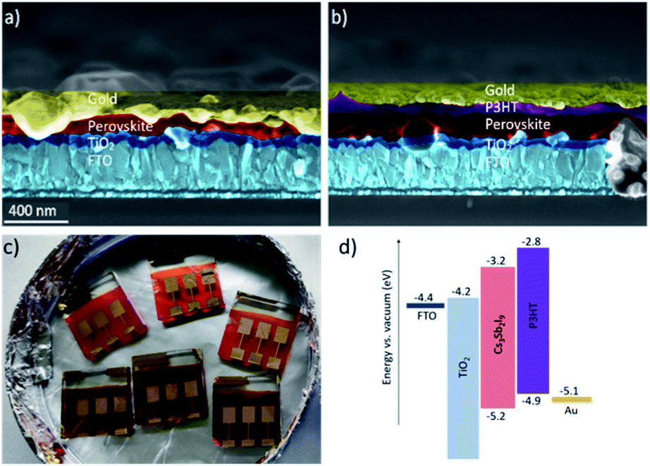 | ||
| Fig. 1 SEM images of the solar cell cross sections of Cs3Sb2I9 films without (a) and with P3HT (b). Photograph of the solar cells. (c) Size of the substrates is 2 cm × 2 cm and active area 20 mm2. Photos of perovskite/P3HT films are shown in the ESI.† Energy levels diagram for the key components of the solar cells (d). | ||
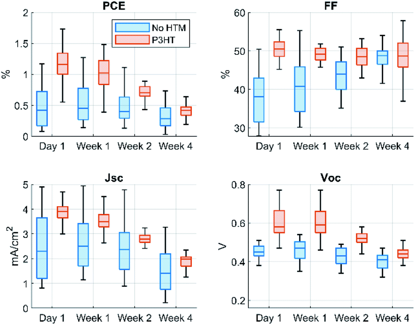
The improvement obtained with the P3HT hole transport layer is presented in Fig. 2 and Table 1. The open-circuit voltage (VOC), short-circuit current (JSC), and FF were all improved, which resulted in doubled power conversion efficiency. The greatest improvement was observed in VOC, which increased on average by 43% while JSC increased by 27% and FF 17%. In absolute values, the increase in VOC was 0.2 V, and for our best device we measured 0.8 V for VOC. The major improvement in VOC is particularly important for antimony perovskite solar cells as they typically suffer from low voltages.
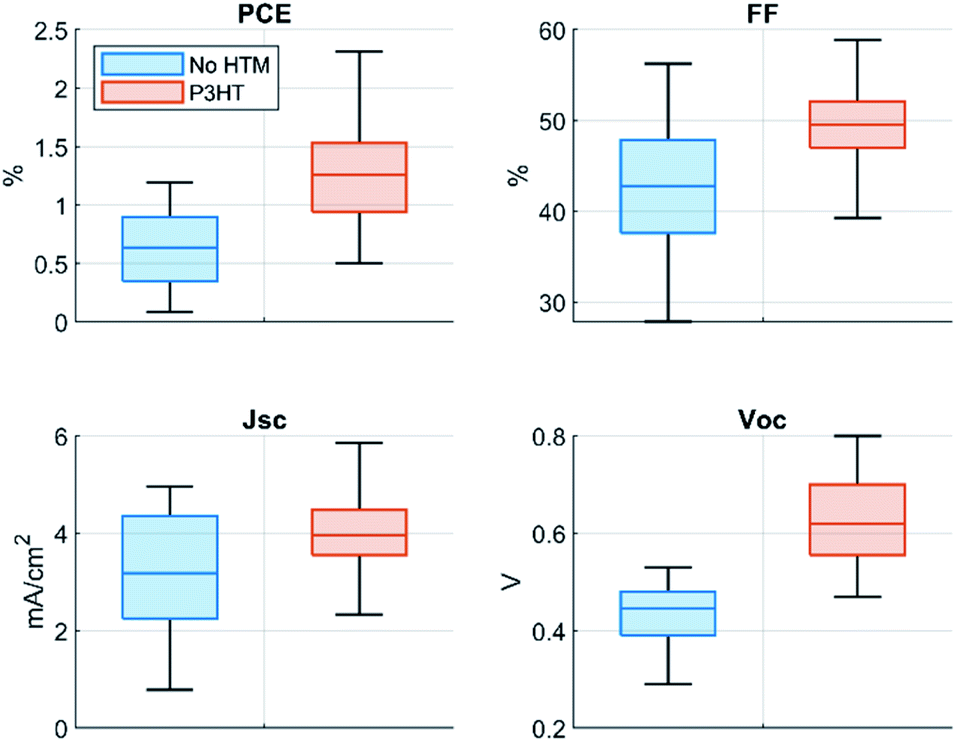 | ||
| Fig. 2 Statistical presentation of the improvement resulting from P3HT hole transport layer incorporation. The colored box represent 25% upper and lower bound (i.e. the interquantile range; IQR) from the median which is denoted by the horizontal line in the middle of the box. The black lines represent the values that are not further than 1.5 × IQR from the top or bottom of the box. | ||
| PCE (%) | FF (%) | J SC (mA cm−2) | V OC (V) | |
|---|---|---|---|---|
| P3HT | 1.29 | 49.24 | 3.98 | 0.63 |
| Stdev | 0.46 | 3.98 | 0.80 | 0.09 |
| Best | 2.48 | 54.90 | 5.40 | 0.80 |
| No HTM | 0.62 | 42.09 | 3.13 | 0.44 |
| Stdev | 0.33 | 7.55 | 1.29 | 0.06 |
| Best | 1.19 | 47.70 | 4.70 | 0.52 |
The best device gave 2.48% PCE in the reverse scan (see Fig. 3a) for the current–voltage curve (JV-curve), while the reference solar cells without P3HT did yield 1.19% PCE for the champion device (average PCE of 0.62%), being in good accordance with the literature.9 The comparison between the photovoltaic parameters of our solar cells and those of state-of-the-art devices with inorganic Sb-perovskite absorber demonstrates the superior performance achieved in this work (see Table S1 in ESI, ESI†).
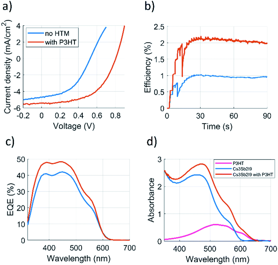 | ||
| Fig. 3 (a) JV-curves, (b) 1 minute MPP-tracking (c) EQE (d) UV-Vis absorbance of the solar cells with and without P3HT. | ||
The devices show large hysteresis but the improvement obtained with the P3HT remains constant in both scan directions. Forward and reverse scans are shown in the Fig. S1 (ESI).† Knowing that perovskite-type solar cell's PCE is sensitive to the JV-curve sweep rate and direction, we performed maximum power point tracking (MPPT) for the best devices.20 The MPP-tracked PCE for the best device using P3HT was 2.0% averaged over 60 s (Fig. 3b). No MPP-tracking for Cs3Sb2I9 solar cells has so far been reported in the literature, hence this result serves as an important benchmark in reporting antimony perovskite solar cell efficiencies. The MMP-tracked efficiency for the reference solar cell without P3HT was 0.9%.
The excellent performance of the P3HT as a hole transport material could be due to the well-matched energy level alignment between the P3HT and Cs3Sb2I9. The valence band (VB) of Cs3Sb2I9 has been reported to lie at −5.16 eV9 and that of the P3HT is at −5.0 eV21 making them a suitable match with minimized losses in the VOC. Recently P3HT was found to overperform spiro-OMeTAD (PCE = 1.62% for P3HT device against 1.12% for spiro-OMeTAD analogue) when used as hole transport layer together with (CH3NH3)3Bi2I9.22 The improved performance was as well attributed to the good energy level alignment between the P3HT and the perovskite.
In literature, prior to this work, a few other hole transport materials in addition to P3HT have been tested together with Cs3Sb2I9 and its derivatives. Peng et al. compared poly-TPD against LZ-HTL-1-1 in Cs3Sb2ClxI9−x based devices.19 In particular for the 2D Cs3Sb2Cl3I6 the LZ-HTL-1-1 improved the JSC and FF significantly but slightly reduced the VOC resulting still in an overall performance improvement. Their best device with LZ-HTL-1-1 gave 6.46 mA cm−2JSC, 55.7% FF, 0.6 V VOC and 2.15% PCE. The superiority of LZ-HTL-1-1 over poly-TPD was attributed to the sevenfold higher hole mobility. Yang et al. successfully used doped spiro-OMeTAD as HTM in a MA3Sb2ClxI9−x based device.13 Their optimized device gave JSC of 7.38 mA cm−2, VOC of 0.70 V, FF of 0.65, and PCE of 3.34%. Comparing our work with the above mentioned works should be done with caution as the active layers are different, however, it appears that spiro-OMeTAD can deliver highest JSC and FF while P3HT significantly improves the voltage.
External quantum efficiencies (EQE) were measured to examine the function of P3HT in the devices (Fig. 3c). The Cs3Sb2I9 has an optical absorption onset at 600 nm while that of P3HT has it at 650 nm as seen in Fig. 3d (absorption spectrum converted to Tauc plot is given in the ESI, Fig. S3†). However, no difference is observed between the devices at EQE onset indicating that the P3HT does not take part in photocurrent generation via broadened absorption bandwidth. Therefore, we suggest that P3HT improves the Cs3Sb2I9–gold interface via faster charge transfer kinetics. It is worth noting that, as P3HT has its LUMO level 0.4 eV (see Fig. 1d) above that of the conduction band of Cs3Sb2I9, it creates an injection barrier for electrons trying to travel from the conduction band of Cs3Sb2I9 towards the P3HT which as well contributes to the good HTM functioning of the P3HT. Fig. 4a compares the room-temperature (RT) steady-state photoluminescence (PL) spectra of glass/Cs3Sb2I9 and glass/Cs3Sb2I9/P3HT films. The films were excited from the glass side at 405 nm and the emission was detected in a reflection mode, aiming to minimize the excitation and emissive signal of P3HT film. The PL spectrum of pure Cs3Sb2I9 exhibits a broad and skewed emission band with a peak at 650 nm, due to the formation of the so-called self-trapped exciton (STE) induced emission in the range of long wavelength (>725 nm) observed previously in 2D Cs3Sb2I9 films at RT.23,24 The wide PL band of 2D Cs3Sb2I9 is further interpreted with the convolution of band edge emission (direct transition), STE emission, and defect-assisted emission, which has also been observed for recently reported 2D Cs3Sb2I9−xClx.8 A clear PL quenching is observed after coating P3HT on top of the Cs3Sb2I9 layer, indicating that a hole injection from the VB of Cs3Sb2I9 to the HOMO level of P3HT has occurred. This hole injection reaction is also observed by comparing the time-resolved PL (TRPL) decay for glass/Cs3Sb2I9/P3HT with that for glass/Cs3Sb2I9 in Fig. 4b. Both decays could be well fitted with a bi-exponential function and the fitting results are summarized in Table S2 (ESI).† The PL decay for glass/Cs3Sb2I9/P3HT shows a clear acceleration for both components (τ1 and τ2) compared to the excited state decay for pure Cs3Sb2I9 (glass/Cs3Sb2I9), indicating that the insertion of P3HT as HTM in between Cs3Sb2I9 layer and gold electrode indeed facilitates the efficient hole extraction and transport. The swift hole injection also suggests that the well-aligned VB of Cs3Sb2I9 with the HOMO level of P3HT could provide sufficient driving force to split the excitons for their efficient charge separation, leading to a large increase in VOC as previously observed.25
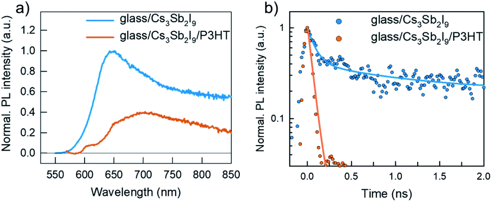 | ||
| Fig. 4 (a) Steady-state photoluminescence (PL) spectra and (b) time-resolved PL (TRPL) decays of glass/Cs3Sb2I9 and glass/Cs3Sb2I9/P3HT films, excited at 405 nm (excitation intensity ∼20 nJ cm−2 and time resolution ∼60 ps). Solid lines show the results of fitting with a bi-exponential function: IPL(t) = A1 × e(−t/τ1) + A2 × e(−t/τ2). | ||
The stability of the devices was monitored over a period of 1 month in ambient conditions. During this time the P3HT containing devices degraded 66% down to the level of the reference devices in terms of PCE (see Fig. 5 and Table 2). The numerical presentation of the data of Fig. 5 is given in ESI, Table S4.† The drop is seen most clearly in JSC and VOC which initially had the highest improvement pointing towards P3HT instability. However, the P3HT is reportedly stable during storage when paired with a suitable counterpart: together with PCBM or O-IDTRB the P3HT-based organic solar cells can keep more than 70% of their initial efficiency when stored in dark under ambient conditions.26 The photo degradation of pristine P3HT is known to proceed rapidly but when blended with the right acceptor the ageing processes are nearly suppressed.27 The acceptor materials protect the P3HT by quenching the reactive excited states on P3HT in the sub-nanosecond timescale.28 Therefore it appears that as such the Cs3Sb2I9 is not able to protect the P3HT from degradation possible due to too slow quenching of the P3HT singlet state. However, an unwanted reaction between the perovskite and the P3HT cannot be ruled out either. Such events could be resolved by modification of the P3HT perovskite interface. Recently Jung et al. used this approach for highly efficient (PCE 22.7%) lead-perovskite solar that had P3HT HTM. Their devices could keep 85% of their initial PCE for over 1000 h without encapsulation.29
 | ||
| Fig. 5 Statistical presentation of the solar cell's stability during 1 month of storage in air at dark at 20–21 °C. | ||
| No HTM | PCE | FF | J SC | V OC |
|---|---|---|---|---|
| Week 1 | 17 | 8 | 7 | 3 |
| Week 2 | 1 | 15 | −4 | −3 |
| Week 4 | −33 | 25 | −38 | −10 |
| With P3HT | PCE | FF | J SC | V OC |
|---|---|---|---|---|
| Week 1 | −12 | −3 | −10 | 0 |
| Week 2 | −41 | −3 | −29 | −13 |
| Week 4 | −66 | −2 | −52 | −27 |
It is interesting to note that the FF of the reference devices improved by 25% during the 1 month storage which to some degree compensated the losses in JSC which went down by 38%. Overall, the PCE of the reference devices dropped by 33%. The stability of PCE has been previously reported but has not been broken down into the FF, VOC, and I JSC. According to literature the layered form of Cs3Sb2I9 has good stability in ambient conditions while the dimer form degrades more rapidly.9,23,30 It is possible that some of the films that we monitored in this work were not fully converted to the 2D layered form. We monitored a rather large set of solar cells (38 devices in total) therefore it is likely that some of the devices contain imperfections such as incomplete crystallization.
In addition to the 1 month shelf-life stability, we performed 1 hour of light soaking at the maximum power point for both types of devices (see Fig. 6). The P3HT containing device decays steadily to a level of 85% from the initial value within the first 1.5 minutes after which the decay slows down and after 1 hour 82% of initial PCE remains. The device without P3HT is again more stable and can keep 95% of the initial PCE after 1 hour of light soaking.
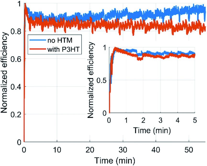 | ||
| Fig. 6 Light soaking (1 h) for the solar cells with and without P3HT. The inset shows the first 5 minutes. | ||
Experimental
Device fabrication
The Cs3Sb2I9 perovskite precursor was prepared according to Umar et al.9 with slight adjustments. The compound was mixed from CsI (99.999% from ABCR) and SbI3 (99.999% from Fisher) in a stoichiometric ratio. The powders were dissolved to a concentration of 444 mg ml−1 in N,N-dimethylformamide (Alfa Aesar, anhydrous 99.8%) containing 5% of hydrochloric acid (fuming ≥37% from Merck Sigma-Aldrich). The typical amount prepared was 50 μl of acid in 1 ml of DMF. According to Umar et al.,9 the optimum hydrochloric acid concentration was 3% while we found the optimum concentration to be 5%. The difference might arise in differences in the hydrochloric acid concentration, which might dilute during storage. The precursor was prepared inside a N2-filled glove box except the acid, which was added into the DMF outside of the glove box.The solar cells were fabricated onto FTO (fluorine-doped tin oxide) substrates (TEC15 2.2 mm thick from Greatcell Solar Materials) which were cut into 2 cm × 2 cm squares. The substrates were patterned by sprinkling a thin layer of zinc powder onto the part of FTO to be removed. Other parts of the FTO were protected with tape (Scotch Magic Tape). Then the substrates were bathed in 2 M HCl solution for 5 min after which the zinc powder was brushed away with a toothbrush while still in the bath. The substrates were subsequently cleaned with soap and water, followed by sonication in ultrapure water (Milli-Q), acetone, and 2-propanol for 15 min in each solvent. A compact titanium dioxide layer was deposited onto the cleaned FTO substrates by spray pyrolysis. The precursor used in the spraying was made of titanium diisopropoxide bis(acetylacetonate) 75 wt% in isopropanol (from Merck Sigma-Aldrich), which was further diluted with 2-propanol (Honeywell ≥99.8%). Typical amounts were 1.5 ml of titanium diisopropoxide bis(acetylacetonate) 75 wt% per 6.5 ml 2-isopropanol. The spraying was performed on a hotplate at 450 °C and consisted of 13 short sprays of precursor keeping a 20 s pause after each spraying. Having sprayed the final layer, the substrates were further annealed for 45 min at 450 °C up to the complete crystallization. The resulting TiO2 thickness was approximately 70 nm. The TiO2 substrates were stored in darkness until needed and treated with O2 plasma (from Harrick Plasma) for 1 min at medium power prior to perovskite precursor deposition.
The perovskite precursor solution was spin-coated onto the TiO2 coated substrates inside the N2 glove box. 35 μl of the precursor solution was pipetted onto the substrate after which the program was started (3000 rpm, 30 s, acceleration within 5 s). Approximately 15 seconds prior to the end of the program, at a point where the film begins to turn orange, 80 μl of isopropanol (anhydrous 99.5% from Merck Sigma-Aldrich) was pipetted onto the spinning substrate. After spin-coating was finished, the samples were placed onto a hotplate at 230 °C for 10 minutes.
The P3HT i.e. poly(3-hexylthiophene-2,5-diyl) (from Rieke Metals, Electronic Grade, Regioregular) was spin-coated from a 20 mg ml−1 solution of chlorobenzene (anhydrous 99.8% from Merk Sigma-Aldrich) onto the films inside the glove box. The solution was spin-coated dynamically i.e. at speed (2000 rpm, 30 s). The method was adopted from literature.31
Finally, 100 nm thick gold electrode was thermally evaporated (Edwards Auto 306) on the films inside a vacuum chamber pumped down to 5 × 10⁻⁶ mbar. One substrate carried 3 solar cells (area of each device was 20 mm2).
Solar simulation and JV-curves characterization
The JV-curves, the stability tests, and MPP-tracking were performed under 1 Sun illumination (100 mW cm−2), which was set with a Newport KG5 filtered reference cell (91150-KG5 Reference Cell and Meter). Measurements were carried out in ambient conditions and the solar cells had no encapsulation. The solar simulator was OAI TriSol 7 kW CPV-simulator with an AM0 filter. The JV-curves and the MPP-tracked efficiency were measured using a Keithley 2450 source meter unit in a 4-wire setup. The JV-curves were swept at a 50 mV s−1 rate. MPP-tracking was performed with a hill climbing algorithm measuring average power over 2 s intervals to determine voltage step direction. Tracking started from 0 V in 0.1 V steps until a maximum had been reached. Subsequently, the voltage was adjusted in 0.01 V steps towards the MPP. For the 1 month stability study, samples were stored in an air-conditioned laboratory at 20–21 °C. The samples were inside Petri dishes covered with aluminium foil to keep the samples in dark.Conclusions
We have shown that P3HT can be used as an efficient hole transport material for Cs3Sb2I9 solar cells without any doping. On average the efficiencies were doubled when P3HT was incorporated into the devices. The champion device had 2.5% PCE, which is the highest reported to date for cells employing Cs3Sb2I9 perovskite-inspired material. In addition, we presented for the first time MPPT data for this type of solar cells; the MPP-tracked PCE was 2.0%. As hole transport layers are essential for efficient solar cell function, we hope these results will contribute to close the gap between lead-free and lead-based perovskite solar cell performance. Significant degradation occurred during 1 month storage, hence we suggest that further research should look into making the perovskite-P3HT interface stable.Electron microscopy
The electron microscope images were taken with Zeiss UltraPlus FE-SEM instrument operated at 3 kV acceleration voltage in inlens mode.PL, TRPL and UV-Vis measurements
Steady-state PL spectra were measured with a FLS1000 spectrofluorometer (Edinburgh Instruments, UK). The TRPL decays were recorded with a time-correlated single photon counting (TCSPC) apparatus equipped with a Picoharp 300 controller and a PDL 800-B driver for excitation and a Hamamatsu R3809U-50 microchannel plate photomultiplier for detection in a 90° configuration. The UV-Vis spectra were recorded with Shimadzu UV-1900i spectrophotometer.Author contributions
A. H. and N. L. contributed equally. A. H. conceived the experiments, fabricated the solar cells, performed SEM imaging, and wrote the first draft of the manuscript. N. L. contributed to the film characterization, solar cell fabrication, writing and revising the manuscript. H. S. carried out the MPP-tracking experiments. M. L. performed the PL/TRPL characterization and analysis. P. V. supervised the work, acquired funding, and contributed in writing/revising the manuscript.Conflicts of interest
There are no conflicts to declare.Acknowledgements
A. H. and P. V. thank Academy of Finland (Decision No. 319042). P. V. and N. L. also acknowledge Jane & Aatos Erkko foundation (project: ASPIRE). M. L. thanks Finnish Cultural Foundation (00210670) for funding. This work is part of the Academy of Finland Flagship Programme, Photonics Research and Innovation (PREIN), Decision No. 320165.References
- L. Chouhan, S. Ghimire, C. Subrahmanyam, T. Miyasaka and V. Biju, Chem. Soc. Rev., 2020, 49, 2869–2885 RSC.
- NREL, Best Research-cell Efficiency Chart, https://www.nrel.gov/pv/cell-efficiency.html, accessed 15th October 2021 Search PubMed.
- A. Abate, Joule, 2017, 1, 659–664 CrossRef CAS.
- V. Pecunia, L. Occhipinti and R. L. Z. Hoye, Adv. Energy Mater., 2021, 11, 2100698 CrossRef CAS.
- Y. T. Huang, S. R. Kavanagh, D. O. Scanlon, A. Walsh and R. L. Z. Hoye, Nanotechnology, 2021, 32, 132004 CrossRef CAS.
- N. Giesbrecht, A. Weis and T. Bein, J. Phys. Energy, 2020, 2, 024007 CrossRef CAS.
- J.-P. Correa-Baena, L. Nienhaus, R. C. Kurchin, S. Sik Shin, S. Wieghold, N. T. Putri Hartono, M. Layurova, N. D. Klein, J. R. Poindexter, A. Polizzotti, S. Sun, M. G. Bawendi and T. Buonassisi, Chem. Mater., 2018, 30, 3734–3742 CrossRef CAS.
- J. Mei, M. Liu, P. Vivo and V. Pecunia, Adv. Funct. Mater., 2021, 2106295 CrossRef.
- F. Umar, J. Zhang, Z. Jin, I. Muhammad, X. Yang, H. Deng, K. Jahangeer, Q. Hu, H. Song and J. Tang, Adv. Opt. Mater., 2019, 7, 1801368 CrossRef.
- B. Saparov, F. Hong, J.-P. Sun, H.-S. Duan, W. Meng, S. Cameron, I. G. Hill, Y. Yan and D. B. Mitzi, Chem. Mater., 2015, 27(16), 5622–5632 CrossRef CAS.
- Z. Xiao, Z. Song and Y. Yan, Adv. Mater., 2019, 31, 1803792 CrossRef CAS PubMed.
- M. Saliba, T. Matsui, J.-Y. Seo, K. Domanski, J.-P. Correa-Baena, M. K. Nazeeruddin, S. M. Zakeeruddin, W. Tress, A. Abate, A. Hagfeldt and M. Grätzel, Energy Environ. Sci., 2016, 9, 1989–1997 RSC.
- Y. Yang, C. Liu, M. Cai, Y. Liao, Y. Ding, S. Ma, X. Liu, M. Guli, S. Dai and M. K. Nazeeruddin, ACS Appl. Mater. Interfaces, 2020, 12, 17062–17069 CrossRef CAS PubMed.
- N. Gluck and T. Bein, Energy Environ. Sci., 2020, 13, 4691–4716 RSC.
- F. Li, Y. Wang, K. Xia, R. L. Z. Hoye and V. Pecunia, J. Mater. Chem. A, 2020, 8, 4396–4406 RSC.
- P. C. Harikesh, H. Kumar Mulmudi, B. Ghosh, T. W. Goh, Y. T. Teng, K. Thirumal, M. Lockre, K. Weber, T. Ming Koh, S. Li, S. Mhaisalkar and N. Mathews, Chem. Mater., 2016, 28(20), 7496–7504 CrossRef CAS.
- K. Moorthy Boopathi, P. Karuppuswamy, A. Singh, C. Hanmandlu, L. Lin, S. Ali Abbas, C. Cheng Chang, P. Cheng Wang, G. Li and C. Wei Chu, J. Mater. Chem. A, 2017, 5, 20843 RSC.
- A. Singh, K. M. Boopathi, A. Mohapatra, Y. F. Chen, G. Li and C. W. Chu, ACS Appl. Mater. Interfaces, 2018, 10, 2566–2573 CrossRef CAS.
- Y. Peng, F. Li, Y. Wang, Y. Li, R. L. Z. Hoye, L. Feng, K. Xia and V. Pecunia, Appl. Mater. Today, 2020, 19, 100637 CrossRef.
- J. A. Christians, J. S. Manser and P. V. Kamat, J. Phys. Chem. Lett., 2015, 6, 852–857 CrossRef CAS PubMed.
- W. C. Tsoi, S. J. Spencer, L. Yang, A. M. Ballantyne, P. G. Nicholson, A. Turnbull, A. G. Shard, C. E. Murphy, D. D. C. Bradley, J. Nelson and J. S. Kim, Macromolecules, 2011, 44, 2944–2952 CrossRef CAS.
- S. M. Jain, T. Edvinsson and J. R. Durrant, Commun. Chem., 2019, 2, 1 CrossRef CAS.
- B. Saparov, F. Hong, J. P. Sun, H. S. Duan, W. Meng, S. Cameron, I. G. Hill, Y. Yan and D. B. Mitzi, Chem. Mater., 2015, 27, 5622–5632 CrossRef CAS.
- K. M. McCall, C. C. Stoumpos, S. S. Kostina, M. G. Kanatzidis and B. W. Wessels, Chem. Mater., 2017, 29, 4129–4145 CrossRef CAS.
- M. Stolterfoht, P. Caprioglio, C. M. Wolff, J. A. Márquez, J. Nordmann, S. Zhang, D. Rothhardt, U. Hörmann, Y. Amir, A. Redinger, L. Kegelmann, F. Zu, S. Albrecht, N. Koch, T. Kirchartz, M. Saliba, T. Unold and D. Neher, Energy Environ. Sci., 2019, 12, 2778–2788 RSC.
- S. Holliday, R. S. Ashraf, A. Wadsworth, D. Baran, S. A. Yousaf, C. B. Nielsen, C. H. Tan, S. D. Dimitrov, Z. Shang, N. Gasparini, M. Alamoudi, F. Laquai, C. J. Brabec, A. Salleo, J. R. Durrant and I. McCulloch, Nat. Commun., 2016, 7, 1–11 Search PubMed.
- M. Manceau, S. Chambon, A. Rivaton, J. L. Gardette, S. Guillerez and N. Lematre, Sol. Energy Mater. Sol. Cells, 2010, 94, 1572–1577 CrossRef CAS.
- M. Jørgensen, K. Norrman, S. A. Gevorgyan, T. Tromholt, B. Andreasen and F. C. Krebs, Adv. Mater., 2012, 24, 580–612 CrossRef PubMed.
- E. H. Jung, N. J. Jeon, E. Y. Park, C. S. Moon, T. J. Shin, T. Y. Yang, J. H. Noh and J. Seo, Nature, 2019, 567, 511–515 CrossRef CAS PubMed.
- T. D. Chonamada, A. B. Dey and P. K. Santra, ACS Appl. Energy Mater., 2020, 3, 47–55 CrossRef CAS.
- L. Yang, U. B. Cappel, E. L. Unger, M. Karlsson, K. M. Karlsson, E. Gabrielsson, L. Sun, G. Boschloo, A. Hagfeldt and E. M. J. Johansson, Phys. Chem. Chem. Phys., 2012, 779–789 RSC.
Footnotes |
| † Electronic supplementary information (ESI) available. See DOI: 10.1039/d1se01150b |
| ‡ These authors contributed equally to this work. |
| This journal is © The Royal Society of Chemistry 2022 |