
 Open Access Article
 This Open Access Article is licensed under a
 Creative Commons Attribution 3.0 Unported Licence
Chloro aluminum phthalocyanine-based organic thin-film transistors as cannabinoid sensors: engineering the thin film response†
Halynne R.
Lamontagne
ab,
Zachary J.
Comeau
ab,
Rosemary R.
Cranston
 a,
Nicholas T.
Boileau
a,
Cory S.
Harris
bc,
Adam J.
Shuhendler
*bcd and
Benoît H.
Lessard
*ae
a,
Nicholas T.
Boileau
a,
Cory S.
Harris
bc,
Adam J.
Shuhendler
*bcd and
Benoît H.
Lessard
*ae
aDepartment of Chemical and Biological Engineering, University of Ottawa, 161 Louis Pasteur, Ottawa, ON K1N 6N5, Canada. E-mail: Benoit.Lessard@uottawa.ca
bDepartment of Chemistry and Biomolecular Sciences, University of Ottawa, 150 Louis Pasteur, Ottawa, ON, K1N 6N5 Canada. E-mail: Adam.Shuhendler@uottawa.ca
cDepartment of Biology, University of Ottawa, 30 Marie Curie, Ottawa, ON, K1N 6N5 Canada
dUniversity of Ottawa Heart Institute, 40 Ruskin St, Ottawa, ON, K1Y 4W7 Canada
eSchool of Electrical Engineering and Computer Science, University of Ottawa, 800 King Edward Ave., Ottawa, ON K1N 6N5, Canada
First published on 10th August 2022
Abstract
Cannabis producers, retailers, and law enforcement increasingly need low-cost point-of-source cannabinoid sensors. Organic thin-film transistor (OTFT) based sensors are a promising technology that can provide rapid speciation and detection of Δ9-tetrahydrocannabinol (THC) while maintaining low manufacturing costs and ease of use. Herein, chloro aluminum phthalocyanine (Cl-AlPc) OTFTs were optimized through engineering film thickness (30, 50 or 100 nm) and the device source-drain geometry (W/L = 100, 200, 400, 800 and 1000), as these parameters have been shown to strongly influence OTFT performance. Optimized Cl-AlPc OTFT based sensors were exposed to both THC solution and THC vapor, demonstrating that improved device performance was not directly correlated with increased sensitivity. Grazing-incidence wide-angle X-ray scattering (GIWAXS) and atomic force microscopy (AFM) were used to interrogate thin-film morphology. While little change in molecular orientation resulted from film thickness or exposure to THC, the data suggests that the improved sensing response of Cl-AlPc-derived devices is directly related to increased thin-film surface area resulting from increased roughness and reduced film thickness.
Introduction
In recent years, recreational and medicinal cannabis (Cannabis sativa) use has been growing in popularity, with countries increasingly removing restrictions on its consumption and sale.1 The psychotropic effects commonly associated with cannabis are caused by cannabinoids produced in the plant, most notably Δ9-tetrahydrocannabinolic acid (THCA) that, upon heating, decarboxylates to Δ9-tetrahydrocannabinol (THC), which is known to cause psychogenic effects in consumers.2 THC is chemically very similar to other cannabinoids in cannabis products, including some that are potentially therapeutic, such as cannabidiol (CBD).2 Due to this chemical similarity, it is difficult to differentiate THC and CBD in consumer products or human biological samples, which presents a challenge for a variety of cannabis-related fields, including cannabis producers, government regulatory bodies, law enforcement, and medical professionals. The current state-of-the-art detection methods used in industry, such as high-performance liquid chromatography (HPLC), have a high level of sensitivity but are expensive, time-consuming, require specialists to interpret the results, and cannot be performed on-the-spot.3 Thus, there is a present need for low-cost point-of-source sensors that maintain both accuracy and a high level of sensitivity. Organic thin-film transistor (OTFT)-based sensors are a promising alternative that offer fast and accurate detection of cannabinoids while being accessible, disposable, and inexpensive.4–6 OTFTs have the potential to achieve a lower manufacturing cost than conventional electronics, as OTFTs utilize more affordable organic materials and are manufactured at ambient temperatures. The simple device structure of an OTFT also makes them conducive to high-volume manufacturing processes, like roll-to-roll printing.7–14 OTFTs are three-electrode solid state electrical devices where current travels at the interface between an organic semiconductor and a dielectric. Changes in electrical behaviour can result from several mechanisms, including oxidation/reduction, and doping or physical changes in the active semiconducting material.15–20 Understanding which mechanisms contribute to sensing and how these mechanisms interact will enable the optimization and enhancement of OTFT based sensors.Metal and metalloid phthalocyanines (MPcs) are a class of conjugated macrocyclic molecules that have found success as semiconducting layers in OTFTs21,22 and organic photovoltaics (OPVs).23,24 MPcs are thermally and chemically stable, inexpensive to manufacture on the ton scale with facile metal substitution providing opportunities to tune molecular interactions for integration into OTFT sensors.6,21,25–30 While many MPcs are insoluble or sparingly soluble in organic solvents, they can be modified with solubilizing groups making them potentially compatible with low-cost solution processing techniques. Previously, we demonstrated copper phthalocyanine (CuPc) OTFT sensors for ratiometric detection and differentiation of cannabinoids.6 Observed by spectroelectrochemistry and 2D NMR, cannabinoids interact strongly with MPcs in solution, and in thin-films, causing changes in Pc–Pc π-stacking and increasing π-electron delocalization.31 These interactions can induce recrystallization of MPc thin-films, altering thin-film morphologies and nanostructures, resulting in OTFT performance changes which enhance the detection of THC and lead to better sensitivity.26 The central aluminum chloride of chloro aluminum phthalocyanine (Cl-AlPc, Fig. 1) bends the MPc ring, resulting in unique packing structures that are susceptible to cannabinoid induced physical effects, demonstrating greater interactions both in solution and as a thin-film compared to CuPc.26,31 In bottom-gate bottom-contact (BGBC) OTFTs, the thickness of the deposited semiconductor film has been observed to effect OTFT charge transport properties.32–34 For evaporated small molecules, surface coverage, growth mode, and thin-film morphology can change with thickness, leading to altered charge transport properties.25,35–38 Thus, to increase the sensitivity of cannabinoid sensors, we exploit the sensitivity of Cl-AlPc to cannabinoids by altering the semiconducting layer and device architecture of Cl-AlPc-based OTFTs.
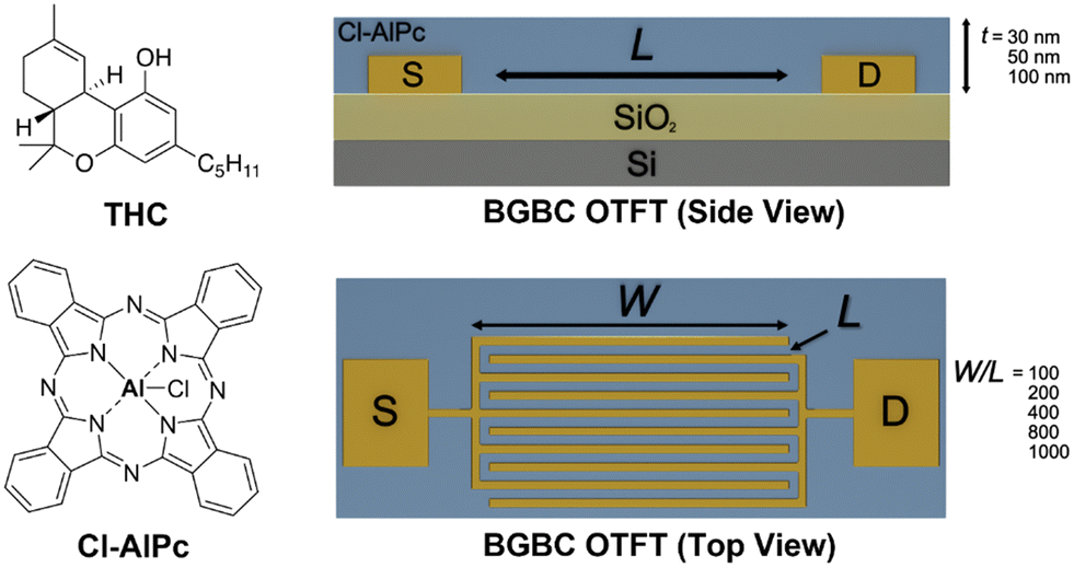 | ||
| Fig. 1 Chemical structure of chloro aluminum phthalocyanine (Cl-AlPc) and Δ9-tetrahydrocannabinol (THC), as well as a schematic representation of the bottom-gate bottom-contact (BGBC) organic thin-film transistor (OTFT) architecture used in this study. | ||
Towards the goal of understanding how to optimize Cl-AlPc-based devices for THC sensing, we studied the molecular interactions of Cl-AlPc in OTFTs and the structural alterations that take place upon exposure to cannabinoids in both liquid and vapor phases. By synchrotron grazing-incident wide-angle X-ray scattering (GIWAXS) and atomic force microscopy (AFM) we probe the nanostructures of Cl-AlPc thin-films, comparing the effects of OTFT architecture and thin-film thickness to overall OTFT sensor performance. In addition, we aim to determine if these parameters affect baseline device performance in the same way as sensor performance to differentiate the dynamics of THC sensing from normal OTFT operation. This work demonstrates that device architecture has little effect on sensor performance; instead, we find that film thickness substantially impacts both pre- and post-exposure device performance and sensitivity, particularly to THC solution. This illustrates the importance of deposition conditions and thin-film morphology.
Results and discussion
Baseline Cl-AlPc OTFT optimization
To examine the effects of device architecture on OTFT performance we prepared a series of BGBC Cl-AlPc-based OTFTs under identical evaporation conditions, with thin-film thicknesses of 30 nm, 50 nm or 100 nm and W/L ratios from 100 to 1000 on OTS treated Si/SiO2 substrates (Fig. 1). Characteristic transfer curves can be found in Fig. 2, along with plots of the on-current (Ion) and μh with the tested W/L ratios and film thicknesses. The output curves and a summary table can be found in Fig. S1 and Table S1,† respectively. A two-way ANOVA analysis was performed on the data shown in Fig. 2D and E to determine the significance of each pair-wise data set to a confidence of 95%, and the results can be found in Table S2.† As expected from eqn (1), Ion increases with increasing W/L, from approximately 100 μA to 5000 μA from a W/L of 100 to 1000. Additionally, Ion increases with increasing film thickness, yielding an increase in μh from 0.02 cm2 V−1 s−1 to 0.5 cm2 V−1 s−1, consistent with previously reported performances for Cl-AlPc devices.26,27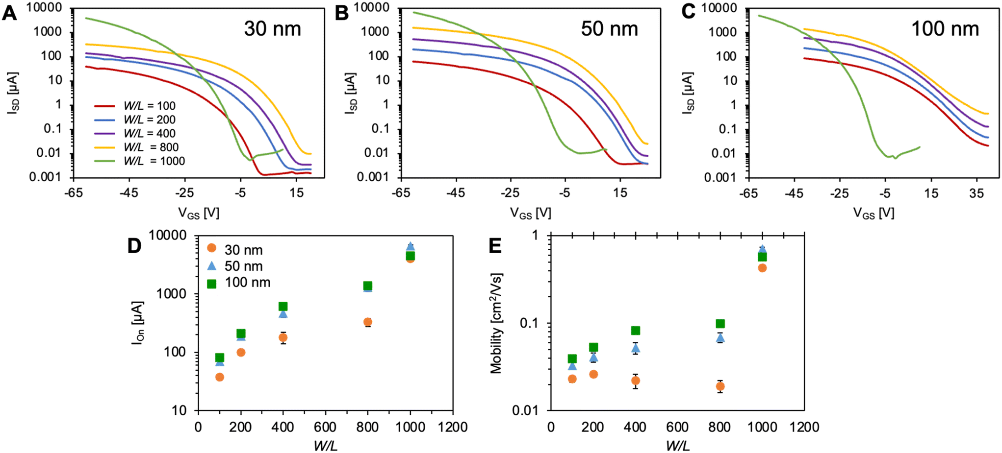 | ||
| Fig. 2 Transfer curves for Cl-AlPc devices with 30 nm (A), 50 nm (B), and 100 nm (C) thickness. Ion (D) and μh (E) are plotted with W/L and Cl-AlPc thickness. In panels D and E, points represent the means of a minimum of 4 devices and error bars represent standard deviation. Significance of data has been analyzed by two-way ANOVA and can be found in Table S2.† | ||
An ideal transfer curve would have a VT near 0, a low Ioff followed by a sharp increase in current after the VT (steep subthreshold slope), and the current would plateau at a high Ion resulting in a high Ion/off, with low hysteresis throughout the transfer curve. While a higher Ion led to a higher μh for the thicker films, the transfer curves for these films are less ideal. A greater VT, lower Ion/off, and a smaller subthreshold slope is observed for the 100 nm devices compared to the 30 nm devices. The Ion also increases as the W/L ratio increases from 100 to 800, while the transfer curves become less ideal. A W/L of 1000 shows the most ideal transfer curves with the highest Ion and μh. The devices with a W/L ratio of 1000 had the same L (10 μm) but a greater W (10 mm) than the devices with a W/L ratio of 200 (W = 2 mm), thus, the dependence of these metrics on W/L is likely a result of contact resistance, which becomes more dominant as L decreases.39,40 This increased contact resistance would lead to the less optimal transfer characteristics that we observed for higher W/L ratios. Additionally, there is a reduced effect from channel resistance in devices with a lower L,39,40 leading to higher operating currents. This resistance dominates in devices that have a greater L, which explains the lower performance of the devices with a lower W/L ratio. The design of the devices with the W/L of 1000 balances the channel and contact resistances to give high operating current with ideal transfer characteristics. This balance is illustrated by the VT of the devices in Fig. 2, where the VT increases from a W/L of 100 to 800 but drops for the W/L of 1000.
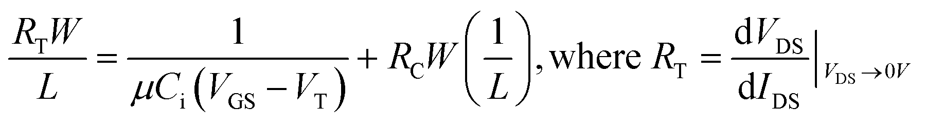
The contact resistance for each Cl-AlPc thickness was calculated as a function channel length using the modified-transfer length method (M-TLM)(eqn (2)), the results of which can be found in Table S3.† The contact resistance decreased with increasing film thickness. This supports the resulting higher Ion and μh observed for the 100 nm devices, as its contact resistance was the lowest, allowing for easier charge injection and higher mobilities.
Thin-films of Cl-AlPc, with thicknesses of 30 nm, 50 nm, or 100 nm, were characterized by GIWAXS with the resulting spectra shown in Fig. 3. These spectra reveal that the films are moderately semicrystalline and correspond well to the single crystal as demonstrated by the diffraction patterns shown in Fig. 3G. The high intensity (001) peak at approximately q = 0.5 Å−1, along the qz axis observed in all spectra indicates a major preferential orientation of molecules aligned parallel to the substrate. The distinct feature at χ = −30° observed in Fig. 3H indicate Cl-AlPc molecules aligned ∼30° to the substrate in a face-on configuration for all thin-film thicknesses. Although no change in molecular orientation is observed with film thickness, a loss of molecular order is exhibited in the thicker 100 nm films. Characterizing the surface morphology of the Cl-AlPc films by AFM, we observe the ordering of the grains improves with decreasing film thickness, supporting the observations from the GIWAXS spectra. The 30 nm film shows the most ordered grains and sharpest signals by GIWAXS, indicating the highest level of molecular order.
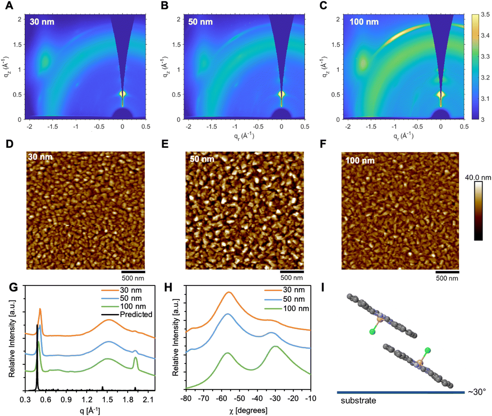 | ||
| Fig. 3 2D scattering patterns (θ = 0.3°) of (A) 30 nm, (B) 50 nm, and (C) 100 nm thick Cl-AlPc. Atomic force microscopy (AFM) images of (D) 30 nm, (E) 50 nm, and (F) 100 nm thick Cl-AlPc with scale bars of 500 nm. Diffraction pattern of Cl-AlPc (G) predicted from single crystal (CCDC #1134071)41 and 100 nm, 50 nm and 30 nm thick films determined by grazing-incidence wide-angle X-ray scattering (GIWAXS). Linecut profiles (H) of 100 nm, 50 nm, and 30 nm thick Cl-AlPc films with respect to χ using a q range between 1.9–2.1 Å−1. Molecular orientation (I) of Cl-AlPc relative to the substrate. | ||
The 30 nm films also demonstrated the best transfer characteristics in their corresponding devices, with high Ion/off ratios, low VT, and greater subthreshold slopes (Fig. 2). In contrast, the 100 nm film showed more disordered grains by AFM and broad GIWAXS signals, indicating a disordered morphology (Fig. 3). Though these films had high operating currents and low contact resistance, which yielded a high μh, they had the worst transfer characteristics with a high VT, hysteresis, and low subthreshold slope (Fig. 2). The 50 nm films appear significantly rougher than the other thicknesses, suggesting surface-ordered film growth up to ∼30 nm (RMS = 5.69 nm) which transitions to island growth up to ∼50 nm (RMS = 9.49 nm), yielding the observed roughness and grain order (Fig. 3). The islands fill in as the thickness approaches 100 nm (RMS = 5.06 nm), yielding the smoothest, but most disordered, films. Consequentially, the more ordered films will have improved charge transport pathways, however, the number of pathways available are likely lower. This will hinder charge injection and limit the operating current and μh as a result. Alternatively, the 100 nm films experience an increased number of charge transport pathways, making charge injection easier, giving rise to the higher μh and operating current in their corresponding devices. The disordered nature of the films and these pathways causes worse transfer characteristics. The 50 nm films strike a balance somewhere in between, experiencing both an increased number of charge transport pathways compared to the 30 nm film, and improved charge transport pathways compared to the 100 nm film. This leads to a high μh and operating current, while maintaining favorable transfer characteristics. Though thin-film morphology is conserved for all thicknesses, the degree of molecular order, and thus the OTFT characteristics, varies, with a >5-fold increase in mobility at the expense of other semiconducting properties. Thus, it is important to control the thickness of the Cl-AlPc film to control the grain morphology, charge transport properties, and baseline performance of Cl-AlPc OTFTs.
Cl-AlPc OTFT sensor optimization
In our previous studies,26,31 we identified that Cl-AlPc strongly interacts with THC, leading to large changes in OTFT performance. Thus, by exposing BGBC OTFTs with different Cl-AlPc film thicknesses (30 nm, 50 nm, and 100 nm) and two geometries (W/L = 200 and 1000) to both a liquid solution of THC and THC vapor, we could examine thin-film processing conditions and device architecture of Cl-AlPc OTFTs with the goal of establishing the greatest sensor response. Differences in VT, μh and Ion/off between OTFTs pre- and post-exposure are displayed in Fig. 4. Characteristic OTFT output curves and transfer curves post-THC exposure can be found in Fig. S2 and S3,† respectively. A two-way ANOVA was performed on the results to analyze their statistical significance to a 95% confidence level, and the results of the pair-wise comparisons can be found in Table S4.†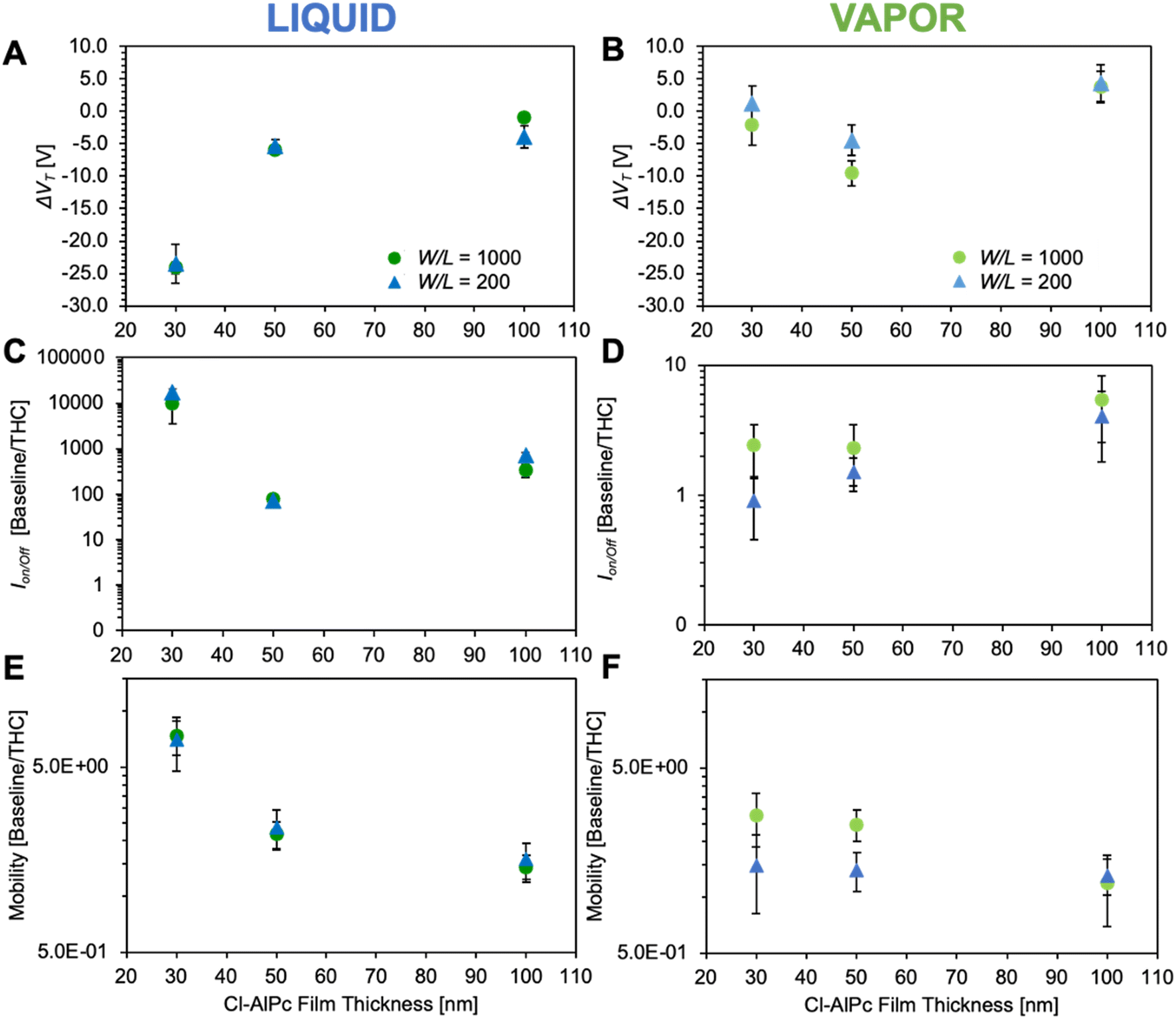 | ||
| Fig. 4 Cl-AlPc OTFT based sensor characteristics when exposed to THC solution (A, C, and E) and THC vapor (B, D and F). The device performance changes are reported difference from the baseline device and the exposed device for VT, (A and B), and a ratio from the baseline and the exposed device for Ion/off, (C and D), and μh, (E and F). The axes of (C) and (D) have been plotted on different scales to better frame the data. Points represent the means of a minimum of 4 devices and error bars represent standard deviation. Significance of data has been analyzed by two-way ANOVA and can be found in Table S3.† | ||
As illustrated in Fig. 4, exposure to THC solution led to a reduction in VT, μh and Ion/off for all devices, however a significantly larger change was observed for the 30 nm devices, indicating that a thinner semiconductor layer is more sensitive to THC in solution. The devices were less sensitive to THC vapor; although a slight reduction in Ion/off current was still observed, with no trend as a function of film thickness. A reduction in μh was also observed in response to THC vapor, with a greater response from the 30 nm film compared to the 100 nm film. This result was expected, as previous OTFT gas sensors have shown greater sensitivities with thinner semiconductor films.32,42,43 Channel architecture (W/L) did not appear to influence OTFT performance when exposed to THC solution. Contrastingly, the W/L appears to have a slight effect on the sensitivity of the OTFTs to vapor THC. The W/L of 1000 exhibited marginally larger changes in VT, Ion/off, and μh, with this effect more pronounced in the thinner films than the 100 nm film. This was determined to be statistically significant. This effect has been demonstrated previously, where channels with larger widths lead to more sensitive gas sensors due to their larger surface area for sensing interactions to occur.44 Exposing the OTFTs to pure hexanes as a blank solvent control leads to no change in device performance, as we have previously illustrated.6 This suggests that the Cl-AlPc OTFTs are sensitive not only to the analyte but also the form in which the analyte is exposed to the sensor. In both forms of THC exposure, vapor and solution, the devices with the more ideal baseline transfer curves led to the greater response; the 30 nm devices or a W/L of 1000.
The same experiments were performed with solution and vapor CBD, the results of which can be found in Fig. S4.† The sensitivity to CBD was similarly strongly dependent on film thickness, particularly to solution samples, while the channel architecture had little to no effect on sensitivity.
Cl-AlPc films were further characterized by GIWAXS post-exposure to THC solution and vapor with their spectra shown in Fig. 5 and S5.† For the 30 nm films, the primary alignment of the molecules remains at 30° to the substrate surface, and no new molecular orientations appear upon exposure to THC. However, the corresponding AFM images in Fig. 5, show a slight increase in grain sizes and disordering after exposure to THC, with some slight roughening of the films from RMS = 5.69 nm to RMS = 6.57 nm for samples exposed to THC solution and RMS = 7.11 nm for samples exposed to THC vapor, with similar trends observed for the 100 nm films (Fig. S5†).
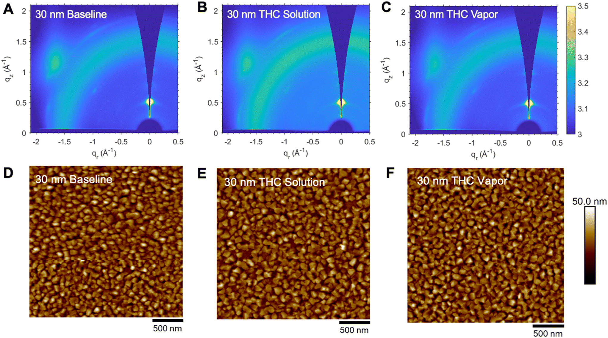 | ||
| Fig. 5 2D scattering patterns (θ = 0.3°) of (A) unexposed baseline, (B) THC solution exposed, and (C) THC vapor exposed 30 nm thick Cl-AlPc. AFM images of (D) unexposed baseline, (E) THC solution exposed, and (F) THC vapor exposed 30 nm thick Cl-AlPc with scale bars of 500 nm. | ||
Unlike the 30 nm and 100 nm films, the 50 nm films by GIWAXS demonstrated some molecular reorganization upon exposure to a liquid THC solution and THC vapor as shown in Fig. 6. Upon exposure to liquid THC solution, the film appeared to become more ordered, reflected by the sharper signals in the GIWAXS spectra and diffraction patterns. This can also be observed in the AFM images. The roughness of the film decreased from a baseline of RMS = 9.49 nm to 8.02 nm after exposure, resulting in a more uniform, ordered film upon exposure to THC in solution. The vapor-exposed film also experienced a slight decrease in surface roughness (RMS = 8.86 nm) and increase in grain order. Addtionally, the 50 nm vapor-exposed films demonstrated small changes in the molecular orientation of Cl-AlPc, with a slight shift of the (004) peak from a baseline of q = 1.92 Å−1 to q = 1.85 Å−1 (Fig. S6†). This suggests that the rougher grains of the 50 nm films are more susceptible to THC vapor-induced molecular reorganization, resulting in a new polymorph which is not oberved in the thinner 30 nm or thicker 100 nm films.
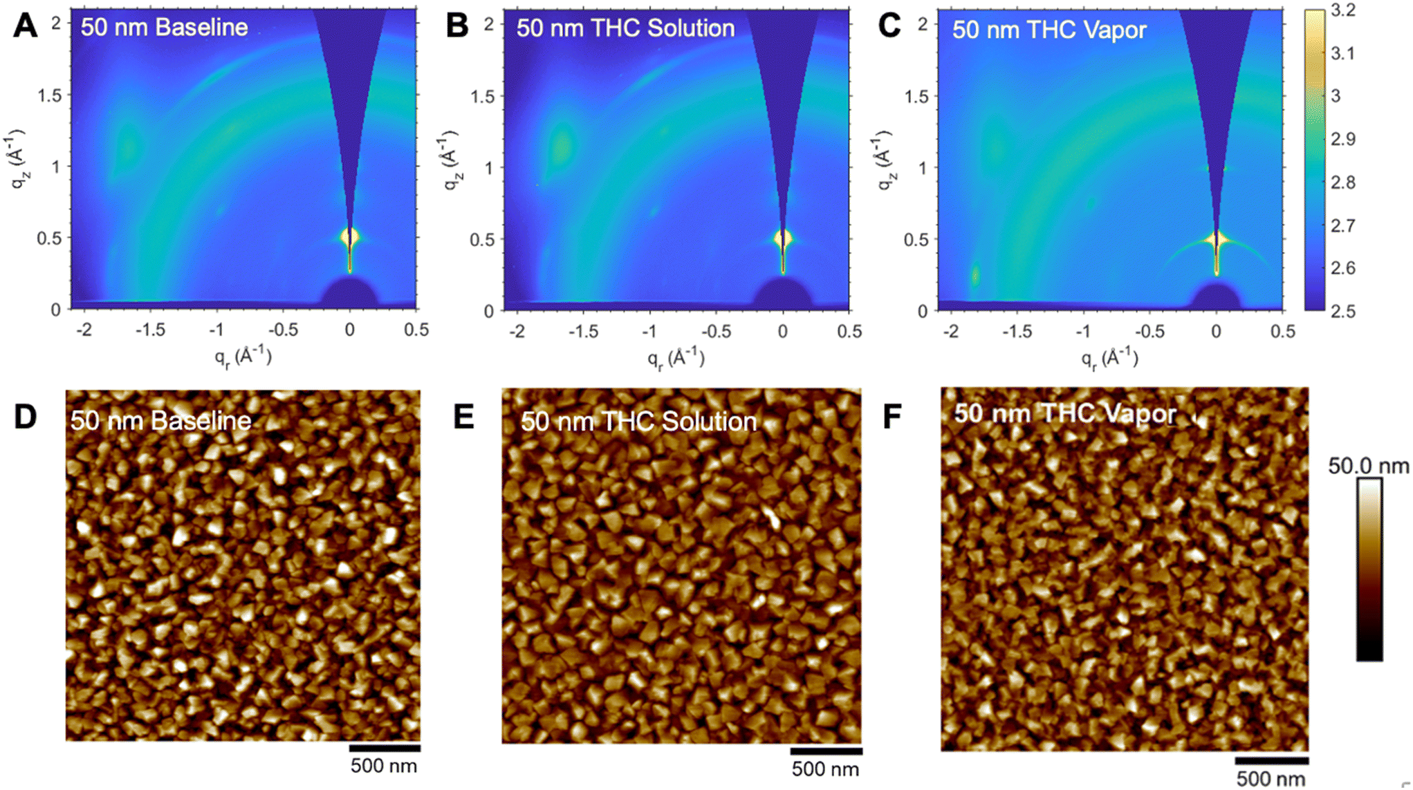 | ||
| Fig. 6 2D scattering patterns (θ = 0.3°) of (A) unexposed baseline, (B) THC solution exposed, and (C) THC vapor exposed 50 nm thick Cl-AlPc. AFM images of (D) unexposed baseline, (E) THC solution exposed, and (F) THC vapor exposed 50 nm thick Cl-AlPc with scale bars of 500 nm. | ||
Notably, small shifts in molecular orientation of the 50 nm films did not produce significant changes in the performance of OTFT sensors. Additionally, the absence of interactions between the 30 nm and 100 nm films and THC by GIWAXS further suggests that the detection mechanism of THC is not purely physical. AFM results demonstrated a slight change in film roughness, more substantial for THC solution, which is accompanied by an increase in detection sensitivity (Fig. 4). The results from the OTFT sensors emphasize that film thickness plays an important role in sensitivity to THC in solution, while W/L imparts a negligible effect in comparison. Jiang et al. demonstrated that sensitivity to NO2 increased with decreasing CuPc film thickness, suggesting that thinner films afford increased analyte interaction with the semiconductive/dielectric interface.32 This has been observed for different semiconductor materials as well.43 As a much larger, pi-conjugated organic molecule, THC is less likely to permeate throughout the film and therefore the process is likely a charge transfer interaction as THC interacts between grain boundaries and the top layer of the Cl-AlPc film. Thinner films facilitate quicker diffusion of charge and as the surface roughness increases, there are more opportunities for the Pc–analyte interaction on the top layer of the film.
For liquid solution THC sensing, the most sensitive devices were those with the most ideal baseline transfer characteristics and most ideal transport of charge through the device. The fastest baseline charge transport did not necessarily result in the most sensitive THC sensors. This effect was less pronounced, but still present for vapor THC sensing. This finding suggests that we should prioritize the reduction of channel and contact resistances during channel architecture design and device fabrication, and the formation of ordered grains in the thin film to produce quality charge transport pathways for high-performing and sensitive THC sensors. Upon exposure to THC, the changes to more ideal transport pathways are more pronounced, especially in thinner films where less transport pathways are available. These results suggest that THC OTFT sensors can be engineered to be more effective for both solution and vapor THC testing, and that the environment or type of THC exposure will lead to different changes in device response.
Conclusion
We optimized Cl-AlPc OTFTs by changing the source-drain electrode configuration (W/L) and the film thickness. We found that increasing the W/L leads to improved mobilities and Ion, but worse transfer curve characteristics. A W/L of 1000 balances the contact and channel resistances to give the best performance with favorable transfer characteristics. It was found to have a limited effect on the sensitivity to THC. An analysis of the different film thicknesses through GIWAXS and AFM showed that the 30 nm films likely had improved charge transport pathways due to higher grain ordering, which led to improved transfer characteristics and sensitivity to THC in solution. The 100 nm films likely had an increased number of charge transport pathways leading to higher mobilities and Ion with disordered grains and worse transfer characteristics, resulting in less sensitive THC sensors. No change in molecular orientation was detected with exposure to THC solution and vapor for the 30 nm and 100 nm films. A slight change was observed for the 50 nm film, but this did not lead to a significant change in performance as an OTFT sensor compared to the other films, indicating that the method of detection of THC and Cl-AlPc is likely not solely dependent on physical changes in the thin film. AFM suggests a slight roughening of the Cl-AlPc film with exposure to THC solution leading to a greater surface area, which could contribute to the overall change in device performance. This study suggests that film thickness plays an important role in the quality of the charge transport pathways in Cl-AlPc OTFTs, which can influence the sensitivity to THC.Experimental section
Materials
Cl-AlPc was obtained from TCI Chemicals and purified by train sublimation before use. (Octyl)trichlorosilane (OTS, 97%) was purchased from TCI Chemicals and used as received. All solvents were HPLC grade and purchased from Fischer Scientific. Cannabinoid standards were obtained from Toronto Research Chemicals.Thin film formation
Prefabricated devices were purchased from Fraunhofer IPMS to make BGBC transistors. Each substrate consisted of a 230 nm thermally grown SiO2 dielectric on a Si gate, with prepatterned gold source-drain electrodes to give five different device architectures: W/L = 100 (W = 2 mm, L = 20 μm), W/L = 200 (W = 2 mm, L = 10 μm), W/L = 400 (W = 2 mm, L = 5 μm), W/L = 800 (W = 2 mm, L = 2.5 μm), and W/L = 1000 (W = 10 mm, L = 10 μm). For AFM and GIWAXS characterization, substrates were purchased from Ossila with 300 nm thermally grown SiO2 dielectric on Si. The substrates were thoroughly washed with acetone to remove the photoresist, then rinsed with isopropanol and dried under a N2 gas stream. The substrates then underwent an oxygen plasma treatment for 15 minutes, after which time they were briefly rinsed with water, isopropanol, and dried again with N2. The substrates were submerged in a 1% v/v OTS solution in toluene at 70 °C for 1 hour. The treated substrates were then rinsed with toluene and isopropanol before being dried with a N2 gas stream and a further drying step in a 70 °C vacuum oven for 1 hour. The substrates were then heated to 140 °C in an Angstrom EvoVac thermal evaporator at a pressure below 2 × 10⁻⁶ Torr and held for 1 hour. Next, Cl-AlPc was deposited onto the surface by sublimation at a rate of 0.2 Å s−1. An in situ servo shutter mask was used to progressively block the plume during fabrication so that all samples were exposed to the same plume at early stages but that some samples were blocked off at early stages and others were blocked when more material could be deposited to form the desired thicknesses of 300 Å, 500 Å, or 1000 Å. After deposition was completed, the substrates were cooled to room temperature before characterization.GIWAXS characterization
GIWAXS experiments were completed at the Canadian Light Source (CLS) in Saskatoon, Canada using the Brockhouse Diffraction Sector (BXDS) beamline with a photon energy of 15.1 keV. A Rayonix MX300 CCD detector (73.242 μm × 73.242 μm pixel size) placed 417 mm from the sample was used to collect 2D scattering patterns at an angle of incidence of θ = 0.3°. Silver behenate and poly(3-hexylthiophene-2,5-diyl) standards were used to calibrate the data, which was analyzed with the GIXSGUI software package in MATLAB, where both polarization and solid-angle corrections were applied.45AFM
AFM measurements (2.5 μm × 2.5 μm) were carried out with a Bruker Dimension Icon AFM equipped with ScanAsyst-Air tips using tapping mode and a scan rate of 0.69 Hz. Image processing and editing was performed with NanoScope Analysis v.1.8 software.OTFT characterization
Transistors with W/L ratios of 100 to 800 were characterized using a custom electrical probe station, oesProbe A10000-P290 (Element instrumentation Inc. & Kreus Design Inc.), and transistors with a W/L ratio of 1000 were tested using a custom-build auto tester apparatus. Both were run using a Keithley 614B SourceMeter and Labview software, where the VSD and VGS were set to discrete values and the ISD was measured. To saturate the devices, six transfer curves were obtained and the final three were averaged to yield the characteristic transfer curve for each transistor, as shown in Fig. S1 and S3.† The VT and Ion/off was determined from these measurements, and the μh was determined using the general expression relating it to the gate voltage in the saturation region, shown again in eqn (1).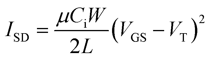 | (1) |
The baseline values for VT, Ion/off and μh were obtained for all devices to assess which semiconductor thickness and channel architecture resulted in the best device performance, and these characteristics were averaged across a minimum of 4 devices for each condition.
Contact resistance was calculated by the M-TLM shown in eqn (2). The total resistance (RT) was obtained from the output curve at a low source-drain voltage. A plot of RTW/L vs. 1/L was generated for the channel lengths of 2.5, 5, 10, and 20 μm. The data was fit with a linear trendline, the slope of which gave the width-normalized contact resistance, RCW.
 | (2) |
Following, the devices were exposed to either to a liquid THC solution or THC vapor. For solution exposure, 0.5 μL of a 20 μM solution of THC in hexanes was drop-cast onto the surface of each transistor channel and allowed to dry for 2 minutes. For vapor exposure, 36 mg of THC was vaporized into an 8 L bag (4.5 mg L−1) using the Vapormed Volcano Medic. The bag was slowly emptied into a small chamber housing the devices where they were exposed to the vapor for a total of 90 seconds. The devices were then characterized again, and new VT, Ion/off and μh values were obtained and compared to the baseline values to assess which devices and channel architectures resulted in the highest sensitivity to THC. The procedure was repeated for CBD solution and CBD vapor.
ANOVA statistical analysis
The two-way ANOVA analysis was performed using the GraphPad Prism software. All Ion and μh values for baseline devices, and all changes in VT, Ion/off and μh for THC-exposed devices were inputted in the software as grouped data. A two-way ANOVA analysis was performed fitting main effects. The Tukey test was used to compare all data pairs individually. The effect of W/L and thickness was reported for the overall data set and all pairs using an α of 0.05 (95% confidence interval), and the results were tabulated.Conflicts of interest
The authors declare no competing financial interests.Acknowledgements
This work was supported by NSERC Discovery grant RGPIN 2015-05796 (A. J. S.), 2015-05453 (C. S. H.), and 2020-04079 (B. H. L.), the Canada Research Chairs Program 950-230754 (A. J. S.) and 950-230724 (B. H. L.). Infrastructure used to complete this work was acquired using CFI-JELF #30488 (B. H. L.) and NSERC RTI 472921-2015 (B. H. L.). We recognize the Centre for Research in Photonics at the University of Ottawa (CRPuO) for allowing access to the AFM. The authors express gratitude to the CLS for granting beamtime, and to Adam Leontowich for his technical support and proficiency during data collection. CLS is supported by CFI, NSERC, the University of Saskatchewan, the Government of Saskatchewan, Western Economic Diversification Canada, the National Research Council Canada, and the Canadian Institutes of Health Research.References
- D. I. Abrams, The Therapeutic Effects of Cannabis and Cannabinoids: An Update from the National Academies of Sciences, Engineering and Medicine Report, Eur. J. Intern. Med., 2018, 49, 7–11, DOI:10.1016/J.EJIM.2018.01.003.
- R. Mechoulam, M. Peters, E. Murillo-Rodriguez and L. O. Hanuš, Cannabidiol – Recent Advances, Chem. Biodiversity, 2007, 4(8), 1678–1692, DOI:10.1002/CBDV.200790147.
- B. De Backer, B. Debrus, P. Lebrun, L. Theunis, N. Dubois, L. Decock, A. Verstraete, P. Hubert and C. Charlier, Innovative Development and Validation of an HPLC/DAD Method for the Qualitative and Quantitative Determination of Major Cannabinoids in Cannabis Plant Material, J. Chromatogr. B: Anal. Technol. Biomed. Life Sci., 2009, 877(32), 4115–4124, DOI:10.1016/j.jchromb.2009.11.004.
- C. Sun, Y. X. Wang, M. Sun, Y. Zou, C. Zhang, S. Cheng and W. Hu, Facile and Cost-Effective Liver Cancer Diagnosis by Water-Gated Organic Field-Effect Transistors, Biosens. Bioelectron., 2020, 164, 112251, DOI:10.1016/J.BIOS.2020.112251.
- C. Sun, R. Li, Y. Song, X. Jiang, C. Zhang, S. Cheng and W. Hu, Ultrasensitive and Reliable Organic Field-Effect Transistor-Based Biosensors in Early Liver Cancer Diagnosis, Anal. Chem., 2021, 93(15), 6188–6194, DOI:10.1021/ACS.ANALCHEM.1C00372/ASSET/IMAGES/LARGE/AC1C00372_0008.JPEG.
- Z. J. Comeau, N. T. Boileau, T. Lee, O. A. Melville, N. A. Rice, Y. Troung, C. S. Harris, B. H. Lessard and A. J. Shuhendler, On-the-Spot Detection and Speciation of Cannabinoids Using Organic Thin-Film Transistors, ACS Sens., 2019, 4, 2706–2715, DOI:10.1021/acssensors.9b01150.
- J. Jo, J. S. Yu, T. M. Lee and D. S. Kim, Fabrication of Printed Organic Thin-Film Transistors Using Roll Printing, Jpn. J. Appl. Phys., 2009, 48(4 PART 2), 04C181, DOI:10.1143/JJAP.48.04C181/XML.
- G. Grau, R. Kitsomboonloha, S. L. Swisher, H. Kang and V. Subramanian, Printed Transistors on Paper: Towards Smart Consumer Product Packaging, Adv. Funct. Mater., 2014, 24(32), 5067–5074, DOI:10.1002/ADFM.201400129.
- J. Kim, T. Hassinen, W. H. Lee and S. Ko, Fully Solution-Processed Organic Thin-Film Transistors by Consecutive Roll-to-Roll Gravure Printing, Org. Electron., 2017, 42, 361–366, DOI:10.1016/J.ORGEL.2016.12.061.
- Z. Lin, X. Guo, L. Zhou, C. Zhang, J. Chang, J. Wu and J. Zhang, Solution-Processed High Performance Organic Thin Film Transistors Enabled by Roll-to-Roll Slot Die Coating Technique, Org. Electron., 2018, 54, 80–88, DOI:10.1016/J.ORGEL.2017.12.030.
- Y. Y. Noh, N. Zhao, M. Caironi and H. Sirringhaus, Downscaling of Self-Aligned, All-Printed Polymer Thin-Film Transistors, Nat. Nanotechnol., 2007, 2(12), 784–789, DOI:10.1038/nnano.2007.365.
- H. Y. Tseng and V. Subramanian, All Inkjet-Printed, Fully Self-Aligned Transistors for Low-Cost Circuit Applications, Org. Electron., 2011, 12(2), 249–256, DOI:10.1016/J.ORGEL.2010.11.013.
- A. De La Fuente Vornbrock, D. Sung, H. Kang, R. Kitsomboonloha and V. Subramanian, Fully Gravure and Ink-Jet Printed High Speed PBTTT Organic Thin Film Transistors, Org. Electron., 2010, 11(12), 2037–2044, DOI:10.1016/J.ORGEL.2010.09.003.
- H. Kang, R. Kitsomboonloha, J. Jang and V. Subramanian, High-Performance Printed Transistors Realized Using Femtoliter Gravure-Printed Sub-10 Mm Metallic Nanoparticle Patterns and Highly Uniform Polymer Dielectric and Semiconductor Layers, Adv. Mater., 2012, 24(22), 3065–3069, DOI:10.1002/ADMA.201200924.
- J. T. Mabeck and G. G. Malliaras, Chemical and Biological Sensors Based on Organic Thin-Film Transistors, Anal. Bioanal. Chem., 2006, 384(2), 343–353, DOI:10.1007/S00216-005-3390-2/FIGURES/8.
- P. Lin, F. Yan, P. Lin and F. Yan, Organic Thin-Film Transistors for Chemical and Biological Sensing, Adv. Mater., 2012, 24(1), 34–51, DOI:10.1002/ADMA.201103334.
- M. Wu, S. Hou, X. Yu and J. Yu, Recent Progress in Chemical Gas Sensors Based on Organic Thin Film Transistors, J. Mater. Chem. C, 2020, 8(39), 13482–13500, 10.1039/D0TC03132A.
- M. E. Roberts, A. N. Sokolov and Z. Bao, Material and Device Considerations for Organic Thin-Film Transistor Sensors, J. Mater. Chem., 2009, 19(21), 3351–3363, 10.1039/B816386C.
- J. Locklin and Z. Bao, Effect of Morphology on Organic Thin Film Transistor Sensors, Anal. Bioanal. Chem., 2006, 384(2), 336–342, DOI:10.1007/S00216-005-0137-Z/FIGURES/6.
- J. N. Arthur, A. K. Pandey, J. M. Nunzi and S. D. Yambem, Insight into OTFT Sensors Using Confocal Fluorescence Microscopy, ACS Appl. Mater. Interfaces, 2022, 14(4), 5709–5720, DOI:10.1021/ACSAMI.1C20143/SUPPL_FILE/AM1C20143_SI_001.PDF.
- O. A. Melville, B. H. Lessard and T. P. Bender, Phthalocyanine-Based Organic Thin-Film Transistors: A Review of Recent Advances, ACS Appl. Mater. Interfaces, 2015, 7(24), 13105–13118, DOI:10.1021/ACSAMI.5B01718.
- D. Elkington, N. Cooling, W. Belcher, P. C. Dastoor and X. Zhou, Organic Thin-Film Transistor (OTFT)-Based Sensors, Electron, 2014, 3(2), 234–254, DOI:10.3390/ELECTRONICS3020234.
- M. Urbani, M. E. Ragoussi, M. K. Nazeeruddin and T. Torres, Phthalocyanines for Dye-Sensitized Solar Cells, Coord. Chem. Rev., 2019, 381, 1–64, DOI:10.1016/J.CCR.2018.10.007.
- G. de la Torre, G. Bottari and T. Torres, Phthalocyanines and Subphthalocyanines: Perfect Partners for Fullerenes and Carbon Nanotubes in Molecular Photovoltaics, Adv. Energy Mater., 2017, 7(10), 1601700, DOI:10.1002/AENM.201601700.
- R. R. Cranston and B. H. Lessard, Metal Phthalocyanines: Thin-Film Formation, Microstructure, and Physical Properties, RSC Adv., 2021, 11(35), 21716–21737, 10.1039/D1RA03853B.
- Z. J. Comeau, N. A. Rice, C. S. Harris, A. J. Shuhendler and B. H. Lessard, Organic Thin-Film Transistors as Cannabinoid Sensors: Effect of Analytes on Phthalocyanine Film Crystallization, Adv. Funct. Mater., 2022, 32(7), 2107138, DOI:10.1002/ADFM.202107138.
- N. T. Boileau, R. Cranston, B. Mirka, O. A. Melville and B. H. Lessard, Metal Phthalocyanine Organic Thin-Film Transistors: Changes in Electrical Performance and Stability in Response to Temperature and Environment, RSC Adv., 2019, 9(37), 21478–21485, 10.1039/C9RA03648B.
- B. H. Lessard, The Rise of Silicon Phthalocyanine: From Organic Photovoltaics to Organic Thin Film Transistors, ACS Appl. Mater. Interfaces, 2021, 13(27), 31321–31330, DOI:10.1021/ACSAMI.1C06060.
- D. Klyamer, A. Sukhikh, S. Gromilov, P. Krasnov and T. Basova, Fluorinated Metal Phthalocyanines: Interplay between Fluorination Degree, Films Orientation, and Ammonia Sensing Properties, Sensors, 2018, 18(7), 2141, DOI:10.3390/S18072141.
- N. T. Boileau, O. A. Melville, B. Mirka, R. Cranston and B. H. Lessard, P and N Type Copper Phthalocyanines as Effective Semiconductors in Organic Thin-Film Transistor Based DNA Biosensors at Elevated Temperatures, RSC Adv., 2019, 9(4), 2133–2142, 10.1039/C8RA08829B.
- Z. J. Comeau, G. A. Facey, C. S. Harris, A. J. Shuhendler and B. H. Lessard, Engineering Cannabinoid Sensors through Solution-Based Screening of Phthalocyanines, ACS Appl. Mater. Interfaces, 2020, 12(45), 50692–50702, DOI:10.1021/acsami.0c17146.
- Y. Jiang, W. Huang, X. Zhuang, Y. Tang and J. Yu, Thickness Modulation on Semiconductor towards High Performance Gas Sensors Based on Organic Thin Film Transistors, Mater. Sci. Eng., B, 2017, 226, 107–113, DOI:10.1016/J.MSEB.2017.08.019.
- A. Demir, S. Bağci, S. E. San and Z. Doğruyol, Pentacene-Based Organic Thin Film Transistor With SiO2 Gate Dielectric, Surf. Rev. Lett., 2015, 22(3) DOI:10.1142/S0218625X15500389.
- R. Ruiz, A. Papadimitratos, A. C. Mayer and G. G. Malliaras, Thickness Dependence of Mobility in pentacene Thin-Film Transistors, Adv. Mater., 2005, 17(14), 1795–1798, DOI:10.1002/ADMA.200402077.
- B. King, O. A. Melville, N. A. Rice, S. Kashani, C. Tonnelé, H. Raboui, S. Swaraj, T. M. Grant, T. McAfee, T. P. Bender, H. Ade, F. Castet, L. Muccioli and B. H. Lessard, Silicon Phthalocyanines for N-Type Organic Thin-Film Transistors: Development of Structure–Property Relationships, ACS Appl. Electron. Mater., 2020, 3(1), 325–336, DOI:10.1021/ACSAELM.0C00871.
- P. Kumar, A. Sharma, S. Yadav and S. Ghosh, Morphology Optimization for Achieving Air Stable and High Performance Organic Field Effect Transistors, Org. Electron., 2013, 14(6), 1663–1672, DOI:10.1016/J.ORGEL.2013.03.027.
- M. Girtan, S. Dabos-Seignon and A. Stanculescu, On Morphological, Structural and Electrical Properties of Vacuum Deposited pentacene Thin Films, Vacuum, 2009, 83(9), 1159–1163, DOI:10.1016/J.VACUUM.2009.03.001.
- H. Jung, J. Whan, H. Hwi, J.-J. Hyo Jung Kim, J. Whan Kim, H. Hwi Lee, B. Lee and J.-J. Kim, GISAXS Studies of Initial Growth Mode and Nanostructure of Bulk Heterojunction Layers in Planar Type Metal Pthanlocyanine, Proc. SPIE, 2012, 8477, 147–149, DOI:10.1117/12.929324.
- P. V. Necliudov, M. S. Shur, D. J. Gundlach and T. N. Jackson, Contact Resistance Extraction in pentacene Thin Film Transistors, Solid-State Electron., 2003, 47(2), 259–262, DOI:10.1016/S0038-1101(02)00204-6.
- H. Klauk, G. Schmid, W. Radlik, W. Weber, L. Zhou, C. D. Sheraw, J. A. Nichols and T. N. Jackson, Contact Resistance in Organic Thin Film Transistors, Solid-State Electron., 2003, 47(2), 297–301, DOI:10.1016/S0038-1101(02)00210-1.
- K. J. Wynne, Crystal and Molecular Structure of Chloro(Phthalocyanina to)Gallium(III), Ga(Pc)Cl, and Chloro(Phthalocyanmato)Aluminum(III), Al(Pc)Cl, Inorg. Chem., 1984, 23(26), 4658–4663, DOI:10.1021/IC00194A048/SUPPL_FILE/IC00194A048_SI_001.PDF.
- B. Nketia-Yawson and Y. Y. Noh, Organic Thin Film Transistor with Conjugated Polymers for Highly Sensitive Gas Sensors, Macromol. Res., 2017, 25(6), 489–495, DOI:10.1007/S13233-017-5108-7.
- T. Xie, G. Xie, H. Du, Y. Zhou, F. Xie, Y. Jiang and H. Tai, The Fabrication and Optimization of Thin-Film Transistors Based on Poly(3-Hexylthiophene) Films for Nitrogen Dioxide Detection, IEEE Sens. J., 2016, 16(7), 1865–1871, DOI:10.1109/JSEN.2015.2480998.
- B. Nketia-Yawson, A. R. Jung, Y. Noh, G. S. Ryu, G. D. Tabi, K. K. Lee, B. Kim and Y. Y. Noh, Highly Sensitive Flexible NH3 Sensors Based on Printed Organic Transistors with Fluorinated Conjugated Polymers, ACS Appl. Mater. Interfaces, 2017, 9(8), 7322–7330, DOI:10.1021/ACSAMI.6B14220/ASSET/IMAGES/LARGE/AM-2016-14220D_0006.JPEG.
- Z. Jiang, GIXSGUI: A MATLAB Toolbox for Grazing-Incidence X-Ray Scattering Data Visualization and Reduction, and Indexing of Buried Three-Dimensional Periodic Nanostructured Films, J. Appl. Crystallogr., 2015, 48(3), 917–926, DOI:10.1107/S1600576715004434.
Footnote |
| † Electronic supplementary information (ESI) available. See DOI: https://doi.org/10.1039/d2sd00071g |
| This journal is © The Royal Society of Chemistry 2022 |