
 Open Access Article
 This Open Access Article is licensed under a Creative Commons Attribution-Non Commercial 3.0 Unported Licence
Revealing the anisotropic phonon behaviours of layered SnS by angle/temperature-dependent Raman spectroscopy†
Xiangnan Gong *a,
Ting Yanb,
Jue Lib,
Jie Liua,
Hanjun Zoua,
Bin Zhanga,
Hong Wu*c,
Zizhen Zhou*b and
Xiaoyuan Zhouab
*a,
Ting Yanb,
Jue Lib,
Jie Liua,
Hanjun Zoua,
Bin Zhanga,
Hong Wu*c,
Zizhen Zhou*b and
Xiaoyuan Zhouab
aAnalytical and Testing Center, Chongqing University, Chongqing 401331, China. E-mail: carefen82082022@163.com
bCollege of Physics, Chongqing University, Chongqing 401331, China. E-mail: zzzhou@cqu.edu.cn
cSchool of Science, Chongqing University of Posts and Telecommunications, Chongqing 400065, China. E-mail: wuhong@cqupt.edu.cn
First published on 10th November 2022
Abstract
Tin sulfide (SnS), a IV–VI group layered compound, has attracted much attention because of its excellent thermoelectric properties along the crystallographic b-axis. However, there are few reports on the identification of its in-plane orientation. We observe a strong anisotropy of the in-plane Raman signal in bulk SnS. With the help of ab initio calculations, the vibrational symmetry of each observed Raman mode in the cleaved (00l)-plane is consistent with the experimental values. The angle-resolved polarized Raman spectroscopy, combined with electron backscattered diffraction technology, is utilized to systematically investigate the in-plane anisotropy of the phonon response and then determine the in-plane orientation. Furthermore, the temperature-dependent and laser-power-dependent Raman scattering analyses reveal that the adjacent layers in the SnS crystals show a relatively weak van der Waals interaction. These findings could provide much-needed experimental information for future applications related to the anisotropic transport properties of SnS single crystals.
Introduction
Orthorhombic tin sulfide (SnS), a binary IV–VI group chalcogenide material consisting of earth-abundant, low-cost and nontoxic elements, has attracted growing attention owing to its various potential applications.1–4 In particular, many works have focused on its thermoelectric applications due to the theoretically predicted excellent thermoelectric performance. SnS exhibits a layered structure with strong Sn–S bonds forming puckered a–b sheets, which stack along the c-axis with weak intermolecular interactions.5 Because of this special crystal structure, its properties usually show strong anisotropy along each axis.1,6 Hence, it is of vital importance to determine the orientation of SnS single crystal, which has a great influence on the properties and the applications in devices. Generally, the X-ray crystal orientation apparatus is used to determine crystal orientation of large-size bulk materials, but cannot deal with the 2D layered materials with in-plane anisotropy.1 The angle-resolved polarized Raman spectroscopy (ARPRS) is anticipated to solve this problem because it is simple, nondestructive, fast and accurate.7,8 Currently, many works have verified the practicability of this method by integrating with angular resolved polarization conductance techniques,8–10 electron microscopy,11,12 optical microscopy,11,12 X-ray diffraction (XRD),13 and quantitative atomic-resolution force image.14 However, to the best of our knowledge, there are few reports focusing on the application of ARPRS along with electron backscattered diffraction (EBSD) technology, which can be used to identify the in-plane direction of the layered single crystals such as SnS in a more macroscopic and simple operation.In this study, high-quality bulk SnS single crystals were successfully synthesized using a modified Bridgman method, the crystal structure was characterized by single crystal X-ray diffractometer (SCXRD) and high-resolution transmission electron microscopy (HRTEM). Besides, a systematic Raman study was implemented on SnS single crystal from both theoretical and experimental perspectives. The observed Raman modes of B13g (49 cm−1), A1g (95 cm−1), B23g (164 cm−1), A2g (192 cm−1), and A3g (218 cm−1) agree with the calculated results by density functional theory (DFT) method. Moreover, the optical anisotropy property of SnS single crystal was systemically investigated by ARPRS technology, in which Raman intensity shows a strong sensitivity to crystal orientation, and its anisotropy is associated with the polarization configurations and photon energies. Combined with EBSD technology, the ARPRS was successfully employed to confirm the in-plane orientation of the SnS single crystal, which would be efficiently to identify the crystal orientation. Finally, temperature-dependent Raman spectroscopy can be used to study the thermal expansion of SnS crystals with anisotropic characteristics. We believe that our findings will provide new insights into the experimental information of layered materials.
Experimental
SnS single crystals were synthesized using the method as previously reported.6 The starting materials of high-purity of Sn granules (99.999%), S powder (99.99%) were weighed intensively according to the stoichiometry of Sn![[thin space (1/6-em)]](https://www.rsc.org/images/entities/char_2009.gif) :S = 1:1 under argon atmosphere. Mixtures were sealed in cone-shaped quartz tubes under a pressure (∼5 × 10⁻⁴ Pa) and encased in another larger quartz tube, evacuated again and flame-sealed. The tubes were heated up to 1273 K over 12 h, and soaked at that temperature for 15 h. SnS single crystals were grown when the furnace cooled to 1100 K at a rate of 1.5 mm h−1 subsequently. Excellent quality of SnS single crystals with diameter of 15 mm and height of 45 mm were grown, as shown in Fig. S1a (ESI†).
:S = 1:1 under argon atmosphere. Mixtures were sealed in cone-shaped quartz tubes under a pressure (∼5 × 10⁻⁴ Pa) and encased in another larger quartz tube, evacuated again and flame-sealed. The tubes were heated up to 1273 K over 12 h, and soaked at that temperature for 15 h. SnS single crystals were grown when the furnace cooled to 1100 K at a rate of 1.5 mm h−1 subsequently. Excellent quality of SnS single crystals with diameter of 15 mm and height of 45 mm were grown, as shown in Fig. S1a (ESI†).
The crystal structure was determined by an Rigaku SuperNova diffractometer (Mo Kα radiation, λ = 0.71073 Å) at room temperature (295 K). The X-ray data collection, intensity data reduction and empirical absorption correction were conducted using CrysAlisPro software. Crystal structures were refined with SHELXL,15 operated using the Olex2 program.16 All atoms were refined anisotropically. The resulting cell parameters, selected atomic coordinates, bond lengths, and bond angles are listed in Tables 1 and S1, S2.† The high angle annular dark field (HAADF), selected area electron diffraction (SAED) and X-ray energy dispersive spectroscopy (EDS) mapping experiments were performed on Thermo Scientific Talos F200S G2 at 200 kV to investigate the microstructure of the samples.
| Empirical formula | SnS |
| Formula weight | 150.75 |
| Temperature | 295(2) K |
| Radiation | Mo Kα |
| Wavelength | 0.71073 Å |
| Crystal system | Orthorhombic |
| Space group | Pnma |
| Unit cell dimensions | a = 11.1935(15) Å |
| b = 3.9833(4) Å | |
| c = 4.3293(5) Å | |
| α = β = γ = 90° | |
| Cell volume | 193.03(4) Å−3 |
| Z | 4 |
| Calculated density | 5.187 g cm−3 |
| Absorption coeeficient | 13.764 mm−1 |
| F(000) | 264.0 |
| Crystal size | 0.15 × 0.12 × 0.09 mm3 |
| Two-theta range for data collection | 7.28° ≤ 2θ ≤ 52.74° |
| Index ranges | −13 ≤ h ≤ 10 |
| −4 ≤ k ≤ 3 | |
| −5 ≤ l ≤ 5 | |
| Reflections collected | 604 |
| Completeness to 100% | θ = 26.37° |
| Absorption correction | Multi-scan |
| Max. and min. transmission | 1.000 and 0.300 |
| Refinement method | Full-matrix least-squares on F2 |
| Independent reflections | 224 [Rint = 0.0273, Rsigma = 0.0334] |
| Data/restraints/parameters | 224/0/13 |
| Goodness-of-fit on F2 | 1.196 |
| Final R indexes [I ≥ 2σ(I)] | R1 = 0.0448, wR2 = 0.1079 |
| Final R indexes [all data] | R1 = 0.0498, wR2 = 0.1135 |
| Largest diff. peak and hole | 2.59 and −1.68 e Å−3 |
EBSD was collected with a NordlysMax2 detector (Oxford Instruments) integrated with a JEOL JSM-7800F FESEM system. The acceleration voltage was 15 kV and the sample tilted at 70°. The crystallographic orientation data was collected using the Aztec EBSD data acquisition software and post-analyzed using the HKL Channel 5 package for crystallographic orientation.
Raman spectra were performed using a HORIBA JobinYvon HR Evolution confocal Raman spectroscopy system with the excitation wavelength of 532 nm and 632.8 nm. High-resolution spectra were collected using a 100× long work distance (NA = 0.9) objective and recorded with 1800 groove mm−1 holographic grating. Based on the backscattering geometry of ARPRS measurements, the polarization direction of the incident laser was fixed to be vertical (along y-axis) by using a polarizer in the beam path; while the parallel and cross configurations were set by the directions of the analyzer along y-axis or x-axis before the spectrometer entrance, corresponding to vertical or horizontal, respectively. The samples were placed on a rotation stage and clockwise rotated around the z-axis by an angle θ between the laser polarization direction and a-axis (zigzag direction) of the crystal coordinates. The schematic diagram of the set-up is shown in Fig. S5 (ESI†). For temperature-dependent Raman measurements, a Janis ST-500 stage was conducted in the temperature range from 77 K to 400 K under 2 × 10⁻⁵ mba. In all cases, a very low incident light power below 0.5 mW was used to avoid any photodegradation of the samples, meanwhile 300 s exposure-time was used to obtain good signal-to-noise ratio spectrums. For laser-power-dependent Raman experiments, the laser power is set by the laser power supply and a set of neutral-density filters together, then the laser power is detected under the objective by the Newport 843-R power-meter with 818-UV head. All spectra had been calibrated by mercury peak at 546.07 nm for 532 nm laser excitation, and neon peaks at 640.22 nm and 638.29 nm for 632.8 nm laser excitation, respectively.
First principles calculation based on density functional theory (DFT) and augmented plane wave (PAW) method was performed in the Vienna Ab initio Simulation Package (VASP).17–19 The exchange-correlation functional was defined by a generalized gradient approximation (GGA) of Perdew–Burke–Ernzerhof (PBE).20 The convergence of the total energies was set to be 1 × 10⁻⁸ eV. The geometry was fully relaxed until the forces on the atoms were less than 1 × 10⁻⁴ eV Å−1 with an energy cutoff 500 eV. For the Brillouin zone integrations, the Monkhorst–Pack (MP) K-points scheme of 3 × 9 × 9 was adopted. The phonon spectrum of SnS was calculated using the frozen phonon method using a 2 × 2 × 2 supercell, which is implemented in the Phonopy package.21
Results and discussion
Tin sulfide crystallizes in an orthorhombic space group Pnma (No. 62) along the [100] direction, with the lattice parameters of a = 11.1935(15) Å, b = 3.9833(4) Å, c = 4.3293(5) Å, and α = β = γ = 90°, which is verified by SCXRD as shown in Fig. 1a. Details of the diffraction data and crystal structure refinement are summarized in Table 1. Each Sn atom is coordinated by six S atoms in a highly distorted octahedral geometry. Owing to this strong distortions, Sn atom is displaced toward one of the faces of the octahedra, it leads to three short Sn–S bonds of ∼2.626 Å and three long Sn–S bonds of ∼2.664 Å, being responsible for the strong lattice anharmonicity.22 There are two SnS layers in a unit cell and one of the long Sn–S bond resides on the neighboring layer interacted by the weak van der Waals forces, as displayed in Fig. S1a and Table S1 (ESI†). Fig. 1b and c display the HAADF image and corresponding SAED pattern indexed to the zone of [100], respectively. Based on the HAADF image, the d-spacing of interplanar planes was measured as ∼2.932 Å of both (011) and (0![[1 with combining macron]](https://www.rsc.org/images/entities/char_0031_0304.gif) 1). Additionally, the clear Bragg spots of [100] SAED pattern without the appearance of any extra spots indicate the single crystal of as-synthesized SnS samples. The elements were evenly distributed and further confirmed by the direct evidence of STEM-EDS mappings, as depicted in Fig. 1d. Furthermore, XRD experiment was carried out to identify the crystal structure of as-grown samples. As shown in Fig. S2a (ESI†), two main XRD peaks belong to the (400) and (800) planes obtained on the (100) cleavage surface. Additionally, we collected powder XRD patterns of as-grown samples in Fig. S2b (ESI†) for phase identification. All major diffraction peaks can be indexed to the orthorhombic structure (PDF#01-073-1859) with the space group of Pnma, indicating no secondary phases.
1). Additionally, the clear Bragg spots of [100] SAED pattern without the appearance of any extra spots indicate the single crystal of as-synthesized SnS samples. The elements were evenly distributed and further confirmed by the direct evidence of STEM-EDS mappings, as depicted in Fig. 1d. Furthermore, XRD experiment was carried out to identify the crystal structure of as-grown samples. As shown in Fig. S2a (ESI†), two main XRD peaks belong to the (400) and (800) planes obtained on the (100) cleavage surface. Additionally, we collected powder XRD patterns of as-grown samples in Fig. S2b (ESI†) for phase identification. All major diffraction peaks can be indexed to the orthorhombic structure (PDF#01-073-1859) with the space group of Pnma, indicating no secondary phases.
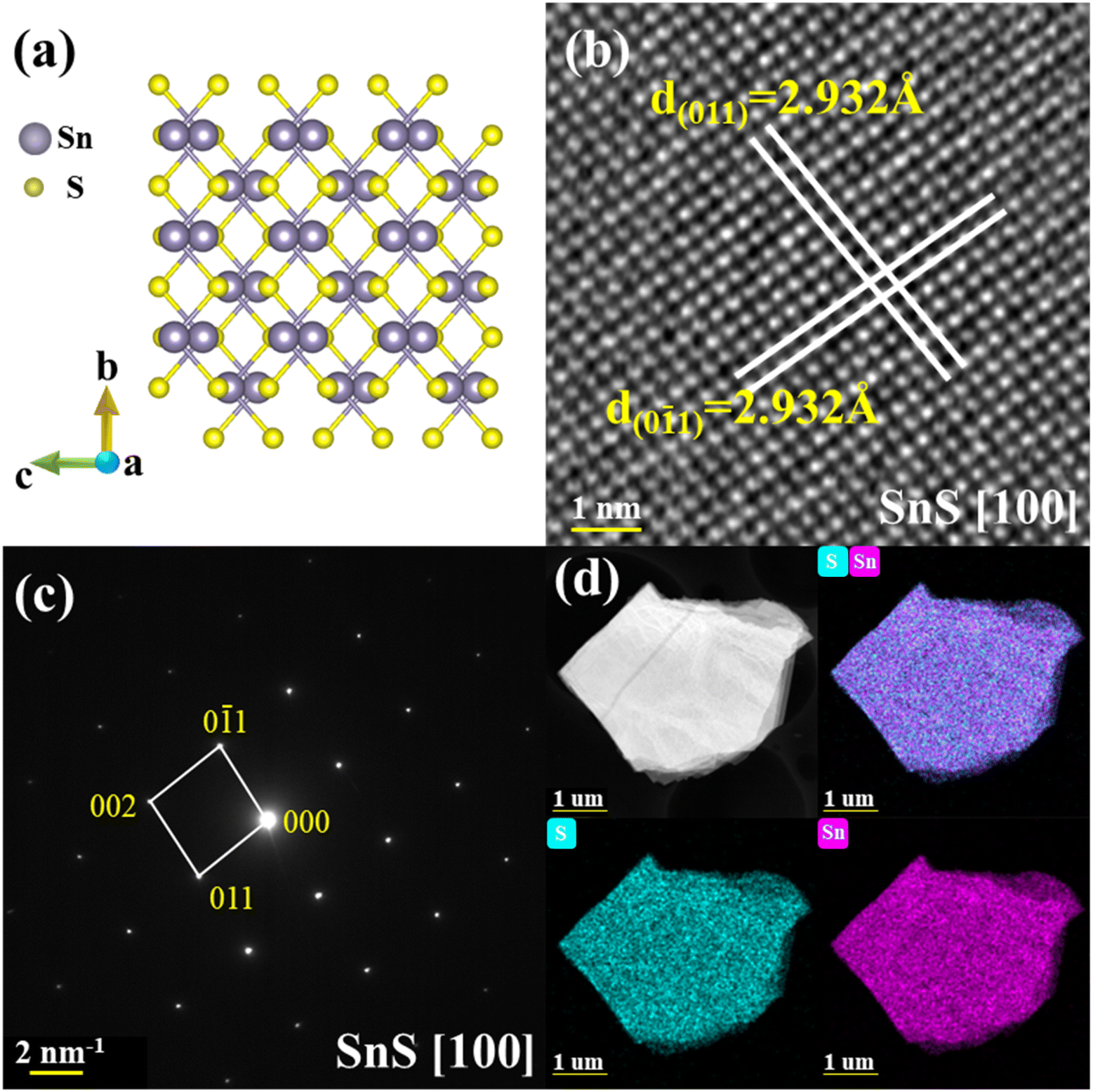 | ||
| Fig. 1 .Structural characterization of SnS single crystal along the [100] direction. (a) The atomic arrangement of SnS (Pnma). (b) The HAADF image. (c) The SAED pattern. (d) STEM-EDS mapping. | ||
A unit cell of SnS contains 8 atoms, which leads to theoretically 24 vibrational modes in the phonon dispersions. The crystal symmetry determined irreducible representation of D2h at the center of the Brillouin zone (Γ point) is represented as:23,24
| Γ = 4Ag + 2B1g + 4B2g + 2B3g + 2Au + 4B1u + 2B2u + 4B3u |
Also, the phonon dispersions calculated by the DFT method are shown in the left side of Fig. 2a, in which the 24 simulated curves are displayed as consistent with those previously reported.25 Three colored curves at the bottom represent the acoustic phonon vibrations including two transverse acoustic phonons (TA and TA′) and one longitudinal acoustic phonon (LA), while the other 21 vibration modes belong to the optical branch. Among them, 5 Raman active modes, B13g, A1g, B23g, A2g, and A3g are specially marked as red squares at gamma (Γ) point and corresponding Raman modes have been carried out based on our back-scattering geometry configuration and the cleavage (100) plane, located at 49, 95, 164, 192 and 218 cm−1 at room temperature, respectively. The corresponding molecular vibration is exhibited in Fig. 2b. In addition, the phonon density of states (DOS) of SnS crystal was displayed on the right side of Fig. 2a, which clearly shows that the phonon DOS below 150 cm−1 mainly contributed by the heavier Sn atom (green line), whereas the DOS above 150 cm−1 primarily results from the S element with lighter atomic mass (red line). As previously reported, many materials with low-symmetric structures exhibit anisotropic transport properties, including the phonon vibrational properties.24,26–28 Raman spectroscopy could provide fruitful information about crystal structures and phonon properties. We carried out ARPRS experiments on SnS single crystals to study its phonon vibrational anisotropy based on the backscattering geometry. The incident laser polarization (ei) was kept along the horizontal direction (x-direction as denoted in Fig. S1a†), while the scattered Raman signals polarization (es) was parallel or perpendicular to the incident laser polarization by using a linear analyzer before the spectrometer entrance slit. Fig. 3a depicts the Raman spectra of SnS measured at an angle 0° under three kinds of polarized configurations including unpolarized, parallel and perpendicular. Five Raman peaks can be detected in unpolarized configuration and assigned as Ag and B3g modes, but the intensity of some Raman peaks varies in parallel and perpendicular configurations, showing the polarization property. Fig. 3b and c present the false-color plots of parallel and perpendicular polarized Raman intensities with the rotation angle ranging from 0° to 360°, respectively. It is observed that B3g modes exhibit a 4-folded shape (e.g., 49 and 164 cm−1) and Ag modes yield a 2-folded shape (e.g., 95 and 192 cm−1) under both parallel and perpendicular polarization configurations. Compared to the two false-color maps, the relative intensity of B13g mode is strongest in parallel polarization configurations, while the A1g mode is the strongest in perpendicular polarization configurations. These two modes can be used to analysis the angle orientation. It should be noted that B13g mode is almost disappearing in perpendicular polarization configurations and can still hold the 4-folded shape. The ARPRS experiment of SnS crystal was also excited under 632.8 nm laser, as shown in Fig. S3 (ESI†). These results clearly reveal that the polarized Raman spectra are strongly dependent on crystalline orientation. To provide preliminary insight into the phenomenon, the intensity I of Raman peaks can be expressed as:29
| I ∝ |ei × R × eTs|2 |
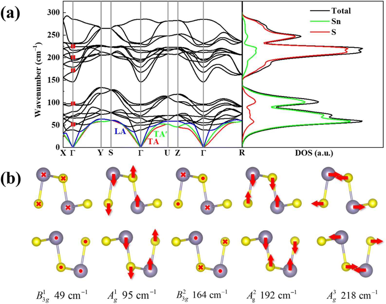 | ||
| Fig. 2 .(a) Phonon dispersion curves of SnS calculated by DFT method for the cleavage plane. Five detected Raman modes are marked as red squares at Γ point. (b) Side views of the atomic vibrations of the 5 Raman active modes measured in the range of 40–300 cm−1. Two adjacent layers of SnS are represented as two rows in the figures. | ||
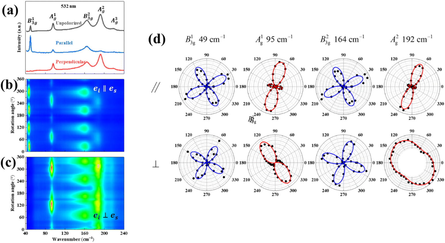 | ||
| Fig. 3 .ARPRS of SnS single crystal on the cleavage plane excited by 532 nm. (a) Measuring Raman spectra at a 0° angle under unpolarized, parallel and perpendicular configurations. False-colour plots of polarized Raman intensities under (b) parallel and (c) perpendicular polarization configurations, respectively. (d) The corresponding ARPRS intensities in parallel and perpendicular polarization configurations (the red and blue lines represent B3g and Ag modes, respectively). | ||
The Raman tensor R can be found in the table of point group D2h:
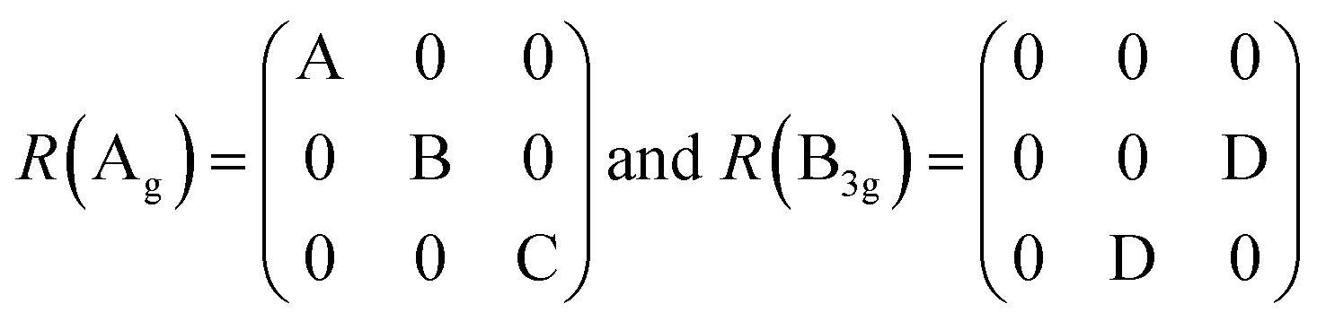
The polarization vector for incident light is ei = (0cosθsinθ). The es = (0cosθsinθ) or es = (0−sinθcosθ) under parallel or perpendicular polarization configuration for scattered light, respectively, where θ is the angle between the incident laser polarization and x-direction of the SnS crystal. The intensities for each mode can be calculated as follows:
| I(Ag, ∥) ∝ (Bcos2θ + Csin2θ) |
| I(B3g, ∥) ∝ D2sin22θ |
| I(B3g, ⊥) ∝ D2cos22θ |
In order to effectively utilize ARPRS technology to identify the in-plane orientation of SnS crystal, we also confirm crystal orientation by EBSD technology, because it can be used to determine the orientation of small grains in nano films.30–34 Fig. 4a shows the inverse pole figures (IPF) coloring of each axis, and the chromaticity coordinates are along z-axis (100-direction), suggesting a high degree of orientation and large size of the crystal with no grain boundary in sight.32 As can be estimated from the pole figures (PF) in Fig. 4b, the distribution of the direction is mainly parallel to {100} but tilt an angle ∼14.9° (ref. 35), which can be seen clearly from {010} direction. The folded IPF in Fig. 4c also shows an orientation tilt ∼14.9°. These EBSD results confirm that the ARPRS technology is a fast, accurate, and non-destructive directional technology to identify the in-plane orientation of the SnS crystal.
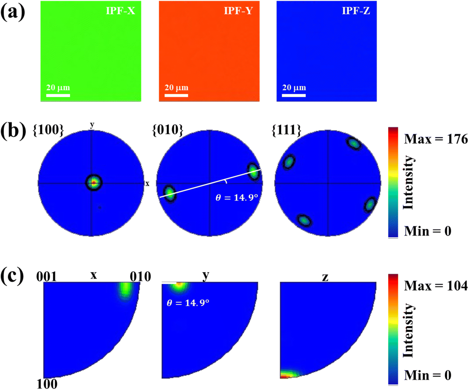 | ||
| Fig. 4 .EBSD pole figure analysis from the in-plane center region of the SnS single crystal. (a) IPF maps from each axis in the center region of sample. (b) Pole figures and (c) folded pole figures. | ||
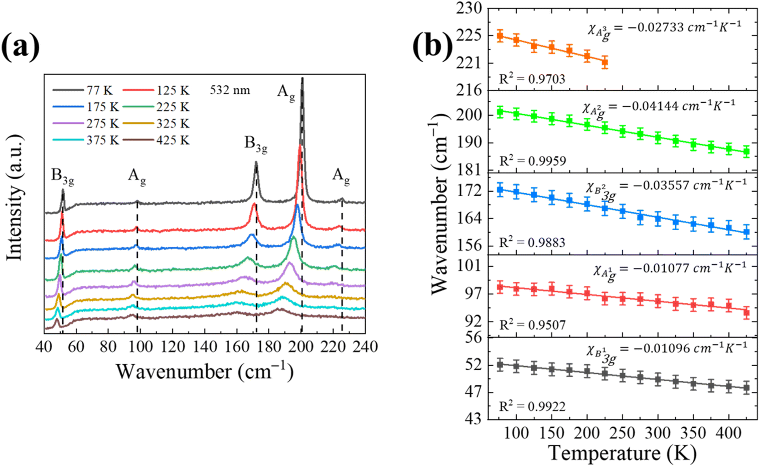
Furthermore, temperature-dependent Raman spectroscopy is a useful method to study the thermal expansion and thermal conductivity properties of the anisotropic SnS bulk.36 Firstly, the laser-power dependent Raman spectroscopy results in Fig. S4† were carried out to show that lower incident laser power should be used to avoid any additional thermal effects. Then we systematically investigated the temperature-dependent Raman behavior of SnS by Nd:YAG excitation laser (532 nm), as shown in Fig. 5 at the temperature range from 77 to 425 K in a vacuum chamber.
 | ||
| Fig. 5 .(a) In situ Raman spectra of SnS single crystal excited by 532 nm from 77 to 425 K on the cleavage plane. (b) Temperature dependence of the Raman peak positions and the corresponding fit (solid lines). | ||
Fig. 5a show that all B3g and Ag Raman modes red-shift and the full width at half maximum (FWHM) of those modes increases with the rising temperature. The measured temperature dependence of the Raman mode frequency shift in the SnS can be characterized by a linear equation:
| ω = ω0 + χT |
| Materials | λlaser (nm) | Raman modes | χ (cm−1 K−1) | Ref. |
|---|---|---|---|---|
| Single-layer graphene | 488 | G band | −0.016 | 38 |
| Bi-layer graphene | G band | −0.015 | ||
| Monolayer MoS2 | 514.5 | E12g | −0.011 | 39 |
| A1g | −0.013 | |||
| Few-layer MoS2 | 532 | E12g | −0.0132 | 40 |
| Monolayer WS2 | 532 | A1g | −0.0149 | 41 |
| E12g | −0.0125 | |||
| Bilayer WS2 | A1g | −0.0121 | ||
| E12g | −0.0133 | |||
| Single-layer MoSe2 | 514.5 | A1g | −0.0054 | 42 |
| A22u | −0.0086 | |||
| Three-layer MoSe2 | A1g | −0.0045 | ||
| A22u | −0.0085 | |||
| SnSe single crystal | 532 | B3g | −0.041 | 36 |
| A2g | −0.043 | |||
| A3g | −0.014 | |||
| SnS single crystal | 532 | B3g | −0.011 | This work |
| A1g | −0.011 | |||
| B3g | −0.036 | |||
| A2g | −0.041 | |||
| A3g | −0.027 |
Conclusions
In conclusion, we observed the strong anisotropy of SnS single crystal through ARPRS technology. The results were fitted and matched well with the classical Raman scattering theory, which showed different periodic properties depending on the excitation wavelengths and polarization configurations. The ARPRS along with EBSD technologies in the present study provide very useful information to quickly determine the in-plane crystallographic orientations of SnS and further improve the accuracy. The temperature coefficients from Raman can be used to distinguish the in-plane and out-of-plane modes. All obtained results can be applied for further analysis of SnS and other van der Waals layered materials for real devices in the future.Author contributions
X. G. conceived the idea and discussed with T. Y., J. L., C. Y., J. L. H. Z., B. Z., H. W., Z. Z. and X. Z.; X. G. performed characterizations, analysed all data. T. Y. and J. L. carried out polarized Raman measurements and analysed the data. H. W. performed materials synthesis, DFT calculation. J. L. and B. Z. performed the HRTEM measurement and analysed the data. H. Z. performed the XRD measurement and analysed the data. X. G. wrote the preliminary draft and revised the manuscript. X. G., H. W., Z. Z., and X. Z. discussed the results and revised the manuscript. All authors contributed to interpreting the findings, reviewing, and commenting on the manuscript.Conflicts of interest
There are no conflicts to declare.Acknowledgements
This work was financially supported by large instrument and equipment function development project of Chongqing University (gnkf2022021), the 16th National Undergraduate Innovation and Entrepreneurship Training Program (202210611098), the 6th Undergraduate Innovation and Entrepreneurship Training Program of Chongqing (S202110611454). and the National Natural Science Foundation of China (Grant No. 12204080). We would like to thank Mr Rui Hong at College of Materials Science and Engineering in Chongqing University for his help in EBSD measurement.Notes and references
- W. He, D. Wang, H. Wu, Y. Xiao, Y. Zhang, D. He, Y. Feng, Y. J. Hao, J. F. Dong, R. Chetty, L. Hao, D. Chen, J. Qin, Q. Yang, X. Li, J. M. Song, Y. Zhu, W. Xu, C. Niu, X. Li, G. Wang, C. Liu, M. Ohta, S. J. Pennycook, J. He, J. F. Li and L. D. Zhao, Science, 2019, 365, 1418–1424 CrossRef CAS PubMed.
- K. Liang, L. Ju, S. Koul, A. Kushima and Y. Yang, Adv. Energy Mater., 2019, 9, 1802543 CrossRef.
- H. Tian, C. Fan, G. Liu, S. Yuan, Y. Zhang, M. Wang and E. Li, Appl. Surf. Sci., 2019, 487, 1043–1048 CrossRef CAS.
- L. A. Burton, D. Colombara, R. D. Abellon, F. C. Grozema, L. M. Peter, T. J. Savenije, G. Dennler and A. Walsh, Chem. Mater., 2013, 25, 4908–4916 CrossRef CAS.
- J. R. Brent, D. J. Lewis, T. Lorenz, E. A. Lewis, N. Savjani, S. J. Haigh, G. Seifert, B. Derby and P. O'Brien, J. Am. Chem. Soc., 2015, 137, 12689–12696 CrossRef CAS PubMed.
- H. Wu, X. Lu, G. Y. Wang, K. L. Peng, H. Chi, B. Zhang, Y. J. Chen, C. J. Li, Y. C. Yan, L. J. Guo, C. Uher, X. Y. Zhou and X. D. Han, Adv. Energy Mater., 2018, 8, 1800087 CrossRef.
- X.-L. Liu, X. Zhang, M.-L. Lin and P.-H. Tan, Chin. Phys. B, 2017, 26, 067802 CrossRef.
- J. Wu, N. Mao, L. Xie, H. Xu and J. Zhang, Angew. Chem., Int. Ed., 2015, 54, 2366–2369 CrossRef CAS PubMed.
- X. Xu, Q. Song, H. Wang, P. Li, K. Zhang, Y. Wang, K. Yuan, Z. Yang, Y. Ye and L. Dai, ACS Appl. Mater. Interfaces, 2017, 9, 12601–12607 CrossRef CAS PubMed.
- L. Li, P. Gong, W. Wang, B. Deng, L. Pi, J. Yu, X. Zhou, X. Shi, H. Li and T. Zhai, ACS Nano, 2017, 11, 10264–10272 CrossRef CAS PubMed.
- J. Kim, J. U. Lee, J. Lee, H. J. Park, Z. Lee, C. Lee and H. Cheong, Nanoscale, 2015, 7, 18708–18715 RSC.
- J. Lee, T. Y. Ko, J. H. Kim, H. Bark, B. Kang, S. G. Jung, T. Park, Z. Lee, S. Ryu and C. Lee, ACS Nano, 2017, 11, 10935–10944 CrossRef CAS PubMed.
- N. Fleck, T. D. C. Hobson, C. N. Savory, J. Buckeridge, T. D. Veal, M. R. Correia, D. O. Scanlon, K. Durose and F. Jäckel, J. Mater. Chem. A, 2020, 8, 8337–8344 RSC.
- Q. Song, X. Pan, H. Wang, K. Zhang, Q. Tan, P. Li, Y. Wan, Y. Wang, X. Xu, M. Lin, X. Wan, F. Song and L. Dai, Sci. Rep., 2016, 6, 29254 CrossRef PubMed.
- G. M. Sheldrick, Acta Crystallogr., Sect. C: Struct. Chem., 2015, 71, 3–8 Search PubMed.
- O. V. Dolomanov, L. J. Bourhis, R. J. Gildea, J. A. K. Howard and H. Puschmann, J. Appl. Crystallogr., 2009, 42, 339–341 CrossRef CAS.
- G. Kresse and J. Furthmuller, Phys. Rev. B: Condens. Matter Mater. Phys., 1996, 54, 11169–11186 CrossRef CAS PubMed.
- G. Kresse and D. Joubert, Phys. Rev. B: Condens. Matter Mater. Phys., 1999, 59, 1758–1775 CrossRef CAS.
- P. E. Blochl, Phys. Rev. B: Condens. Matter Mater. Phys., 1994, 50, 17953–17979 CrossRef PubMed.
- J. P. Perdew, K. Burke and M. Ernzerhof, Phys. Rev. Lett., 1996, 77, 3865–3868 CrossRef CAS PubMed.
- A. Togo and I. Tanaka, Scr. Mater., 2015, 108, 1–5 CrossRef CAS.
- L. Xu, W. Wang, Q. Xie, C. Hu, L. Chen, J. Zheng, H. Yin, G. Cheng and X. Ai, J. Raman Spectrosc., 2021, 53, 104–112 CrossRef.
- H. R. Chandrasekhar, R. G. Humphreys, U. Zwick and M. Cardona, Phys. Rev. B: Solid State, 1977, 15, 2177–2183 CrossRef CAS.
- X. Zhang, Q. H. Tan, J. B. Wu, W. Shi and P. H. Tan, Nanoscale, 2016, 8, 6435–6450 RSC.
- R. Guo, X. Wang, Y. Kuang and B. Huang, Phys. Rev. B: Condens. Matter Mater. Phys., 2015, 92, 115202 CrossRef.
- D. Yoon, Y. W. Son and H. Cheong, Phys. Rev. Lett., 2011, 106, 155502 CrossRef PubMed.
- H. Liu, A. T. Neal, Z. Zhu, Z. Luo, X. Xu, D. Tomanek and P. D. Ye, ACS Nano, 2014, 8, 4033–4041 CrossRef CAS PubMed.
- F. Xia, H. Wang and Y. Jia, Nat. Commun., 2014, 5, 4458 CrossRef CAS PubMed.
- R. Loudon, Adv. Phys., 2001, 50, 813–864 CrossRef.
- M. M. Nowell, M. A. Scarpulla, N. R. Paudel, K. A. Wieland, A. D. Compaan and X. Liu, Microsc. Microanal., 2015, 21, 927–935 CrossRef CAS PubMed.
- J. Kamimura, M. Ramsteiner, U. Jahn, C.-Y. James Lu, A. Kikuchi, K. Kishino and H. Riechert, J. Phys. D: Appl. Phys., 2016, 49, 155106 CrossRef.
- A. Winkelmann, G. Cios, T. Tokarski, G. Nolze, R. Hielscher and T. Kozieł, Acta Mater., 2020, 188, 376–385 CrossRef CAS.
- N. Schafer, A. J. Wilkinson, T. Schmid, A. Winkelmann, G. A. Chahine, T. U. Schulli, T. Rissom, J. Marquardt, S. Schorr and D. Abou-Ras, Ultramicroscopy, 2016, 169, 89–97 CrossRef PubMed.
- T. Schmid, N. Schafer, S. Levcenko, T. Rissom and D. Abou-Ras, Sci. Rep., 2015, 5, 18410 CrossRef CAS PubMed.
- L. D. Zhao, S. H. Lo, Y. Zhang, H. Sun, G. Tan, C. Uher, C. Wolverton, V. P. Dravid and M. G. Kanatzidis, Nature, 2014, 508, 373–377 CrossRef CAS PubMed.
- X. Gong, H. Wu, D. Yang, B. Zhang, K. Peng, H. Zou, L. Guo, X. Lu, Y. Chai, G. Wang and X. Zhou, Vib. Spectrosc., 2020, 107, 103034 CrossRef CAS.
- M. Dutta, D. Sarkar and K. Biswas, Chem. Commun., 2021, 57, 4751–4767 RSC.
- I. Calizo, A. A. Balandin, W. Bao, F. Miao and C. N. Lau, Nano Lett., 2007, 7, 2645–2649 CrossRef CAS PubMed.
- R. Yan, J. R. Simpson, S. Bertolazzi, J. Brivio, M. Watson, X. Wu, A. Kis, T. Luo, A. R. Hight Walker and H. G. Xing, ACS Nano, 2014, 8, 986–993 CrossRef CAS PubMed.
- S. Sahoo, A. P. S. Gaur, M. Ahmadi, M. J. F. Guinel and R. S. Katiyar, J. Phys. Chem. C, 2013, 117, 9042–9047 CrossRef CAS.
- N. Peimyoo, J. Shang, W. Yang, Y. Wang, C. Cong and T. Yu, Nano Res., 2014, 8, 1210–1221 CrossRef.
- D. J. Late, S. N. Shirodkar, U. V. Waghmare, V. P. Dravid and C. N. Rao, ChemPhysChem, 2014, 15, 1592–1598 CrossRef CAS PubMed.
Footnote |
| † Electronic supplementary information (ESI) available. See DOI: https://doi.org/10.1039/d2ra06470g |
| This journal is © The Royal Society of Chemistry 2022 |