DOI:
10.1039/D2RA04964C
(Paper)
RSC Adv., 2022,
12, 31518-31524
First-principles investigation of potential water-splitting photocatalysts and photovoltaic materials based on Janus transition-metal dichalcogenide/WSe2 heterostructures
Received
8th August 2022
, Accepted 26th October 2022
First published on 3rd November 2022
Abstract
Two-dimensional materials have been shown to exhibit exotic properties that make them very interesting for both photo-catalytic and photo-voltaic applications. In this study, van der Waals corrected density functional theory calculations were carried out on heterostructures of MoSSe/WSe2, WSSe/WSe2, and WSeTe/WSe2. The heterostructures are semiconductors with type II band alignments which are advantageous for electron–hole pair separation. The HSE06 level electronic band gap was found to be 1.093 eV, 1.427 eV and 1.603 eV for MoSSe/WSe2, WSSe/WSe2, and WSeTe/WSe2 respectively. We have considered eight high symmetry stacking patterns for each of the heterostructures, and among them the most stable stacking orders were ascertained based on the interlayer binding energies. The binding energies of the most stable MoSSe/WSe2, WSSe/WSe2, and WSeTe/WSe2 heterostructures were found to be −0.0604 eV, −0.1721 eV, and −0.3296 eV with an equilibrium interlayer space of 5.75 Å, 4.05 Å, and 4.76 Å respectively. The Power Conversion Efficiency (PCE) was found to be 20, 19.98, and 18.24 percent for the MoSSe/WSe2, WSSe/WSe2, and WSeTe/WSe2 heterostructures, respectively. The results show that they can serve as suitable photovoltaic materials with high efficiency, thus, opening the possibilities of developing solar cells based on 2D Janus/TMD heterostructures. The most stable heterostructures are also tested for photocatalytic water splitting applications and WSeTe/WSe2 shows excellent photocatalytic activity by being active for full water splitting at pH = 7 and pH = 14, the MoSSe/WSe2 heterostructure is good for the oxygen evolution reaction and WSSe/WSe2 is active for the hydrogen evolution reaction.
1 Introduction
Since graphene was isolated from highly oriented pyrolytic graphite (HOPG) for the first time in 2004,1 graphene’s success has stimulated an explosive interest in other 2D materials, where using different elements opens up new possibilities for exciting new physics and ultimately thin devices.2 To synthesize 2D materials, a variety of chemical and physical methods, such as mechanical exfoliation, chemical exfoliation of bulk structures, chemical vapor deposition (CVD) of thin films, and so on, can be used.3,4 There are various kinds of two-dimensional (2D) materials.5–12 Some of the most common 2D materials are transition metal dichalcogenides (TMDs), whose chemical composition is usually represented by MX2, and whose structure consists of one transition metal (M) atom layer sandwiched between two chalcogen (X) atom layers.13–15 MX2 monolayers have a direct band gap between 1.0 and 1.9 eV,16,17 excellent carrier mobility, and a strong spin–orbit coupling (SOC) effect due to the d orbitals of the heavy metal atom.18 Among the TMDs of group-VIB, WSe2 has emerged as a material with many outstanding properties,19,20 and the first exfoliation occurred in 2013.21–23 Bulk WSe2 was used previously in photovoltaic cells24,25 and for photoelectrochemical (PEC) hydrogen production26 because of its suitable band gap and long-term stability. Also with layer-by-layer stacking, WSe2 demonstrates newly explored properties after being encapsulated with atomically thin materials, or incorporated in van der Waals heterostructures.27–29
The successful experimental synthesis of the MoSSe compound in 2014 added a new member to the TMD family, which is known as Janus MXY (M = Mo, W; X, Y = S, Se).30 Due to the different atomic species on each side of the metal layer, they exhibit a high dipole across the plane. The Janus monolayer is composed of three atomic layers stacked in the X–M–Y sequence. The spin–orbit coupling and the band structures of the Janus MXY monolayers, like their parent TMD structure, display stable spin splitting at the band margins near the K point.31 When the Janus MXY (JTMD) comes into contact with other materials on different sides, it can form unique structures with a variety of properties.32 JTMD monolayers have moderate band gaps between 1.37 and 1.96 eV,33 pronounced visible-light absorption, and a carrier mobility ranging from 28 to 606 cm2 V−1 s−1 with type-II band alignment present in most cases. Type-II band alignment forms in JTMD bilayers with significantly large band offset, which is beneficial for exciton lifetimes and thus more appealing in light-energy conversion.30 This observation makes JTMD monolayers promising candidates for electronics, photovoltaics, and photocatalysis.34 MoSSe’s mirror asymmetry reveals an intrinsic out-of-plane electric field.35,36 Also, MoSSe has been shown to possess an enhanced Rashba effect and a high exciton binding energy,37,38 and it is also an excellent photocatalyst for solar water decomposition.35,39–41 MoSSe’s unique properties have opened up new avenues for application.30 The small effective mass of MoSSe leads to higher carrier mobility, which is highly desirable for high performance device applications.42 WSSe and WSeTe have higher carrier mobilities due to their small effective masses and large elastic constants. Compared with conventional TMD monolayers such as MoS2 (60 ∼ 200 cm2 V−1 s−1),43,44 WSSe and WSeTe exhibit higher carrier mobilities. Recently, Janus TMD structures have been widely investigated, following the growth of a MoSSe monolayer using a synthetic strategy with vertical dipoles.45 Combining polarized Janus MXY monolayers to form bilayer structures or with other 2D layers to form vdW heterostructures results in new properties.30
The weak vdW forces between two different layered materials result in an energetically stable heterostructure.46,47 The interface of a 2D heterostructure results in various interesting properties, which enhance the electronic, optical, and photocatalytic abilities.8,48,49 As a result, a variety of 2D heterostructure materials have been developed and used as p–n junctions,50 photocatalysts,51 photovoltaic devices, field-effect transistors,52 biosensors, light emitting diodes, light detectors, and energy storage devices.53 In this study, first-principles calculations were performed based on DFT to investigate the electronic, photocatalytic, and photovoltaic properties of MoSSe/WSe2, WSSe/WSe2, and WSeTe/WSe2 vdW heterostructures. Eight different heterostructure configurations were considered, and the structures with minimum binding energy were selected for further analysis. The electronic properties of MoSSe–WSe2, WSSe–WSe2, and WSeTe–WSe2 vdW heterostructures were evaluated and we observed that they are all semiconducting. The results show that the vdW heterostructures exhibit type II band alignment, which is an excellent property for efficiently separating excitons, good for photovoltaics and photocatalytic water splitting. The Power Conversion Efficiency (PCE) was found to be 20 percent, 19.98 percent, and 18.24 percent for the MoSSe/WSe2, WSSe/WSe2, and WSeTe/WSe2 heterostructures, respectively, which makes them good candidates for photovoltaic solar cells. WSeTe/WSe2 shows excellent photocatalytic activity by being active for full water splitting under basic and acidic conditions, the MoSSe/WSe2 heterostructure is good for the oxygen evolution reaction and WSSe/WSe2 is active for the hydrogen evolution reaction. In general, we were the first to study these heterostructures, and the systems performed well in photovoltaic and water splitting applications. The heterobilayers presented in this research can then be applied in 2D excitonic solar cells. Based on our findings, these two-dimensional materials will aid in the development and implementation of alternative/renewable energy sources.
2 Computational methods
First principles calculations were performed using Quantum ESPRESSO and CASTEP code,54 which is based on density functional theory (DFT) with a plane-wave basis set and pseudopotentials method. The description of electron exchange and correlation functionals was addressed using the generalized gradient approximation (GGA) of the Perdew–Burke–Ernzerhof (PBE) functional.55,56 The hybrid Heyde–Scuseriae–Ernzerhof (HSE06) functional was also used to provide more accurate band gaps for all heterostructures.57,58 During the optimization and self-consistent calculations, 12 × 12 × 1 k-point meshes were used to sample the Brillouin zone. An energy cutoff of 600 Ry and 800 Ry was used. A relatively large vacuum space of 24 Å was employed to eliminate the unphysical interaction between adjacent slabs. All atomic positions were completely relaxed until the force was less than 0.01 eV Å−1, and the overall energy convergence criterion was set to 10–5 eV. Grimme’s DFT-D2 method has been widely used to provide a reliable description of all types of vdW heterostructures;59,60 as a result, throughout the calculations, the Grimme DFT-D2 dispersion correction method is used.
3 Results and discussion
3.1 Structural properties and energetics
The crystal structures of the MoSSe, WSSe, WSeTe and WSe2 monolayers were optimized (Fig. 1), and the calculated lattice constants of MoSSe, WSSe, WSeTe and WSe2 are 3.26 Å, 3.26 Å, 3.45 Å and 3.34 Å respectively. The bond lengths of Mo–Se, Mo–S, W–Se, W–S and W–Te in the optimized monolayers of MoSSe, WSSe, WSeTe and WSe2 are 2.54 Å, 2.42 Å, 2.55 Å, 2.42 Å and 2.72 Å, respectively. The calculated lattice constants and bond lengths agree with the values obtained in previous studies.5,16,42,51,61–63 The calculated lattice mismatch is expressed by64| | |
Δa/a(substrate) = [a − a(substrate)/a(substrate)] × 100
| (1) |
where a(substrate) is the lattice constant of the substrate. When the lattice mismatch is less than 5 percent, the two layers can be experimentally fabricated.64 The lattice mismatches of MoSSe/WSe2, WSSe/WSe2, and WSeTe/WSe2 are 2.39 percent, 2.39 percent, and 3.19 percent respectively, which are appropriate, and so the formation of these vdW heterostructures is experimentally realizable. Please note that initially we considered six Janus materials and excluded three of them (MoSTe, MoSeTe and WSTe) from our study since they did not have suitable lattice mismatch.
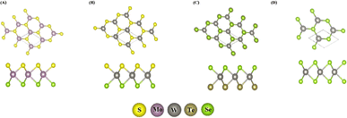 |
| | Fig. 1 Top and side views of (A) MoSSe, (B) WSSe, (C) WSeTe, and (D) WSe2 monolayers. | |
The electronic band structures of the monolayers are calculated using GGA-PBE as shown in Fig. 2. Also, the HSE06 electronic band gaps were determined and applied for the determination of both the photocatalytic and photovoltaic properties. The GGA-PBE (HSE06) electronic band gaps for the MoSSe, WSSe, and WSe2 monolayers are direct, with values of 2.028 eV, 2.195 eV and 1.967 eV respectively with the conduction band minimum (CBM) and the valence band maximum (VBM) located at the K points, while WSeTe possesses an indirect band gap of 1.775 eV as shown in Fig. 2.
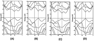 |
| | Fig. 2 Electronic GGA-PBE band structures of (A) MoSSe, (B) WSSe, (C) WSeTe, and (D) WSe2 monolayers. | |
The heterostructures of MoSSe, WSSe and WSeTe with WSe2 monolayers were constructed as shown in Fig. 3. We considered eight possible highly symmetric stacking patterns for each of the heterostructures and Fig. 3 shows MoSSe/WSe2 as an example.
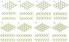 |
| | Fig. 3 Top and side view stacking patterns of MoSSe/WSe2, WSSe/WSe2, and WSeTe/WSe2 heterostructures: (A) AAI, (B) AAI-Se, (C) AAII, (D) AAII-Se, (E) ABI, (F) ABI-Se, (G) ABII, and (H) ABII-Se. | |
The AAI stacking pattern refers to the W transition metal atom of the WSe2 layer being placed on top of the metal atom of the second layer, as well as the chalcogen of WSe2 being aligned with the Janus TMD’s chalcogen atom. AAI-Se stacking is similar to AAI stacking, however WSe2 is facing Se rather than S as in AAI stacking. AAII stacking has the transition metal atom from the WSe2 monolayer on top of the chalcogen atom of the Janus TMD, while the chalcogen atom from WSe2 is on top of the metal atom of the Janus TMD. AAII-Se stacking is similar to AAII but the Se of the Janus TMD is facing towards WSe2. ABI stacking refers to the vertical alignment of metal atoms; the W from WSe2 is on top of the metal atom from the Janus TMD, but the WSe2 and Janus TMD chalcogen atoms are not vertically aligned. ABI-Se stacking is similar to ABI stacking, except that the Se atoms of the Janus TMD are facing the top WSe2 layer. ABII stacking is defined as WSe2 chalcogen atoms on top of Janus TMD metal atoms, but the WSe2 metal and Janus TMD chalcogen atoms are not vertically aligned. The ABII-Se stacking configuration is similar to ABII but the Se atoms of the Janus structure are facing towards the top WSe2 layer. The stability of the heterostructures is determined by the binding energy Eb.65,66 The formula of the binding energy is:
where
E is the total energy of the heterostructure,
E1 is the energy of the isolated MoSSe/WSeTe/WSSe monolayer and
E2 is the isolated WSe
2 monolayer’s energy. The most stable stacking mode for the MoSSe/WSe
2 heterostructure is ABI-Se, while the most stable stacking mode for the WSSe/WSe
2 and WSeTe/WSe
2 heterostructures is AAII-Se. The binding energies of the MoSSe/WSe
2, WSSe/WSe
2, and WSeTe/WSe
2 heterostructures are −0.0604 eV, −0.1721 eV, and −0.3296 eV respectively with an interlayer spacing/distance of 5.75 Å, 4.05 Å and 4.76 Å respectively.
3.2 Electronic structure
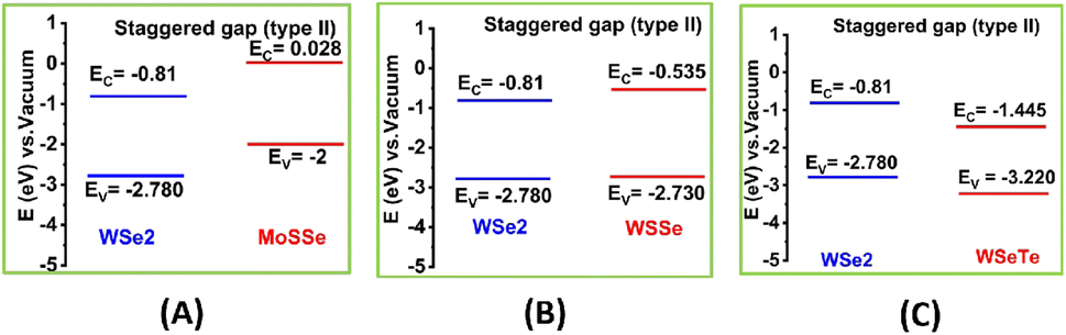
The projected electronic band structures of the most stable MoSSe/WSe2, WSSe/WSe2, and WSeTe/WSe2 vdW heterostructures calculated using GGA-PBE are shown in Fig. 4(A)–(C). The projected band structure does not provide sufficient information for identifying the band alignment, for instance in the case of WSeTe/WSe2, we cannot identify which compound the tungsten is attributed to. Therefore, we have plotted the band edge alignment for the heterostructures in Fig. 5. The band edge alignment shows that MoSSe/WSe2 and WSeTe/WSe2 are type-II band alignment semiconductors with a direct band gap of 1.093 eV and 1.603 eV respectively. The CBM and VBM of the MoSSe/WSe2 and WSeTe/WSe2 heterostructures are located at the K point in the BZ. The WSSe/WSe2 heterostructure is also a type-II band alignment semiconductor with an indirect band gap of 1.427 eV.
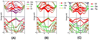 |
| | Fig. 4 Band structure of (A) MoSSe/WSe2, (B) WSSe/WSe2 and (C) WSeTe/WSe2 vdW heterostructures. Purple, green, yellow, red, and blue dots represent Mo, Se, S, W, and Te atoms, respectively. | |
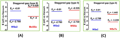 |
| | Fig. 5 Type-II band alignment of (A) MoSSe/WSe2, (B) WSSe/WSe2, and (C) WSeTe/WSe2 vdW heterostructures. | |
The transfer of photo-excited electrons and holes in type-II vdW heterostructures is advantageous for photo energy detection and harvesting. Photon absorption in a type-II heterostructure generates excited free carriers. In an ultrafast time scale, free carriers split into electrons and holes at the donor and acceptor. During the free carrier dissociation process, the electrodes will generate a photocurrent.67 The electronic band alignment of the MoSSe/WSe2, WSSe/WSe2, and WSeTe/WSe2 vdW heterostructures is shown in Fig. 5(A), (B) and (C) respectively. They all exhibit type II band alignment which facilitates efficient exciton separation and is good for the intended applications (photovoltaic solar cells and water splitting).
3.3 Photovoltaics
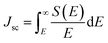
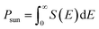
With band gaps in the optical range, the three heterostructures can also be assessed for photovoltaic applications. A standard metric to determine whether a material would be useful for photovoltaic applications is the power conversion efficiency (PCE), or the fraction of incident sunlight that can be converted into electricity. The PCE is defined as68–70| |
 | (3) |
using| |
 | (5) |
| |
 | (6) |
where VOC is the open circuit voltage, defined as the energy difference per unit charge between the band gap Eg and the inherent energy losses Eloss, S(E) is the power provided by the sun per unit area and photon energy, E is the photon energy, Jsc is the short-circuit current, or the current that can be generated by all photons with energy greater than or equal to the band gap, and FF is the fill factor. S(E) is obtained using the NREL AM1.5 dataset. The fill factor FF and the energy losses Eloss are empirical factors and cannot be calculated via first principles. A prior experimental study found that a MoS2/p-Si heterostructure exhibited a fill factor of 0.57.71 As this is the only experimental paper that the authors are aware of that reports a fill factor for a TMD, we take this to be our fill factor. The smallest Eloss that has been reported in the literature is 0.3 eV.69 We take this as our Eloss to set an upper bound on the possible power conversion efficiencies the three heterostructures could exhibit. Using eqn (3) and the HSE06 calculated band gaps for the considered heterostructures, the PCEs are calculated. The calculated PCEs for the heterostructures are 20 percent, 19.98 percent, and 18.24 percent for the MoSSe/WSe2, WSSe/WSe2, and WSeTe/WSe2 heterostructures, respectively. These values are much better than those for the InSe/Te (13.8 percent)72 vdW heterostructure, WSe2/WS2 (2.4 percent)73 vdW heterostructure, PN/WSe2 (13.8 percent)56 vdW heterostructure, type-II GaTe/InSe (9.1 percent)56 and GaTe/InS (11.52 percent)56,74 vdW heterostructure which have been recently reported.
3.4 Photocatalytic water splitting
Photocatalytic overall water splitting to form hydrogen and oxygen has received a lot of attention as a potential source of renewable energy75 that can be used to address global energy and environmental issues. The catalytic water splitting reaction (H2O → 1/2O2 + H2) is a thermodynamically uphill reaction with a net Gibbs free energy of 237 kJ mol−1.76,77 Overall water splitting for the production of H2 using a semiconductor material is similar to the photosynthetic reaction in many ways.76 In general, the photocatalytic water splitting reaction on semiconductor materials consists of three major steps, which are: (I) absorption of light irradiation with energy greater than the semiconductor band gap generates electron (e−) and hole (h+) pairs within the semiconductor material, (II) the generated electrons and holes are separated, and these charges migrate to the semiconductor interface, and (III) surface chemical reactions occur between these carriers and various compounds (e.g., H2O); electrons and holes produce H2 and O2, respectively.77,78 The preliminary requirement for application of a material in photocatalytic overall water splitting is that the redox reaction on the surface of the photocatalyst occurs when the reduction and oxidation potentials are above and below the CB and VB levels, respectively.42,58 For overall water splitting, electrons reduce water molecules to generate H2 and holes oxidize water molecules to form O2.79 The band levels of the MoSSe/WSe2, WSSe/WSe2, and WSeTe/WSe2 vdW heterostructures are shown in Fig. 6.
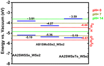 |
| | Fig. 6 Band edge alignment to HER and OER redox potentials at varying pH. The redox potentials for the hydrogen evolution reaction and the oxygen evolution reaction at pH = 0, 7, and 14 are indicated in red, olive green, and green, respectively. | |
It is important to note that under the operating conditions in an aqueous environment the relative positions of the HER and OER redox potentials to the band edges of the heterostructures will differ from the relative positions of the pH = 0 redox potentials to those of the vacuum band edges of the heterostructures. The HER and OER redox potentials are functions of pH and shift according to the Nernst equation (eqn (7))80
| | |
E(pH) = E(pH = 0) + 0.059 × pH
| (7) |
where all energies in
eqn (7) are in eV. We compare the calculated band edges to those of the HER and OER at various pH values. The relative alignment of the band edges of the heterostructures to the HER and OER potentials at pH = 0, 7, and 14 is plotted in
Fig. 6. From the figure, we can see that the WSeTe/WSe
2 heterostructure is good for full water splitting at pH 7 and 14 since the band edges straddle the redox potentials of water at these pH values. The same structure is not suitable for full water splitting at pH = 0, however even at this pH value it is good for the hydrogen evolution reaction. The MoSSe/WSe
2 heterostructure is good for the oxygen evolution reaction at pH = 7 and 14 and good for the hydrogen evolution reaction at pH = 0. The WSSe/WSe
2 heterostructure is good for the hydrogen evolution reaction at pH = 0 and pH = 7 and good for the oxygen evolution reaction at pH = 14. In general, the considered heterostructures are good for partial water splitting applications and in particular, the WSeTe/WSe
2 heterostructure is good for full water splitting under basic and acidic conditions.
3.5 Conclusion
In this study, a first principles DFT-based model was used to calculate the electronic properties of MoSSe/WSe2, WSSe/WSe2, and WSeTe/WSe2 vdW heterostructures for solar cell and photocatalytic water splitting applications. Eight different stacking modes were investigated to determine the most stable configuration based on the binding energies. In addition, the optimal interlayer spacing was determined for the considered heterostructures. From the eight stacking configurations considered, three possible vdW heterostructures were obtained as the most stable configurations, which are ABI-Se for MoSSe/WSe2, AAII-Se for WSSe/WSe2 and AAII-Se for WSeTe/WSe2. The MoSSe/WSe2 and WSeTe/WSe2 heterostructures are direct band gap materials with band gap values of 1.093 and 1.603 eV respectively, while WSSe/WSe2 has an indirect band gap of 1.427 eV. The binding energies of the MoSSe/WSe2, WSSe/WSe2, and WSeTe/WSe2 heterostructures are found to be −0.0604 eV, −0.1721 eV, and −0.3296 eV with an interlayer distance of 5.75 Å, 4.05 Å, and 4.76 Å respectively. The obtained PCE value for photovoltaic applications is 20 percent, 19.98 percent, and 18.24 percent for the MoSSe/WSe2, WSSe/WSe2, and WSeTe/WSe2 heterostructures, respectively, which is good and makes the structures promising for this application. In addition, the band edge alignment is type two which assists charge separation, and coupled with the intrinsic polar nature of Janus materials, this strengthens their application for photovoltaics. Regarding the photocatalytic water splitting application we found out that the WSeTe/WSe2 heterostructure is good for full water splitting under basic and acidic conditions. We also found out that not all of these heterostructures can satisfy the band edge requirements for full water splitting, however they can be applied in the H2 evolution reaction and oxygen evolution reaction under visible light irradiation. In general, this study reveals that making Janus heterostructures is a good way to tune the electronic properties and engineer materials for photovoltaics and photocatalytic water splitting.
Conflicts of interest
There are no conflicts to declare.
Acknowledgements
This work was substantially sponsored by funding from Addis Ababa University through a thematic project (Grant No. RD/LT-095/2019). We also gratefully acknowledge Dr Tekalign T. Debela, Postdoctoral Associate at the University of Oregon, for providing insight and expertise that considerably aided the research. The authors thank the Centre for High Performance Computing (CHPC) in Cape Town, South Africa, for the computational resources used in this study. Samuel acknowledges the Space Science and Geospatial Institute for financial support, and KOO acknowledges the HySA Infrastructure Centre of Competence, Faculty of Engineering, North-West University for their financial support.
References
- A. Kuc, T. Heine and A. Kis, MRS Bull., 2015, 40, 577–584 CrossRef CAS.
- B. T. Beshir, K. O. Obodo and G. A. Asres, RSC Adv., 2022, 12, 13749–13755 RSC.
- A. Rawat, R. Ahammed, Dimple, N. Jena, M. K. Mohanta and A. De Sarkar, J. Phys. Chem. C, 2019, 123, 12666–12675 CrossRef CAS.
- G. A. Asres, A. Dombovari, T. Sipola, R. Puskás, A. Kukovecz, Z. Kónya, A. Popov, J.-F. Lin, G. S. Lorite and M. Mohl, et al., Sci. Rep., 2016, 6, 1–7 Search PubMed.
- Z. Zhu, K. Ren, H. Shu, Z. Cui, Z. Huang, J. Yu and Y. Xu, Catalysts, 2021, 11, 991 CrossRef CAS.
- S. Z. Butler, S. M. Hollen, L. Cao, Y. Cui, J. A. Gupta, H. R. Gutiérrez, T. F. Heinz, S. S. Hong, J. Huang and A. F. Ismach, et al., ACS Nano, 2013, 7, 2898–2926 CrossRef CAS PubMed.
- K. Obodo, G. Gebreyesus, C. Ouma, J. Obodo, S. Ezeonu, D. Rai and B. Bouhafs, RSC Adv., 2020, 10, 15670–15676 RSC.
- M. Mohl, A.-R. Rautio, G. A. Asres, M. Wasala, P. D. Patil, S. Talapatra and K. Kordas, Adv. Mater. Interfaces, 2020, 7, 2000002 CrossRef CAS.
- K. Obodo, C. Ouma, J. Obodo, G. Gebreyesus, D. Rai, A. Ukpong and B. Bouhafs, Nanotechnology, 2021, 32, 355502 CrossRef CAS PubMed.
- I. C. Onyia, S. O. Ezeonu, D. Bessarabov and K. O. Obodo, Comput. Mater. Sci., 2021, 197, 110613 CrossRef CAS.
- K. O. Obodo, N. Chetty and J. Obodo, Comput. Mater. Sci., 2017, 128, 373–378 CrossRef CAS.
- A. K. Sibhatu, G. A. Asres, A. Yimam and T. Teshome, RSC Adv., 2022, 12, 21270–21279 RSC.
- K. O. Obodo, C. N. M. Ouma, J. T. Obodo and M. Braun, Phys. Chem. Chem. Phys., 2017, 19, 19050–19057 RSC.
- K. O. Obodo, C. N. Ouma, G. Gebreyesus, J. T. Obodo, S. O. Ezeonu and B. Bouhafs, Mater. Res. Express, 2019, 6, 106307 CrossRef CAS.
- E. Singh, K. S. Kim, G. Y. Yeom and H. S. Nalwa, RSC Adv., 2017, 7, 28234–28290 RSC.
- F. Li, W. Wei, P. Zhao, B. Huang and Y. Dai, J. Phys. Chem. Lett., 2017, 8, 5959–5965 CrossRef CAS PubMed.
- K. O. Obodo, C. N. M. Ouma, J. T. Obodo, M. Braun and D. Bessarabov, Comput. Condens. Matter, 2019, 21, e00419 CrossRef.
- Y. Yang, Y. Zhang, H. Ye, Z. Yu, Y. Liu, B. Su and W. Xu, Superlattices Microstruct., 2019, 131, 8–14 CrossRef CAS.
- D. Muoi, N. N. Hieu, H. T. Phung, H. V. Phuc, B. Amin, B. D. Hoi, N. V. Hieu, L. C. Nhan, C. V. Nguyen and P. Le, Chem. Phys., 2019, 519, 69–73 CrossRef CAS.
- K. O. Obodo, C. N. Ouma, G. Gebreyesus, J. T. Obodo and M. Braun, 2018 Open Innovations Conference, OI, 2018, pp. 115–119 Search PubMed.
- Q. Cheng, J. Pang, D. Sun, J. Wang, S. Zhang, F. Liu, Y. Chen, R. Yang, N. Liang and X. Lu, et al., InfoMat, 2020, 2, 656–697 CrossRef CAS.
- H. Li, G. Lu, Y. Wang, Z. Yin, C. Cong, Q. He, L. Wang, F. Ding, T. Yu and H. Zhang, Small, 2013, 9, 1974–1981 CrossRef CAS PubMed.
- H. Zeng, G.-B. Liu, J. Dai, Y. Yan, B. Zhu, R. He, L. Xie, S. Xu, X. Chen and W. Yao, et al., Sci. Rep., 2013, 3, 1–5 Search PubMed.
- R. Tenne and A. Wold, Appl. Phys. Lett., 1985, 47, 707–709 CrossRef CAS.
- G. Kakavelakis, A. E. Del Rio Castillo, V. Pellegrini, A. Ansaldo, P. Tzourmpakis, R. Brescia, M. Prato, E. Stratakis, E. Kymakis and F. Bonaccorso, ACS Nano, 2017, 11, 3517–3531 CrossRef CAS PubMed.
- H. Li, J. Wu, Z. Yin and H. Zhang, Acc. Chem. Res., 2014, 47, 1067–1075 CrossRef CAS PubMed.
- S. Ahn, G. Kim, P. K. Nayak, S. I. Yoon, H. Lim, H.-J. Shin and H. S. Shin, ACS Nano, 2016, 10, 8973–8979 CrossRef CAS PubMed.
- I. C. Gerber and X. Marie, Phys. Rev. B, 2018, 98, 245126 CrossRef CAS.
- N. Liu, X. D. Weiss and H.-C. Cheng, Nat. Rev. Mater., 2016, 1(9), 1–17 Search PubMed.
- S. Yu, W. Wei, F. Li, B. Huang and Y. Dai, Phys. Chem. Chem. Phys., 2020, 22, 25675–25684 RSC.
- M. Yagmurcukardes, Y. Qin, S. Ozen, M. Sayyad, F. M. Peeters, S. Tongay and H. Sahin, Appl. Phys. Lett., 2020, 7, 011311 CAS.
- L. Cao, Y. S. Ang, Q. Wu and L. Ang, Appl. Phys. Lett., 2019, 115, 241601 CrossRef.
- S. Li, M. Shi, J. Yu, S. Li, S. Lei, L. Lin and J. Wang, Chin. Chem. Lett., 2021, 32, 1977–1982 CrossRef CAS.
- J. Wang, H. Shu, T. Zhao, P. Liang, N. Wang, D. Cao and X. Chen, Phys. Chem. Chem. Phys., 2018, 20, 18571–18578 RSC.
- L. Dong, J. Lou and V. B. Shenoy, ACS Nano, 2017, 11, 8242–8248 CrossRef CAS PubMed.
- R. K. Defo, S. Fang, S. N. Shirodkar, G. A. Tritsaris, A. Dimoulas and E. Kaxiras, Phys. Rev. B, 2016, 94, 155310 CrossRef.
- T. Hu, F. Jia, G. Zhao, J. Wu, A. Stroppa and W. Ren, Phys. Rev. B, 2018, 97, 235404 CrossRef CAS.
- H. Xiong, J. Sobota, S.-L. Yang, H. Soifer, A. Gauthier, M.-H. Lu, Y.-Y. Lv, S.-H. Yao, D. Lu and M. Hashimoto, et al., Phys. Rev. B, 2017, 95, 195119 CrossRef.
- K. Zhang, J. K. Kim, B. Park, S. Qian, B. Jin, X. Sheng, H. Zeng, H. Shin, S. H. Oh and C.-L. Lee, et al., Nano Lett., 2017, 17, 6676–6683 CrossRef CAS PubMed.
- X. Li, Y. Dai, M. Li, W. Wei and B. Huang, J. Mater. Chem. A, 2015, 3, 24055–24063 RSC.
- X. Ma, X. Wu, H. Wang and Y. Wang, J. Mater. Chem. A, 2018, 6, 2295–2301 RSC.
- M. Idrees, H. Din, R. Ali, G. Rehman, T. Hussain, C. Nguyen, I. Ahmad and B. Amin, Phys. Chem. Chem. Phys., 2019, 21, 18612–18621 RSC.
- Y. Cai, G. Zhang and Y.-W. Zhang, J. Am. Chem. Soc., 2014, 136, 6269–6275 CrossRef CAS PubMed.
- Y. Zhao, J. Qiao, Z. Yu, P. Yu, K. Xu, S. P. Lau, W. Zhou, Z. Liu, X. Wang and W. Ji, et al., Adv. Mater., 2017, 29, 1604230 CrossRef PubMed.
- A.-Y. Lu, H. Zhu, J. Xiao, C.-P. Chuu, Y. Han, M.-H. Chiu, C.-C. Cheng, C.-W. Yang, K.-H. Wei and Y. Yang, et al., Nat. Nanotechnol., 2017, 12, 744–749 CrossRef CAS PubMed.
- J. Li, Z. Huang, W. Ke, J. Yu, K. Ren and Z. Dong, J. Alloys Compd., 2021, 866, 158774 CrossRef CAS.
- K. Ren, Y. Luo, S. Wang, J.-P. Chou, J. Yu, W. Tang and M. Sun, ACS Omega, 2019, 4, 21689–21697 CrossRef CAS PubMed.
- K. Ren, J. Yu and W. Tang, J. Alloys Compd., 2020, 812, 152049 CrossRef CAS.
- K. Ren, J. Yu and W. Tang, J. Appl. Phys., 2019, 126, 065701 CrossRef.
- C.-H. Lee, G.-H. Lee, A. M. Van Der Zande, W. Chen, Y. Li, M. Han, X. Cui, G. Arefe, C. Nuckolls and T. F. Heinz, et al., Nat. Nanotechnol., 2014, 9, 676–681 CrossRef CAS PubMed.
- R. Meng, J. Jiang, Q. Liang, Q. Yang, C. Tan, X. Sun and X. Chen, Sci. China Mater., 2016, 59, 1027–1036 CrossRef CAS.
- T. Roy, M. Tosun, J. S. Kang, A. B. Sachid, S. B. Desai, M. Hettick, C. C. Hu and A. Javey, ACS Nano, 2014, 8, 6259–6264 CrossRef CAS PubMed.
- M.-Y. Li, C.-H. Chen, Y. Shi and L.-J. Li, Mater. Today, 2016, 19, 322–335 CrossRef CAS.
- P. Giannozzi, S. Baroni, N. Bonini, M. Calandra, R. Car, C. Cavazzoni, D. Ceresoli, G. L. Chiarotti, M. Cococcioni and I. Dabo, et al., J. Phys.: Condens. Matter, 2009, 21, 395502 CrossRef PubMed.
- J. P. Perdew, K. Burke and M. Ernzerhof, Phys. Rev. Lett., 1996, 77, 3865 CrossRef CAS PubMed.
- X. Zheng, Y. Wei, K. Pang, N. Kaner Tolbert, D. Kong, X. Xu, J. Yang, X. Li and W. Li, Sci. Rep., 2020, 10, 1–9 CrossRef PubMed.
- J. Heyd, G. E. Scuseria and M. Ernzerhof, J. Chem. Phys., 2003, 118, 8207–8215 CrossRef CAS.
- Y. Luo, K. Ren, S. Wang, J.-P. Chou, J. Yu, Z. Sun and M. Sun, J. Phys. Chem. C, 2019, 123, 22742–22751 CrossRef CAS.
- B. Ghosh, S. Nahas, S. Bhowmick and A. Agarwal, Phys. Rev. B, 2015, 91, 115433 CrossRef.
- B.-J. Wang, X.-H. Li, R. Zhao, X.-L. Cai, W.-Y. Yu, W.-B. Li, Z.-S. Liu, L.-W. Zhang and S.-H. Ke, J. Mater. Chem. A, 2018, 6, 8923–8929 RSC.
- M. Idrees, H. Din, S. U. Rehman, M. Shafiq, Y. Saeed, H. Bui, C. V. Nguyen and B. Amin, Phys. Chem. Chem. Phys., 2020, 22, 10351–10359 RSC.
- J. Lou, K. Ren, Z. Huang, W. Huo, Z. Zhu and J. Yu, RSC Adv., 2021, 11, 29576–29584 RSC.
- A. Rawat, M. K. Mohanta, N. Jena, Dimple, R. Ahammed and A. De Sarkar, J. Phys. Chem. C, 2020, 124, 10385–10397 CrossRef CAS.
- L. Cao, Y. Deng, H. Gao, Y. Wang, X. Chen and Z. Zhu, Phys. Chem. Chem. Phys., 2015, 17, 6809–6818 RSC.
- K. O. Obodo, C. N. M. Ouma, P. M. Modisha and D. Bessarabov, Appl. Surf. Sci., 2020, 529, 147186 CrossRef CAS.
- S. Wang, C. Ren, H. Tian, J. Yu and M. Sun, Phys. Chem. Chem. Phys., 2018, 20, 13394–13399 RSC.
- Y. Zhang, R. Xiong, B. Sa, J. Zhou and Z. Sun, Sustainable Energy Fuels, 2021, 5, 135–143 RSC.
- M. R. Filip, C. Verdi and F. Giustino, J. Phys. Chem. C, 2015, 119, 25209–25219 CrossRef CAS.
- H. J. Snaith, Adv. Funct. Mater., 2010, 20, 13–19 CrossRef CAS.
- W. Shockley and H. J. Queisser, J. Appl. Phys., 1961, 32, 510–519 CrossRef CAS.
- S. K. Pradhan, B. Xiao and A. K. Pradhan, Sol. Energy Mater. Sol. Cells, 2016, 144, 117–127 CrossRef CAS.
- Z. Ma, R. Li, R. Xiong, Y. Zhang, C. Xu, C. Wen and B. Sa, Materials, 2021, 14, 3768 CrossRef CAS PubMed.
- P. Lin and J. Yang, J. Alloys Compd., 2020, 842, 155890 CrossRef CAS.
- J. Chen, X. He, B. Sa, J. Zhou, C. Xu, C. Wen and Z. Sun, Nanoscale, 2019, 11, 6431–6444 RSC.
- K. Maeda and K. Domen, J. Phys. Chem. Lett., 2010, 1, 2655–2661 CrossRef CAS.
- K. Maeda, J. Photochem. Photobiol., C, 2011, 12, 237–268 CrossRef CAS.
- L. Shi, B. Yan, D. Shao, F. Jiang, D. Wang and A. Lu, Catal, 2017, 38, 389–395 CAS.
- B. Y. Alfaifi, H. Ullah, S. Alfaifi, A. A. Tahir and T. K. Mallick, Veruscript Funct. Nanomater., 2018, 2, BDJOC3 CrossRef.
- J. Wang, X. Yang, J. Cao, Y. Wang and Q. Li, Comput. Mater. Sci., 2018, 150, 432–438 CrossRef CAS.
- T. Shinagawa and K. Takanabe, ChemSusChem, 2017, 10, 1318–1336 CrossRef CAS PubMed.
|
| This journal is © The Royal Society of Chemistry 2022 |
Click here to see how this site uses Cookies. View our privacy policy here. 
 Open Access Article
 This Open Access Article is licensed under a Creative Commons Attribution-Non Commercial 3.0 Unported Licence
 *a
*a