
 Open Access Article
 This Open Access Article is licensed under a Creative Commons Attribution-Non Commercial 3.0 Unported Licence
Mechanism and principle of doping: realizing of silver incorporation in CdS thin film via doping concentration effect
A. S Najm *ag,
Abdulwahab Aljuhanib,
Hasanain Salah Naeemc,
K. Sopiand,
Raid A. Ismaile,
Araa Mebdir Holif,
Laith S. Sabrig,
Asla Abdullah AL-Zahranih,
Rashed Taleb Rasheede and
Hazim Moriai
*ag,
Abdulwahab Aljuhanib,
Hasanain Salah Naeemc,
K. Sopiand,
Raid A. Ismaile,
Araa Mebdir Holif,
Laith S. Sabrig,
Asla Abdullah AL-Zahranih,
Rashed Taleb Rasheede and
Hazim Moriai
aDepartment of Electrical, Electronics and System, FKAB, Universiti Kebangsaan Malaysia (UKM), 43600 Bangi, Selangor, Malaysia. E-mail: asmaa.soheil@yahoo.com
bDepartment of Chemical Engineering Technology, Yanbu Industrial College, Yanbu Al-Sinaiyah City 41912, Kingdom of Saudi Arabia
cAl-Muthanna University, 66001 Samawah, Al Muthanna, Iraq
dDepartment of Chemical Engineering and Petroleum Industries, Al-Mustaqbal University College, Babylon 51001, Iraq
eSolar Energy Research Institute (SERI), Universiti Kebangsaan Malaysia (UKM), 43600 Bangi, Selangor, Malaysia
fApplied Sciences Department, University of Technology, Baghdad, Iraq
gDepartment of Physics, College of Education, University of Al-Qadisiyah, Al-Diwaniyah, Al-Qadisiyah 58002, Iraq
hDepartment of Chemical Engineering, University of Technology, Baghdad, Iraq
iImam Abdulrahman-bin Fiasal University, Eastern Region, Dammam, Saudi Arabia
First published on 17th October 2022
Abstract
A high-quality buffer layer serves as one of the most significant issues that influences the efficiency of solar cells. Doping in semiconductors is an important strategy that can be used to control the reaction growth. In this study, the influence of Ag doping on the morphological, optical and electrical properties of CdS thin films have been obtained. Herein, we propose the mechanism of CdS film formation with and without Ag ions, and we found that changes in the reaction of preparing CdS by the chemical bath deposition (CBD) method cause a shift in the geometric composition of the CdS film. XRD showed that the position of peaks in the doped films are displaced to wider angles, indicating a drop in the crystal lattice constant. The optical analysis confirmed direct transition with an optical energy gap between 2.10 and 2.43 eV. The morphological studies show conglomerates with inhomogeneously distributed spherical grains with an increase of the Ag ratio. The electrical data revealed that the annealed Ag-doped CdS with 5% Ag has the highest carrier concentration (3.28 × 1015 cm−3) and the lowest resistivity (45.2 Ω cm). According to the results, the optimal Ag ratio was obtained at Ag 5%, which encourages the usage of CdS in this ratio as an efficient buffer layer on photovoltaic devices.
Introduction
Environmental regulation and the rapid depletion of fossil resources have forced us to explore eco-friendly energy sources.1 Recently, II–VI group based semiconductor nanomaterials have expected a lot of attention owing to their prospective applications in electronic and optoelectronic fields. Cadmium sulphide (CdS) is an essential II–VI compound semiconductor, with high transparency, direct bandgap transition (Eg ∼ 2.4 eV), high electron affinity (4.2 eV) and n-type conductivity.2 CdS is the most commonly implemented n-type buffer layer for thin-film solar cells with excellent performance.3 As a buffer layer, for optimum minority carrier transport, CdS ought to be as thin as possible to ensure low series resistance, as a thicker film might reduce the Schottky barrier's effectiveness. Consequently to enhance the CdS conductivity, a specific process called doping is achieved by introducing impurities into the semiconductor crystal intentionally, which can be either acceptor or donor atoms in their crystalline lattice.4Doping was achieved chemically throughout the process of growth, it is possible to carry out the procedure on-site by simply adding controlled quantities of a solution of a salt of the doping atom to the reaction solution, without any sensitive damage to the lattice.5 Even though, there are some research reports on many elements doped CdS, most of the studies are focused on nano-powders and the reports on thin films are very limited and require more understanding. Chandramohan et al. (2009) clarified that the considerable influence of Co, alters the optical band gap of CdS by generating localized energy states at the band boundaries.6 While, Sebastian (1993) showed that utilizing Cu as a doping element during the CBD process resulted in a drop in CdS bandgap energy of as little as 2.0 eV.7 Identical outcomes for the bandgap energy were reported by Portillo-Moreno et al. (2006), it has been obtained that the resistivity of CdS increases with doping of Cu.8 Sánchez et al. (2014) described how the voltage of the solar cell is increased by using doped-Cu CdS as the window layer in CZTS; this could aid in resolving the deficit voltage issue in this type of device.9 In addition, it has been shown by Challa et al. (2012) that adequate boron doping may substantially lower the dark resistivity and improve the photosensitivity of CdS thin films.10
Hani Khallaf investigated the effect of four elements namely (Al, Ga, B, and In) by in situ doping of CdS using CBD, and proved it to be successful.11–13 The bandgap of CdS-doped films was observed to drop considerably when the [Al, Ga, B, and In]/[Cd] ratio in the solution increased in all cases. Alhammadi et al. (2018) study the impact of Ga doping of the CdS buffer layer on the performance of CIGS solar-cell. The photo electrochemical results revealed that, the density of photocurrent was enhanced, and the efficiency of CIGS cell fabricated using CdS![[thin space (1/6-em)]](https://www.rsc.org/images/entities/char_2009.gif) :Ga was slightly improved from 9.69% to 10.37%.14
:Ga was slightly improved from 9.69% to 10.37%.14
Ag, a group I element, improves the electrical characteristics of (II–VI) semiconductors by acting as a donor dopant. The transport of the electron between the doped metal and the semiconductor matrix is facilitated by the differences in potential between the cadmium sulphide conduction band and the silver Fermi level.15 Taur and co-workers examined the influence of annealing on optoelectronic and physicochemical properties and revealed that the response of the I–V achieved from as grown and annealed thin films exhibit an increase in photosensitivity from 72 to 96% upon illumination to 100 mW cm−2 light source.16 While Ferrá-gonzález et al. (2014) noticed that the roughness and bandgap energy increase slightly with the silver concentration, and silver sulphide (Ag2S) starts forming when the cadmium is consumed and no longer replaced, the bandgap and roughness of the films now start to diminish as the AgNO3 concentration increases.17 Pacheco et al. (2017) found that the presence of a polycrystalline structure for the Ag+ doped had an impact on quantum confinement, with the average particle size decreasing from (5.46 to 4.12) nm, leading to higher-energy emissions as the particle size decreased below the effective CdS exciton Bohr radius.18
Lots of techniques are available in the recent times and used by researcher's in the doping deposition of CdS thin films of different materials on various substrates. Although, many researchers study the effect of Ag doping using different deposition methods, by CBD method is still limited reports has been achieved. In our case, the CBD growth process was utilized to deposit and to dope CdS thin films at the same time. Through the relatively simple process, CBD yields well adherent and homogeneous thin films with good reproducibility. We have observed from that compare with other methods, in situ doping by CBD has been extensively utilized to reduce the dark resistivity of CdS thin films grown and maintain the CdS film quality and transparency for electronic and optoelectronic applications.19
Hence, in this work, improvement of the CdS thin film doping concept by a fundamental understanding of the impact of doping on optical, morphological, structural, and electrical characterization was studied in detail and discussed. Also, we provide the mechanism that affects the formation of CdS thin film. The crystalline size and CdS thin film surface morphology were identified to have great understanding of the effect different doping concentration ratios.
Methodology
Methods and experiments
CdS thin film was prepared according to our previous work.20 Ultrasonically cleaned and degreased soda-lime glass substrates of size 5 cm × 5 cm. The key precursors for CdS are aqueous solutions from Cadmium Sulfate, (CdSO4, Aldrich, purity 98%) and Thiourea, (SC(NH2)2 Merck, ≥98%), and Silver Nitrate (AgNO3, Alfa Aesar, purity 99.99%).For silver doping stock, Silver Nitrate (AgNO3) was dissolved in deionized water (DI) to obtain 0.01 M solution.
Firstly, we placed ∼350 ml of DIW in the clean growth beaker. Then, it was added 20 ml of NH4OH solution to the growth beaker. A magnetic stirrer is placed inside the growth beaker and the stirring speed was set to 360 rpm, and heated until reached 80 °C. The substrates were introduced to the bath once its temperature is stabilized. Secondly, in a separate beaker that contains CdSO4 powder, 20 ml NH4OH solution was added and placed in the ultrasonic bath for 10 minutes. Thirdly, in another separate beaker, 10 ml DI water was added to the thiourea powder and also put in the ultrasonic bath for 10 minutes.
Then Cd salt beaker was added to the growth beaker. After 3 minutes, the thiourea solution was then added to the chemical bath. The final solution volume was 400 ml (350 ml DIW + 20 ml NH4OH mixed with CdSO4 + 10 ml DIW mixed with thiourea + 20 ml NH4OH added to growth beaker). The pH is set to 9. Then after, the reaction time was set to 30 minutes.
This is for preparation of CdS undoped Ag. In the following step, AgNO3 solution has been mixed with the CdSO4 salt before adding to growth beaker and placed in the ultrasonic bath for 10 minutes. (The concentration was varied by 1, 5, and 10% of 0.002 M cadmium sulfate concentration to adjust the molar ratio of silver within CdS lattice). Then after, the remaining steps are repeated as the same as in the method of preparing of CdS undoped. An annealing process in air was performed after the deposited CdS layer was completely dry. This air annealing process was carried out for 10 minutes at different temperatures from (150–450) °C. Fig. 1, shows the schematic diagram of the synthesis process for CdS thin film.
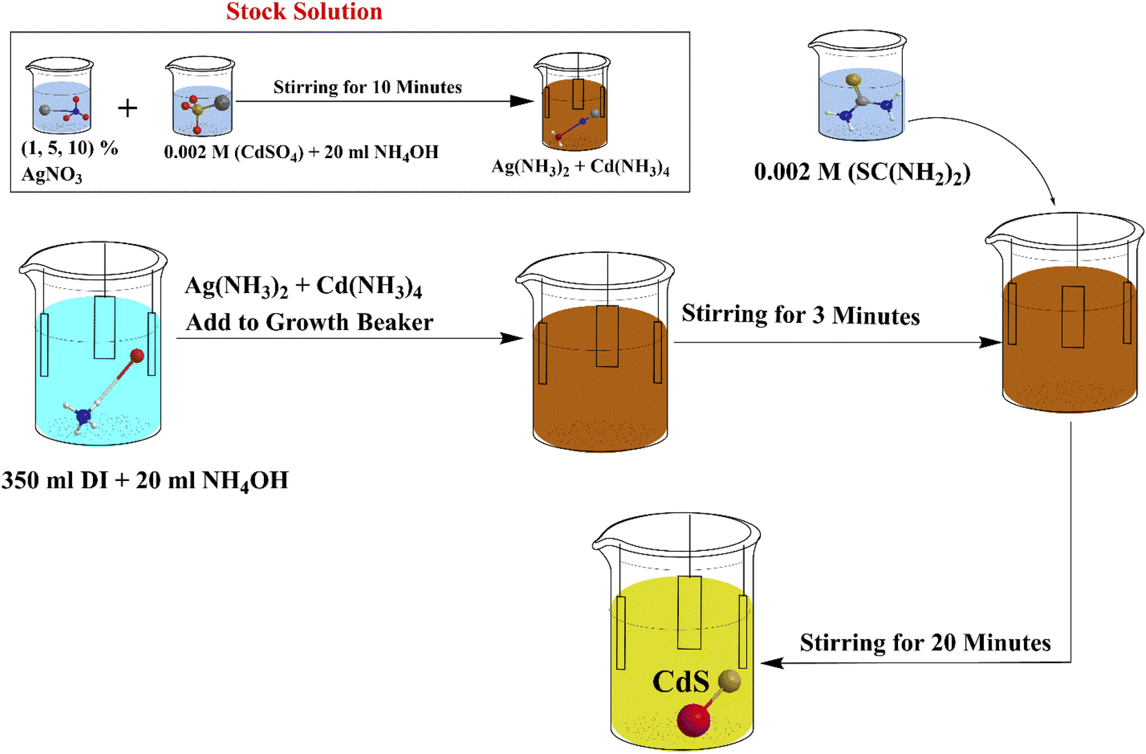 | ||
| Fig. 1 CBD doping of CdS thin film synthesis: experimental steps. | ||
Characterization
A Lambda 950 UV/vis/NIR spectrometer was used to test optical characteristics in the range of 300 nm to 600 nm (PerkinElmer, USA). At room temperature, an AXS-D8 Advance Cu-K diffractometer was used to investigate the films' structural characteristics (Bruker Corp., USA). XRD patterns examined in a 2θ range, with a step size of 0.02°, which ranged between 10° and 80°, using the Cu-Kα radiation wavelength, λ, of 1.5408 Å. FEI Quanta 400F field emission scanning electron microscope (FESEM) equipped with Oxford-Instruments INCA 400 X-Max detector for energy-dispersive X-ray spectroscopy (EDX) measurement at ×300 magnification (spot size 1 mm × 1 mm) and an accelerating voltage of 20 kV. Finally, the electrical properties of films were measured using the HMS ECOPIA 3000 Hall Effect measuring device with a 0.57 T magnetic field and 45 nA probe current, Fig. 2, showed the Hall effect device.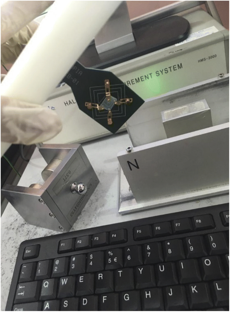 | ||
| Fig. 2 Hall effect device. | ||
Results and discussion
Analysis of optical properties
UV–vis absorption spectrum of CdS film before and after doping with Ag in the range (300–600) nm is shown in Fig. 3. This figure showed that the undoped CdS film has higher absorbance than those of the doped films. The reduction in absorbance may be ascribed to the defect states resulting from the imperfections in the lattice structure caused by the varying Ag concentrations.17 Essentially, there are fewer defects and impurities in a sharper edge in the undoped CdS sample, because the higher rates of impinging particles led to increased film growth. It could be seen that the uniformity of the film causes these variations.21 By applying Tauc's figure and the essential absorption edge that corresponds to the semiconductor direct energy gap, the values of the optical energy gap are obtained,22 as shown in Fig. 4. The optical energy gap (Eopt) and optical absorption coefficient (α) are related in the direct transition semiconductor, as:
 | (1) |
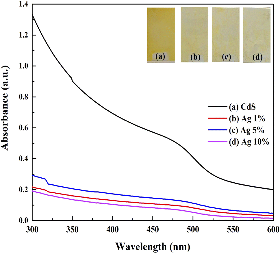 | ||
| Fig. 3 Optical absorbance spectra of undoped CdS film and CdS film doped with Ag. | ||
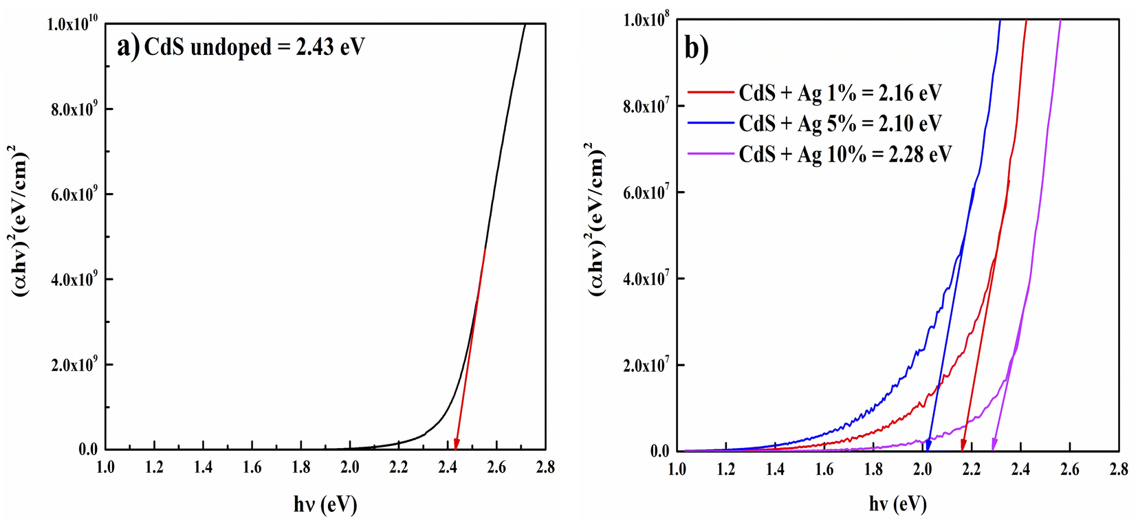 | ||
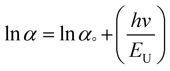
| Fig. 4 Tauc plot of (αhν)2 versus hν for: (a) CdS undoped, (b) CdS doped films. | ||
Regarding the extrapolation of the linear region of the curves to the horizontal axis intercept, the recorded values of energy gap were 2.43, 2.16, 2.10, and 2.28 eV for undoped CdS, CdS: 1% Ag, CdS: 5% Ag, and CdS: 10% Ag, respectively. As shown, the doping decreases the energy gap of the CdS film because of forming of trap states and impurities in the region of the energy gap of the film. During the preparation of thin films, a variety of defects may be created, such as voids, interstitials, dislocations, strains, etc. These defects play a vital role in the variation of the optical absorption as centers of the trap. Hence, due to the formation of localized energy states along the band edges, a reduction in the energy gap may mostly be attributed to the defect band tailing. The results confirm that Ag substitutes Cd sites more as compared to interstitially at lower doping and Ag enters interstitially more as compared to substitutional at higher Ag doping. In the substitutional position.
Essentially, it acts as an accepter and at the interstitial position, it acts as a donor. Consequently, it produces donor and accepter levels below and above the conduction and valence band, respectively. Thus, the decrease in energy gap of the film after Ag doping is attributed to the creation of additional energy levels in the CdS film's energy gap, which results in the broadening of the band of the film and hence decreases its energy gap. A similar decrease in the bandgap after doping of Ag in CdS thin films prepared by closed space sublimation (CSS) techniques has been observed by Rehman et al. (2003).23 It takes longer for photon energies to drop below the bandgap energy for absorption to decrease than it does for higher energies.24
Similar to the absorption in a severely doped crystalline semiconductor, sub-band absorption is determined by the Urbach law, which is based on the typical distribution or width of band tail states.25 Urbach tail is achieved at low crystalline, disorderly and amorphous substances because they are located in states which extend the bandgap.26,27 The spectral dependency of absorption coefficient (α) and photon energy (hv) is known as the empirical rule for Urbach in the low photon energy range as follows:
|
α = α°exp(hv/EU)
| (2) |
 | (3) |
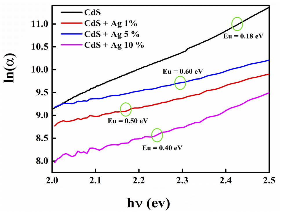 | ||
| Fig. 5 Urbach energy of undoped and doped CdS films with different percentage ratios of Ag. | ||
The lowest Urbach energy was found to be 0.18 eV for undoped CdS, which indicates that the high crystallinity and low defects deposited CdS film. While, the Urbach energy increases with increasing the doping concentration such as 0.50, 0.60, and 0.40 eV for Ag-doped CdS films with 1, 5, and 10% respectively, the increased disorder in the film might be related to surface roughness arising as shown in Table 1.29
| Samples | Eg (eV) | Eu (eV) |
|---|---|---|
| CdS | 2.43 | 0.18 |
| CdS + 1% Ag | 2.16 | 0.50 |
| CdS + 5% Ag | 2.10 | 0.60 |
| CdS + 10% Ag | 2.28 | 0.40 |
Structural properties
The impact of doping on the crystallization behavior of the examined thin films is explored by using X-ray diffraction.30 The films were scanned from 10° to 80°. The XRD patterns of undoped and Ag-doped CdS thin films are revealed in Fig. 6. The CdS film mainly forms cubic and hexagonal phases based on the conditions of the deposition. Besides, it is difficult to detect the precise crystal structure of a CdS thin film, whether the film is mostly hexagonal, predominantly cubic, or a combination of both, because both film phases have the same XRD diffraction peak angles.31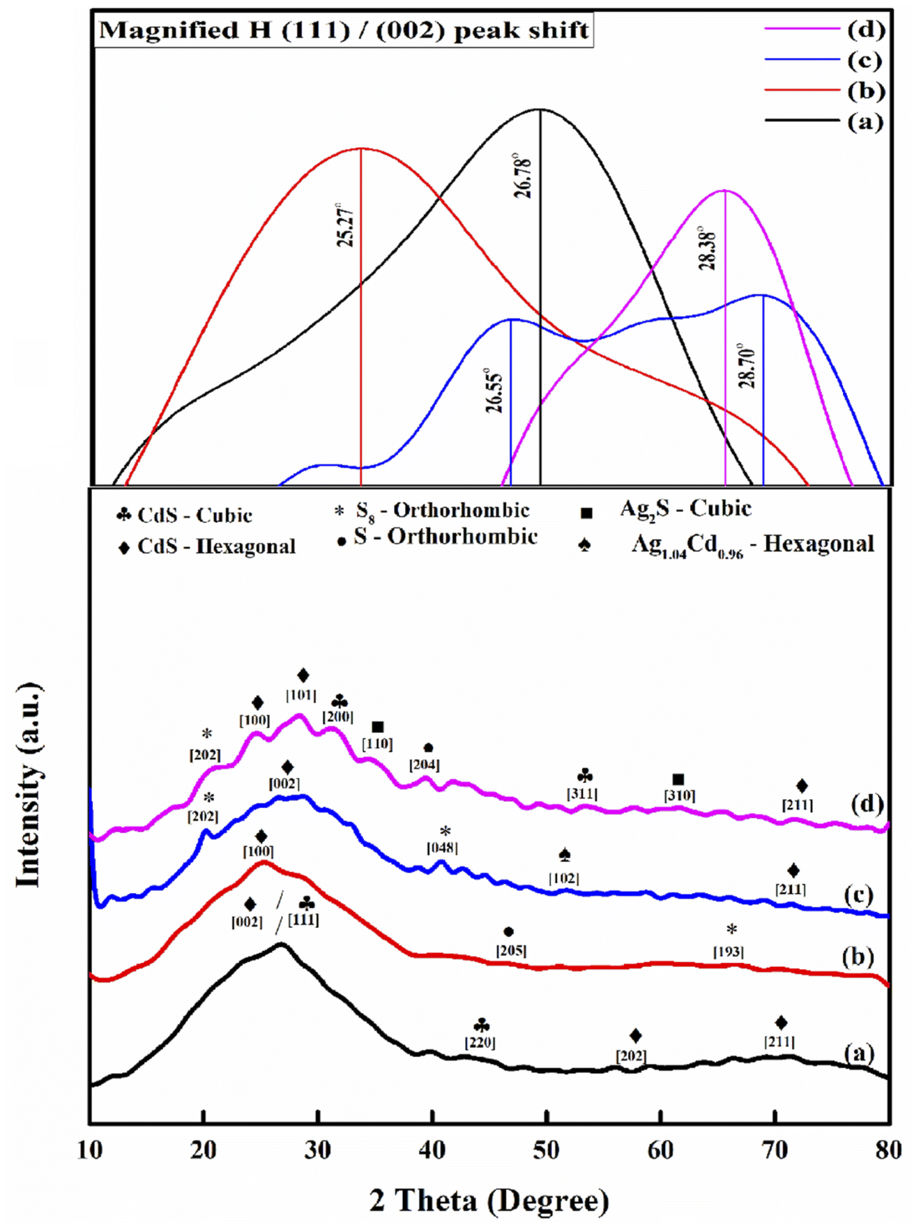 | ||
| Fig. 6 XRD patterns of (a) undoped CdS, Ag-doped CdS at (b) 1%, (c) 5%, (d) 10%. | ||
Simply, each sample shows different behaviors relevant to the concentration of Ag add in this situation. For the basic CdS pattern Fig. 6(a), the main strong peak was found at 2θ = 26.78° indexed to both (002) and (111) planes, which corresponds to the hexagonal phase of CdS follow to JCPDS-01-080-0006 and the cubic phase of CdS and according to JCPDS-89-0440, respectively. Many strong diffraction peaks oriented along the (100), (002) and (101) planes show that the deposited films are polycrystalline, which has been appearing at Ag ratio of 1%, 5% and 10%, respectively. These diffraction planes belong to the CdS crystal hexagonal phase (JCPDS card no. 06-0314). Indeed, as the ratio of Ag dopant increased, the hexagonal phase is more stable and the favored orientation.
The relative intensity of all CdS characteristic peaks has been significantly changed from their previous positions to that of before doping. This is attributed to the interest doping, which is favorable when the ion radii between two elements are comparable. The ionic radius of Ag2+ is around 0.94 Å, which is more comparable with Cd2+ with ionic radius of 0.95 Å, however, there is a significant difference with S2− (1.84 Å). Therefore, there is a possibility in lattice sites of an electron transfer from Ag2+ to Cd2+ resulting in a decrease of the lattice constant and the crystalline plane distance. Since there is no peak of pure metal silver, the possibility of silver doping is because of the interstitial sites of principle components in CdS layer structure. As a result, Ag-doping will induce a small change towards lower diffraction angles relative to pure CdS thin film.
In Ag-doped CdS films, the smaller shifts in the peak position led to more the incorporation of Ag2+ into the CdS lattice, contributing to the formulation of Ag1.04Cd0.96, only in the case of doping with Ag 5%, and Ag2S for Ag 10%. The diffraction peaks for Ag1.04Cd0.96 at Ag 5% which is corresponding to 51.8°, matching the hexagonal phase (JCPDS-03-065-5678). While Ag2S at 2θ = 34.6 and 61.3° indexed to both (110) and (310) planes, matching the cubic phase of (JCPDS-00-001-1151).
Morphological analysis
The morphology of chalcogenide films can have a significant influence on their properties. This is especially relevant for solar cells, as grain boundary and surface roughness have a direct effect on film recombination. As a result, surface morphology and the presence of impurities will influence photovoltaic device operating conditions.36 The micrograph reveals that the deposited film without doping has spheroid-like grains, and the glass substrate is well covered without pinholes or cracks, as shown in Fig. 7(a).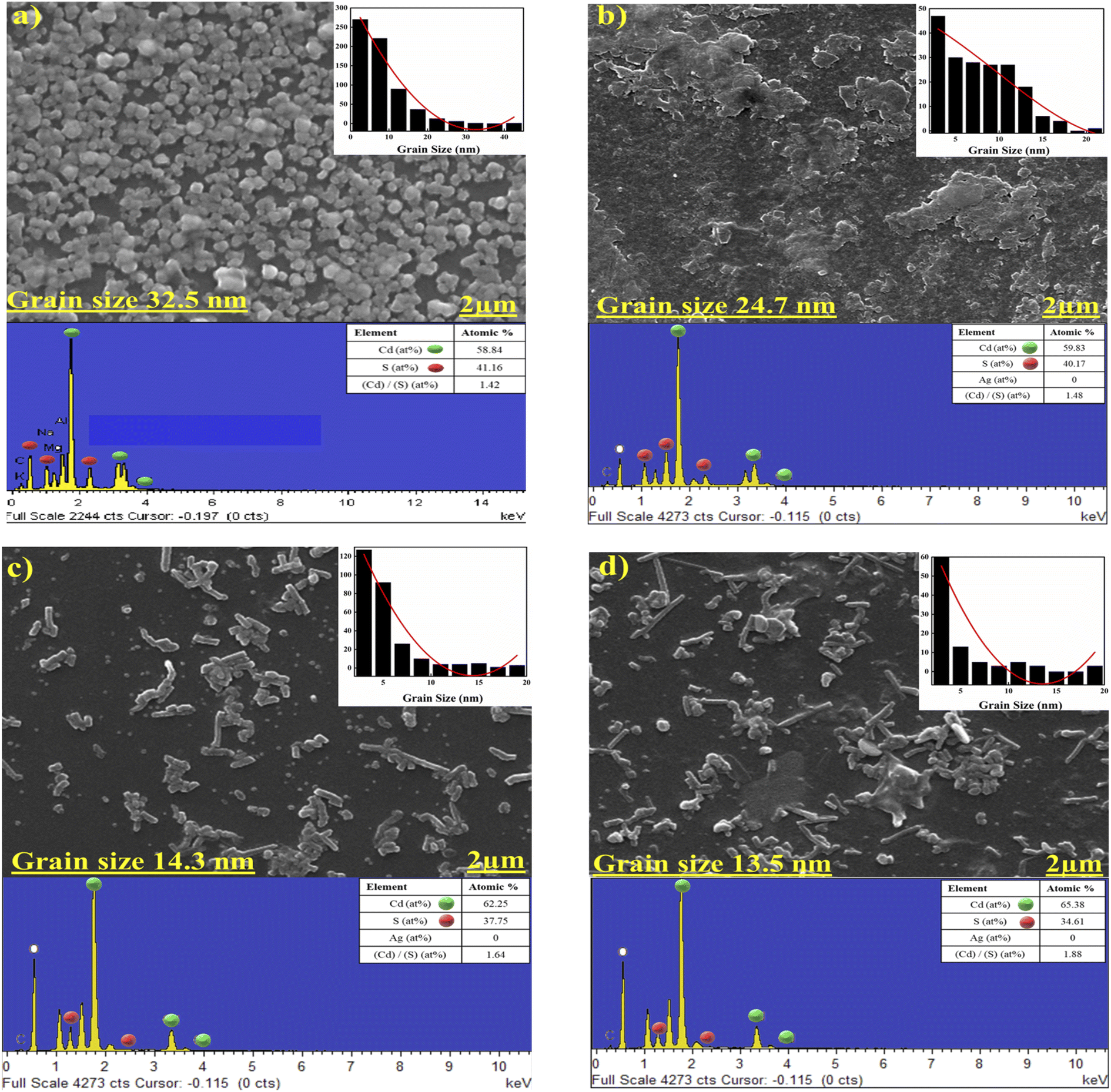 | ||
| Fig. 7 FESEM images with EDX spectra as; (a, b, c and d) for basic CdS, CdS:Ag 1%, CdS:Ag 5%, and CdS:Ag 10%. | ||
FESEM images confirm that Ag-doping has a major impact on the morphology of CdS film, the granular structures of CdS seem to be randomly distributed along the substrate. And there is no uniformity, which led to a tendency to agglomerate with each other to form clusters with many voids, which might be due to the lack of reactivity. This could be attributed to the ionic radius difference between Ag dopant and Cd. Once Ag is introduced to CdS thin film, it can be integrated into the CdS lattice and thus the morphology of CdS film has changed. The heterogeneous growth dynamics of Ag-doped CdS depend on the concentration of doping in solution. However, the electronic properties of doped CdS are related to the actual content of Ag particles.
Fig. 7(b–d) display the FESEM micrographs of CdS:Ag films with different percentage of Ag dopant. A non-uniform distribution of particles and non-densely packed structures is observed in all three samples prepared with varying doping ratios, which indicates that the component crystals grow particularly poorly and have a low crystallinity. The Scherer formula, for instance, is useful for estimating the diffraction profile, and although they can all approximate the exact value of crystallite size, they cannot be compared. XRD determines the size of crystalline domains, while FESEM reveals the physical grains. A single grain may include many domains with various orientations. Consequently, the size measured by FESEM will either be bigger than the size predicted by XRD or, in the case of perfect grains, equal to it. Therefore, grain size measured by FESEM is an average value, while crystallite size is determined using the Scherrer method utilizing diffraction data from a single plane at specific 2θ and FWHM. For basic CdS and CdS + Ag 10%, the grain size decreased from (34.4 to 13.3) nm, respectively. It has been observed that when the Ag ion concentration rises from 1% to 5%, the voids between the CdS particles gets increased and uniform deposition of CdS is minimized. The number of particles increases slightly as 10% of Ag is deposited on the CdS, and with sufficient adhesion of material particles, the surface becomes denser. Adhesion has a crucial part in the growth of thin films, which has a direct effect on power conversion efficiency. The uniform distribution of Ag dopant in between the nanoparticles on the surface of CdS may contribute to uninterrupted passing of electron transport to the back contact of the conducting ITO glass plates and correspondingly result in a substantially improved charge carrier density for electron conduction.
EDX analysis was used to find out the purity and exact chemical composition of both undoped and Ag-doped CdS thin films. This showed that Cd and S are the basic elements, and that the substrate is the source of the other peaks. The typical EDX spectra of each case with the quantitative atomic percentage of the compositional elements have been shown in Fig. 6. From the XRD and EDX results, Ag 1% properly does not include in the Cd–S matrix. Although the XRD results indicate that Ag atoms are replacing Cd atoms substitutional in CdS lattice when the ratio is changed from Ag 1% to Ag 5% and Ag 10% doping but did not detect in EDX, probably due to that even after increasing Ag quantity it is not enough to appear in EDX. It is worth noting, the Cd/S ratio changes significantly for Ag 1% to 10% doping. It shows that for high doping, Ag atoms enter more at interstitial sites than at substitution sites.
Electrical measurements
To improve the device design and thermal stability of microelectronic components, it is essential to have a fundamental understanding of the impact of annealing on the electrical and optical properties of the host material.32 The presence of a large density of localized states with high activation energy is a popular factor in all nano-crystalline semiconducting materials. The electrical conductivity studies of these nano-crystalline materials are important both, the point of view of application and for the analysis of the mobility gap of these materials in localized states. Since CdS thin film is used as a buffer layer, the high conductivity value of CdS film helps to effectively separate the generated charge carriers through the conversion of photovoltaic energy and hence improves the solar cell's performance.33The influence of air annealing on the electrical properties is also well discussed in correlation to film structural alterations. Thus, to study the maximum significant changes that might be happened in the material properties, the air annealing temperature has been selected to be from 150 °C to 450 °C with 10 minutes as annealing time. By matching with Akbarnejad et al., 2017, who choose the variation of annealing temperature between 300 °C to 500 °C.34 In all cases, the n-type conducting nature of CdS thin films was confirmed by the existence of Hall coefficient negative values. The electrical characteristics of chemically deposited CdS, with and without Ag doping, is involving the carrier concentration, mobility, and resistivity. The findings showed that both carrier concentration and mobility are found to improve with a decrease in resistivity when the CdS films are doped with Ag during deposition. Hall measurements of the CdS film showed that the Hall coefficient is negative, which indicates that the CdS films are n-type, Fig. 8(a–c).
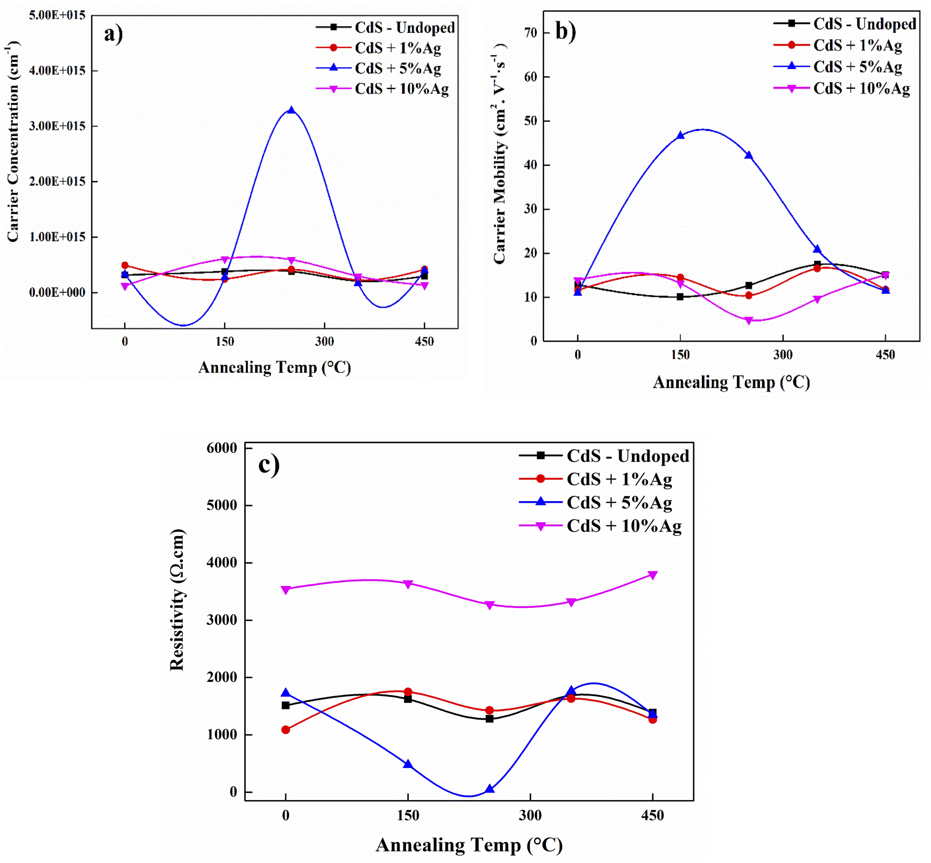 | ||
| Fig. 8 The electrical properties of undoped CdS and Ag-doped CdS films; (a) carrier concentration, (b) carrier mobility, (c) resistivity. | ||
The X-ray diffraction patterns also display the presence of effective Ag-doped by shifting diffraction angle. Due to the introduction of Ag concentration into CdS lattice, the enhancement in electrical properties after Ag doping can be clarified by considering the increase in Cd and Ag vacancies. In the CdS matrix, the Ag vacancies associated with the Cd and S vacancies result in the creation of photosensitization centers. Since the Cd and S vacancy sensitization centers are found in the untreated films because of the lattice defects, the rise in photosensitivity in the film may be due to the formation after doping of additional Ag vacancies in the films. Further increase of Ag concentration ratio led to deteriorate the electrical properties with a particularly drastic degradation at 10% Ag. The resistivity is changing from 1513.46 Ω.cm as deposited without doping to 1088.25 Ω cm with 1% Ag, while sever increased to reach 3543.93 Ω cm at 10% Ag. This is because of two possible reasons, first, the concentration of traps resulting from crystal defects and increasing with doping dominates the concentration of the carrier above a critical silver content. Therefore, when the concentration of Ag has risen, silver atoms serve as traps instead of donors. Secondly, it is attributed to the saturated concentrations of the free carrier and potential declines in mobility due to the formation of Cd–Ag complexes that induce a rise in resistance.35 This may have been induced by the formation of AgxCd(1−x)S complex rather than the doping effect. XRD confirm this explanation through appearing Ag2S with CdS structure. A related finding was previously recorded by Lee et al. (2003) on CdTe/CdS heterojunction solar cells utilizing Boron (B)-doped CdS films prepared with different B concentrations by the CBD technique. The usage of 1 mol% Br for doping CdS films increased the efficiency parameters of the cells (e.g., JSC and FF), but 10 mol% Br decreased the performance of the cells.36
The enhanced conductivity of the films can be associated at annealing temperatures with the enhanced crystallinity of the material. Due to grain growth, the higher conductivity after annealing could be linked to the chemisorbed oxygen at the grain boundaries of the film. As oxygen diffuses through the substance due to the temperature, it integrates to create a conductive CdO with Cd vacancies resulting from lattice defects or thermal breakdown of CdS. Impurities such as oxygen are known to influence the band structure of films by the creation of both trapping and recombination centers. The photo-response of the films under illumination is defined by this balance between trapping and recombination centers. Furthermore, because of the annealing conditions, the dramatic change in resistivity at 450 °C suggests the probability of a change in the structure of the film and composition owing to oxidation. It is evident that films at 5% Ag doping exhibit lower resistivity and higher carrier concentration with little change in terms of mobility, compared with the other doping samples and with the untreated film. As a consequence, it can be deduced that these studies support the general characteristic of photoconductors that the predominance of recombination centers is correlated with a decline in photosensitivity.
Mechanism
Researchers have studied the CBD method for preparing CdS in an alkaline medium. Complexing agents liberate hydroxyl ions from water to control ion precipitation (cadmium and sulphur ions). The CBD method can deposit thin films depending on the type of precursor material, its concentration, the bath temperature, the time of deposition, the solubility equilibrium, the pH of the solution, the stirrer speed, and the substrate.37,38 When all the precursor solutions are mixed, cadmium and sulphur ions react, and the solution turns yellow, indicating CdS synthesis. Cadmium and sulphur ions are slowly and evenly released and deposited on the substrate in an aqueous alkaline bath solution,39,40 forming adherent and uniform CdS thin films. Combining a complexing agent (ligand) with Cd salt creates a cadmium complex that releases Cd2+ ions. Ammonium hydroxide aqueous solution as a complexing agent.41 It prevents the coordination of thiourea's nitrogen atoms with Cd2+ ions and maintains the balance with Cd(OH)2 complex.42Ammonia molecules interact with cadmium ions Cd2+ to form stable quaternary complexes [Cd(NH3)4]2+, which dissociate when sulphur ions S2− are added to the reaction medium.43–45 Cd(II) has four 5s and 5p empty orbitals. When four ammonia molecules interact with cadmium ions, their orbitals hybridise to give sp3 hybridization, resulting in [Cd(NH3)4]2+ complexes' tetrahedral geometry. Electronic displacement from 4d to 5p orbitals hybridised to form [Cd(NH3)4]2+ square planar complexes. Combining orbits (dsp2 hybridization) reduces electrons' electric repulsion (4d orbital). Negatively charged sulphur S2− ions attack the positively charged ionic nucleus of Cd2+ complexes [Cd(NH3)4]2+ and replace ammonia ligands. With the given information, reaction mechanisms can be predicted. First, in the reaction solution, three expected reactions occurred. Third, is the CdS film growth mechanism. Fig. 9 shows homogeneous and heterogeneous nucleation in reaction solutions.
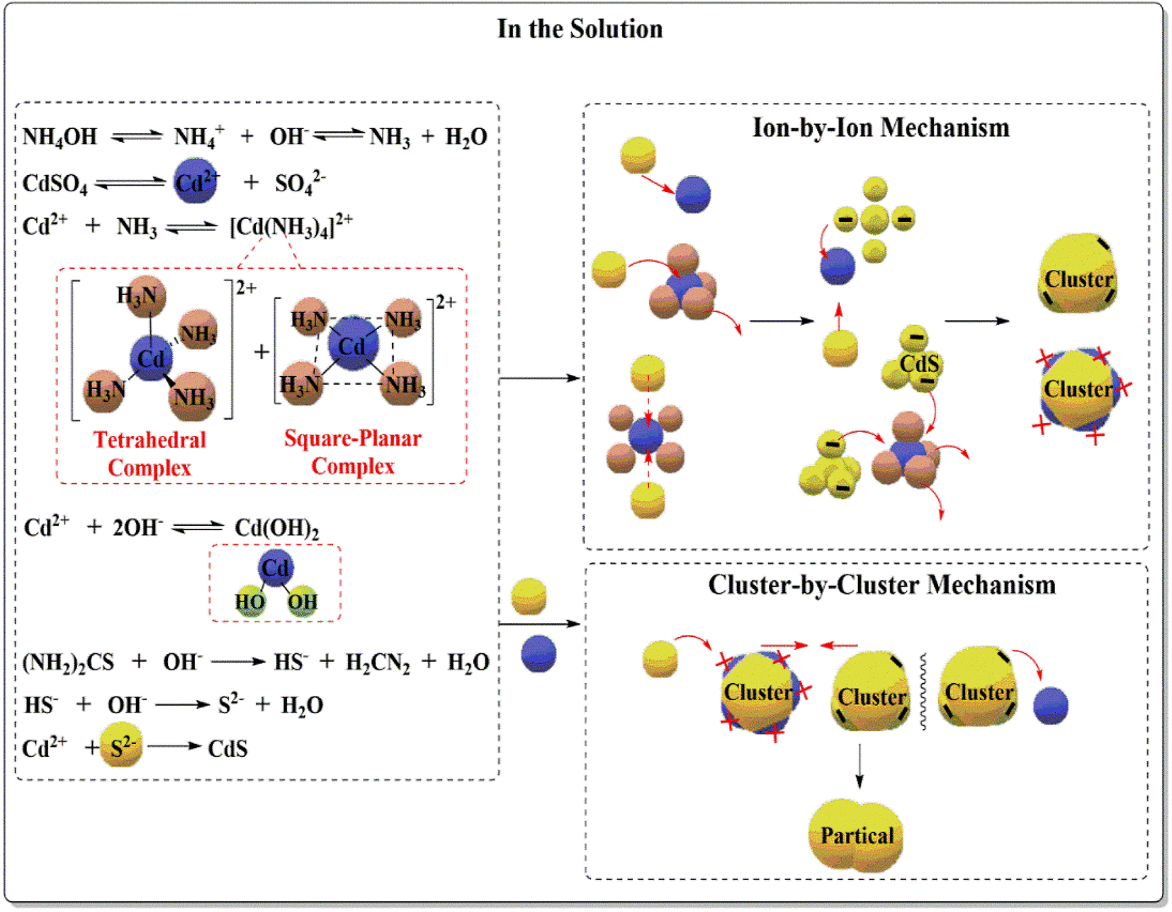 | ||
| Fig. 9 The mechanism of CdS formation in reaction solution. | ||
The collisional interaction of free cadmium ions and sulphur led to the formation of the ion-by-ion mechanism, but most of the cadmium ions were converted to [Cd(NH3)4]2+ complexes or adsorbed by the substrate before adding thiourea to the reaction mixture. Primary CdS molecules interact with [Cd(NH3)4]2+ complexes, forming a cluster. The cluster-by-cluster mechanism governs these collisions. The cluster-by-cluster mechanism is largely responsible for the formation, nature, and shape of the CdS film. Heterogeneous nucleation occurs when cadmium or sulphur ions interact with [Cd(NH3)4]2+ complexes or CdS clusters. [Cd(NH3)4]2+ complexes with CdS clusters also interacted with gather. Lowering electrostatic repulsion between these molecules and CdS cluster surfaces aids nucleation. As the cluster's positive charge increases, the attraction between the negatively charged sulphur ions increases, and their repulsion decrease.
The second proposed mechanism starts on the substrate surface, as shown in Fig. 10. The ends of the soda-lime glass substrate SiO2 contain hydroxyl groups (–OH), which are attracted to the surrounding materials via hydrogen bonds formed with polarised ions and negative ions, as well as electrostatic forces of the oxygen atom.46
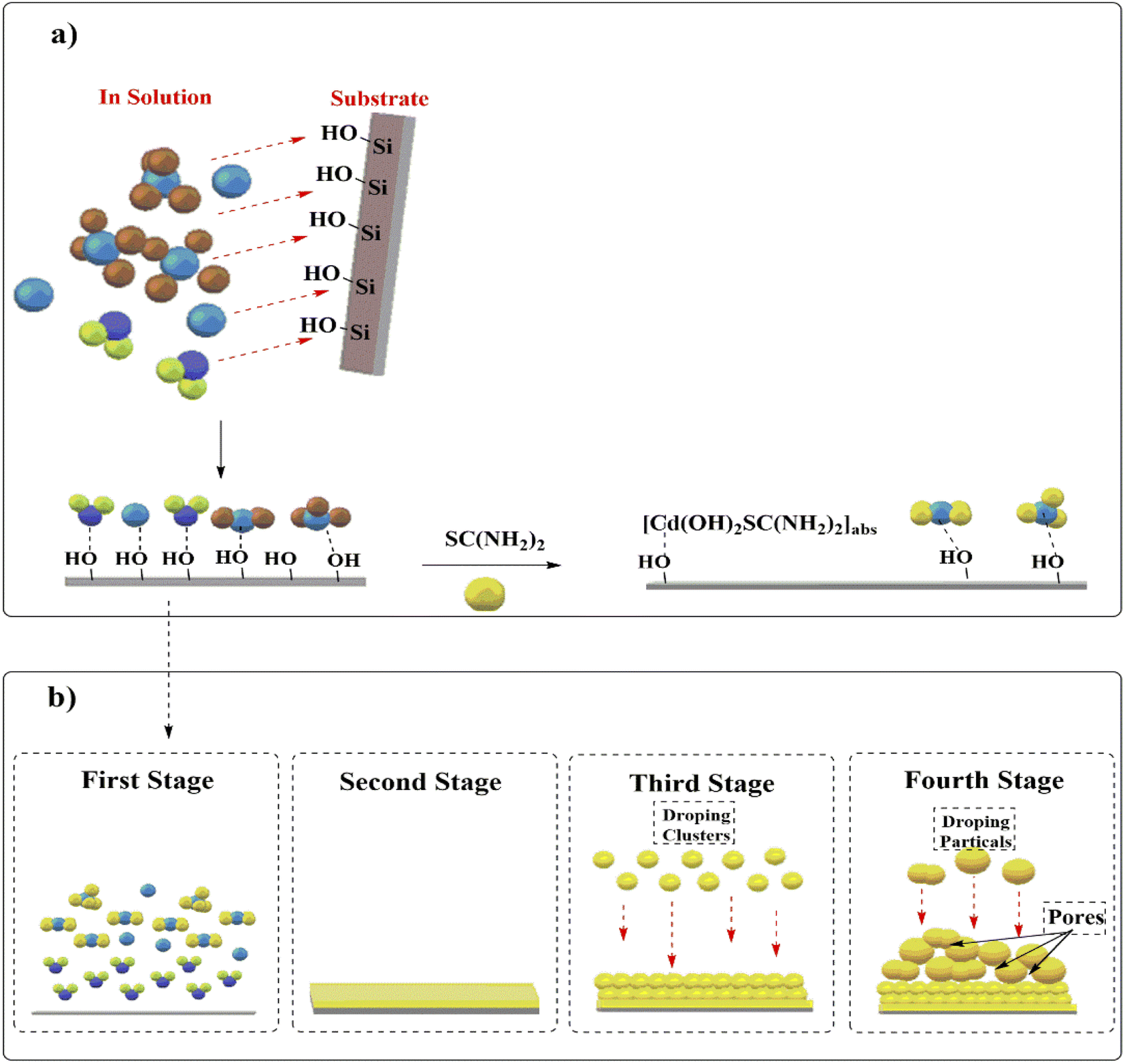 | ||
| Fig. 10 Mechanism of CdS (a) deposition and (b) growth on substrate. | ||
Adsorption of free cadmium ions in the reaction solution occurs first, followed by Cd(OH)2 complexes formed from the first dissociation of ammonium hydroxyl, where oxygen atoms (in –OH groups) on substrate attract free cadmium ions and Cd(OH)2 complexes ((OH)2Cd-OH-Site).47 [Cd(NH3)4]2+. Electrostatic forces between the oxygen atom and the cadmium ion in [Cd(NH3)4]2+ form square-planar and tetrahedral complexes. In comparison to [Cd(NH3)4]2+ tetrahedral complexes, [Cd(NH3)4]2+ square-planar complexes have higher adsorption due to lower steric hindrance.48 To adsorb on a substrate [(NH3)4Cd]2+–OH-Site, the tetrahedral complex must replace one ammonia group with a hydroxyl group. After adding thiourea, a portion of it combines with Cd(OH)2ads complexes to form [Cd(OH)2SC(NH2)2]ads, which are attached to the substrate. This new intermediate dissociates into CdS.49
The CdS film growth mechanism describes the layer formation of CdS film. It has four stages.43,50 Both stages involve synthesis by the reactants. Reactant attraction, repulsion, and collisions prepare the substrate's surface and solution. At this stage, CdS molecules grow compactly and coherently to form the film's initial layers. These layers have low-porosity layers with regularly arranged molecules. It forms from cadmium and sulphur ions and intermediate compounds. During this growth phase, only the primary molecules (CdS, Cd(OH)2[Cd(NH3)4]2+, and [Cd(OH)2SC(NH2)2]ads) and reactants are in their ionic states; their lifetimes for these stages are short. Before they form clusters and particles, they need reactants (ions and molecules in solution). Porosity layer growth occurs in stages 3 and 4. These two stages (3 and 4) have a long life due to increased solution density and mass repulsion from continuous reactions. Third-stage CdS layers form when reaction solution clusters agglomerate and adhere to initial CdS layers. Their adhesion is determined by the relative abundance of the initial CdS layers' general surface charge (whether they have more Cd2+ than S2−, or vice versa) versus the cluster surface charge. Uneven cluster distribution on initial CdS layers increases porosity. This stage focuses on the CdS film's surface topography and morphology and has high adhesion to these layers. In the fourth stage, weak, porous layers' form and can be removed by sonication or mechanical rubbing.
Doping involves adding impurity atoms to semiconductor crystals, which creates an extra energy level near the conduction or valence band edges. Doping semiconductors with acceptors or donors reduced electrical resistivity.4 Doping involves adding a specified volume of a salt solution containing doping atoms to the reaction solution during crystal growth without affecting the crystal lattice structure. In fact, Ag+ ions can help form n-type materials with mostly electron carriers. In our work, we used different concentrations of Ag, which caused a change in the data for samples with an increasing gradient of silver ions based on doping sample analyses. Because the d10 configuration lacks stereo-chemical directionality and silver(I)–ligand interactions are weak, silver ions favour a linear structural geometry.51 Linear geometry with stable excited state energies was the most stable geometrical structure.52,53 In this case, Ag+ donated an electron to Cd2+. As a result of the charge transition from Ag+ ions to Cd complexes, the [Cd(NH3)4]2+ complexes (with a square planar geometry) were transformed into the [Cd(NH3)4]+ complex (with a tetrahedral), resulting in the formation of unstable [Ag(NH3)2]2+ linear complexes. The electron transition from Ag+ to Cd2+ or square-planar [Cd(NH3)4]2+ intermediate complexes changes the shape and charge of cadmium ions. The 4d electrons destroyed [Cd(NH3)4]2+ square-planar's structure. The linear shape of [Ag(NH3)2]+ molecules allowed them to interact with [Cd(NH3)4]2+ complexes and transfer electrons Fig. 11.
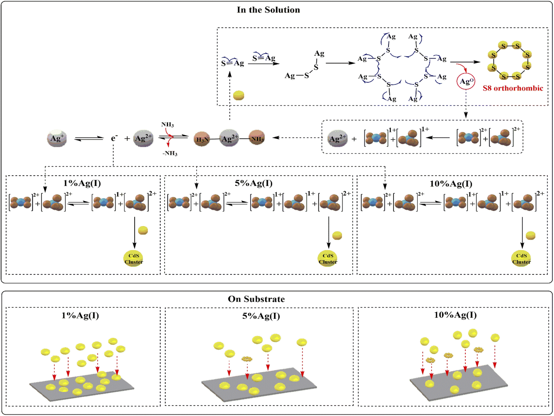 | ||
| Fig. 11 Mechanism of CdS formation doping with different ratios of Ag(I) ions (1, 5, and 10%) in the solution and on the substrates. | ||
Cd(II) cations form more stable complexes with NH3 ligands than Cd(I) cations.54 Ag(II) quickly absorbs a single electron from the reaction medium, reducing it to Ag(I). Experiments showed that S8-orthorhombic XRD patterns emerge at concentrations above 1%.
Silver increases electronic transmission to cadmium intermediate complexes with increasing Ag(I) ion concentration. When 10 and 5% silver is added, cadmium surrounds the silver ions. The electronic transition from silver to cadmium continues with 10% Ag+ ions until thiourea is added. Thiourea forms orthorhombic structures that block silver ions.55 S8 orthorhombic has a crown-like structure, with all atoms forming a single di-sulphide bond using 3py, 3pz electrons.56 Thiol ions SH− and S2− are released in cadmium-equivalent amounts (and containing silver ions). Silver is 2+ and ready to accept a single electron from SH− thiol ions and S2− sulfur in solution. Cd(I) ions are repelled by the electronic density of sulphur ions, preventing them from forming CdS. Ag(II) ions in the reaction mixture solution coordinated with sulphur ions (HS−) (S2−). Because Ag(II) complexes were unstable, thiol groups and/or sulphur ions (S2−) could easily dissociate and release radical mono-anions Sn−.57 These radical mono-anions (Sn−) can form S8 orthorhombic crystals.
A CdS mixture forms within the CdS film's crystal lattice during the basic CdS preparation reaction. The XRD spectrum showed that the CdS film is a mixture of cubic and hexagonal shapes. CdS film's reaction mechanism favors cubes. [Cd(NH3)4]2+ tetrahedral complexes form the hexagonal shape, while square-planar and tetrahedral intermediate complexes form the cubic shape. The reaction mixture can form 1:3 tetrahedral:square-planar complexes. The crystal lattice of CdS film has a 2.5:1.5 cubic:hexagonal geometry ratio. XRD analysis shows that the proposed doping mechanism with silver Ag+ ions is similar at all concentrations. When 1% Ag+ ions are added, the XRD pattern shifts towards hexagonal CdS because the amount of silver Ag+ added is proportional to the amount of square-planar [Cd(NH3)4]2+ complexes formed in the solution. Silver ions easily transfer a single electron to planar square complexes through direct contact with Cd2+. Tetrahedral complexes are slower because of the NH3 ligand. Cubic CdS film will decrease while hexagonal CdS film will increase. The XRD instrument has trouble detecting low concentrations, as its detection limit is 0.5%.58 At 5% and 10% concentration, the CdS-specific pattern changes, with small peaks and a S8 orthorhombic peak at 20.2°. The CdS pattern will shift to the cubic shape at the expense of the hexagonal due to the proposed ratio of intermediate complexes produced from [Cd(NH3)4]2+, as an increase in silver ion concentration will induce the induction of silver ions to provide electrons to tetrahedral [Cd(NH3)4]2+ complexes. The transition occurs through the NH3 ligand due to the difficulty of [Cd(NH3)4]+ complexes interacting with sulphur ions in solution. S8-orthorhombic molecules increase the crystal phase inside the CdS film, and the FWHM of the XRD spectrum narrows with concentration.
FE-SEM images show that adding silver ions to the reaction mixture reduces CdS film deposition on the substrate. The optical properties analysis revealed a decrease in absorption with increasing silver concentration, due to a decrease in CdS deposition on the substrate surface. The ratio of 5% after annealing improved mobility and carrier concentration at 150 °C and 250 °C, as the unreacted thiourea compound decomposed, allowing S8 orthorhombic molecules to regulate electron density flow path within the CdS film's crystal lattice, while reducing resistance caused by electrons travelling.59
Conclusion
In this study, a simple chemical bath deposition approach for depositing Ag-doped CdS films has been described. The impact of doping on the optical, structural, morphological, and electrical characteristics of CdS thin film was discussed and analyzed. The results showed that, the controlling of the reaction mechanism is important, as the change in the concentration of silver led to a change in most of the reaction properties and mechanisms responsible for the formation of the final product. It was found that by reducing the cadmium ions, the doping with silver dopant were able to block the reaction and prevent it from completing. Moreover, when the concentration of silver ions is increased to 5 and 10%, the percentage of precipitate on the substrate decreases due to an increase in the blocking effect caused by the oxidation and reduction reactions. XRD analysis showed that, when the Ag doping concentrations has been increased, more of Ag2+ has been incorporated into the CdS lattice, contributing to the formulation of new composite. Also, optical characterization has revealed that the transparency of the film affected by Ag ratio, causing variation of bandgap from 2.10 to 2.43 eV. Surface morphology shown that grains were randomly orientated on the surface while it was more compact without doping. Furthermore, the improvement in the electrical conductivity of the Ag 5% doped CdS films which exhibited the highest carrier concentration (3.28 × 1015 cm−3) and lowest resistivity (45.2 Ω cm) was taken in advantage to recommended to be a promising candidate as a buffer layer in photovoltaic solar cell.Conflicts of interest
The authors declare that they have no known competing financial interests or personal relationships that could have appeared to influence the work reported in this paper.Acknowledgements
The authors duly acknowledge the contribution of The National University of Malaysia.References
- A. S. Najm, N. Ahmad Ludin, I. Jaber, N. H. Hamid and H. Salah Naeem, Influence of the concentration of chenodeoxycholic acid on the performance of the N719 dye, Inorg. Chim. Acta, 2022, 533, 120776 CrossRef CAS.
- A. M. Holi, A. A. Al-Zahrani, A. S. Najm, P. Chelvanathan and N. Amin, PbS/CdS/ZnO Nanowire Arrays: Synthesis, Structural, Optical, Electrical, and Photoelectrochemical Properties, Chem. Phys. Lett., 2020, 750, 137486 CrossRef CAS.
- Z. R. Abdulghani, A. S. Najm, A. M. Holi, A. A. Al-Zahrani, K. S. Al-Zahrani and H. Moria, Numerical simulation of quantum dots as a buffer layer in CIGS solar cells: a comparative study, Sci. Rep., 2022, 12(1), 1–16 CrossRef PubMed.
- F. J. Willars-Rodríguez, I. R. Chávez-Urbiola, M. A. H. Landaverde, P. Vorobiev, R. R. Bon and Y. V. Vorobiev, Effects of tin-doping on cadmium sulfide (CdS:Sn) thin-films grown by light-assisted chemical bath deposition process for solar photovoltaic cel, Thin Solid Films, 2018, 653, 341–349 CrossRef.
- N. Maticiuc, J. Hiie, T. Raadik, A. Graf and A. Gavrilov, The role of Cl in the chemical bath on the properties of CdS thin films, Thin Solid Films, 2013, 535, 184–187 CrossRef CAS.
- S. Chandramohan, A. Kanjilal, S. N. Sarangi, S. Majumder and R. Sathyamoorthy, Implantation-assisted Co-doped CdS thin films: structural, optical, and vibrational properties, J. Appl. Phys., 2009, 106, 063506 CrossRef.
- P. J. Sebastian, p-type CdS thin films formed by in situ Cu doping in the chemical bath p-type CdS thin films formed by in suit Cu doping in the chemical bath, Appl. Phys. Lett., 1993, 62(23), 2956–2958 CrossRef CAS.
- O. Portillo-Moreno, et al., Growth of CdS:Cu Nanocrystals by Chemical Synthesis, J. Electrochem. Soc., 2006, 153(10), 926–930 CrossRef.
- Y. Sánchez, M. Neuschitzer, M. Dimitrievska and E. Saucedo, High VOC Cu2ZnSnSe4/CdS:Cu based solar cell: evidences of a Metal-Insulator-Semiconductor (MIS) type hetero-junction, IEEE 40th Photovolt. Spec. Conf., vol. 8, 2014, pp. 0417–0420 Search PubMed.
- K. K. Challa, E. Magnone and E. T. Kim, Highly photosensitive properties of CdS thin films doped with boron in high doping levels, Mater. Lett., 2012, 85, 135–137 CrossRef CAS.
- H. Khallaf, G. Chai, O. Lupan, L. Chow, S. Park and A. Schulte, Investigation of aluminium and indium in situ doping of chemical bath deposited CdS thin films, J. Phys. D: Appl. Phys., 2008, 41(18), 185304 CrossRef.
- H. Khallaf, et al., In situ boron doping of chemical-bath deposited CdS thin films, Phys. Status Solidi A, 2009, 206(2), 256–262 CrossRef CAS.
- H. Khallaf, G. Chai, O. Lupan, L. Chow, S. Park and A. Schulte, Characterization of gallium-doped CdS thin films grown by chemical bath deposition, Appl. Surf. Sci., 2009, 255(Nov), 4129–4134 CrossRef CAS.
- A. Salh, et al., Effect of Gallium doping on CdS thin film properties and corresponding Cu(InGa)Se2/CdS:Ga solar cell performance, Thin Solid Films, 2018, 660, 207–212 CrossRef.
- S. Chandel, P. R. Ajan, A. J. Vallamattom, V. P. N. Nampoori and P. Radhakrishnan, A Study of CdS and Ag doped CdS Prepared through CBD Technique, International Conference on Fibre Optics and Photonics, 2012, pp. 6–8 Search PubMed.
- V. S. Taur, R. A. Joshi and R. Sharma, Annealing-Induced Modifications in Physicochemical and Optoelectronic Properties of Ag-Doped Nanostructured CdS Thin Films, Int. J. Photoenergy, 2012, 1–7 CrossRef.
- S. R. Ferrá-González, et al., Optical and structural properties of CdS thin films grown by chemical bath deposition doped with Ag by ion exchange, Optik, 2014, 125(4), 1533–1536 CrossRef.
- A. Flores-Pacheco, et al., Stimulation of the photoluminescent properties of CBD-CdS thin films achieved by structural modifications resulting from Ag+ doping, Phys. Status Solidi RRL, 2017, 11(8), 2–5 Search PubMed.
- F. J. Willars-Rodríguez, I. R. Chávez-Urbiola, R. Ramírez-Bon, P. Vorobiev and Y. V. Vorobiev, Effects of aluminum doping in CdS thin films prepared by CBD and the performance on Schottky diodes TCO/CdS:Al/C, J. Alloys Compd., 2019, 817, 152740 CrossRef.
- A. S. Najm, H. S. Naeem, K. O. Alabboodi and S. A. Hasbullah, New systematic study approach of green synthesis CdS thin film via Salvia dye, Sci. Rep., 2022, 12(1), 1–21 CrossRef PubMed.
- S. A. Jassim, A. A. Rashid, A. Zumaila, G. Abdella and A. Al, Influence of substrate temperature on the structural, optical and electrical properties of CdS thin films deposited by thermal evaporation q, Results Phys., 2013, 3, 173–178 CrossRef.
- A. S. Najm, H. Moria and N. A. Ludin, Areca catechu as photovoltaic sensitizer for dye-sensitized solar cell (DSSC), Biointerface Res. Appl. Chem., 2020, 10(3), 5636–5639 CAS.
- M. Rehman, A. Maqsood and M. Shafique, Properties of Cu-doped ZnTe thin films prepared by closed space sublimation (CSS) techniques, J. Mater. Sci., 2003, 39(3), 1101–1103 Search PubMed.
- A. S. Najm, et al., Effect of Chenodeoxycholic Acid on the Performance of Dye-sensitized Solar Cells utilizing Pinang Palm (Areca catechu) Dye, Sains Malays., 2020, 49(12), 2971–2982 Search PubMed.
- S. Ebrahimi and B. Yarmand, Optimized optical band gap energy and Urbach tail of Cr2S3 thin films by Sn incorporation for optoelectronic applications, Phys. Rev. B, 2020, 593, 2020 Search PubMed.
- A. S. Najm, et al., Impact Of Cadmium Salt Concentration On Cds Nanoparticles Synthesized By Chemical Precipitation Method, Chalcogenide Lett., 2020, 17(11), 537–547 CAS.
- S. Ikhmayies and R. N. Ahmad-bitar, Temperature dependence of the photoluminescence spectra of CdS:In thin films prepared by the spray pyrolysis technique, J. Lumin., 2013, 142, 40–47 CrossRef CAS.
- A. S. Hassanien and A. A. Akl, Effect of Se addition on optical and electrical properties of chalcogenide CdSSe thin films Superlattices and Microstructures Effect of Se addition on optical and electrical properties of chalcogenide CdSSe thin films, Superlattices Microstruct., 2016, 89, 153–169 CrossRef CAS.
- S. S. Chiad, W. A. Jabbar and N. Habubi, Effects of Annealing on the Electronic Transitions of ZnS Thin Films, J. Arkansas Acad. Sci., 2011, 65(1), 39–42 CAS.
- M. F. Abdullah, et al., Impact of the TiO2 nanosolution concentration on heat transfer enhancement of the twin impingement jet of a heated aluminum plate, Micromachines, 2019, 10(3), 1–22 Search PubMed.
- N. Azmi, et al., A comprehensive study on the effects of alternative sulphur precursor on the material properties of chemical bath deposited CdS thin films, Ceram. Int., 2020, 46, 18716–18724 CrossRef CAS.
- M. S. Jamal, et al., Effects of growth temperature on the photovoltaic properties of RF sputtered undoped NiO thin films, Results Phys., 2019, 14, 102360 CrossRef.
- A. S. Najm, P. Chelvanathan, S. K. Tiong and M. T. Ferdaous, Numerical Insights into the Influence of Electrical Properties of n-CdS Buffer Layer on the Performance of SLG/Mo/p-Absorber/n-CdS/n-ZnO/Ag Configured Thin Film Photovoltaic Devices, Coating, 2021, 11(1), 1–17 Search PubMed.
- E. Akbarnejad, Z. Ghorannevis, F. Abbasi and M. Ghoranneviss, Investigation of annealing temperature effect on magnetron sputtered cadmium sulfide thin film properties, J. Theor. Appl. Phys., 2017, 11(1), 45–49 CrossRef.
- K. E. Nieto-zepeda, A. Guillén-cervantes, K. Rodríguez-rosales, J. Santos-cruz and D. Santos-cruz, Effect of the sulfur and fluorine concentration on physical properties of CdS films grown by chemical bath deposition, Results Phys., 2017, 7, 1971–1975 CrossRef.
- J. Lee, J. Yi, K. Yang, J. Park and R. Oh, Electrical and optical properties of boron doped CdS thin films prepared by chemical bath deposition, Thin Solid Films, 2003, 432(3), 344–348 CrossRef.
- U. G. Substrate, S. Sublimation, N. Amin and M. R. Karim, Impact of CdCl2 Treatment in CdTe Thin Film Grown on Ultra-Thin Glass Substrate via Close Spaced Sublimation, Crystals, 2021, 11(4), 390 CrossRef.
- A. Al Qassem, Effect of heat treatment in presence of CdCl2 on the physical properties of pCdTe/nCdS heterojunction solar cells, Facultatea de Ştiinţe Exacte, 2016, 7(7), 166–169 Search PubMed.
- A. A. G. Regmi, A. R. Núñez, M. S. López and H. Castaneda, Comparative studies of CdS thin films by chemical bath deposition techniques as a buffer layer for solar cell applications, J. Mater. Sci.: Mater. Electron., 2020, 14, 1–20 Search PubMed.
- X. Zhou, Z. Li, Z. Li and S. Xu, Preparation and formation mechanism of CdS nano-films via chemical bath deposition, Front. Chem., 2008, 3(1), 18–22 Search PubMed.
- C. K. Kumar, et al., Highly Photoconductive CdS Thin Films Synthesized by UsingChemical Bath Deposition, J. Korean Phys. Soc., 2009, 55(1), 284–287 CrossRef CAS.
- F. Tyholdt, Chemical Solution Deposition of Thin Films, 2005 Search PubMed.
- C. H. Choi, B. K. Paul and C. H. Chang, Microreactor-assisted solution deposition for compound semiconductor thin films, Processes, 2014, 2(2), 441–465 CrossRef.
- P. Kundu, P. A. Deshpande, G. Madras and N. Ravishankar, Nanoscale ZnO/CdS heterostructures with engineered interfaces for high photocatalytic activity under solar radiation, J. Mater. Chem., 2011, 21(12), 4209–4216 RSC.
- X. H. Fan, H. J. Liu, Y. M. Chen and T. Sun, Synthesis and characterization of CdS nanoparticles, Adv. Mater. Res., 2014, 848(1), 3–6 Search PubMed.
- D. Camuffo, Thermodynamics for cultural heritage, Phys. Methods Archaeom., 2004, 154, 37–98 Search PubMed.
- R. Ortega-Borges and D. Lincot, Mechanism of Chemical Bath Deposition of Cadmium Sulfide Thin Films in the Ammonia – Thiourea System : In Situ Kinetic Study and Modelization, J. Electrochem. Soc., 1993, 140(12), 3464–3473 CrossRef CAS.
- Q. Nie, Q. Yuan, W. Chen and Z. Xu, Effects of coordination agents on the morphology of CdS nanocrystallites synthesized by the hydrothermal method, J. Cryst. Growth, 2004, 265(3–4), 420–424 CrossRef CAS.
- N. S. Kozhevnikova, A. S. Vorokh and A. A. Uritskaya, Cadmium sulfide nanoparticles prepared by chemical bath deposition, Russ. Chem. Rev., 2015, 84(3), 225–250 CrossRef.
- C. Voss, S. Subramanian and S. O. Ryu, Growth Kinetics of Thin-Film Cadmium Sulfide by Ammonia-Thiourea Based CBD, J. Electrochem. Soc., 2014, 151(10), 8–13 Search PubMed.
- M. A. Haj, C. B. Aakero and J. Desper, Silver(I) coordination chemistry: from 1-D chains to molecular rectangles, New J. Chem., 2013, 37(1), 204–211 RSC.
- P. Danwanichakul, T. Suwatthanarak, C. Suwanvisith and D. Danwanichakul, The Role of Ammonia in Synthesis of Silver Nanoparticles in Skim Natural Rubber Latex, J. Nanosci., 2016, 1–6 Search PubMed.
- V. Dubois, P. Archirel, P. Maıtre and L. D. C. Physique, Theoretical study of the rearrangement of AgzNH3/2 after electronic excitation . Comparison with NazNH3/2, Chem. Phys. Lett., 2000, 323(1–2), 1–6 CrossRef CAS.
- S. Muthaiah, A. Bhatia and M. Kannan, Stability of Metal Complexes, in Stability and Applications of Coordination Compounds represented, 2020. pp. 1–18 Search PubMed.
- M. M. Ikuriya, et al., Crystal Structure of S8 Molecule from Thiourea, Cryst. Struct. Commun., 2020, 36, 8–9 Search PubMed.
- R. Steudel and Y. Steudel, Polysulfide chemistry in sodium-sulfur batteries and related systems – a computational study by G3X(MP2) and PCM calculations, Chem.–Eur. J., 2013, 19(9), 3162–3176 CrossRef CAS PubMed.
- R. Steudel and T. Chivers, The role of polysulfide dianions and radical anions in the chemical, physical and biological sciences, including sulfur-based batteries, Chem. Soc. Rev., 2019, 48(12), 3279–3319 RSC.
- J. A. Newman, et al., Parts per Million Powder X-Ray Diffraction, Anal. Chem., 2015, 87(21), 10950–10955 CrossRef CAS PubMed.
- G. Abbady, A. Qasem and A. M. Abd-elnaiem, Optical parameters and electronic properties for the transition of the amorphous-crystalline phase in Ge20Te80 thin films, J. Alloys Compd., 2020, 842, 155705 CrossRef CAS.
| This journal is © The Royal Society of Chemistry 2022 |