DOI:
10.1039/D2RA04602D
(Paper)
RSC Adv., 2022,
12, 31180-31185
Polymers based on thieno[3,4-c]pyrrole-4,6-dione and pyromellitic diimide by CH–CH arylation reaction for high-performance thin-film transistors†
Received
24th July 2022
, Accepted 24th October 2022
First published on 1st November 2022
Abstract
Three homopolymers were successfully synthesized by direct CH–CH arylation polymerization of thieno[3,4-c]pyrrole-4,6-dione or pyromellitic diimide derivatives affording highly purified polymers with high molecular weights (43.0–174.7 K). Thieno[3,4-c]pyrrole-4,6-dione and pyromellitic diimide derivatives are considered as electron-withdrawing units. The synthesized homopolymers P1, P2, and P3 showed band gaps in the range of 2.13–2.08 eV, respectively. The electron mobilities of the three homopolymers have been investigated. The thin film transistor for P1 prepared by the eutectic-melt-assisted nanoimprinting method achieved an electron mobility of 2.11 × 10⁻³ cm2 s−1 V−1. Based on the obtained results, the synthesized polymers can be used as potential electron acceptors in solar cell applications.
Introduction
Several synthetic methodologies including electrochemical,1–3 chemical oxidative4–6 and transition metal-catalyzed cross-coupling reactions7–10 have been investigated for the synthesis of π-conjugated organic and polymeric materials. Direct C–H arylation reaction has been proved to be a particularly efficient methodology for the formation of carbon–carbon bonds without the use of organometallic nucleophiles.11–22 Direct arylation reactions have been reported by many researchers including our group,15–22 and proven to be useful for synthesizing a variety of π-conjugated polymers with high molecular weights. In the past decade, comprehensive efforts have been made on transition metal (e.g., Pd and Fe) catalysed oxidative coupling on arenes.23–25 Very recently, transition metal-free oxidation acylation of arenes has shown a promising method for oxidative acylation of different heteroarenes.26,27 Oxidative coupling of C–H bonds without prior functionalization is an environmentally friendly, step-economically, and sustainable method.28–30
During the last decade, the performance of organic thin-film transistors (OTFT) has advanced dramatically with the charge carrier mobility (μ) and now approaching 100 cm2 V−1 s−1.31,32 While there are a variety of p-type organic semiconductors, n-type materials are relatively limited. PCBM has been widely used as an acceptor owing to its excellent electron-accepting and electron-transporting properties.33,34 However, PCBM has relatively low absorption in the visible and near-IR. The use of acceptor polymers with improved light absorption has met with limited success.35,36 To improve OTFT applications, other n-type acceptors with suitable properties such as high absorption and high oxidation resistance are still highly demanded.37 In addition, to enhance optical and electrical properties, many groups have tried to improve organic semiconductors' crystallinity with a controlled crystal structure. However, the highly crystalline polymers has low solubility which will hamper device fabrication by using the conventional methods. Therefore, in this paper, the eutectic-melt-assisted nanoimprinting (EMAN) method was applied to fabricate optoelectronic devices based on highly crystalline polymers instead of solution casting techniques.38 Nanoimprinting technique is one of the most convenient production processes because of its advantages such as cost-effective, scalable production and obtained high-resolution structures, etc.39
Herein, we wish to report on the Pd(II)-catalyzed regioselective direct CH–CH arylation coupling reaction for the synthesis of some polymers based on thieno[3,4-c]pyrrole-4,6-dione and pyromellitic diimide with high molecular weights (43.0–174.7 K), which can be used as n-type semiconducting materials. The direct heteroarylation polycondensation reaction provides an environmentally friendly and fast route with minimal reaction steps.40–44 The catalytic CH–CH direct arylation coupling of two heteroarenes represents a promising advance in organic chemistry and the synthesis of small molecules.45,46 Dimethylformamide (DMF) was essentially used as a reaction solvent as it has been proved particularly to be effective for obtaining high catalytic activity.47,48 In addition, the electron mobility of the homopolymer P1-based FET device has successfully been fabricated by the eutectic-melt-assisted nanoimprinting (EMAN) method49,50 and its thin-film transistor has achieved electron mobility is 2.11 × 10⁻³ cm2 V−1 s−1.
Experimental
Instruments and measurements
All manipulations and reactions involving air-sensitive reagents were performed under a dry oxygen-free nitrogen atmosphere. All 1H- and 13C-NMR spectra were measured on a Varian spectrometer (400 MHz for 1H-NMR and 100 MHz for 13C-NMR) in CDCl3 at 25 °C with TMS as the internal standard. Chemical shifts were recorded in ppm units. The gel permission chromatography (GPC) analysis was conducted with Shimadzu (LC-20A prominence Series) instrument. Chloroform was used as a carrier solvent (flow rate: 1 ml min−1 at 40 °C) and calibration curves were made with standard polystyrene samples.
Materials
All reagents and solvents were obtained from commercial sources and dried using standard procedures before use. Pyromellitic acid diimide, palladium acetate, and potassium acetate were obtained from Sigma-Aldrich. Tetrabutylammonium bromide (TBAB) was obtained from TCI Company. Thiophene-3,4-dicarboxylic acid was obtained from Matrix Scientific. All reactions were monitored by TLC to follow their completion.
General procedure for the synthesis of homopolymers P1, P2 and P3
Under a nitrogen atmosphere, potassium acetate (2.26 mmol), tetrabutylammonium bromide (0.75 mmol), and palladium acetate (0.037 mmol) were added to a stirred solution of starting material (0.37 mmol) in anhydrous DMF (7 ml). The resulting suspension was heated under reflux for 48 h at 120 °C. The reaction mixture was cooled to room temperature and then poured into methanol. The crude polymer was collected via filtration and washed successively with methanol. The residual solid was loaded into an extraction thimble and washed repeatedly with methanol (48 h), hexane (48 h), followed by acetone (48 h) followed by drying under vacuum affording the desired polymer. For more details, see ESI.†
General fabrication of FET devices
FET devices were fabricated by the eutectic-melt-assisted nanoimprinting (EMAN) method.49–54 Briefly, the powder mixtures of each polymer (P1, P2, and P3) and 1,4-DBTFB (polymer = 2 wt%) were first placed on a substrate and covered with a PDMS mask. The sample was then heated to melt the powder completely. At this time, the molten liquid was sucked into the grooves of the PDMS mold by the capillary force. The extra liquid was removed by soaking out using paper. The sample was cooled down to room temperature. After removing the PDMS mold, the sample was placed in a vacuum to remove 1,4-DBTFB. The resulting polymer wires were transferred on a highly doped p-type silicon wafer (100) with a thermally grown 200 nm thick oxide layer using a liquid-bridge-mediated nano transfer molding (LB-nTM) method.49 By using LB-nTM, the laterally aligned P1 wires can be transferred to the hydrophilic SiO2 substrate. Finally, 200 nm thick gold electrodes separated by 100 μm were vacuum deposited through a shadow mask on the P1 wire patterns. Current–voltage (I–V) characteristics of the devices were measured using bottom-gate FET geometry under the ambient conditions at room temperature, and the saturation regime mobility was calculated. FET devices based on P2 and P3 did not properly work due to poor film morphology or poor adhesion property.
Results and discussion
Synthesis of homopolymers P1, P2 and P3
The synthesis of some π-conjugated homopolymers and their electron mobilities properties have been investigated. Thieno[3,4-c]pyrrole-4,6-dione derivatives with electron-withdrawing groups having good arrangement and planarity have been used. We successfully synthesized some homopolymers in a few steps, at low cost, and with good charge mobility. 5-Hexyl-thieno[3,4-c]pyrrole-4,6-dione (HTPD), 5-(2-ethylhexyl)thieno[3,4-c]pyrrole-4,6-dione (ETPD) and 1,5-di(2-ethylhexyl)-pyromellitic diimide (EPDI) were selected to be used for the synthesizing the target homopolymers. All the homopolymers were synthesized by CH–CH arylation polymerization (Scheme 1).
 |
| | Scheme 1 Synthesis of the polymers by CH–CH arylation polymerization. | |
In CH–CH arylation polymerization, the unsubstituted positions which are highly reactive by the presence of electron-withdrawing and/or electron-donating group can be activated by the catalyst in the presence of a highly polar solvent such as DMF, DMAC, or DMSO to start the polymerization giving a high molecular weight polymer in good yield. For instance, polymer P1 could be obtained with a high yield (70%) and a high molecular weight (Mn = 174 K). The polymer P2 was also successfully prepared by the same CH–CH arylation method with lower yield (50%) and lower molecular weight (Mn = 70.5 K) when compared to those corresponding values obtained for polymer P1. This is probably due to the effect of the branched alkyl chain which reduces the planarity of the polymer despite the presence of the imide group which makes the 3,4-positions on thiophene ring very active. Furthermore, EPDI derivative could also be polymerized under the present methodology of CH–CH arylation conditions affording the desired homopolymer P3 with a yield of 49% and Mn value of 43.0 K (PDI = 1.5). Interestingly, polymer P3 showed lower Mn values when compared to is less than P1 in the Mn because the reactivity of the thiophene ring is higher than the benzene ring so this affected gradually the reactivity of the unsubstituted 4,9 positions on the benzene ring in EPDI. The optimized condition for all the polymers and their high molecular weights and PDI are shown in Table 1. However, the molecular weights and PDI values were measured by gel permission chromatography (GPC).
Table 1 Chemical yields and GPC data for the synthesis of π-conjugated homopolymersa
| Entry |
Polymer |
Mn,b (kDa) |
PDI (Mw/Mn)b |
Yieldc (%) |
| All polymers were prepared via CH–CH arylation in presence of Pd(OAc)2 (10 mol%) as a catalyst in DMF at 120 °C for 48 h. GPC calibration based on polystyrene standards using CHCl3 as the mobile phase, Mn = number average molecular weight, PDI = polydispersity index. Based on the weight of pure polymers obtained after Soxhlet extraction followed by drying under vacuum for 24 h. |
| 1 |
P1 |
174.7 |
1.3 |
70 |
| 2 |
P2 |
70.5 |
1.2 |
50 |
| 3 |
P3 |
43.0 |
1.5 |
49 |
Optical and electrochemical properties of homopolymers P1, P2 and P3
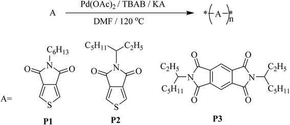
The optical properties of homopolymers P1, P2 and P3 were investigated by UV-vis absorption spectroscopy for both solution and thin films (Fig. 1). As shown in Fig. 1, the polymers P1, P2 and P3 show similar absorption UV-vis spectra with narrow absorption at short wavelengths, giving almost similar optical bandgaps. P3 shows λonset in the solid-state is ∼593.5 nm, which is ∼10 nm red-shifted compared to that of P1 (∼581 nm) and P2 (∼580 nm). In comparison to the optical properties of the synthesized polymers and PCBM, we find that they are similar to PCBM optical properties which were published earlier.55 All the absorption spectra of P1, P2 and P3 show bandgaps in the range 2.13–2.08 eV similar to PCBM too.
 |
| | Fig. 1 UV-vis absorption spectra of P1, P2 and P3 (a) in solution and (b) as casted film. Chloroform was used as the solvent. | |
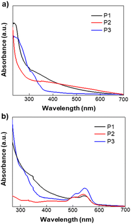
Cyclic voltammetry (CV) measurement was performed on potentiostat/galvanostat (SP-150 OMA Company). The supporting electrolyte was tetrabutylammonium hexafluorophosphate (TBAPF6) in acetonitrile (0.1 M) at a scan rate 50 mV s−1. A three-electrode cell was used and Pt wire and Ag/AgCl [Ag in 0.1 M KCl] were used as the counter and reference electrodes, respectively. The (EHOMO and ELUMO) of the homopolymers were determined from the following relationships: EHOMO = −(Eoxd + 4.72) eV and ELUMO = −(Ered + 4.72) eV. Where Eoxd and Ered are the onset oxidation and reduction potentials of the polymers vs. the Ag/AgCl reference electrode, respectively. The polymer films were drop-casted from polymer–chloroform solution on ITO glass slides, ca. 10 mg ml−1. The voltammograms of polymers P1, P2, and P3 versus SCE are shown in Fig. 2. Energy levels were estimated using the onset of the reduction peak (LUMO level) and the onset of the oxidation peak (HOMO level), assuming that the SCE is −4.72 eV from the vacuum. The results obtained are summarized in Table S2.† Energy levels of polymers P1, P2 and P3 are relatively low with LUMO energy levels in the range of −3.72 to −3.89 eV, a value that is close to that of PC61BM. The LUMO energy level of polymer P1 was found to be at −3.74 eV. HOMO energy levels are also low with a value of −5.64 and −5.61 eV for both P1 and P2 and −5.64 eV for P3. However, these three polymers show no electrochemical reversibility in the oxidation and reduction processes.
 |
| | Fig. 2 Cyclic voltammograms of homopolymers P1, P2, and P3 measured in a 0.1 M solution of TBAPF6 in acetonitrile at a scan rate of 50 mV s−1. | |
XRD study of homopolymers P1, P2 and P3
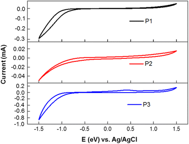
The X-ray diffraction (XRD) of the homopolymers P1–P3 was measured from their thin-film casting on the silicon substrate (Fig. 3). All polymers did not show any peaks in the narrow-angle region, which indicates there is no arrangement of the alkyl chain in the solid state. The diffraction peaks at 2θ = 17.99° (4.98 Å), and 28.01° (3.28 Å) for P1; 18.00° (4.98 Å), and 28.01° (3.28 Å) for P2; and 27.31° (3.39 Å) for P3 are attributed to π–π stacking between polymer chains. The XRD results implied that all the polymers possess a good arrangement in the solid state because of the π–π stacking between the polymer units. The differences in the peak intensities between these polymers indicate that the crystallinity in the solid-state is related to the backbone and alkyl substitutions of the backbone, which will affect the uniformity of film and the device performance.
 |
| | Fig. 3 X-ray diffraction (XRD) patterns of P1, P2 and P3. Films for XRD measurement were prepared by drop casting in CHCl3 (10 mg ml−1 of solvent) on the silicon substrate. | |
Field-effect mobility study of homopolymer P1, P2, and P3
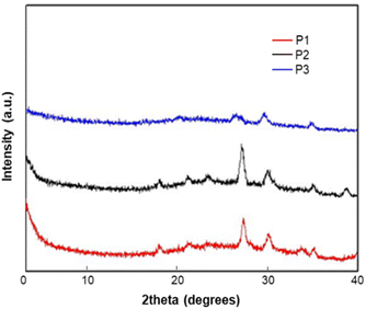
The field-effect mobility of P1 was investigated. Due to the rigid planarity, P1 has low solubility in most common organic solvents which hamper the fabrication of FET devices by using conventional processes. As addressing this issue, the eutectic-melt-assisted nanoimprinting (EMAN)49–54 method was applied to create FET devices using polymer P1. Briefly, wire patterns of P1 with 1.5 μm/3.0 μm line and space were first created by EMAN (Fig. 4), and then they were transferred on a highly doped silicon wafer with a thermally grown 200 nm thick oxide layer. Subsequently, 200 nm thick gold electrodes separated by 100 μm were deposited through a showdown mask on the wire patterns. Current–voltage (I–V) characteristics of the fabricated FET devices were measured using bottom-gate geometry, and the saturation regime mobility was calculated. As shown in Fig. 5, the transfer and output curves of polymer P1 show n-type characteristics. Similar to other n-type semiconductors, a large hysteresis was observed.56–58 The calculated saturation electron mobility is 2.11 × 10⁻³ cm2 s−1 V−1, which is comparable to the electron mobility of PC61BM.59,60 FET devices based on polymer P2 and P3 were also prepared by EMAN. Because of poor film morphology or poor adhesion problem (ESI Fig. S10 and S11†), both P2 and P3-based FET devices didn't successfully work.
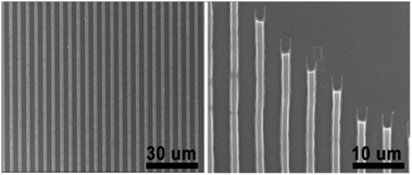 |
| | Fig. 4 SEM image of the wire patterns of P1 created by EMAN. | |
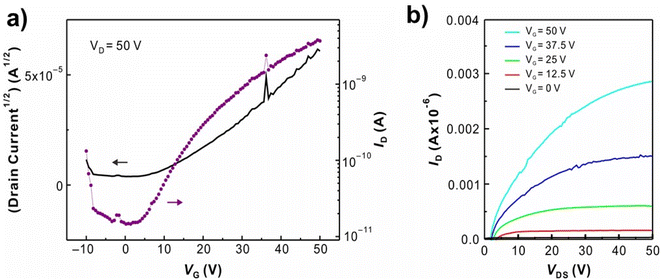 |
| | Fig. 5 Representative (a) transfer and (b) output curves of FET device using P1 show electron mobility of 2.11 × 10⁻³ cm2 s−1 V−1. | |
Conclusions
We have successfully synthesized homopolymers P1, P2 and P3 presenting n-type properties for potential applications as acceptor polymers. The homopolymers were synthesized using the CH–CH arylation polymerization in an eco-friendly one-step coupling reaction which reduces the number of steps necessary to obtain these polymers, respectively. These polymers possess low lying HOMO and LUMO levels. Also, their electron mobilities were tested and the resulting electron mobility was as high as 2.11 × 10⁻³ cm2 s−1 V−1 which is comparable to that of PCBM. These polymers are promising features for applications as acceptors in all-polymer solar cells and transistors and will be further investigated in the future.
Author contributions
G. M. Nassar: conceptualization, methodology, formal analysis, investigation, visualization, writing – original draft, review & editing. J. Chung: methodology, formal analysis, investigation, writing – review & editing. C. K. Trinh: formal analysis, investigation, writing – review & editing. A. A. El-Shehawy: writing – review & editing. A. A. El-Barbary: writing – review & editing. Y. Kang: writing – review & editing. Supervisor J.-S. Lee: writing – review & editing, resources, supervision.
Conflicts of interest
There are no conflicts to declare.
Acknowledgements
This research was supported by the Samsung Research Funding Center of Samsung Electronics under Project Number SRFC-MA1502-11. We would like to thank Van Lang University, Vietnam for the support for this research.
Notes and references
- Y. Li, C.-Y. Gao, X.-H. Fan and L.-M. Yang, J. Chem. Eng., 2022, 443, 136536 CrossRef.
- S. Yin, W. Lu, R. Wu, W. Fan, C.-Y. Guo and G. Chen, ACS Appl. Mater. Interfaces, 2020, 12, 3547–3553 CrossRef PubMed.
- C. Fradin, F. Guittard, I. F. Perepichka and T. Darmanin, Electrochim. Acta, 2022, 425, 140684 CrossRef.
- O. A. Kraevaya, A. F. Latypova, A. A. Sokolova, A. A. Seleznyova, N. A. Emelianov, N. A. Slesarenko, V. Y. Markov, L. A. Frolova and P. A. Troshin, Sustainable Energy Fuels, 2022, 6, 3485–3489 RSC.
- L. Papammagri, S. R. Agnihotra, N. Maohar, R. M. Bouldin and S. K. Manohar, Macromolecules, 2021, 54, 1507–1516 CrossRef.
- M. Seike, M. Uda, T. Suzuki, H. Minami, S. Higashimoto, T. Hirai, Y. Nakamura and S. Fujii, ACS Omega, 2022, 15, 13010–13021 CrossRef.
- Y.-Z. Chen, J.-G. Fu, X.-M. Ji, S.-S. Zhang and C.-G. Feng, Chem. Commun., 2022, 58, 6661–6664 RSC.
- C. K Trinh, G. M. Nassar, N. I. Abdo, S. Jung, W. Kim, K. Lee and J.-S. Lee, RSC Adv., 2022, 12, 17682–17688 RSC.
- S. Xu, E. H. Kim, A. Wei and E.-I. Negishi, Sci. Technol. Adv. Mater., 2014, 15, 044201–044223 CrossRef CAS.
- F. Babudri, G. M. Farinola and F. Naso, J. Mater. Chem., 2004, 14, 11–34 RSC.
- T. J. Aldrich, A. S. Dudnik, N. D. Eastham, E. F. Manley, L. X. Chen, R. P. H. Chang, F. S. Melkonyan, A. Facchetti and T. J. Marks, Macromolecules, 2018, 51, 9140–9155 CrossRef CAS.
- Y. Sui, Y. Shi, Y. Deng, R. Li, J. Bai, Z. Wang, Y. Dang, Y. Han, N. Kirby, L. Ye and Y. Geng, Macromolecules, 2020, 53, 10147–10154 CrossRef CAS.
- V. Dichiarante, M. Fagnoni and A. Albini, Angew. Chem., Int. Ed., 2007, 46, 6495–6498 CrossRef CAS PubMed.
- T. Jia, A. Bellomo, S. Montel, M. Zhang, K. EL Baina, B. Zheng and P. J. Walsh, Angew. Chem., Int. Ed., 2014, 53, 260–264 CrossRef PubMed.
- N. I. Abdo, J. Ku, A. A. El-Shehawy, H.-S. Shim, J.-K. Min, A. A. El-Barbary, Y. H. Jang and J.-S. Lee, J. Mater. Chem. A, 2013, 35, 10306–10317 RSC.
- W. Elsawy, H. Kang, K. Yu, A. El-Barbary, K. Lee and J.-S. Lee, J. Polym. Sci., Part A: Polym. Chem., 2014, 52, 2926–2933 CrossRef.
- M. Shaker, J.-H. Lee, C. K. Trinh, W. Kim, K. Lee and J.-S. Lee, RSC Adv., 2015, 5, 66005–66012 RSC.
- M. Shaker, C. K. Trinh, W. Kim, K. Lee and J.-S. Lee, New J. Chem., 2015, 39, 4957–4964 RSC.
- C. K. Trinh, J.-H. Lee, J. Choi, M. Shaker, W. Kim and J.-S. Lee, New J. Chem., 2018, 42, 2557–2563 RSC.
- Y.-S. Yang, S. Lee, S. H. Son, H.-S. Yoo, Y. H. Jang, J.-W. Shin, H.-J. Won, J. Sim and N.-J. Kim, Org. Chem. Front., 2022, 9, 5906–5911 RSC.
- F. D'Amico, C. Papucci, D. Franchi, G. Reginato, M. Calamante, L. Zani, A. Dessì and A. Mordini, ACS Sustainable Chem. Eng., 2022, 10(9), 3037–3047 CrossRef.
- A. Ichige, H. Saito, J. Kuwabara, T. Yasuda, J.-C. Choi and T. Kanbara, Macromolecules, 2018, 51, 6782–6788 CrossRef.
- C. Y. K. Chan, N.-W. Tseng, J. W. Y. Lam, J. Liu, R. T. K. Kwok and B. Z. Tang, Macromolecules, 2013, 46, 3246–3256 CrossRef.
- Y. Yue, J. Peng, D. Wang, Y. Bian, P. Sun and C. Chen, J. Org. Chem., 2017, 82, 5481–5486 CrossRef.
- P.-Y. Lee, P. Liang and W.-Y. Yu, Org. Lett., 2017, 19, 2082–2085 CrossRef.
- S. Rej and N. Chatani, Angew. Chem., Int. Ed., 2022, 61, e202209539–e202209556 CrossRef.
- S. Rej, A. Dasa and N. Chatani, Chem. Sci., 2021, 12, 11447–11454 RSC.
- C. S. Yeung and V. M. Dong, Chem. Rev., 2011, 111, 1215–1292 CrossRef PubMed.
- S. A. Girard, T. Knauber and C.-J. Li, Angew. Chem., Int. Ed., 2014, 53, 74–100 CrossRef PubMed.
- Y. Wu, J. Wang, F. Mao and F. Y. Kwong, Chem.–Asian J., 2014, 9, 26–47 CrossRef PubMed.
- I. Osaka, T. Abe, S. Shinamura, E. Miyazaki and K. Takimiya, J. Am. Chem. Soc., 2010, 132, 5000–5001 CrossRef.
- S. Fratini, M. Nikolka, A. Salleo, G. Schweicher and H. Sirringhaus, Nat. Mater., 2020, 19, 491–502 CrossRef PubMed.
- G. Yu, J. Gao, J. C. Hummelen, F. Wudl and A. J. Heeger, Science, 1995, 270, 1789–1791 CrossRef.
- A. Chaudhary, D. K. Pathak, M. Tanwar, P. Yogi, P. R. Sagdeo and R. Kumar, ACS Appl. Electron. Mater., 2019, 1, 58–63 CrossRef.
- J. J. M. Halls, C. A. Walsh, N. C. Greenham, E. A. Marseglia, R. H. Friend, S. C. Moratti and A. B. Holmes, Nature, 1995, 376, 498–500 CrossRef.
- Y. Kim, S. Cook, S. A. Choulis, J. Nelson, J. R. Durrant and D. D. C. Bradley, Chem. Mater., 2004, 16, 4812–4818 CrossRef.
- M. Liao, J. Duan, P. Peng, J. Zhang and M. Zhou, RSC Adv., 2020, 10, 41764–41779 RSC.
- Y. Jiang, J. Chen, Y. Sun, Q. Li, Z. Cai, J. Li, Y. Guo, W. Hu and Y. Liu, Adv. Mater., 2019, 31, 1805761 CrossRef PubMed.
- J. Ge, B. Ding, S. Hou, M. Luo, D. Nam, H. Duan, H. Gao, Y. C. Lam and H. Li, Nat. Commun., 2021, 12, 3146 CrossRef PubMed.
- L. Ackermann, Chem. Rev., 2011, 111, 1315–1345 CrossRef PubMed.
- T. Satoh and M. Miura, Chem. Lett., 2007, 36, 200–205 CrossRef.
- M. Lafrance and K. Fagnou, J. Am. Chem. Soc., 2006, 128, 16496–16497 CrossRef PubMed.
- N. I. Abdo, A. A. El-Shehawy, A. El-Barbary and J.-S. Lee, Eur. J. Org. Chem., 2012, 28, 5540–5551 CrossRef.
- M. Wakioka, N. Ichihara, Y. Kitano and F. Ozawa, Macromolecules, 2014, 47, 626–631 CrossRef.
- X. Jie, Y. Shang, P. Hu and W. Su, Angew. Chem., Int. Ed., 2013, 52, 3630–3633 CrossRef.
- Y. Yang, J. Lan and J. You, Chem. Rev., 2017, 117, 8787–8863 CrossRef PubMed.
- D. Alberico, M. E. Scott and M. Lautens, Chem. Rev., 2007, 107, 174–238 CrossRef PubMed.
- I. V. Seregin and V. Gevorgyan, Chem. Soc. Rev., 2007, 36, 1173–1193 RSC.
- J. K. Hwang, Nat. Nanotechnol., 2010, 5, 742–748 CrossRef.
- J. Chung, J. Hyon, K.-S. Park, B. Cho, J. Baek, J. Kim, S. U. Lee, M. M. Sung and Y. Kang, Sci. Rep., 2016, 6, 1–11 CrossRef PubMed.
- Q. Zhang, K. D. O. Vigier, S. Royer and F. Jérôme, Chem. Soc. Rev., 2012, 41, 7108–7146 RSC.
- D. Carriazo, M. C. Serrano, M. C. Gutiérrez, M. L. Ferrera and F. d. Monte, Chem. Soc. Rev., 2012, 41, 4996–5014 RSC.
- C. Bathula, S. Jeong, J. Chung and Y. Kang, J. Nanosci. Nanotechnol., 2016, 16, 2796–2799 CrossRef CAS PubMed.
- J. Kim, J. Chung, J. Hyon, T. Kwon, C. Seo, J. Nam and Y. Kang, Chem. Commun., 2014, 50, 10258–10261 RSC.
- S. Cook, H. Ohkita, Y. Kim, J. J. Benson-Smith, D. D. C. Bradley and J. R. Durrant, Chem. Phys. Lett., 2007, 445, 276–280 CrossRef CAS.
- W. Xu and S.-W. Rhee, Org. Electron., 2011, 12, 2040–2046 CrossRef CAS.
- W. Xu and S.-W. Rhee, Org. Electron., 2010, 11, 836–845 CrossRef CAS.
- Y. Ni, Y. Wang and W. Xu, Small, 2021, 17, 1905332 CrossRef CAS PubMed.
- E. V. Hauff, V. Dyakonov and R. Parisi, Sol. Energy Mater. Sol. Cells, 2005, 87, 149–152 CrossRef.
- C. Waldauf, P. Schilinsky, M. Perisutti, J. Hauch and C. J. Brabec, Adv. Mater., 2003, 15, 2084–2088 CrossRef CAS.
|
| This journal is © The Royal Society of Chemistry 2022 |
Click here to see how this site uses Cookies. View our privacy policy here. 
 Open Access Article
 This Open Access Article is licensed under a Creative Commons Attribution-Non Commercial 3.0 Unported Licence
 d,
Ashraf A. El-Shehawye,
Ahmed A. El-Barbary*b,
Youngjong Kang
d,
Ashraf A. El-Shehawye,
Ahmed A. El-Barbary*b,
Youngjong Kang


