
 Open Access Article
 This Open Access Article is licensed under a Creative Commons Attribution-Non Commercial 3.0 Unported Licence
Fabrication of a boron-doped nanocrystalline diamond grown on an WC–Co electrode for degradation of phenol
Tao Zhang *ab,
Zhe Xuec,
Ying Xiea,
Guodong Huanga and
Guangpan Penga
*ab,
Zhe Xuec,
Ying Xiea,
Guodong Huanga and
Guangpan Penga
aMechanical Institute of Technology, Wuxi Institute of Technology, Wuxi 214122, China. E-mail: zhangt@wxit.edu.cn
bSchool of Engineering Science and Technology, Shanghai Ocean University, Shanghai 201316, China
cZhangjiagang Weina New Materials Technology Co., Ltd., Suzhou 201316, China
First published on 20th September 2022
Abstract
Cemented carbide (WC–Co) is applied as the substrate instead of conventional ones such as Si, Ti, and Nb, on which nanocrystalline BDD films are deposited by hot filament chemical vapor deposition. Then the WC–Co/BDD electrodes are investigated by Field Emission Scanning Electron Microscopy (FE-SEM), Micro-Raman Spectroscopy, X-ray photoelectron spectroscopy (XPS), a four-point probe method, accelerated life test (ALT), and electrochemical analysis. According to the results, the BDD films deposited on the WC–Co substrate are highly uniform and pinhole-free with a grain size of 100 nm and a low compressive stress. The WC–Co/BDD electrode has a wide potential window of 3.8 V and low background currents in 0.5 mol L−1 H2SO4 electrolytes and shows a quasi-reversible behavior in the K3[Fe(CN)6] redox system. The electrode has a service life of more than 400 h in the ALT with 3 mol L−1 H2SO4 electrolytes at a constant current density of 1 A cm−2. These electrochemical performances of BDD films on the WC–Co substrate is similar to or even slightly better than that on the commonly used substrates. Finally, phenol is used as a pollutant to test the activity of the WC–Co/BDD electrode. The results of replicated experiments show that the average COD reduces from the initial 5795 to 85 mg L−1, and the average current efficiency is about 46%. This suggests that the WC–Co/BDD electrode has a good mineralization capacity in phenol with a high concentration.
1. Introduction
Refractory organic wastewater occurs mainly in the production processes of the printing and dyeing, chemical, pesticide, pharmaceutical, and other industries. A considerable part of the pollutants in wastewater are a class of highly hazardous substances that are mutagenic, teratogenic or carcinogenic to humans.1–3 These pollutants, such as phenol, cannot be completely removed by conventional biochemical methods (such as biological filtration, activated sludge, and oxidation ponds) due to their non-biodegradable or toxic character.1,4 Therefore, many physical–chemical technologies are emerging to effectively remediate such effluents. Therein, electrochemical oxidation technology has occupied an important place in most areas of science and technology during the past three decades. The technology is applied by strong oxidants (hydroxyl radicals, ˙OH) which are generated from water at an appropriate anode, and the oxidants could mineralize the organic compounds to CO2 and H2O.5–7 The electrochemical oxidation technology has the following core advantages.8–10 (i) Environmental compatibility. The primary reagent that is the hydroxyl radical generated in the process of electrolysis is environment-friendly and effective against pollutants. (ii) Amenability to automation. In general, the related reactor is simple and the process is flexible and controllable, making it easy to control using an automatic system. (iii) Energy efficiency. Technology could remove organic pollutants with a high removal rate at room temperature and atmospheric pressure. However, the energy consumption and efficiency for oxidising the organic pollutant are greatly dependent on the anode electrode materials.There are many research works focused on the fabrication and characterization of various electrode materials, including stainless steel, Pt, graphite, Ti-based oxide anode materials (RuO2, PbO2, IrO2, SnO2, etc.), and boron-doped diamond (BDD). Among them, the BDD films deposited on various heterogeneous substrates by chemical vapor deposition (CVD) method have attracted considerable attention because of their outstanding properties. (i) The BDD films show a wide electrochemical window (about 3.5 V) and high oxygen overpotential, as well as extremely low background current in water and organic solution.11,12 These characteristics make BDD films probably to have desirable catalytic activity and current efficiency while degrading pollutants.13 (ii) The BDD films possess similar excellent physical characteristics to no-doped diamond films, such as high hardness and strong chemical inertness. The BDD electrodes show little degradation on their electrochemical activity with time during the process of oxygen evolution. Also, there is nearly no oxidation or reduction reaction on the surfaces of the electrodes. Therefore, the BDD electrodes have a longer service life compared with other traditional ones.5,14 Moreover, the BDD is reported to show an attractive ability to degrade ammonia nitrogen, phenol, chlorophenol, aniline, dyes, surfactants, alcohols, and many other organic pollutants.15 Therefore, the BDD films have become the most promising commercial electrode material.
The BDD electrodes with a long service life are required to improves the efficiency and reduces the cost of sewage treatment. The service life of BDD electrodes is vitally dependent on the quality of films and the adhesion between coatings and heterogeneous substrates. Meanwhile, the two factors are influenced by the deposition parameters and the difference in thermal expansion coefficients between films and substrates. Therefore, many researchers have been doing continuous exploration on the growth and properties of BDD films with different substrates, such as Si,15,16 refractory metals Nb and Ta,17,18 and Ti.13,14 However, the Si substrate shows low mechanical strength, and the Nb and Ta substrates have unacceptably high costs.5,15,16 The diamond films generally has a low adhesion to the Ti substrate due to the large differences in the thermal expansion coefficient and lattice mismatches between Ti and BDD.19
Cemented carbide is a kind of wear-resistant material commonly used in cutting tools, and it is made of WC hard compound of refractory metal and Co bonded metal. The WC–Co substrate has many excellent properties such as high hardness, wear resistance, and moderate price. Moreover, the difference in the thermal expansion coefficients in WC–Co/BDD is less than that in Nb/BDD or Ta/BDD, or Ti/BDD.20,21 In the past decade, many researchers investigated on the fabrication and application of the no-doped or boron-doped diamond films deposited onto the WC–Co cutting tools. In our previous work, dense no-doped diamond films were synthesized on the as-pretreated surface of WC–Co tools, which have been applied in machining graphite, carbon fiber, high silicon aluminum, and other difficult to machine materials.22,23 It demonstrates that the diamond films show good adhesion and quality onto the WC–Co substrate. Sun and Shen have carried out systematic research on the fabrication and characterization of WC–Co/BDD cutting tools; they pointed out that the addition of boron is conducive to improving the adhesion between diamond films and WC–Co substrate.24,25 Saito et al. also synthesized BDD films on WC–Co with good adhesion and resistance to oxidation.26 Hence, it could be inferred that the cemented carbide is an ideal substrate candidate for BDD electrodes. Nevertheless, to our knowledge, there has been little research on the electrochemical properties of WC–Co/BDD and its removal performances for pollutants.
In this work, BDD coatings are deposited onto a WC–Co substrate by hot filament CVD method. Furthermore, we prepared the nanocrystalline BDD films onto the substrate, instead of the conventional microcrystalline ones, because the nanocrystalline films have higher specific surface area and lower residual stress than the microcrystalline films.16 We investigated the surface morphology, boron concentration, electrochemical window, background current, and reversibility capacity of the WC–Co/BDD electrode. Then an accelerated life test is conducted to explore the electrochemical stability of WC–Co/BDD. Finally, phenol is used as a pollutant to test the activity of the WC–Co/BDD electrodes.
2. Experiments details
2.1 Electrode preparation
A self-made hot filament CVD (HFCVD) is applied to deposit BDD films by a dynamic boron-doping method. Acetone, trimethyl borate (C3H9BO3), and excessive hydrogen are introduced as the reactive source. The trimethyl borate is dissolved in acetone solution according to a preset [B]/[C]gas atomic ratio of 5000 ppm.27 The tantalum wires (Φ 0.5 mm) are used as hot filaments, which are dragged to be straight by thermal stable springs.27 WC–Co (6% Co composition) rods of 3 mm diameter are used as substrates. The substrates are treated by two-step chemical pretreatment, which is first etched with Murakami's reagent for 30 min and then Caro's acid solution for 60 s.22 Subsequently, the samples are abraded using commercial diamond powders with the grain size of 5 μm to cause more surface defects and improve the diamond nucleation density. After that, the substrates are cleaned in ultrasonic bath with deionized water and acetone for 5 min to remove the diamond particles. The nucleation and deposition parameters are shown in Table 1.| Parameters | Nucleation parameters | Growth parameters |
|---|---|---|
| The ratio of CH4 to H2 | 2.0% | 1.5% |
| [B]/[C]gas (ppm) | 5000 | 5000 |
| Pressure (kPa) | 2 | 2 |
| Substrate temperature (°C) | 800 | 850 |
| Filament temperature (°C) | 2000 ± 200 | 2200 ± 200 |
| Duration (min) | 30 | 270 |
2.2 Electrode characterization
The surface morphologies of the pretreated and deposited samples are observed by Field Emission Scanning Electron Microscopy (FE-SEM, Zeiss ULTRA55). The elementary compositions of the as-pretreated sample are detected by EDX. The boron concentration and internal stress of the as-deposited sample is examined by Micro-Raman Spectroscopy (SPEX1403) and X-ray photoelectron spectroscopy (XPS, Escalab 250xi). The resistivity of sample is measured by four-point probe method.The potential window of BDD electrodes is tested by cyclic voltammetric at a scan rate of 0.1 V s−1 in 0.5 mol L−1 H2SO4 solutions. The cyclic voltammograms are collected by CHI 605 electrochemical workstation (CH Instrument, Shanghai, China). A conventional three-electrode cell is adopted (as shown in Fig. 1(a)), with the nanocrystalline WC–Co/BDD as the working electrode (effective area: 1 cm2), a Pt rod as the counter electrode, and an Ag/AgCl as the reference electrode. Meanwhile, the reversibility capacity of BDD electrodes is measured by the various scan rates in 0.1 mol L−1 KCl solutions containing 0.01 mol L−1 KFe(CN)6.
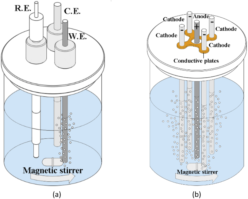 | ||
| Fig. 1 (a) The three-electrode cell scheme used in the cyclic voltammetric and linear sweep voltammetric. (b) The electrochemical reactor scheme used in the accelerated life and pollutant oxidation tests; the WC–Co/BDD electrode is designated as the anode; the four WC–Co rods are used as the cathodes, which are connected by a copper conductive plate. The target solutions are stirred by a magnetic stirrer. | ||
2.3 Accelerated life and pollutant oxidation tests
Accelerated life test (ALT) is performed in 250 mL, 3 mol L−1 H2SO4 solutions at room temperature. A constant current power supply is used to provide the stable current density of 1 A cm−2. The parameters in the ALT are set depending on the commonly used ones in the BDD coatings with the conventional substrates.14,28 The WC–Co/BDD is served as the anode with an effective area of 1 cm2, which is surrounded by four WC–Co rods used as the cathodes (as shown in Fig. 1(b)). The distance between the anode and each cathode is fixed at 10 mm. The target solution is continuously mixed and stirred by a magnetic bar throughout the test. During the experiments, the potential of the anode is monitored.Phenol is adopted as the target object, which is reported to be one of the most toxic organic pollutants presenting in the discharge of various industrial effluents.29 The target solution consists of phenol and 0.5 mol L−1 H2SO4, in which the phenol concentration is 0, 0.5, 1, 3, 10, 25 mmol L−1, respectively. 25 mmol L−1 phenol solution is prepared by dissolving 2.35 g of C6H5OH (∼99%) in distilled water and diluting to 1000 mL, and then the solution is diluted to 0.5, 1, 3, and 10 mmol L−1 of phenol, respectively. The target solutions are tested by linear sweep voltammetric using the three-electrode cell at a scan rate of 0.1 V s−1, in order to investigate the oxidation potential of phenol for WC–Co/BDD electrode. The electrodes are set the same as those provided in the cyclic voltammetric tests (as shown in Fig. 1(a)). Subsequently, the solution with a high concentration of phenol (25 mmol L−1) is degraded using a constant current power supply which is used to provide the stable current density of 100 mA cm−2. Besides, the anode and cathode arrangements are shown in Fig. 1(b). The chemical oxygen demand (COD) test is commonly used to measure the amount of organic compounds in wastewater, measured by a visible spectrophotometer with a wavelength of 420 nm (LH-C660, Lohand, China).
3. Results and discussion
3.1 Physical characterization
The pretreatment on WC–Co substrate plays a decisive role in the quality of diamond films and adhesive strength between the films and WC–Co. The presence of Co-based binder could suppress the diamond nucleation and promote the growth of an intermediate graphitic layer, resulting in poor adhesion of the coatings to substrate ultimately.22,30 The pretreatment focuses on removing the Co element and creating defect sites on the surfaces of substrate. Fig. 2(a) shows the surface morphologies of the WC–Co samples pretreated by the chemical and abrading process. There are some tiny holes on the surface of the substrate because the cobalt binder has been removed. The cobalt content on the as-pretreated surfaces is about 0.16 wt%, which is measured by EDX and presented in Fig. 2(b). It has been proved that when the cobalt content is around or less than 0.2%, the films show a strong adhesion to the WC–Co substrate in our previous works.22 After the 5 hours deposition process, the dense nanocrystalline boron-doped diamond films are deposited onto the substrate and the thickness of the films is about 4 μm, as shown in Fig. 2(c) and (d). The films are highly uniform and pinhole-free with the grain size of around 100 nm. It should be noted that the relatively low reactive pressure of 2000 Pa is maintained to improve the nucleation density and secondary nucleation during the nucleation and growth process of the films. The low-pressure leads to an increased mean free path of active species, which results in decreasing collisions of the species during their transport to the substrate and increasing the concentration of nucleating species eventually.31,32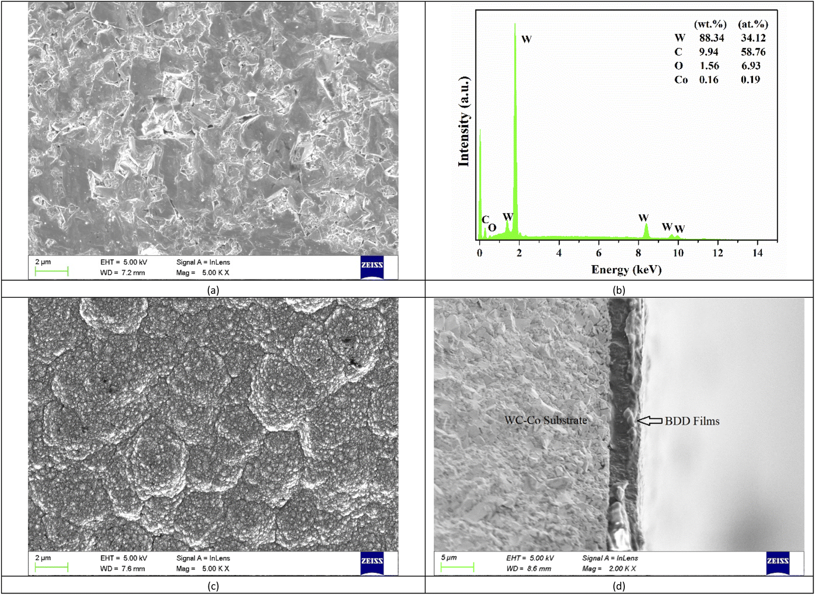 | ||
| Fig. 2 (a) Surface morphology and (b) element content analysis of as-pretreated WC–Co sample; (c) top view and (d) cross section of as-deposited nanocrystalline BDD coatings on the WC–Co substrate by FESEM. | ||
The WC–Co/BDD electrode is evaluated by Raman spectroscopy using He–Ne laser with an excitation wavelength of 532 nm, as exhibited in Fig. 3. The Raman curve is fitted with Lorentzian function and then six primary peaks are observed. A sharp peak at 1336 cm−1 corresponding to sp3 bonding of the diamond can be observed, which moves to a high-frequency direction relative to the bulk diamond's characteristic peak of 1332 cm−1. The residual stress of films is calculated according to the following equation:33
| σ = −0.567(vm − v0) (GPa) |
| [B] (cm−3) = 8.44 × 1030 × exp(−0.048 × ω500) |
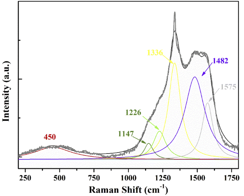 | ||
| Fig. 3 Typical Raman spectra of as-deposited nanocrystalline BDD films on the WC–Co substrate, which is fitted by Lorentzian function. | ||
Fig. 4 represents the XPS spectra of the WC–Co/BDD sample decomposed by the asymmetrical Gaussian/Lorentzian mixed function. The results show that the boron concentration of the sample is 1.5 at% (approximately 2.6 × 1021 cm−3), which is slightly lower than the value calculated by the Raman method. The B1s spectrum with a low signal-to-noise ratio can be fitted roughly by two bands, as shown in Fig. 4(a). Here, a peak at 188.3 ± 0.125 eV is assigned to a bond of boron with carbon (B4C); another peak at 192.7 eV is assigned to a bond of boron with oxygen.38 In addition, the C1s spectrum gives three components (as shown in Fig. 4(b)). A peak at 284.7 eV that is a usual position for carbon atoms of diamond lattice presents in the heavily boron doped polycrystalline diamond films.39 A peak at 284.2 keV is attributed to a covalent carbon–carbon bonds adjacent to substituting boron atoms.39 The component around 286 eV is ascribed to ether (C–O–C), which is also reported as the main component on the surface of heavily boron doped polycrystalline films.40
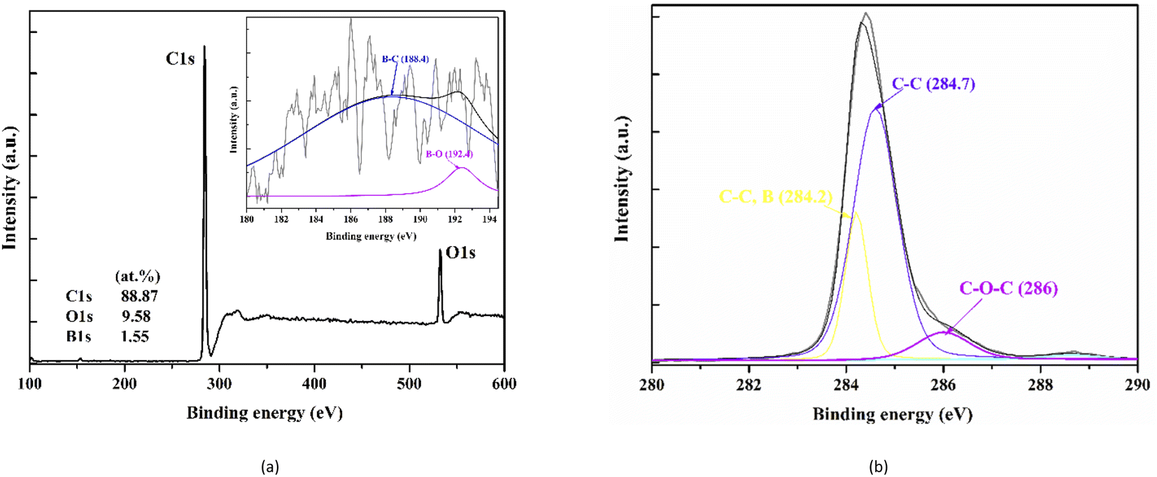 | ||
| Fig. 4 (a) Typical XPS of as-deposited nanocrystalline BDD films on the WC–Co substrate and B1s; (b) XPS of C1s. | ||
The WC–Co substrate and the WC–Co/BDD electrode are examined for their resistivity by four-point probe method. The resistivity value of WC–Co sample is 0.03 mΩ cm and that of as-deposited sample is 0.2 mΩ cm. At the similar boron concentration in the films around 1021 cm−3, Si/BDD has a large resistivity around 104 to 106 mΩ cm,37 and Nb/BDD and Ti/BDD have a low resistivity around 10−2 to 10 mΩ cm.28,41 Obviously, the nanocrystalline WC–Co/BDD electrode, like Nb/BDD and Ti/BDD, have a high electrical conductivity, and thus could be applied in the electrochemical oxidation for the degradation of the pollutants.
3.2 Cyclic voltammetric behavior
The typical cyclic voltammograms of WC–Co/BDD electrode obtained in the 0.5 mol L−1 H2SO4 solutions are presented in Fig. 5(a). The potential is swept between −2.0 V and 3.5 V vs. Ag/AgCl. It can be detected the relatively large voltammetric current and O2 evolution current in the first few scanning cycles. The voltammetric current gradually decreases with increasing potential cycles until it stabilizes after 5 cycles, due to the electrochemical “etching” or surface cleaning effect. In fact, the graphite and amorphous carbon impurities on the surface of BDD films are likely to react to form CO and/or CO2 during the potential cycling, which could decrease the electrochemically active area and the number of charge carriers at the interface.42,43 The voltammetric characteristics of nanocrystalline WC–Co/BDD electrodes are consistent with those of the microcrystalline Si/BDD43 and Ti/BDD ones.19 Fig. 5(a) also shows the reproducible voltammogram obtained at the 10th cycle. The WC–Co/BDD electrode exhibits a wide electrochemical window in the range from −1.0 to 2.8 V and shows a featureless and low background current density. The potential window of BDD films on the WC–Co substrate is similar or even slightly better than that on the commonly used substrates, such as Si,43 Ti,13,44 and Nb.19,45 The higher overpotential of oxygen evolution could restrain the oxygen evolution from water and help to produce more hydroxyl radicals on the anode surface. Therefore, the WC–Co/BDD electrode probably represents the high current efficiency of electrooxidation.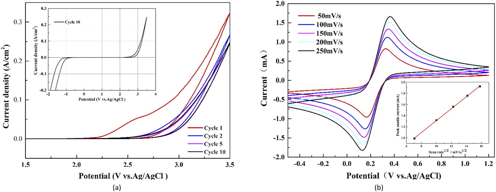 | ||
| Fig. 5 Cyclic voltammogram of the WC–Co/BDD electrode in (a) 0.5 mol L−1 H2SO4 solutions and (b) 0.1 mol L−1 KCl solution containing 0.01 mol L−1 KFe(CN)6 (scanning rate 50–250 mV s−1). | ||
Fig. 5(b) presents the cyclic voltammetric curves obtained by various scanning rates in 0.1 mol L−1 KCl solutions containing 0.01 mol L−1 KFe(CN)6. The potential is swept between −0.6 V and 1.2 V vs. Ag/AgCl. A quasi-reversible property of the redox reaction is reflected in anodic peak current (Ip,a)/cathodic peak current (Ip,c) ratio close to one and relatively low peak potential difference (ΔEp). In Fig. 5(b), all curves show the basically symmetrical redox couple peaks. In the case of 50 mV s−1, ΔEp is 161 mV; Ip,a is 0.99 mA and Ip,c is −1.01 mA, and thus Ip,a/Ip,c is 0.98. With the scan rate increasing from 50 mV s−1 to 250 mV s−1, Ip,a gradually increases from 0.99 mA to 1.93 mA, and the ΔEp value increases from 161 mV to 234 mV. Besides, the solid rectangles of Fig. 5(b) exhibit a strong linear relationship between the anodic peak current (Ip,a) and the square root of the scan rate. These characteristics of curves demonstrate a desirable quasi-reversible behaviour on the WC–Co/BDD electrode following the standard BDD.46 What's more, the reactions on the electrode surface are controlled by semi-infinite linear diffusion.45
3.3 Electrochemical stability
The service life of BDD electrodes is closely related to the pretreatment and preparation processes, as well as the service conditions.13,47 The ALT is carried out on the nanocrystalline WC–Co/BDD electrode with current density of 1 A cm−2 in 3 mol L−1 H2SO4 solutions. Satisfactorily, the cell voltage has hardly changed at about 4.5 V in 400 hours. Under the same service parameters, the life of Ti/BDD is about 370 h in ref. 28, and about 264 h in ref. 14. In contrast, the electrochemical stability of WC–Co/BDD electrode is acceptable. This may be attributed to the fact that the residual stress existing in the nanocrystalline BDD films is obviously lower than that in the microcrystalline ones,28 moreover, the low compressive stress is beneficial to the adhesion of the films. In addition, an extremely high life of more than 1500 h is represented on Ti/BDD, Si/BDD, and Nb/BDD electrodes in ref. 41, which may be ascribed to the higher coating thickness on the substrates (9–20 μm). In this work, the BDD sample with the higher thickness (7 μm) is deposited on the WC–Co substrate and its service life reaches over 1440 h by the same ALT. However, such BDD films are deposited in 10 hours and the growth rate is too slow (0.7 μm h−1).On the other hand, the dense pinholes are detected on the surfaces of the as-tested sample by FESEM at a magnification of 20![[thin space (1/6-em)]](https://www.rsc.org/images/entities/char_2009.gif) 000×, as shown in the right image of Fig. 6. This may be attributed to the fact that the nanocrystalline diamond films have a large volume fraction of the grain boundaries that contain the impurities and nondiamond sp2 carbon, which are probably removed by the electrochemical etching or generated bubbles. This phenomenon did not occur in the microcrystalline diamond films.28 Besides, the resistance of WC–Co/BDD electrode decreases after the BDD films fall off because the uncovered substrate has a lower resistivity compared with that of the boron-doped diamond. Meanwhile, the exposed WC element of the substrate is easily oxidized to form WO3 in the electrolyte solution, resulting in the serious corrosion occurred on the substrate (as presented in the left image of Fig. 6).
000×, as shown in the right image of Fig. 6. This may be attributed to the fact that the nanocrystalline diamond films have a large volume fraction of the grain boundaries that contain the impurities and nondiamond sp2 carbon, which are probably removed by the electrochemical etching or generated bubbles. This phenomenon did not occur in the microcrystalline diamond films.28 Besides, the resistance of WC–Co/BDD electrode decreases after the BDD films fall off because the uncovered substrate has a lower resistivity compared with that of the boron-doped diamond. Meanwhile, the exposed WC element of the substrate is easily oxidized to form WO3 in the electrolyte solution, resulting in the serious corrosion occurred on the substrate (as presented in the left image of Fig. 6).
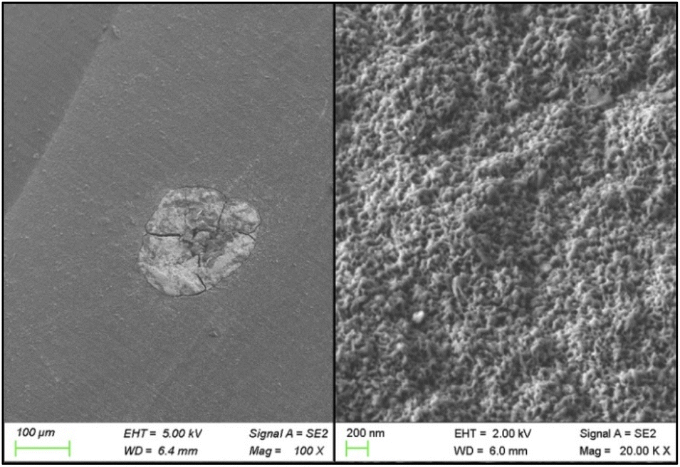 | ||
| Fig. 6 The right image of the WC–Co/BDD electrode after the ALT test by FESEM under the magnification of 20000×; left image of a corrosive hole on the WC–Co/BDD electrode after the ALT test. | ||
3.4 Activity
Fig. 7(a) shows the linear sweep voltammograms of WC–Co/BDD electrode in 0.5 mol L−1 H2SO4 solutions with different concentrations of phenol from 0 to 10 mmol L−1. In the tests, the scanning rate is 100 mV s−1 and the potential is swept from 0 to 2.8 V vs. Ag/AgCl. In order to obtain reproducible results, the electrode is pretreated by anode polarization in 0.5 mol L−1 H2SO4 at 300 mA cm−2 for 5 min before the scan. The obvious oxidation peaks around 1.5 V related to the irreversible electrochemical oxidation of phenol are observed in all curves except for the one of the blank solutions, and the potential of peaks is lower than that of water decomposition for the BDD anode. This suggests that the BDD electrodes have a higher electro-oxidation efficiency for phenol compared with the traditional metal or oxide electrode materials. Moreover, the oxidation potential of phenol (around 1.5 V) for nanocrystalline WC–Co/BDD electrode is in accordance with that for the standard microcrystalline BDD. In addition, the inset plot in Fig. 7(a) presents a relationship between the peak current and phenol concentrations. When the concentration is lower than 3 mmol L−1, the oxidation current increases with the increase of concentration, which approximately maintains a linear relationship. This implies the mass transport control in the experiment of phenol oxidation. Additionally, the current increases slowly as the concentration increases further (>3 mmol L−1), which may be caused by the formation of polymeric films on the anode surface at the high phenol concentration.9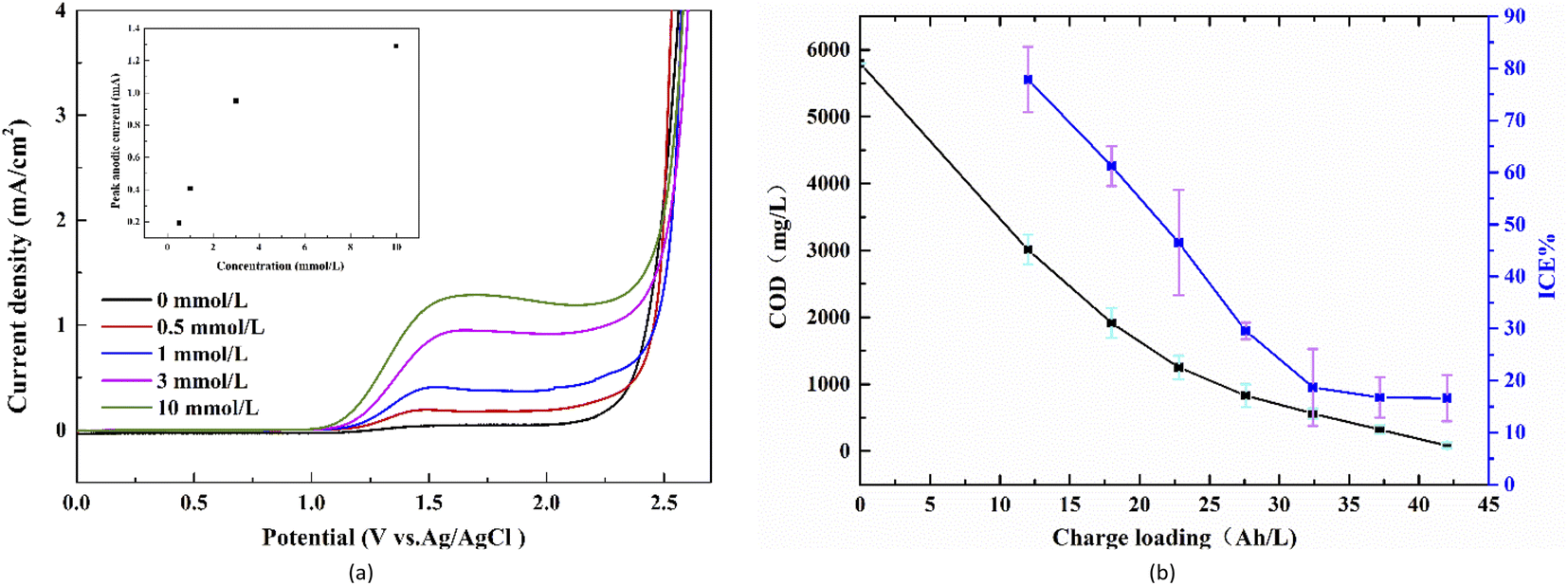 | ||
| Fig. 7 (a) Linear sweep voltammograms of the WC–Co/BDD electrode in 0.5 mol L−1 H2SO4 solutions with the different concentrations of phenol; (b) change of COD with charge loading. Current density 100 mA cm−2, H2SO4 0.5 mol L−1, temperature 25 °C. | ||
The WC–Co/BDD electrode is applied in three replicated experiments for oxidating phenol with the high concentration (25 mmol L−1) at the current density of 100 mA cm−2. Here, 0.5 mol L−1 H2SO4 is added to the simulative wastewater mainly to improve the conductivity of the solution. Fig. 7(b) presents the change curves of COD values and the instantaneous current efficiency (ICE) with the charge loading. The ICE of the electrochemical oxidation of phenol is calculated from the COD values using the following equation:
4. Conclusions
The cemented carbide (WC–Co) is applied to the substrates instead of the conventional ones such as Si, Ti, and Nb, on which the boron-doped nanocrystalline diamond (BDD) films are deposited using the hot filament chemical vapor deposition. During the films preparation, the trimethyl borate (C3H9BO3) is used as the boron source and the [B]/[C]gas is set as the atomic ratio of 5000 ppm. The physical characteristics of as-deposited WC–Co/BDD electrodes are studied by Field Emission Scanning Electron Microscopy (FE-SEM), Micro-Raman Spectroscopy, X-ray photoelectron spectroscopy (XPS), and four-point probe method. The results present that the BDD films deposited on the whole WC–Co substrate are highly uniform and pinhole-free with the grain size of 100 nm and the thickness of 4 μm. The electrochemical characteristics of WC–Co/BDD electrodes are investigated by the accelerated life test (ALT) and cyclic voltammetry. According to the results, the WC–Co/BDD electrode has a wide potential window of 3.8 V with an extremely low background current in 0.5 mol L−1 H2SO4 electrolytes and shows a desirable quasi-reversible behaviour in K3[Fe(CN)6] redox system. Satisfactorily, the electrode has a service life of over 400 h in the ALT with 3 mol L−1 H2SO4 electrolytes at a constant current density of 1 A cm−2. These electrochemical performances of BDD films on the WC–Co substrate is similar or even slightly better than that on the commonly used substrates (such as Ti, Si, and Nb). However, the electrochemical stability of WC–Co is not good, which causes the substrate to be quickly corroded after the films fall off. Finally, phenol is used as an organic pollutant to test the activity of WC–Co/BDD electrodes. The results show that the COD reduces from initial 5795 to 85 mg L−1, and the average current efficiency is about 46% (error of 2%), suggesting that the WC–Co/BDD electrode like the standard BDD exhibits a good mineralization capacity on the phenol.Conflicts of interest
There are no conflicts to declare.Acknowledgements
This research is supported by the Jiangsu Natural Science Foundation (No. BK20201142) and the National Natural Science Foundation of China (No. 51605280).Notes and references
- X. Zhu, S. Shi, J. Wei, F. Lv, H. Zhao, J. Kong, Q. He and J. Ni, Environ. Sci. Technol., 2007, 18, 6541–6546 CrossRef.
- C. Zhang, H. Lin, J. Chen and W. Zhang, Environ. Technol., 2013, 34, 2371–2376 CrossRef CAS PubMed.
- W. Hu, L. Yang, P. Shao, H. Shi, Z. Chang, D. Fang, Y. Wei, Y. Feng, Y. Huang, K. Yu and X. Luo, Environ. Sci. Technol., 2022, 56, 10412–10422 CrossRef CAS PubMed.
- H. Yuan, H. Li, L. Zhao and J. Chen, Int. J. Electrochem. Sci., 2020, 15, 2027–2038 CrossRef CAS.
- M. A. Q. Alfaro, S. Ferro, C. A. Martínez-Huitle and Y. M. Vong, J. Braz. Chem. Soc., 2006, 17, 227–236 CrossRef CAS.
- C. A. Martinez-Huitle and S. Ferro, Chem. Soc. Rev., 2006, 35, 1324–1340 RSC.
- M. Valdez-Carrillo, L. Abrell, J. Ramírez-Hernández, J. A. Reyes-López and C. Carreón-Diazconti, Environ. Sci. Pollut. Res., 2020, 27, 44863–44891 CrossRef CAS.
- H. Zanin, R. F. Teófilo, A. C. Peterlevitz, U. Oliveira, J. C. de Paiva, H. J. Ceragioli, E. L. Reis and V. Baranauskas, J. Appl. Electrochem., 2013, 43, 323–330 CrossRef CAS.
- J. Sun, H. Lu, H. Lin, L. Du, W. Huang, H. Li and T. Cui, Sep. Purif. Technol., 2012, 88, 116–120 CrossRef CAS.
- S. T. McBeath, D. P. Wilkinson and N. J. D. Graham, Environ. Sci.: Water Res. Technol., 2020, 6, 2405–2415 RSC.
- M. Santana, L. Faria and J. Boodts, Electrochim. Acta, 2005, 50, 2017–2027 CrossRef CAS.
- K. Zhang, H. Wang, Y. Zhao, Y. Xi, B. Liu, J. Xi, G. Shao, B. Fan, H. Lu, H. Xu, R. Zhang, N. Yan and Z. Wang, Appl. Surf. Sci., 2021, 568, 150977 CrossRef CAS.
- X. Chen, G. Chen, F. Gao and P. Yue, Environ. Sci. Technol., 2003, 21, 5021–5026 CrossRef PubMed.
- X. Chen, F. Gao and G. Chen, J. Appl. Electrochem., 2005, 35, 185–191 CrossRef CAS.
- S. Baluchová, A. Daňhel, H. Dejmková, V. Ostatná, M. Fojta and K. Schwarzová-Pecková, Anal. Chim. Acta, 2019, 1077, 30–66 CrossRef.
- B. P. Chaplin, I. Wyle, H. Zeng, J. A. Carlisle and J. Farrell, J. Appl. Electrochem., 2011, 41, 1329–1340 CrossRef CAS.
- R. Mei, Q. Wei, C. Zhu, W. Ye, B. Zhou, L. Ma, Z. Yu and K. Zhou, Appl. Catal., B, 2019, 245, 420–427 CrossRef CAS.
- J. L. A. de Queiroz, A. R. L. da Silva, D. C. de Moura, D. R. da Silva and C. A. Martínez-Huitle, J. Electroanal. Chem., 2017, 794, 204–211 CrossRef.
- Y. Tian, X. Chen, C. Shang and G. Chen, J. Electrochem. Soc., 2006, 153, J80–J85 CrossRef CAS.
- H. Wang, T. Webb and J. W. Bitler, Int. J. Refract. Met. Hard Mater., 2015, 49, 170–177 CrossRef CAS.
- W. Haenni, P. Rychen, M. Fryda and C. Comninellis, in Semiconductors and Semimetals, ed. C. E. Nebel and J. Ristein, Elsevier, 2004, vol. 77, pp. 149–196 Search PubMed.
- T. Zhang, Q. Feng, Z. Yu, L. Zhang and F. Sun, Int. J. Refract. Met. Hard Mater., 2019, 84, 105016 CrossRef CAS.
- T. Zhang, Y. Qian, S. Wang, G. Huang, L. Zhang and Z. Xue, Crystals, 2019, 9, 394 CrossRef CAS.
- X. Wang, J. Zhang, B. Shen, T. Zhang and F. Sun, Int. J. Refract. Met. Hard Mater., 2014, 45, 31–40 CrossRef.
- L. Wang, X. Lei, B. Shen, F. Sun and Z. Zhang, Diamond Relat. Mater., 2013, 33, 54–62 CrossRef CAS.
- K. Saito, A. Suzuki, A. Kawana and Y. Sakamoto, J. Surf. Finish. Soc. Jpn., 2017, 68, 727–732 CrossRef.
- T. Zhang, L. Wang, F. Sun, B. Shen and Z. Zhang, Diamond Relat. Mater., 2013, 40, 82–88 CrossRef CAS.
- J. J. Wei, C. M. Li, X. H. Gao, L. F. Hei and F. X. Lvun, Appl. Surf. Sci., 2012, 258, 6909–6913 CrossRef CAS.
- J. Monzon, C. Quiñones, J. Saavedra, D. Valdivia and M. Esparza, Biosci. Res., 2022, 18, 1294–1300 Search PubMed.
- X. C. Wang, C. C. Wang, W. K. He and F. H. Sun, Trans. Nonferrous Met. Soc. China, 2018, 28, 469–486 CrossRef CAS.
- S. T. Lee, Y. W. Lam, Z. Lin, Y. Chen and Q. Chen, Phys. Rev. B: Condens. Matter Mater. Phys., 1997, 55, 15937–15941 CrossRef CAS.
- T. Zhang, X. Wang, B. Shen, F. Sun and Z. Zhang, J. Cryst. Growth, 2013, 372, 49–56 CrossRef CAS.
- M. A. Fraga, A. Contin, L. A. A. Rodríguez, J. Vieira, R. A. Campos, E. J. Corat and V. J. Trava Airoldi, Mater. Res. Express, 2016, 3, 025601 CrossRef.
- A. C. Ferrari and J. Robertson, Phys. Rev. B, 2001, 63, 121405 CrossRef.
- X. Wang, X. Shen, F. Sun and B. Shen, Diamond Relat. Mater., 2017, 73, 218–231 CrossRef CAS.
- K. Schwarzová-Pecková, J. Vosáhlová, J. Barek, I. Šloufová, E. Pavlova, V. Petrák and J. Zavázalová, Electrochim. Acta, 2017, 243, 170–182 CrossRef.
- P. W. May, W. J. Ludlow, M. Hannaway, P. J. Heard, J. A. Smith and K. N. Rosser, Diamond Relat. Mater., 2008, 17, 105–117 CrossRef CAS.
- B. N. Mavrin, V. N. Denisov, D. M. Popova, E. A. Skryleva, M. S. Kuznetsov, S. A. Nosukhin, S. A. Terentiev and V. D. Blank, Phys. Lett. A, 2008, 372, 3914–3918 CrossRef CAS.
- F. M. Shakhov, A. M. Abyzov and K. Takai, J. Solid State Chem., 2017, 256, 72–92 CrossRef CAS.
- S. Ghodbane, D. Ballutaud, A. Deneuville and C. Baron, Phys. Status Solidi A, 2006, 203, 3147–3151 CrossRef CAS.
- W. Yang, J. Tan, Y. Chen, Z. Li, F. Liu, H. Long, Q. Wei, L. Liu, L. Ma, K. Zhou and Z. Yu, J. Alloys Compd., 2022, 890, 161760 CrossRef CAS.
- X. Chen, G. Chen and P. L. Yue, Chem. Eng. Sci., 2003, 58, 995–1001 CrossRef CAS.
- G. M. Swain, J. Electrochem. Soc., 1994, 141, 3382–3393 CrossRef CAS.
- S. Kim, S. H. Kim, M. Y. You, J. H. Yoon and P. K. Song, Nanosci. Nanotechnol. Lett., 2018, 10, 1–6 CrossRef.
- Z.-m. Yu, J. Wang, Q.-p. Wei, L.-c. Meng, S.-m. Hao and F. Long, Trans. Nonferrous Met. Soc. China, 2013, 23, 1334–1341 CrossRef CAS.
- L. G. Vernasqui, B. A. Kawata, A. F. Sardinha, M. A. Rodrigo and N. G. Ferreira, Diamond Relat. Mater., 2022, 121, 108793 CrossRef CAS.
- X.-R. Lu, M.-H. Ding, C. Zhang and W.-Z. Tang, Thin Solid Films, 2018, 660, 306–313 CrossRef CAS.
- C. C. C. Pulgarin, J. Appl. Electrochem., 1991, 21, 703–708 CrossRef.
- E. Weiss, K. Groenen-Serrano and A. Savall, J. Appl. Electrochem., 2008, 38, 329–337 CrossRef CAS.
| This journal is © The Royal Society of Chemistry 2022 |