DOI:
10.1039/D2RA04346G
(Paper)
RSC Adv., 2022,
12, 25163-25171
Impact of localized surface plasmon resonance on efficiency of zinc oxide nanowire-based organic–inorganic perovskite solar cells fabricated under ambient conditions†
Received
14th July 2022
, Accepted 26th August 2022
First published on 5th September 2022
Abstract
Organometal halide perovskites as hybrid light absorbers have been investigated and used in the fabrication of perovskite solar cells (PSCs) due to their low-cost, easy processability and potential for high efficiency. Further enhancing the performance of solution processed PSCs without making the device architecture more complex is essential for commercialization. In this article, the overall improvement in the performance of ZnO nanowires (NWs)-based PSCs fabricated under ambient conditions, incorporating Ag nanoparticles (NPs) delivering a device efficiency of up to 9.7% has been demonstrated. This study attributes the origin of the improved photocurrent to the improved light absorption by localized surface plasmon resonance (LSPR) with the incorporation of Ag NPs. These findings represent a basis for the application of metal NPs in photovoltaics and could lead to facile tuning of optical absorption of the perovskite layer giving higher current-density (JSC) and suppressed recombination effects leading to higher open-circuit voltage (VOC).
1. Introduction
Perovskite solar cells (PSCs) based on an organo-lead–halide light-harvesting material, the most common of which is methylammonium lead triiodide (CH3NH3PbI3),1 have been intensively investigated because of their strong absorption in a broad region of the visible spectrum, high charge-carrier mobilities,2 a large diffusion length (about 100 nm) for both electrons and holes,3,4 which lead to better device performance. By taking advantage of the outstanding characteristics of organometal halide perovskite absorbers, attractive photovoltaic performance can be obtained.5–8 Meanwhile, numerous studies suggest strong prospects for power conversion efficiency (PCE) by improving the structures and methods of preparation of PSCs.9–11 In this context, in addition to improving the quality and stability of perovskite materials, new design strategies to further enhance the PCE are essential for next-generation photovoltaics. Various efforts are currently being directed toward improving the efficiency of the perovskite-based solar cells which utilize normally mesoporous titanium dioxide (TiO2) as charge collecting layers, as well as scaffold layers, on which the CH3NH3PbI3 light absorber can be grown.12,13 However, a recent investigation showed that the low intrinsic electron mobility of TiO2 leads to an unbalanced charge transport of PSCs.14 In contrast, zinc oxide (ZnO) as a charge-collecting layer is believed to be a superior alternative to TiO2 due to the excellent bulk electron mobility than that of TiO2.15 Moreover, easy preparation of various morphologies,16 high transparency, and environmental stability of ZnO, make it particularly interesting for solar cells applications, such as organic solar cells,17 dye-sensitized solar cells (DSCs),18,19 and organic–inorganic PSCs.20–23 In the case of organic–inorganic PSCs based on ZnO nanostructures, so far, the nanoparticles (NPs) are commonly used. However, ZnO NPs are usually synthesized by relatively complex procedures, such as dilution processes, long reaction time, etc. Kim et al.,24 reported that NPs exhibit slow electron transport, which occur through particle-to-particle hopping pathway due to the presence of grain boundaries, resulting in a higher charge recombination at the ZnO/perovskite interfaces that can limit the efficiency of PSCs.25 Although faster electron transport was observed in ZnO than TiO2,26 photovoltaic performances of ZnO-based PSCs were lower than that of TiO2-based PSCs. Thus, an appropriate device structure to suppress the charge recombination is indispensable in order to improve the PCE of ZnO-based PSCs.
For further improvement of the PCE, the integration of localized surface plasmon can be an alternative because it improves the efficiency of light absorption, short-circuit current density (JSC), and hence the overall improvement of device performance. Although perovskite absorbers are already able to effectively absorb sunlight in well-operating solar cells, there are additional efficiencies that can be achieved by enhancing the absorption of light near the band edge, and the resulting thinning of solar cells. Lu et al.,27 pointed out that improved light absorption should be promising because the absorption of the PSCs falls around the edge of the band. Snaith et al.,28 also succeeded in improving the efficiency of the PSCs by using the Au@SiO2 NPs core–shell to reduce exciton binding energy, but no enhancement in light absorption was observed. To improve the light absorption of solar cells, one of the promising methods is to apply noble metal NPs, on which localized surface plasmon resonance (LSPR) can be excited under light illumination. Chen et al.,29 reported that the confined electromagnetic energy based on LSPR could greatly improve the light absorption of the active medium surrounding the NPs. Thus, the photovoltaic performance of PSCs can be improved by using metal NPs due to the improved light absorption. For a better performance without increasing the cost of fabrication, the reduction of the amount of Pb by replacing perovskite material with NPs or by employing thinner perovskite absorbers, without deteriorating the absorption is of great importance. Motivated by the desire to enhance the light absorption of the perovskite layer and to clarify its effect on the performance of the device, the study demonstrated the use of LSPR of silver (Ag) NPs in devices.
This paper presents a simple, robust fabrication method to prepare ZnO nanowires (NWs) for successful implementation as an electron transport layer (ETL) in solution-processed CH3NH3PbI3-based PSCs. Using a simple reactive evaporation technique, high aspect ratio ZnO NWs (∼52 nm average diameter, ∼455 nm length) were prepared on fluorine doped tin oxide (FTO) substrate. Law et al.,30 reported that the NWs have an internal electric field in the c-axis direction to assist charge transport, resulting in a decrease in recombination of injected electrons. Thus, it is believed that NWs would be more effective for PSCs. Thereafter, CH3NH3PbI3 perovskite films with an average thickness of about 400 nm were carefully deposited using the two-step deposition method. Then, spin-coating of poly(3-hexylthiophene-2,5-diyl) (P3HT) used here as the hole transporting layer (HTL) was carried out in ambient conditions. Prior to the growth of CH3NH3PbI3 films, the filtration of the lead iodide (PbI2) solution was carried out, and the effect of filtration on the efficiency of the devices were investigated. The result showed that proper filtration is one of the effective means of controlling the surface coverage and crystallization of the absorbers. With the aim of improving the performance of the PSCs, plasmonic NPs (Ag NPs) have been incorporated into the NWs and perovskite layer. For the growth of Ag NPs from Ag films, the PVD method was used because of the advantages of its low cost, easy process, and high controllability as well as its ability to produce uniform Ag layer on the FTO substrate. Different thicknesses of Ag films (5 nm–20 nm) were subsequently annealed to form different sizes (24 nm–95 nm average diameter) of Ag NPs. The thickness and size distributions of the Ag NPs were studied in detail and optimized to achieve the optimal level of light absorption at well-defined spectral ranges in PSCs. The investigation makes it possible to determine the redshift of the absorption spectra of Ag NPs because of the strong light–matter interaction produced by the localization of electromagnetic modes around the NPs when LSPRs are excited. The influence of Ag NPs on the optical properties of CH3NH3PbI3, and the subsequent overall performance of ZnO NWs-based PSCs fabricated in ambient conditions were systematically investigated in comparison with NPs-free PSCs. Using LSPR effects, the PCE of PSCs increased by 5.43% to 8.21% for the non-filter solution of PbI2. This number increased from 6.24% to 9.70% for the filter solution of PbI2. These results suggest that the incorporation of LSPR in the devices is an effective way to improve light absorption and charge transfer properties, which is expected to further improve the PCE of various PSCs, including Pb-free PSCs with low efficiencies. This efficiency value may not be significant possibly due to the uncontrolled fabrication environment, but rather the application of an inexpensive and easy way to improve the efficiency of the device prepared under ambient conditions was the main concentration of this study for commercialization.
2. Experimental
2.1 Materials
Highly pure metal zinc powder (99.999%, 100 mesh) and Semicoclean 23 were purchased from Furuuchi Chemical. Co. Ltd. FTO with a sheet resistivity of 7 Ω sq−1 was purchased from Solaronix S. A. For the oxidation of the Zn powder, a very pure oxygen gas (99.999%) was used. Metal silver (Ag) of high purity (99.99%) was purchased from Nilaco Corp. Methylamine (CH3NH2) solution (40% in methanol) and hydroiodic acid (HI) in water at 57% by weight were purchased from Tokyo Chemical Industries, Ltd. PbI2 of high purity (99.999%) and poly(3-hexylthiophene) (P3HT) of electronic grade (99.995% trace metals basis) were purchased from Sigma-Aldrich. N,N-Dimethylformamide (DMF), chlorobenzene, acetone, and 2-propanol were purchased from Wako Pure Chemical Industries, Ltd. For filtering the solution, a polyvinylidene difluoride (PVDF) Whatman syringe filter of around 0.20 μm pore size was purchased. The icros tape (ICROSTM Tape) was purchased from Mitsui Chemicals Inc. The ultrapure deionized water (Milli-Q Co. Ltd) used herein has a resistivity of 18.0 MΩ cm. All chemicals mentioned above were of analytical grade and were used without further purification.
2.2 Growth of ZnO nanowires
The self-organized ZnO NWs were grown on FTO glass substrate by a simple reactive evaporation method without the presence of catalysts or additives described elsewhere.31 The growth process was performed in the vacuum chamber. Prior to the growth of ZnO NWs, the FTO substrates were cleaned, and their surface treatment were performed. For cleaning, the substrates were first degreased by rubbing with a liquid detergent called Semicoclean 23, then by sonication successively with Semicoclean 23 (once), deionized water (four times), acetone (twice), and 2-propanol (twice) for 5 min per time. Subsequently, the substrates were dried with a N2 blow subjected to ultraviolet radiation in a O2 flow for 20 min for ozone treatment. The cleaned substrates were then immediately transferred to the deposition chamber and placed on top of an alumina crucible in which the high-purity zinc metal powder was loaded. Based on previous experimental results, the crucible temperature (Tcru) of the zinc, the substrate temperature (Tsub) and the growth time (tgro) were adjusted to the appropriate constant value of 400 °C, 500 °C and 30 min, respectively.31 Once the Tsub reached the target value, a continuous flow of high-purity oxygen gas was introduced into the vacuum chamber via a specially designed substrate holder consisting of nozzles to introduce oxygen very close to the substrate surface. However, the ambient pressure in the vacuum chamber (Poxy) was kept at 3.9 × 10⁻² Pa during the growth of ZnO NWs by using a controlled needle valve and pumping. The tgro was set to 30 min, then the samples were cooled to room temperature (RT) naturally under the same system pressure.
2.3 Preparation of silver nanoparticles
Firstly, the silver (Ag) films were prepared by vacuum thermal evaporation of Ag on FTO/ZnO NWs at a base pressure of 7 × 10⁻⁴ Pa with a rate of 0.05 to 0.06 nm s−1. The deposition rate of Ag films and their thickness were controlled by using an in situ with a quartz crystal sensor, thickness meter. Films mass thicknesses were maintained from 5 to 20 nm for whole experimental measurements. The properties of LSPR were regulated via annealing the Ag films. The annealing treatment of Ag films was carried out in a thermostatically controlled vacuum oven at 500 °C for 30 min in order to form different sizes (ca. 24 nm–95 nm average diameter) of Ag NPs. Subsequently, DMF was applied to cover the surface of Ag NPs using a spin coating because Ag NP is sensitive to solvents.
2.4 Synthesis of CH3NH3I and growth of CH3NH3PbI3 layer
The perovskite sensitizer methylammonium iodide (CH3NH3I) was prepared by reacting 30 mL of HI (0.227 mol) with 27.86 mL of CH3NH2 (0.273 mol) in an ice bath at 0 °C for 2 h with stirring. After stirring, the resultant solution was evaporated at 60 °C for 1 h, and the precipitate CH3NH3I was obtained. After that, CH3NH3I was washed three times with diethyl ether by stirring the solution for 30 min each time. The clean CH3NH3I, seemingly white crystal was dried overnight at 60 °C in a vacuum oven under dark conditions. Finally, dried CH3NH3I white crystal was used to prepare CH3NH3I solutions using 2-propanol at a concentration of 8 mg mL−1 for dipping PbI2-coated substrates. For the growth of the PbI2 layer on the samples, PbI2 (1.0 mol) was dissolved in anhydrous DMF at a concentration of 460 mg mL−1 followed by stirring overnight at RT. Then, filtration of PbI2 solutions was performed using 0.20 μm pore PVDF syringe filter. The PbI2 solution was then coated on the FTO/ZnO NWs layer and FTO/ZnO NWs/Ag NPs layer with a spin-coating at 2000 rpm for 15 s, then air-dried for several minutes. This procedure was repeated twice for both types of samples due to obtaining a smooth continuous film of PbI2. A similar process was conducted to deposit the PbI2 film using the non-filtrate solution of PbI2 for comparison. After drying, the PbI2-coated samples were immersed in CH3NH3I solutions discussed earlier for approximately 60 s due to the growth of the CH3NH3PbI3 perovskite layer. The colour of the samples was changed immediately from yellow to dark brown, indicating the successful formation of CH3NH3PbI3 perovskite layer. The samples were left to dry in the air at RT to allow slow evaporation of the solvent. FTO/ZnO NWs/CH3NH3PbI3 samples and FTO/ZnO NWs/Ag NPs/CH3NH3PbI3 (ca. 400 nm) samples were then heated at 100 °C on a hotplate in dark conditions for 90 min. Note that there was no significant change in the thickness of CH3NH3PbI3 layer prior to and after the addition of Ag NPs. This two-step process for the growth of CH3NH3PbI3 layers was applied because of obtaining homogeneous film coverage and crystallization as indicated in the literature.32,33
2.5 Fabrication of perovskite solar cells
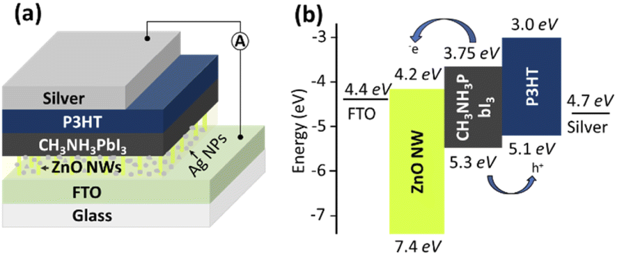
After the growth of CH3NH3PbI3 layers on FTO/ZnO NWs and FTO/ZnO NWs/Ag NPs samples, the P3HT as HTL was deposited in the air using spin-coating at 1500 rpm for 120 s. P3HT solution was prepared by mixing chlorobenzene at a concentration of 15 mg mL−1. Subsequently, an Ag electrode of about 120 nm thickness was deposited on the P3HT layer by vacuum thermal evaporation at a base pressure of 7 × 10⁻⁴ Pa with a rate of 0.1 nm s−1 to complete the devices. Finally, four types of devices and five of each group (i.e., 20 devices) using Ag NPs and without using Ag NPs with a filter and non-filter solution of PbI2 were prepared for comparison. The structures of the device that use Ag NPs, and the energy level diagram are illustrated in Fig. 1. The active area of the cell was maintained at 0.79 cm2, and the rest of the area was masked with an icros tape due to the protection against unnecessary illumination during measurement and fabrication. Most of the fabrication stages of the devices were performed under ambient conditions, except for evaporation of the top contact Ag.
 |
| | Fig. 1 Schematic illustration of the PSCs structures (a) with Ag NPs, and (b) energy level diagram. | |
2.6 Physical properties characterization of the samples
The surface morphology and microstructural characterization of the samples were performed using a field-emission scanning electron microscopy (FE-SEM; JEOL, JSM-6340F) and a high-resolution transmission electron microscope (TEM; Hitachi H-7650). The coverage of the samples obtained from FE-SEM images was evaluated using ImageJ 1.45 software.34 The structural and phase characterization was carried out using X-ray diffraction (XRD). The XRD patterns were recorded using Bruker AXS (D8 ADVANCE) X-ray diffractometer equipped with a Cu Kα (λ = 1.54056 Å) X-ray tube operated at 40 kV and 40 mA using a step size of 0.02° and a time per step of 2 s. Under these conditions, the experimental setup of the XRD measurement was performed from 20° to 70° in the 2θ ranges.
2.7 Optical properties characterization of the samples
The UV-Vis absorption spectra of the samples were acquired using a Shimadzu UV-vis-NIR scanning spectrophotometer (UV-3100 PC) coupled with an integrating sphere. The measurement was performed at RT with an incident beam angle of 0°. The luminescence spectra were measured by photoluminescence (PL: Spectrofluorometer; JASCO, FP-8300) measurement under RT with an excitation wavelength of 325 nm.
2.8 Electrical properties characterization
The current density–voltage (J–V) characteristics of the devices were measured using Keithley 2100 unit in the dark and under an illumination of the 100 mW cm−2 AM1.5G spectrum using a xenon-lamp-based solar simulator (Oriel LCS-100). The measurements were carried out using metallic shadow masks to define the active area of the device and avoid any edge effects for small area solar cell.
3. Results and discussion
3.1 Morphological, compositional, and structural properties of the samples
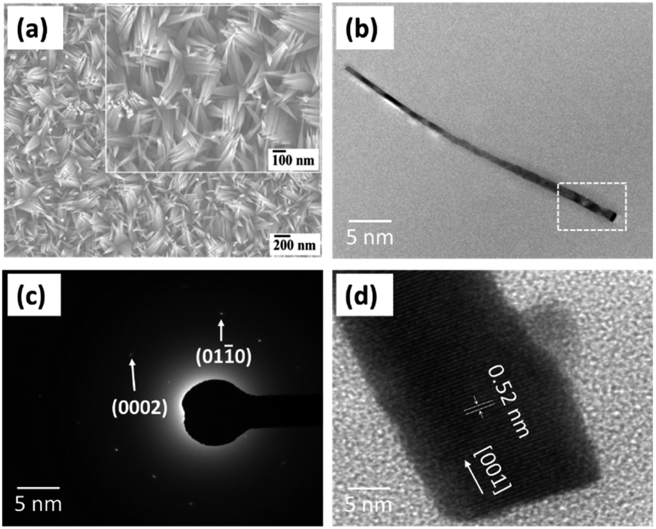
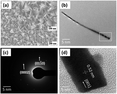
The optimal growth conditions for ZnO NWs were described elsewhere,31 and were selected at a Tsub of 500 °C with a constant Tcru of 400 °C and a Poxy of 3.9 × 10⁻² Pa. Fig. 2(a) shows the FE-SEM image of ZnO NWs grown on FTO glass substrate at a Tsub of 500 °C for 30 min. The average diameter and length of the ZnO NWs are about 52 nm and 455 nm, respectively. It is noticeable that very dense ZnO NWs have needle-like tapered ends. For a detailed study of the structure and crystalline nature of the synthesized NWs, TEM observation was conducted. Fig. 2(b)–(d) show the typical TEM image, selected area electron diffraction (SAED) pattern, and high-resolution TEM (HRTEM) image of the ZnO NW grown at 500 °C for 30 min, respectively. To prepare the sample for TEM measurements, the NWs array was separated from the substrate via sonication. As shown in Fig. 2(b), the NW is clean due to its smooth surface which extends over its whole length. It is also clear that the NW is gradually narrowing towards the tip. Almost no dislocation or stacking defects were found, indicating the high-crystalline quality of ZnO NWs. The SAED pattern obtained from the NWs shown in Fig. 2(c), where the shiny circular spots also confirm their single crystalline nature. The HRTEM image displayed in Fig. 2(d) obtained from the encircled region in Fig. 2(b). The lattice spacing along the growth direction is approximately 0.52 nm, corresponding to the (002) crystal plane of hexagonal wurtzite ZnO. This result suggests that the NWs grow preferentially along the c-axis. For the elemental analysis of the NWs, EDX measurements were performed. The results confirm that the ZnO NWs consist of Zn and O elements without other metal elements. The estimated molar ratio of Zn and O in ZnO NW is ca. 1![[thin space (1/6-em)]](https://www.rsc.org/images/entities/char_2009.gif) :1. This is reasonably consistent with the results of the XRD pattern analysis that will be discussed later.
:1. This is reasonably consistent with the results of the XRD pattern analysis that will be discussed later.
 |
| | Fig. 2 (a) FE-SEM image, (b) typical TEM image, (c) selected area electron diffraction (SAED) pattern, and (d) high-resolution TEM (HRTEM) image obtained from ZnO NWs grown at 500 °C for 30 min. | |
In order to investigate the LSPR effects on the performance of PSCs, various sizes of plasmonic NPs (Ag NPs) were prepared and eventually incorporated into the NWs and perovskite thin layers. A very simple, low cost, and controllable PVD method was used to deposit Ag films, and then annealed to form Ag NPs. Ag film thicknesses were maintained from 5 to 20 nm for all experimental measurements. The annealing of the Ag films was conducted in a thermostatically controlled vacuum oven at 500 °C for 30 min, as the same temperature is necessary for the growth of ZnO NWs discussed earlier in Sections 2.2 and 2.3. Under this temperature, surface tension occurs the integration of metal atoms to form particles. SEM images of different sizes of Ag NPs (ca. 24 nm–95 nm average diameter) grown on FTO substrates are shown in ESI Fig. S1.† The formation and distribution of NPs become more uniform after the annealing treatment of Ag films with a thickness of 5–12 nm, as shown in Fig. S1.† However, as the film thickness increases by more than 12 nm, NPs tend to lose their spherical form, which seems elongated and island. It should be noted that both small and large NPs are observed for a specific film thickness, but the average size of NP increases with increasing film thickness. Therefore, film thickness has a significant impact on NP size in this study since annealing time and temperature are constant. Particle size distributions were estimated from SEM images using the manual method with ImajeJ1.45 software. The estimated average diameters of the Ag NPs are approximately 24 nm, 38 nm, 52 nm, 61 nm, 72 nm and 95 nm for the film thicknesses of 5 nm, 8 nm, 10 nm, 12 nm, 15 nm and 20 nm, respectively. It is worth mentioning that the size and distribution of Ag NPs are very critical for achieving the high PCE of PSCs. For Ag NPs with a size much smaller than the wavelength of the excited light (R ≪ λext), the electrostatic polarizability (α) of NP can be described using the following eqn (1):35
| | |
α = 4πa2(ε − εm)/(ε + 2εm)
| (1) |
where
α is the electrostatic polarizability of NPs,
ε is the optical dielectric constant of metal,
εm is the optical dielectric constant of the medium;
a is the radius of a spherical NP. Eqn
(1) reveals that the permittivity of the surrounding environment (
εm) significantly affects the value of
α for the NP. Parameter,
α determines the absorption, scattering and extinction spectra of Ag NPs.
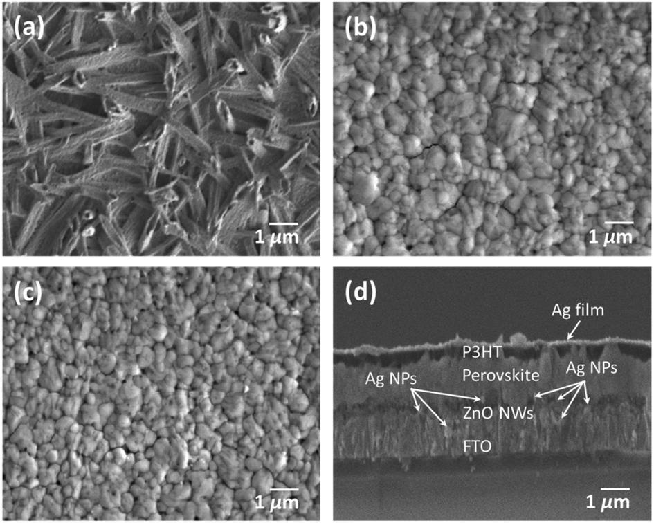
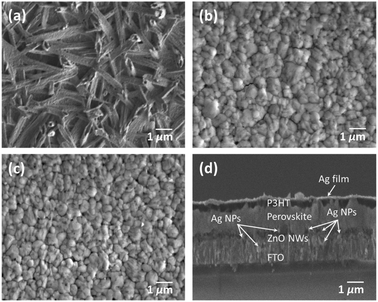
Furthermore, to investigate the morphology of the CH3NH3PbI3 perovskite film grown on FTO/ZnO NWs and FTO/ZnO NWs/Ag NPs using the two-step deposition method in the ambient condition, FE-SEM measurements were conducted. Fig. 3(a) and (b) show the FE-SEM images of CH3NH3PbI3 films prepared without filter and with filter solution of PbI2, respectively. As can be seen in Fig. 3(a), non-uniform domains in CH3NH3PbI3 crystals are formed. This may be due to a partial conversion of PbI2 and CH3NH3I. As a result, a high proportion of PbI2(s) did not react completely with CH3NH3I(aq) to form the CH3NH3PbI3(s) phase (PbI2 + CH3NH3I ↔ CH3NH3PbI3). However, a perovskite layer with relatively uniform cubic crystals is formed for the case of filter solution of PbI2, as shown in Fig. 3(b). Fig. 3(c) also shows the FE-SEM image of CH3NH3PbI3 films prepared with filter solution of PbI2 with Ag NPs (ca. 61 nm). Here also, fairly uniform cubic crystals are formed. Average roughness values for perovskite films without Ag NPs and with Ag NPs are estimated to be approximately 10.2 and 12.5 nm, respectively. No significant changes in surface morphology of perovskite are observed between the cases without Ag NPs and with addition of Ag NPs. Fig. 3(d) shows the cross-section image of PSC. The thickness of the film is estimated to be around 400 nm, and the average size of the crystal is large, approximately 310 nm. It is reported that crystals with large grain sizes are favorable for charge transport, and it acts as a scattering centre of incident light, therefore preferable to obtain high performance devices.36 It can be attributed that the filter solution of PbI2 can change the morphology and structure of CH3NH3PbI3 film that may have an enormous impact on the performance of PSCs.
 |
| | Fig. 3 FE-SEM image of perovskite film obtained (a) without a filter solution of PbI2, (b) with a filter solution of PbI2, (c) with a filter solution of PbI2 with Ag NPs, and (d) cross-section image of PSC (FTO/ZnO NWs/Ag NPs/CH3NH3PbI3/P3HT/Ag). | |
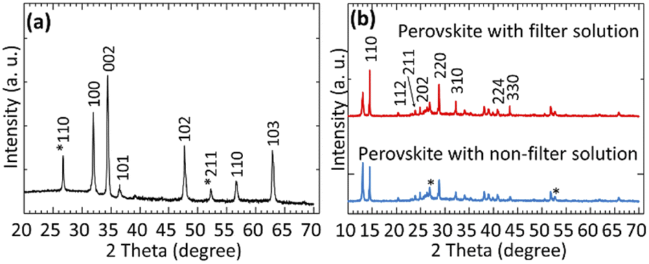
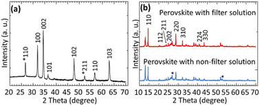
The XRD measurement was carried out to investigate the different physical properties such as structure and crystal phase of the prepared NWs. Fig. 4(a) shows the XRD patterns of ZnO NWs grown on FTO substrate at 500 °C for 30 min. The peaks that appeared at 2θ = 31.91°, 34.43°, 36.57°, 47.66°, 57.26° and 63.17° represent the (100), (002), (101), (102), (110) and (103) phases, respectively, of the hexagonal close-packed crystal structure of the ZnO according to the Joint Committee on Powder Diffraction Standards (JCPDS) card no. 00-001-1136. Crystal planes (100), (002) and (101) are noted to belong to the hexagonal wurtzite structure, with no excess peaks of impurities (i.e., metal Zn, etc.) detected in the XRD spectrum, thereby confirming the complete conversion of metal Zn powder to ZnO. Among all peaks, the relatively higher peak intensity obtained on the plane (002) indicates that the prepared NPs are oriented preferably along the c-axis, and the relative sharpness of the peak indicates the large crystal size.37 On the other hand, the peaks that appeared at 2θ = 26.73° and 52.25° can be attributed to the FTO, which belongs to phases (110) and (211), respectively. These results are consistent with the standard JCP data number (01-072-1147). The average size (diameter) of the NW was estimated by the Debye–Scherrer's equation using the full width at half maximum (FWHM) value of the XRD diffraction peaks corresponding to the planes (110) and (002). The Debye–Scherrer's equation can be written as follows (2):38
| | |
D = kλ/βcosθ
| (2) |
where
D is the crystal size in Å,
k is a Scherrer coefficient (0.9),
λ is the wavelength of X-ray (0.15418 nm),
β is the FWHM of the diffraction peak in radian, and
θ is the diffraction peak angle. The average crystal diameter of NWs determined using (002) diffraction peak is approximately 49.0 nm. The NW size derived from the XRD measurements is reasonably consistent with the values determined by the SEM image analysis.
Fig. 4(b) shows the XRD patterns of CH
3NH
3PbI
3 perovskite films grown on FTO substrate using non-filter solution of PbI
2 and filter solution of PbI
2 by the two-step deposition method under ambient condition. The strong diffraction peaks that appeared at 2
θ = 14.08°, 28.41°, 31.85°, and 43.19° represent the (110), (220), (310), and (330) planes, respectively, of the cubic CH
3NH
3PbI
3. These results are consistent with the previous research reported in ref.
33,
39 and
40 indicating the formation of a highly crystalline perovskite structure. However, there are a few peaks not mentioned above that indicate the presence of untreated or partially reacted PbI
2 that may affect the morphology and optical properties of perovskite film.
 |
| | Fig. 4 XRD pattern of (a) ZnO NWs, and (b) perovskite film deposited using non-filter solution of PbI2 and filter solution of PbI2. | |
3.2 Optical properties of the samples
The optical properties of metal NPs greatly depend on their sizes, shapes, chemical compositions, and the surrounding dielectric environment. In order to investigate the size dependent LSPR of Ag NPs, optical measurements were conducted. The total reflectance (R) and total transmittance (T) of the reference and Ag NPs loaded films were collected using UV-vis-NIR scanning spectrophotometer coupled with an integrating sphere. Using T and R, optical absorption (A) was estimated as A = 1 − R − T. Absorption spectra obtained from different sizes of Ag NPs (ca. 24–95 nm) grown on FTO substrate is shown in ESI Fig. S2.† The maximum intensities of the peaks are increased by increasing the thickness of the Ag films. As the average size of the NPs increased by increasing the thickness of the Ag films obtained from the SEM image analysis, the absorptions progressively increased and shifted to the red by increasing the size of Ag NPs, as shown in ESI Fig. S2.† The peaks shifted to the red could be attributed to the LSPR induced by Ag NPs.41 It should be noted that the LSPR results in strong local EM fields, and there are improvements not only in EM fields but also in the efficiency of scattering when the size of Ag NPs increases. Higher scattering tends to reduce absorption, and hence larger NPs tend to absorb less at shorter wavelengths, while peaks in the absorption spectra have shown a progressively red shifted and broadening in the visible wavelength because of LSPR. Furthermore, two distinct resonance peaks were clearly observed at wavelengths ∼350 to 360 nm and ∼480 to 540 nm in the measured spectra that emerged from the plasmon modes associated with quadrupole and dipole in Ag NPs, respectively. In the case of a 5 nm film thickness (24 nm average diameter of the Ag NPs), quadrupole resonance peak was not observed but the peak of dipole resonance began to decrease for a film thickness of 20 nm (95 nm average diameter of the Ag NPs) due to high scattering effects. The strongest dipole resonance peak observed from different NP sizes (avg. diameter) at different wavelengths is presented in detail in ESI Table S1.† Among these, the strongest response of LSPR is observed for a film thickness of 12 nm (61 nm average diameter of the Ag NPs) without taking into account the high scattering effects. Besides, the DMF solvent effect on the optical properties of Ag NPs was not observed.
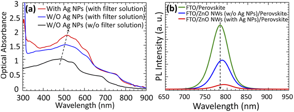
To confirm the effects of LSPR in CH3NH3PbI3, this study carried out a control experiment by incorporating Ag NPs into the CH3NH3PbI3 layer. Ag NPs with a diameter of approximately 61 nm was used because of the high LSPR responses observed in this study. Fig. 5(a) shows the UV-vis absorption spectra of CH3NH3PbI3 perovskite films grown on FTO/ZnO NWs and FTO/ZnO NWs/Ag NPs samples using filter and non-filter solutions of PbI2. Absorption of FTO/ZnO NWs was subtracted for all samples, and the absorption was adjusted to 300 to 900 nm. The absorption spectra obtained from CH3NH3PbI3 cover almost the visible to near infrared wavelength range of approximately 320–800 nm. This corresponds to an energy bandgap of ca. 1.5 eV for CH3NH3PbI3 perovskite. By incorporating Ag NPs between ZnO NWs and CH3NH3PbI3, a significant increase in optical absorption was observed for filter solution of PbI2 case, as can be seen in Fig. 5(a). The position of the absorption peak is shifted from ca. 490 nm to a longer wavelength of 518 nm due to the light trapping of LSPR arises mainly from Ag NPs. The increase in absorption could be attributed to the improvement of the electric field around the NPs as well as the increase in light scattering, which increased the length of the optical path, as discussed previously published report.42 Therefore, these findings assure the plasmon effect of Ag NPs and the filtration effect of PbI2 solution, and their effectiveness in increasing the collection of light which leads to higher efficiency of charge generation in the PSCs. To understand the charge transfer functions of Ag NPs, this study measured the charge generation/separation properties in perovskite by PL characterization. Fig. 5(b) shows the PL spectra obtained from FTO/CH3NH3PbI3, FTO/ZnO NWs (w/o Ag NPs)/CH3NH3PbI3, and FTO/ZnO NWs (with Ag NPs)/CH3NH3PbI3 samples grown with PbI2 filter solution. A significant quenching effect can be observed when the ZnO NWs forms a contact with CH3NH3PbI3. Almost completely PL quenching is displayed when the Ag NPs is integrated into the ZnO NWs. This strong PL quenching may be caused by the LSPR of Ag NPs induces a more rapid charge transfer at the interface, resulting in the suppression of charge recombination. This means that the open-circuit voltage (VOC) should be increased, as discussed in the following section.
 |
| | Fig. 5 (a) UV-vis absorption spectra of CH3NH3PbI3 film grown on FTO/ZnO NWs, and FTO/ZnO NWs/Ag NPs using filter and non-filter solutions of PbI2. (b) PL spectra of FTO/CH3NH3PbI3, FTO/ZnO NWs (w/o Ag NPs)/CH3NH3PbI3, and FTO/ZnO NWs (with Ag NPs)/CH3NH3PbI3 film grown with PbI2 filter solution. | |
3.3 Photovoltaic performance measurement
The photovoltaic performances of the devices with Ag NPs and without Ag NPs using a filter and non-filter solution of PbI2 were characterized by J–V measurements under simulated AM1.5G solar irradiation at 100 mW cm−2 in the air, as shown in Fig. 6. It is clearly demonstrated that both VOC and JSC are increased after the use of a PbI2 filter-solution in devices. The PbI2 filter-solution increased the crystallinity, grain size, surface coverage and morphology of CH3NH3PbI3 perovskite film, which may lead to higher performance of the PSCs. Excellent device initially optimized by using filter solution of PbI2 without Ag NPs shows a JSC of 11.5 mA cm−2, a VOC of 0.93 V, and a fill factor (FF) of 0.58 leading to a PCE of 6.24%. On the other hand, the device prepared with a non-filter solution of PbI2 without Ag NPs shows that the JSC, VOC, FF, and PCE values are about 10.1 mA cm−2, 0.90 V, 0.59, and 5.43%, respectively. Consequently, filtration of the PbI2 solution has a significant contribution to the improvement of the PCE of the PSCs. To further improve the performance of devices, the effect of Ag NPs on the PCE of PSCs was investigated. J–V measurements were further performed for devices prepared with Ag NPs using a filter and non-filter solution of PbI2. As can be seen in Fig. 6, the VOC and JSC are increased after the use of PbI2 filter-solution with Ag NPs in the devices. The device prepared with PbI2 filter solution using Ag NPs has a peak PCE of 9.7%, whereas the device prepared without PbI2 filter solution using Ag NPs exhibited a PCE of 8.21%. Compared to devices with and without Ag NPs that used the PbI2 filter solution, the VOC and FF were increased in general (VOC: from 0.93 to 1.03 V; FF: from 0.58 to 0.65), whereas the JSC increased significantly from 11.5 to 14.4 mA cm−2 because of the LSPR effect on devices.
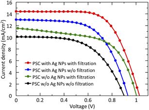 |
| | Fig. 6 J–V curves of the best performance devices prepared with a filter and non-filter solution of PbI2, without the use of Ag NPs and with the use of Ag NPs. | |
From Fig. 6, it can be clearly observed that the JSC of PSCs using a filter solution of PbI2 with Ag NPs are considerably higher than those without Ag NPs. The higher JSC may be attributed to enhanced optical absorption by LSPR from Ag NPs. Note that the LSPR leads to enhanced local electric fields and optical extinction that depend on the size of NPs. Zhang et al.28 reported that the origin of the improved JSC would be the improved generation of free carriers with the incorporation of metal NPs in the PSCs. Therefore, it can be concluded that the incorporation of Ag NPs improved the performance of the device by increasing optical absorption, and subsequent JSC as well as VOC. The enhancement of VOC can be due to the suppression of charge recombination in the presence of NPs. For an ideal p–n junction, VOC can be given by VOC = (kT/q)ln(Iph/IS) + 1, where k is the Boltzmann constant, T is the temperature, q is the electronic charge, Iph is the photocurrent, and IS the diode saturation current. The VOC depend on Iph and IS, while the IS subject to recombination. Thus, VOC then measure the amount of recombination. Lu et al.27 also reported that the increase in VOC is expected to be due to the suppression of recombination charge. Thus, the presence of Ag NPs in PSCs may be attributed to the faster transfer of charge. The corresponding results based on the J–V measurements are summarized in detail in Table 1.
Table 1 Photovoltaic performance parameters of the ZnO NWs based-PSCs without Ag NPs and with Ag NPs using non-filter and filter solution of PbI2 derived from J–V measurements
| Solar cell |
PbI2 solution type |
VOC (V) |
JSC (mA cm−2) |
FF |
PCE (%) |
| PSCs without Ag NPs |
Non-filter |
Avg. |
0.85 ± 0.05 |
8.5 ± 1.6 |
0.55 ± 0.04 |
4.37 ± 1.06 |
| Best |
0.90 |
10.1 |
0.59 |
5.43 |
| Filter |
Avg. |
0.90 ± 0.03 |
10.0 ± 1.5 |
0.55 ± 0.03 |
5.21 ± 1.03 |
| Best |
0.93 |
11.5 |
0.58 |
6.24 |
| PSCs with Ag NPs |
Non-filter |
Avg. |
0.95 ± 0.06 |
11.8 ± 1.2 |
0.61 ± 0.02 |
7.23 ± 0.98 |
| Best |
1.01 |
13.0 |
0.63 |
8.21 |
| Filter |
Avg. |
0.98 ± 0.05 |
13.5 ± 0.92 |
0.63 ± 0.02 |
9.02 ± 0.68 |
| Best |
1.03 |
14.4 |
0.65 |
9.70 |
4. Conclusions
The studies discussed in this paper were intended to understand the effects of LSPR on the efficiency of ZnO NWs-based PSCs fabricated under ambient conditions. In order to achieve these objectives and appropriately develop the enhanced PSCs, the study focused mainly on three different strategies: the use of high crystalline ZnO NWs due to high efficiency in charge collection; filtration of PbI2 solution to obtain uniform surface coverage of perovskite films; and the application of plasmonic Ag NPs to improve the optical absorption resulting in a higher performance of the devices. From this point of view, ZnO NWs were grown on FTO substrate without the presence of any catalysts through the RE method, which is very simple, controllable, and inexpensive. The optimized growth of ZnO NWs was obtained at a Tsub of 500 °C with a tgro of 30 min while maintaining the Tcru at 400 °C and Poxy to 3.9 × 10⁻² Pa. The diameter and length of the resulting NWs are approximately 52 nm and 455 nm, respectively. ZnO NWs possess network-like morphology with highly crystalline nature, which would be favorable to the efficient transport of charge in the PSCs. Subsequently, plasmonic NPs (Ag NPs) were incorporated into ZnO NWs due to the increased PCE of the device. For the fabrication of Ag NPs (24 nm–95 nm average diameter), Ag films of various thicknesses (5 nm–20 nm) were deposited using the PVD method followed by thermal annealing. The size, shape and density of the Ag NPs were controlled by setting different thicknesses of Ag films. From the FE-SEM and UV-vis absorption spectroscopy measurements, the most uniform size, distribution and LSPR responses were observed for a NP size of 61 nm (12 nm film thickness). Thus, Ag NPs with an average diameter of 61 nm were used and incorporated into NWs and thin layer of perovskite. The formation of CH3NH3I, CH3NH3PbI3 and P3HT layers were carried out under ambient condition due to the simplicity and inexpensive processing technique. In the growth of CH3NH3PbI3, the effects of filtration of the PbI2 solution were considered. For a PbI2 filter solution, the surface of the CH3NH3PbI3 film was relatively homogeneous, uniform with high surface coverage, while it was not uniform and fibre-like structure with voids in the case of PbI2 non-filter solution. In addition, conversion of PbI2 to CH3NH3PbI3 was partial because of unreacted PbI2 which was relatively higher for the non-filter solution confirmed by the XRD measurements. Therefore, filtration of PbI2 solution during the formation of CH3NH3PbI3 film is crucial. To sum up, a two-step deposition method was used for the fabrication of ZnO NWs based PSCs. For the best performance device using filter solution of PbI2 without Ag NPs, the PCE obtained is 6.24%, while it is 5.43% for non-filter case. Despite the significant effect of filtration of PbI2-solution, the obtained PCE of solar cell remains low compared to presently reported value. By incorporating Ag NPs into the devices, the PSCs showed an improved PCE of 9.70% in the case of PbI2 filter solution, but it is 8.21% in the case of non-filter solution. This improvement in efficiency may be explained by an improvement in light absorption of perovskite due to the LSPR of Ag NPs, which leads to an improvement in electron collection and device performance. We note, however, that further research is necessary to fully optimize the various layers of the device and the shape of the NPs that would improve the performance of PSCs.
Author contributions
Md. Mijanur Rahman – conceptualization, methodology, validation, investigation, visualization, data curation, writing original draft, manuscript revision and funding acquisition; Tabassum Hasnat Reshmi – investigation, data discussion, manuscript writing and revision; Suhel Ahmed – investigation, data discussion and manuscript revision; Md. Ashraful Alam – conceptualization, methodology, investigation, discussion and suggestions, manuscript writing and revision.
Conflicts of interest
The authors declare that they have no conflict of interest.
Acknowledgements
This work was partly supported by Chiba University's Global COE program Advanced School for Organic Electronics from the Ministry of Education, Culture, Sports, Science and Technology, Japan.
Notes and references
- G. Hodes, Science, 2013, 342, 317–318 CrossRef CAS PubMed.
- C. C. Stoumpos, C. D. Malliakas and M. G. Kanatzidis, Inorg. Chem., 2013, 52, 9019–9038 CrossRef CAS PubMed.
- G. Xing, N. Mathews, S. Sun, S. S. Lim, Y. M. Lam, M. Grätzel, S. Mhaisalkar and T. C. Sum, Science, 2013, 342, 344–347 CrossRef CAS PubMed.
- S. D. Stranks, G. E. Eperon, G. Grancini, C. Menelaou, M. J. P. Alcocer, T. Leijtens, L. M. Herz, A. Petrozza and H. J. Snaith, Science, 2013, 342, 341–344 CrossRef CAS PubMed.
- W. S. Yang, J. H. Noh, N. J. Jeon, Y. C. Kim, S. Ryu, J. Seo and S. I. Seok, Science, 2015, 348, 1234–1237 CrossRef CAS PubMed.
- W. Nie, H. Tsai, R. Asadpour, J.-C. Blancon, A. J. Neuki, G. Gupta, J. J. Crochet, M. Chhowalla, S. Tretiak, M. A. Alam, H.-L. Wang and A. D. Mohite, Science, 2015, 347, 522–525 CrossRef CAS PubMed.
- H. Zhou, Q. Chen, G. Li, S. Luo, T. bSong, H.-S. Duan, Z. Hong, J. You, Y. Liu and Y. Yang, Science, 2014, 345, 542–546 CrossRef CAS PubMed.
- N. J. Jeon, J. H. Noh, W. S. Yang, Y. C. Kim, S. Ryu, J. Seo and S. I. Seok, Nature, 2015, 517, 476–480 CrossRef CAS PubMed.
- N. G. Park, J. Phys. Chem. Lett., 2013, 4, 2423–2429 CrossRef CAS.
- M. Liu, M. B. Johnston and H. J. Snaith, Nature, 2013, 501, 395–398 CrossRef CAS.
- H. J. Snaith, J. Phys. Chem. Lett., 2013, 4, 3623–3630 CrossRef CAS.
- T. Homola, J. Pospisil, M. Shekargoftar, T. Svoboda, M. Hvojnik, P. Gemeiner, M. Weiter and P. Dzik, ACS Appl. Energy Mater., 2020, 3(12), 12009–12018 CrossRef CAS.
- R. D. Chavan, P. Yadav, A. Nimbalkar, S. P. Bhoite, P. N. Bhosale and C. K. Hong, Sol. Energy, 2019, 186, 156–165 CrossRef CAS.
- C. S. Ponseca Jr, T. J. Savenije, M. Abdellah, K. Zheng, A. Yartsev, T. Pascher, T. Harlang, P. Chabera, T. Pullerits, A. Stepanov, J. P. Wolf and V. Sundström, J. Am. Chem. Soc., 2014, 136, 5189–5192 CrossRef.
- D. C. Look, D. C. Reynolds, J. R. Sizelove, R. L. Jones, C. W. Litton, G. Cantwe and W. C. Harsch, Solid State Commun., 1998, 105, 399–401 CrossRef CAS.
- K. Mahmood, S. B. Park and H. J. Sung, J. Mater. Chem. C, 2013, 1, 3138–3149 RSC.
- A. Puetz, T. Stubhan, M. Reinhard, O. Loesch, E. Hammarberg, S. Wolf, C. Feldmann, H. Kalt, A. Colsmann and U. Lemmer, Sol. Energy Mater. Sol. Cells, 2011, 95, 579–585 CrossRef CAS.
- L. Li, T. Zhai, Y. Bando and D. Golberg, Nano Energy, 2012, 1, 91–106 CrossRef CAS.
- A. I. Hochbaum and P. Yang, Chem. Rev., 2010, 110, 527–546 CrossRef CAS PubMed.
- K. Mahmood, B. S. Swain and A. Amassian, Nanoscale, 2014, 6, 14674–14678 RSC.
- J. Kim, G. Kim, T. K. Kim, S. Kwon, H. Back, J. Lee, S. H. Lee, H. Kang and K. Lee, J. Mater. Chem. A, 2014, 2, 17291–17296 RSC.
- F. J. Ramos, M. C. Lopez-Santos, E. Guillen, M. K. Nazeeruddin, M. Grätzel, A. R. Gonzalez-Elipe and S. Ahmad, ChemPhysChem, 2014, 15, 1148–1153 CrossRef CAS PubMed.
- J. Dong, Y. Zhao, J. Shi, H. Wei, J. Xiao, X. Xu, J. Luo, J. Xu, D. Li, Y. Luo and Q. Meng, Chem. Commun., 2014, 50, 13381–13384 RSC.
- H. S. Kim, S. H. Im and N. G. Park, J. Phys. Chem. C, 2014, 118, 5615–5625 CrossRef CAS.
- H. S. Kim, J. W. Lee, N. Yantara, P. P. Boix, S. A. Kulkarni, S. Mhaisalkar, M. Grätzel and N. G. Park, Nano Lett., 2013, 13, 2412–2417 CrossRef CAS PubMed.
- D.-Y. Son, J.-H. Im, H.-S. Kim and N.-G. Park, J. Phys. Chem. C, 2014, 118, 16567–16573 CrossRef CAS.
- Z. Lu, X. Pan, Y. Ma, Y. Li, L. Zheng, D. Zhang, Q. Xu, Z. Chen, S. Wang, B. Qu, F. Liu, Y. Huang, L. Xiao and Q. Gong, RSC Adv., 2015, 5, 11175–11179 RSC.
- W. Zhang, M. Saliba, S. D. Stranks, Y. Sun, X. Shi, U. Wiesner and H. J. Snaith, Nano Lett., 2013, 13, 4505–4510 CrossRef CAS PubMed.
- H. Chen, L. Shao, Q. Li and J. Wang, Chem. Soc. Rev., 2013, 42, 2679–2724 RSC.
- M. Law, L. E. Greene, J. C. Johnson, R. Saykally and P. Yang, Nat. Mater., 2005, 4, 455–459 CrossRef CAS PubMed.
- M. M. Rahman and T. H. Reshmi, Curr. Appl. Phys., 2022, 41, 32–40 CrossRef.
- J. H. Im, C. R. Lee, J. W. Lee, S. W. Park and N. G. Park, Nanoscale, 2011, 3, 4088–4093 RSC.
- J. Burschka, N. Pellet, S. J. Moon, R. H. Baker, P. Gao, M. K. Nazeeruddin and M. Grätzel, Nature, 2013, 499, 316–319 CrossRef CAS PubMed.
- G. P. Ribeiro, R. S. Valotto, J. P. de Oliveira, M. C. C. Guimarães and D. Lenz, Chem. Pap., 2020, 74, 2821–2824 CrossRef CAS.
- N. G. Khlebtsov, Quantum Electron., 2008, 38, 504–529 CrossRef CAS.
- Z. Liang, S. Zhang, X. Xu, N. Wang, J. Wang, X. Wang, Z. Bi, G. Xu, N. Yuan and J. Ding, RSC Adv., 2015, 5, 60562–60569 RSC.
- W. J. Li, E. W. Shi, W. Z. Zhong and Z. W. Yin, J. Cryst. Growth, 1999, 203, 186–196 CrossRef CAS.
- B. D. Cullity, Elements of X-ray Diffractions, Addison-Wesley, USA, 2nd edn, 1978, p. 102 Search PubMed.
- Q. Chen, H. Zhou, Z. Hong, S. Luo, H. S. Duan, H. H. Wang, Y. Liu, G. Li and Y. Yang, J. Am. Chem. Soc., 2014, 136, 622–625 CrossRef CAS PubMed.
- D. Liu and T. L. Kelly, Nat. Photonics, 2013, 8, 133–138 CrossRef.
- K.-C. Lee, S.-J. Lin, C.-H. Lin, C.-S. Tsai and Y.-J. Lu, Surf. Coat. Technol., 2008, 202, 5339–5342 CrossRef CAS.
- K. Chan, M. Wright, N. Elumalai, A. Uddin and S. Pillai, Adv. Opt. Mater., 2017, 5, 1600698 CrossRef.
|
| This journal is © The Royal Society of Chemistry 2022 |
Click here to see how this site uses Cookies. View our privacy policy here. 
 Open Access Article
 This Open Access Article is licensed under a Creative Commons Attribution-Non Commercial 3.0 Unported Licence
 *ab,
Tabassum Hasnat Reshmic,
Suhel Ahmedc and
Md. Ashraful Alamb
*ab,
Tabassum Hasnat Reshmic,
Suhel Ahmedc and
Md. Ashraful Alamb