
 Open Access Article
 This Open Access Article is licensed under a Creative Commons Attribution-Non Commercial 3.0 Unported Licence
Two-dimensional MXenes: recent emerging applications
Neeraj Goel
 a,
Aditya Kushwaha
a and
Mahesh Kumar
*b
a,
Aditya Kushwaha
a and
Mahesh Kumar
*b
aDepartment of Electronics and Communication Engineering, Netaji Subhas University of Technology, Dwarka 110078, New Delhi, India
bDepartment of Electrical Engineering, Indian Institute of Technology Jodhpur, Jodhpur 342011, India. E-mail: mkumar@iitj.ac.in
First published on 5th September 2022
Abstract
MXenes, are a rapidly growing family of two-dimensional materials exhibiting outstanding electronic, optical, mechanical, and thermal properties with versatile transition metal and surface chemistries. A wide range of transition metals and surface termination groups facilitate the properties of MXenes to be easily tuneable. Due to the physically strong and environmentally stable nature of MXenes, they have already had a strong presence in different fields, for instance energy storage, electrocatalysis, water purification, and chemical sensing. Some of the newly discovered applications of MXenes showed very promising results, however, they have not been covered in any review article. Therefore, in this review we comprehensively review the recent advancements of MXenes in various potential fields including energy conversion and storage, wearable flexible electronic devices, chemical detection, and biomedical engineering. We have also presented some of the most exciting prospects by combining MXenes with other materials and forming mixed dimensional high performance heterostructures based novel electronic devices.
 Neeraj Goel | Neeraj Goel received his M.Tech. degree in Electronics and Communication Engineering from IIT (ISM) Dhanbad, India and PhD in Electrical Engineering at IIT Jodhpur, India. He worked as a Postdoctoral Fellow in the Department of Electrical Engineering at IIT Delhi, New Delhi, India. He is currently working as an Assistant Professor in the Department of Electronics and Communication Engineering at Netaji Subhas University of Technology, New Delhi, India. His research interests include applications of mixed dimensional heterostructures and 2D materials-based gas sensors and photodetectors. |
 Aditya Kushwaha | Aditya Kushwaha received his B.Tech. degree in Electronics and Communication Engineering from Uttar Pradesh Technical University, Lucknow, Uttar Pradesh, India in 2019, M.Tech. degree in Electronics and Communication Engineering from Madan Mohan Malaviya University of Technology, Gorakhpur, Uttar Pradesh, India in 2021 and pursuing his PhD in Electronics and Communication Engineering Department at Netaji Subhas University of Technology, New Delhi, India. His research interests include applications of mixed dimensional heterostructures and 2D materials-based gas sensors and photodetectors. |
 Mahesh Kumar | Mahesh Kumar received M.Tech degree in Solid State Materials from IIT Delhi and PhD degree from IISc Bangalore. He is working as associate professor at the Department of Electrical Engineering, Indian Institute of Technology Jodhpur, Jodhpur (India). His area of research interest is electronic materials, semiconductor devices, thin films and nanostructures of wide band gap semiconductors. |
1. Introduction
Since the discovery of graphene, a plethora of two-dimensional (2D) materials have attracted considerable interest, particularly ascribed to their exciting physical, mechanical, chemical, and electronic properties.1 These unique properties originate primarily due to the quantum confinement effect and strong spin−orbit coupling as these materials exhibit negligible thickness in one of the dimensions. Depending on their properties, these materials could be classified into insulators, semiconductors, semimetals, metals, and superconductors.2–4 Extensive experimental and theoretical investigations have revealed the potential applications of these 2D materials in the field of optoelectronics, nanoelectronics, and photonics.5–7 Over the last few years, several newly discovered 2D materials such as transition metal dichalcogenides (TMDs), hexagonal boron nitride, phosphorene, borophene, silicene, germanene, and MXenes have extensively been used for developing next-generation novel electronic devices.8–14Among different 2D materials, MXenes, a family of 2D transition metal carbides/nitrides/carbonitrides, have received worldwide attention since their discovery in 2011. In 2012, only 5 documents were published related to MXenes, which reached 2407 in 2021, as shown in Fig. 1a. The exponentially increasing number of papers with each passing year demonstrates the popularity of MXenes. The thickness of the single layer of MXenes is very small (<1 nm), while the lateral dimensions are several orders higher compared to its thickness. More than 30 MXenes with the general formula Mn+1XnTx, where n = an integer (n = 1, 2, 3, and 4), M = transition metal (Ti, Zr, Mo, Cr, V, Nb, etc.), X = C and/or N, and T = surface termination, have been discovered so far.15,16 Some of the MXene family members include Ti2C, Ti3C2, Ti3CN, Nb2C, V2C, etc. However, the mother MXene-Ti3C2Tx continued to be most popular due to its inherently high electrical conductivity and superior environmental stability. MXenes have similarities with graphene in many ways as both of them have a large surface-to-volume ratio, a wide range of electrical conductivity, and very responsive chemical surfaces. Therefore, MXenes have aroused interdisciplinary state-of-the-art technology in various potential fields.
 | ||
| Fig. 1 (a) The exponentially increasing number of publications with each passing year based on MXenes. (b) Interdisciplinary applications of MXenes indicating the individual contributions of different fields (source: Scopus). | ||
MXenes possess semiconducting to metallic behavior, exciting surface chemistry, different surface terminations, and new compositions to meet the different applications. For example, Ti3C2Tx MXene depicted good metallic behavior and could be used for detecting parts per billion (ppb) concentration of gases due to its ultrahigh signal-to-noise ratio. However, it is very difficult to detect very low concentrations of targeted gases using other 2D materials due to their high electrical noise and poor signal levels. Kim et al. have reported the detection of volatile organic compounds as low as 50–100 ppb concentrations at room temperature using Ti3C2Tx MXene.17 This exceptional performance was achieved due to the 2 orders of magnitude higher signal-to-noise ratio of MXene as compared to other 2D materials. Moreover, MXenes could also sustain a high value of strain, facilitating the fabrication of flexible and wearable electronic devices. Orangi et al. have reported Ti3C2Tx aerogels that could withstand up to 50% strain without any degradation in electric and mechanical properties.18 They also showed that the characteristics of fabricated aerogels strongly depend on processing parameters. In addition, unlike other 2D materials, various types of MXenes possessing different properties could easily be synthesized by changing the surface terminations. Björk and Rosen studied the impact of different surface terminations on 6 experimentally synthesized MXenes.19 Their study highlighted the role of surface terminations for developing stable MXenes under ambient and other chemical environments.
MXenes are generally synthesized by removal of group 13 and 14 elements from the MAX phases.20,21 For example, Ti3C2 was produced from Ti3AlC2 by etching out Al through HF treatment. Hence, the MAX phase consists of several layers of transition metal carbides/nitrides/carbonitrides stitched together with groups of 13 and 14 elements. Graphite and TMDs showed weak interlayer interaction by van der Waals force, while MAX phases possess strong interlayer interaction and MXenes could not be obtained through mechanical exfoliation techniques. MXenes have shown unique properties such as very high surface area, large electrical conductivity, and sufficient surface groups for the termination of layered structures. The electrical conductivity of MXenes may vary over a wide range leading to semi-conducting, semi-metallic, and metallic phases of MXenes. Therefore, MXenes have promising applications in the field of energy storage, flexible electronics, optoelectronics, biomedical imaging, and chemical sensing.22–26
In nearly last two decades, graphene has been extensively studied 2D material for developing highly efficient electronic devices. However, in recent years researchers are more inclined toward other 2D materials beyond graphene. Therefore, in this review, we comprehensively review the recent advancements of MXenes in various potential fields, including flexible and wearable electronics. The majority of its applications are related to the field of material science, followed by chemistry, and then engineering and physics, as shown in Fig. 1b. Here, we started with a brief introduction to the fundamentals of MXenes and then discussed their distinct properties. Subsequently, we describe the state-of-the-art advances of MXenes in various potential fields, such as energy conversion and storage, wearable flexible electronic devices, chemical detection, and biomedical engineering. Finally, we give a perspective on the futuristic opportunities and associated challenges for developing next-generation MXenes based electronic devices.
2. Physicochemical properties of MXenes
2.1 Structural properties of MXene
More than 30 distinct MXene structures have already been manufactured after its discovery in 2011. The structure and characteristics of newly discovered MXenes have been analysed by using first-principles methods. Fig. 2a27 shows the morphologies of typical pristine MXenes having a generic formula Mn+1XnTz (n = 1, 2, or 3) or M1.33XTz. Here M, X, and Tz denote early transition metal, carbon or nitrogen atom, and distinct termination groups e.g., Flourine(–F), hydroxyl(–OH), and oxygen(–O). The resulting MXenes have a hexagonal symmetrical structure, which is similar to the symmetrical geometry of the preceding MAX phases. The X layers alternately intercalate between the M layers as the particles are organised into a multilayered arrangement. Fig. 2a depicts the MXene conventional pattern in which two to four layers of M are sandwiched between layers of carbon or nitrogen atoms.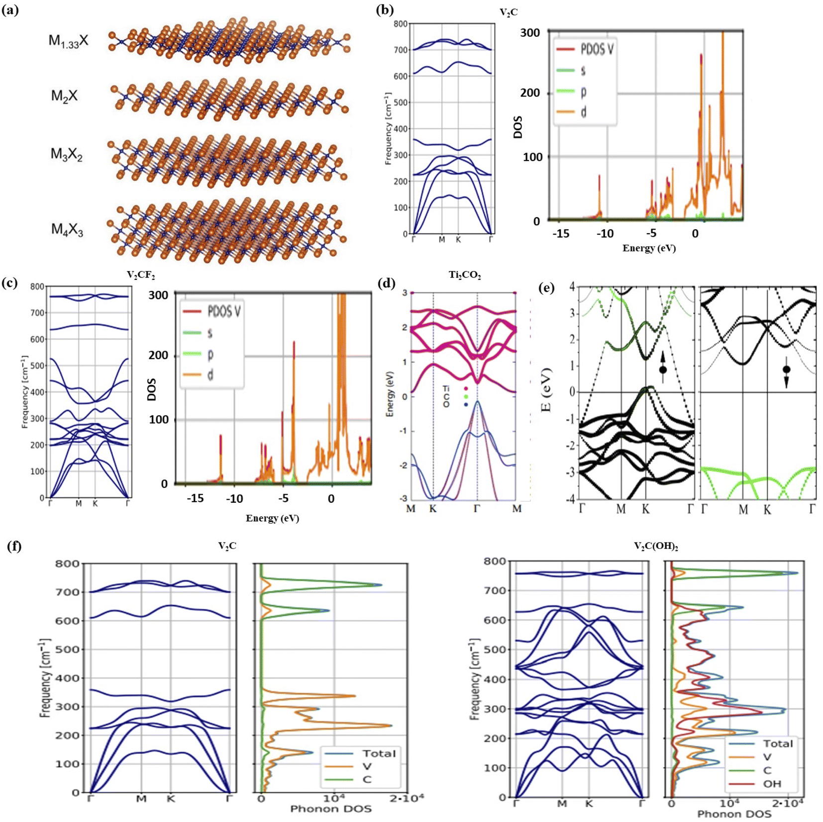 | ||
| Fig. 2 (a). The morphologies of various kinds of pristine MXenes.27. (b–d) The DOS structure of V2C, V2CF2 and Ti2CO2, respectively.34,35 (e) Electronic band structure and minority spin gap of first half-metallicity in Cr2C.29 (f) Phonon spectrum and DOS of conventional V2C and V2C(OH)2.34 | ||
2.2 Electronic properties of MXene
Generally, most of the MXene's nanostructure properties and electronic characteristics were calculated by using generalized gradient approximation (GGA) methodology.28 However, hybrid functionals also seemed to achieve a precise estimation of the electronic bandgap.29 It is anticipated that the pristine MXenes possess metallic characteristics. The M-d states, which are represented in Fig. 2b, are considered to contribute to the electrical conductivity in the MXene systems as they are located close to the Fermi level. The conventional MXenes are expected to have a greater charge carrier density of states (DOS) close to the Fermi level in contrast with their initial MAX phases.14 According to the composition of the M, X, and T atoms, MXenes' electrical characteristics can change from a metallic nature to a semiconducting nature after functionalization. While the bulk of terminated MXenes still exhibit metallic properties as shown in Fig. 2c for V2CF2, and semiconductor properties are predicted for different structures (such as Sc2CT2,28 Ti2CO2,28 Zr2CO2,28 Hf2CO2,28 Cr2CF2,29 Cr2C(OH)2 (ref. 29) and (M′2/3M′′1/3)2CO2 (M′ = Mo, W; M′′ = Sc, Y)30). This change is caused due to a shift in the Fermi level as shown in Fig. 2d for Ti2CO2. A direct band gap exists in Sc2C(OH)2, the only semiconducting MXene structure that does not possess an indirect band gap.2.3 Magnetic properties of MXene
Except for (Cr2Ti)AlC2,31 none of the Cr or Mn containing magnetic MAX phases (such as Cr2AlC, Cr2GeC, Cr2AlN, Cr2GaN etc.) have been etched into 2D MXenes so far. To achieve the desired ferromagnetic (FM) configuration, a few antiferromagnetic (AFM) configurations with numerous spin orientations between the transition metal layers and the non-magnetic (NM) configuration have been taken into consideration in spin-polarized calculations to determine the magnetic ground state of MXenes.32 In magnetic MXenes, half-metallicity has been predicted recently. Half-metallicity resulted in a conductivity entirely ensured by a single spin charge transport channel and a 100% spin-polarization of the electrons at the Fermi level.32 One spin-channel is insulating,33 while the other is metallurgical. First half-metallicity in Cr2C was anticipated by Si and colleagues,29 using the Heyd–Scuseria–Ernzerhof method to compute a significant minority spin gap of 2.85 eV as shown in Fig. 2e. In Ti2C and Ti2N systems, where true half-metallicity is only seen under biaxial strain, near-half-metallicity has subsequently been proposed.282.4 Vibrational properties
The determination of a system's phonon dispersion spectrum aids in confirming its thermodynamic stability and offers a comprehensive study of its thermodynamic characteristics. The estimated phonon spectrum of several terminated and pristine M2XT2 based MXene systems, where M denotes Sc, Ti, Zr, Mo, and Hf atoms; while X shows C, and N atoms; and T shows F and O termination groups, which indicate some unique stabilities. Fig. 2f 34,35shows the phonon spectrum and DOS of conventional V2C. Numerous characteristics of V2C systems are similar to M2C based MXene systems and even higher-order M3C2 and M4C3 based MXene systems, conserving the crystal structure and chemical bonding.36 Furthermore, the M elements, having low and high frequency vibrations, are separated by a substantial phonon band gap.2.5 Mechanical properties
The elastic constants (c11) of some of the pristine MXenes were previously identified by Kurtoglu and colleagues.37 It was observed that the elastic constants of 2D MXenes are typically twice those of their associated MAX phases. Nitrides are typically stiffer than their carbide counterparts as the N atoms give their extra electron in comparison to C atoms. Thus, resulting in the formation of stronger bonds between M–X atoms in nitride compounds.38 According to the c11 values, 2D transition metal carbides become more rigid as the M element's atomic mass rises. In addition, the presence of terminal groups also drastically reduces the c11 values of all MXenes. In general, the stronger MXenes are produced by the O-termination group system as compared with the –F and –OH termination group systems. This is because the O-termination group system possesses smaller lattice characteristics. MXene-based systems have a Young's modulus value of 330 + 30 GPa, which is higher than the highest known value for a solution-processed 2D nanomaterial. For instance, for MoS2 and graphene oxide, the highest reported Young's modulus values are 270 + 100 GPa and 210 + 20 GPa, respectively. However, MXenes' Young's modulus is lower than the values for graphene and h-BN i.e., 1000 + 100 GPa and 870 + 70 GPa, respectively. MXenes possess intriguing possibilities in composites with polymers, oxides, or carbon nanotubes because of their excellent characteristics such as higher bending stiffness, hydrophilicity, and negative zeta potential.3. 2D MXenes for energy conversion applications
In 1972 first photocatalytic device manufacturing has been discovered. Photocatalysis is a process in which solar light energy is converted to chemical energy.39 Several photocatalytic reactions, such as hydrogen generation by the dissociation of water molecules,40–42 carbon dioxide assimilation,43,44 and photocatalytic degradation of organic contaminants45–48 are aided by photocatalysts. Traditional transition metal oxides (TMOs) such as TiO2, BiOCl, BiOBr, and a combination of metal–organic structures like graphene-based carbon nitride and 2D nanomaterials having bandgap tunable properties like MXene and phosphorene, can all be classified as photocatalysts.49–51Recently, in photocatalysis, researchers showed interest in the synthesis of TiO2 nanocomposites utilizing 2D materials like graphene, MoS2, WSe2, and phosphorene. TiO2 nanocrystal nucleation and development can be facilitated by 2D materials with large surface areas. Furthermore, they also enhance the transmission of charge carriers induced due to solar light, which aids efficient solar energy conversion. When MXenes were combined with TiO2 nanocomposites, it demonstrated exceptional results for photocatalytic activities.52 MXenes nanosheet helps composite materials to conduct electricity more efficiently.53–55 The hybrid structure of MXene and TiO2 has numerous advantages. The first advantage is that oxygen surface terminal groups that can interact with Ti atoms, and the second is easy partial oxidation of Ti3C2 and Ti4C3, all due to the presence of Ti metal. As shown in Fig. 3a and b that by using the hydrothermal procedure, TiO2 can be produced at the surface of Ti3C2. Fig. 3c–f illustrated that TiO2 could be developed perpendicular to the [001] direction and also along with the Ti3C2 lattice fringes. From Fig. 3g it can be observed that TiO2 which has two different types of Ti–O–Ti bonds at the interface shows an equilibrium atomic configuration over the Ti3C2 surfaces using DFT calculations. Theoretically, the densities of states (DOSs) for these bonds have been depicted in Fig. 3h and i.
 | ||
| Fig. 3 (a). Transmission electron microscopy (TEM) diagram of combined MXene and Ti3C2/TiO2 interfaces nanomaterial.52 (b–d) Close image of the yellow highlighted inbox of TEM diagram shown in (a), (b and c) show Ti3C2 near TiO2 nanostructures. A comparable fast Fourier transform (FFT) image is shown inset in (c).52 (e) TiO2 developed perpendicularly to the MXene Ti3C2 nanolayered structure's [001] direction.52 (f) TiO2 developing at an MXene sheet's edge. The lattice fringes are seen in the insets.52 (g) DFT results which illustrate the initial and final atomic configuration structures of the interface. Here, Ti, C, O, and H atoms are denoted by cyan, black, red, and green balls, respectively. Ti1–O1–Ti2 and Ti3–O2–Ti4 are two Ti–O–Ti bonds with different PDOS analyses (h) and (i) respectively.52 | ||
Organic methyl orange (MO) dyes illustrated exceptional photocatalytic degradation performance. Fig. 4a shows the dye's concentration decay profile as a function of processing time. The photodegradation performance of the composite could be influenced by its synthetic circumstances such as hydrothermal temperature. The highest efficient rate was achieved at 160 °C in this situation.52 Moreover, the photocatalytic performance is also affected by the time taken to synthesize the TiO2/MXene hybrid composite structure as displayed in Fig. 4b. As a result, the best photo degradation rate can be produced by a 12 hour hydrothermal synthesis technique. This TiO2/MXene hybrid composite structure outperformed a commercial TiO2-based photocatalyst in terms of photocatalytic performance.56,57
 | ||
| Fig. 4 (a) MO photocatalytic deterioration on (001) TiO2/Ti3C2 at various hydrothermal temperatures. For the produced combined nanostructure of MXene and (001) TiO2/Ti3C2, the curve shows decreasing nature of MO dye concentration with time for distinct hydrothermal temperature. The inset figure shows the variation of photocatalytic deterioration rate constant (k) vs various hydrothermal temperatures for assembled hybrid nanostructure.52 (b) Variation between photocatalytic deterioration rate constant (k) and hydrothermal synthesis process duration for two different hybrid nanostructures i.e., (001)TiO2/Ti3C2 and particulate(p)-TiO2/Ti3C2.52 | ||
In addition to photocatalysis, MXenes could also be used for photovoltaic applications. A photovoltaic device is made up of a heterostructure which is a hybrid structure of two materials that serves as an interface for the separation of electron–hole pairs (EHPs) generated due to solar light. These photoinduced EHPs transmitted to the electrodes for the creation of photocurrent. For photoelectronic energy transformation purposes, MXenes possess unique features such as variable work functions, excellent electronic conductivity,58 and good optical transmissivity.59 Some specific surface functional groups strongly influenced the MXenes' work functions, for example, –OH and –O groups could reduce and raise the work functions value, respectively. Moreover, MXenes have an extensive range (2.14–5.65 eV) of work functions as compared to other materials. Consequently, an appropriate barrier height should be achieved by the metal/semiconductor junction for the generation of photoelectric current.60,61
When the MXene is stacked over silicon, a vertical heterostructure has been formed and the EHPs were created due to incident solar light. During light irradiation of 100 mW cm−2, a photovoltaic device comprising a combined MXene/Si heterostructure Schottky junction cell62 displayed an open voltage and a short circuit current density of 0.34 V and 12.9 mA cm−2, respectively. Since, this photoelectric cell has excellent sensitivity, enhanced ON/OFF ratio,63 and quick response time, hence, this type of photoelectric cell can be employed as a self-powered photodetector. In another example, the MXene (Zr2CO2) and blue phosphorene contact showed a minima of the conductance band (CB) and a maxima of the valence band (VB) from both MXene sides in the band alignment diagram. There was variation in the electronic band structure of semiconducting materials due to strain engineering,64 which may lead to spectacular photoelectronic applications.65–70 When some tensile strain was applied at the contact of the heterostructure, it showed band alignment between the minima of CB and maxima of VB from MXene and blue phosphorene, respectively. This heterostructure contact of MXene/semiconductor could open up new photoelectronic and photonic possibilities.
Electrocatalysts for hydrogen evolution reactions (HER) in hydrogen-energy technologies have gained a lot of popularity, and their practical use is inexpensive and plentiful. The efficiency of hydrogen generation and its uses is determined by the HER, which is a component of the electrochemical reactions in both green-energy and hydrogen-related technologies.71 The effective HER reactions are greatly influenced by the electrocatalyst used in these technologies. Due to their high HER catalytic efficacy, noble metals like platinum and palladium are currently the most widely used electrocatalysts in fuel cells and the electrolysis of water. To substitute for noble-metal catalysts, new electrocatalysts with cheap cost and high availability have been extensively studied. Due to their distinct physical and chemical characteristics, 2D nanosheets, such as MXenes and TMDs,14,72 have become increasingly popular as electrocatalysts. Pan et al.73 demonstrated a systematic study of the hydrogen evolution processes on MXenes (Mo2X and W2X, where X = C and N). Hydrogen adsorption patterns, composition, and surface functionalization all have a huge effect on efficiency of HER. Among all MXenes, the W2C monolayer exhibits the greatest HER activity with nearly low overpotential at high hydrogen densities. Hydrogenation can considerably enhance its catalytic performance across a broad spectrum of hydrogen densities; however, oxidation significantly reduces its activity. With careful adjustment of the experimental setup, it is quite possible to obtain outstanding HER performance on W2C monolayers with H atoms adsorbed on top of W atoms in the entire H-coverage range with very high efficiency. Nevertheless, when the W2C monolayer is oxidized or functionalized by oxygen atoms, particularly at a high H-coverage, its optimal HER activity got reduced. Moreover, it demonstrates that oxidizing Mo2X monolayers can greatly increase its HER activity. Because of almost zero Gibbs free energies, the oxidized Mo2X monolayers display the best HER performances in individual processes at medium H-coverage and in collective processes at high H-coverage. In order to keep the improved HER activity of the W2C monolayer used as an electrocatalyst, oxidation should be avoided while Mo2X monolayers need to be functionalized by oxygen to boost activity. By adjusting composition and functionalization, MXenes with activity similar to new metals may be produced, and hence registered its strong presence in HER reactions.
4. MXenes for wearable devices
In recent years, there is huge growth in the demand for wearable electronic devices, with applications in different areas such as fashion, gaming, smart glasses, gadgets using AR/VR a, and more importantly – healthcare.74–77 Blood pressure, physical activities, body posture, blood oxygen saturation level, and body temperature are some of the most common data analyzed using wearable healthcare devices.4.1 MXene-based wearable sensors
Wearable mechanical sensors can be classified into four types based on their sensing mechanisms: resistance-type, capacitance-type, piezoelectric-type, and triboelectric-type sensors. Among all types of sensors resistive and capacitive type sensors have various advantages such as easy fabrication and easy signal gathering capabilities in resistive sensors, low hysteresis, and high linearity in capacitive sensors.78,79 MXens are widely used materials for developing flexible resistive and capacitive sensors. In these sensors, the applied force can be converted into a resistive or capacitive type signal via flexible strain/pressure sensors. In flexible capacitive-type sensors, the dielectric layer is sandwiched between two conductive layers, and when external hindrance is applied the surface area of both conductive plates as well as thickness of dielectric also vary due to which there were changes occurred in the capacitance value.80Some essential metrics or figures of merits, such as sensitivity, sensing range, and response time, have been used to assess the quality and performance of wearable strain/pressure sensors. Moreover, the gauge factor (GF) of strain sensors can be determined by the proportional changes in the slope of capacitive or resistive signals related to the exterior strain on the sensors. For resistive-type sensors the GF is defined as GF = (R − R0/R0)/ε and similarly for capacitive-type sensors GF is defined as GF = (C − C0/C0)/ε81,82 where, ε is strain, C0 & R0 are capacitance and resistance without strain, respectively, and C&Rare capacitance and resistance when the sensor is elongated to different strains. And the sensitivity of pressure sensors is given by the relation; S = (R − R0/R0)/ΔP. Here,ΔP is the proportionality change of pressure loading.83
4.2 MXene-based wearable strain sensors
Wearable strain sensors could benefit from MXene-based composites, which have good electrical conductivity and flexibility. MXene fibers, textiles, films, and gels are all examples of MXene-based composites that have been extensively studied and published in a pioneered research paper.Flexible MXenes are utilized in strain sensors except for fabric-derived MXene composites. A hybrid of MXene/CNTs was synthesized by the layer-by-layer spray coating technique (Fig. 5).84 Here CNT's acted as a catalyst between nanosheet layers of MXene. And to condense MXene/CNTs films with electrodes, a wearable device was fabricated by employing elastic latex rubber. A skin-fasten-on sensor with a very low detection limit (0.1%), a GF of 772.60, and a variable detection range of 30–130% in strain has been provided by using the sandwich-like structure of MXene/CNTs. Yang et al.85 equipped MXene/graphene hybrid film as sensing material by employing vacuum filtration. All the conductive film was transferred to stretchable polydimethylsiloxane (PDMS) substrates so that they could be assembled into a strain sensor. The sensing mechanism of MXene/graphene/PDMS as a sensor is shown in Fig. 6. Here, the entire strain on the sensor was divided into two layers. It was noticed that the coordinated motion of these two layers balanced the destruction and managed the conductive path ensuring the high GF (190.8 and 1148.2) of the sensor within its working range (0–74.1%). Yang et al.86 also approached similar steps to fabricate nanoparticle-nanosheet of other MXene as a hybrid film for stains sensor. These nanoparticles and nanosheets played a significant role via mechanism of constrained micro rack propagation path which in turn improved the sensitivity and detection range of the device. After employing PDMS, desirable results were achieved in the strain sensor such as a GF over 178.44, a working range of 0–53% with a detection limit as low as 0.025%.
 | ||
| Fig. 5 The fabrication method of MXene/CNTs combined nanostructure.84 | ||
 | ||
| Fig. 6 Schematic illustration of strain sensor based on MXene Ti3C2Tx/graphene/PDMS combined nanostructure for distinct stretching states.87 | ||
4.3 MXene-based wearable pressure sensors
In wearable piezo resistance-type pressure sensors, Mxene-derived composites were proved to be the potential candidates. To design the sensing material, where resistance changes with the change of external pressure, piezo resistance type pressure sensors are needed. For developing flexible pressure sensors, MXene is mixed with polymer as a conductive filler. Chen et al.88 equipped MXene/single-walled carbon nanotube (SWCNT)/polyvinylpyrrolidone (PVP) composite film via solvent evaporation process. As shown in Fig. 7a 1D SWCNTs created anisotropic packages, MXene nanosheets formed membrane or lamellas, and PVP served as an adhesive during the manufacturing process. A tactile sensor was manufactured by combining the face-to-face hemisphere bumps after printing this novel hierarchical dendritic membrane or lamellar hybrid matrix using the rubber substrate. The assembled sensor has excellent performance parameters such as higher sensitivity of 165.35 kPa−1, a low detection limit of 0.69 Pa, and a stable cycling performance of 10![[thin space (1/6-em)]](https://www.rsc.org/images/entities/char_2009.gif) 000 times.
000 times.
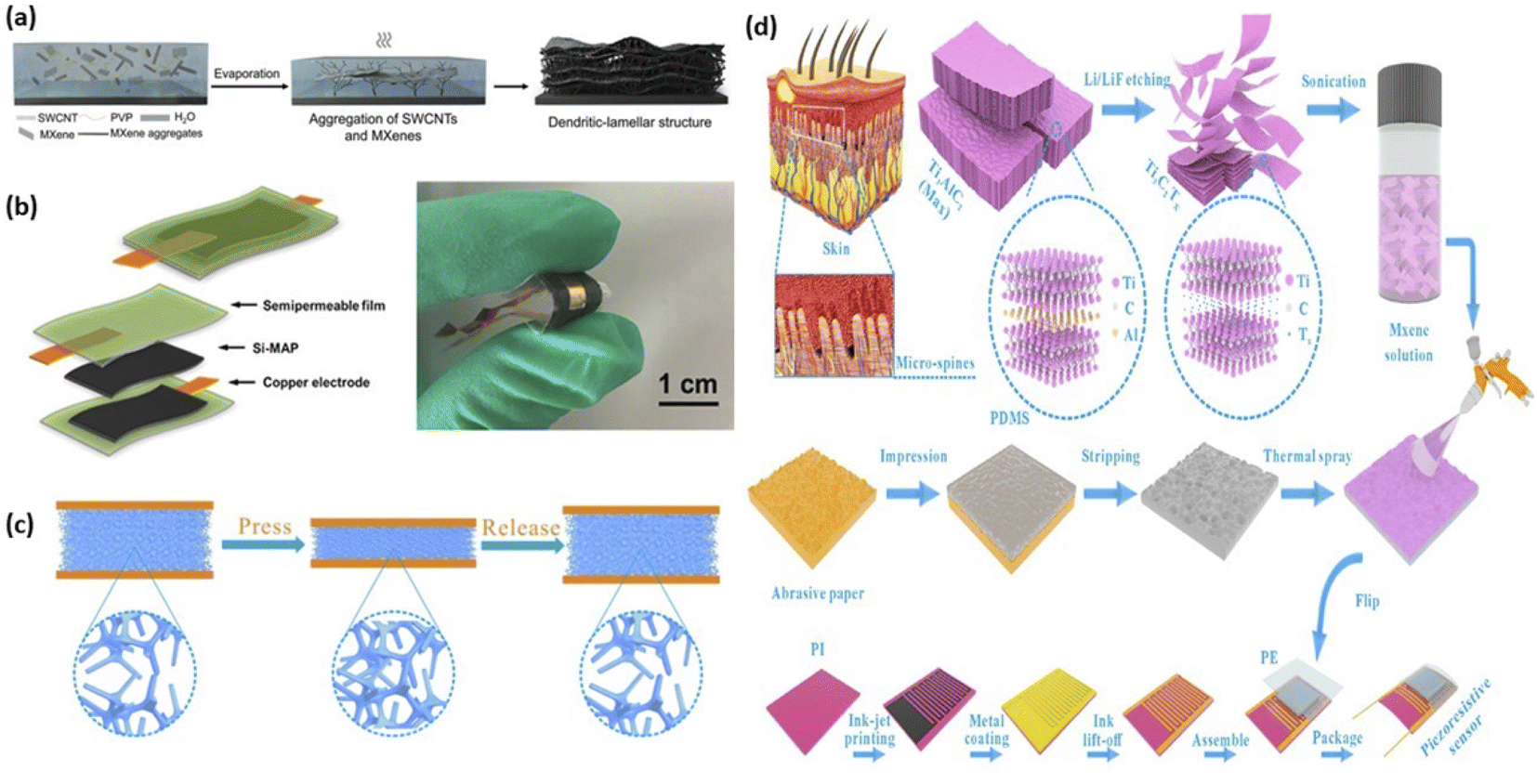 | ||
| Fig. 7 (a) The MXene/SWCNT/PVP dendritic-lamellar thin film synthesis process is depicted schematically.88 (b) MXene-decorated air-laid paper (Si-MAP) based flexible pressure sensor synthesis process is depicted schematically.90 (c) Schematic diagram of MXene-sponge sensor showing microfibers spacing reduced on exerting pressure.92 (d) The fabrication process of MXene piezoresistive sensors has a bionic spinous microstructure.96 | ||
A 2D or 3D nanostructure can also be fabricated by using MXene having excellent electrical properties such as higher conductivity and sensitivity. Li et al.89 described the fabrication method of MXene-coated cotton textile by using a dry method and dip-coating technique. The fabricated sensor consisted of a substrate having a wavy network-like structure and MXene having excellent electrical characteristics showing a quick response time i.e., 26 ms, higher sensitivity of 12.095 kPa−1 for 29–40 kPa and 3.844 kPa−1 below 29 kPa and high stability over 5600 cycles. As MXene-textile sensor was a promising candidate for wearable devices such as for detecting real-time human activity, wrist-pulse recognition, and finger motion detector like bending or touching. Ma et al.90 described the preparation of MXene-based air-laid paper (Fig. 7b) and its application as a pressure-sensitive device. The encapsulation by using a semipermeable (SPM) layer increased the device's durability and mechanical strength.
The wearable pressures sensor prepared by combining MXenes with the tissue paper91 has a moderate detection limit i.e., 10.2 Pa, and high sensing range i.e., up to 30 kPa, due to the virtue-of tissue paper's rough surface. Moreover, MXene-paper transient sensor was biocompatible and environmentally friendly due to encapsulation layers provided by using degradable poly lactic acid (PLA) sheets.
Furthermore, the 3D compressible substrate is commonly made of an inexpensive, and porous sponge. Yue et al.92 have illustrated a conductive MXene sensing element which was wrapped sponge along with insulated PVA. Initially, there was much void space left out for air between microfibers as illustrated in Fig. 7c. When an external force is applied on the surface of the MXene-sponge sensor, this leads to a decrease in the space between fibers. Consequently, this process decreases the air space and increases the number of conductive points. Besides, when the load was removed from the surface of the sensor, the sensor gains its original shape and there was a decrease in the number of conductive points. As a result, a variation in external force induces a change in MXene-sponge structure (change in sensor's resistance), which lead to a change in the current signal. This assembled MXene-sponge pressure sensor showed higher sensitivity of 147 kPa−1 for 0–5.37 kPa and 442 kPa−1 in 5.37–18.56 kPa.
Moreover, compressible and flexible nature 3D MXene-aerogel pressure sensor had been fabricated with the help of the directional freeze-drying method. Chen et al.93 used the combination of MXene and bacterial cellulose (BCL) to create a carbon aerogel pressure sensor. The elastic nature of carbon aerogel with continuous and organized wave-shaped structure was created after passing through different processes i.e., freeze-casting, freeze-drying, and at last annealing methods. The creation of parallel membrane or lamellas was aided by hydrogen bonding between hydroxyl-rich BCL and MXene, which confirmed the stable structure (>100000 cycles) of the carbon aerogel and provided it super mechanical strength, excellent compressibility, elasticity, and fatigue resistance. The assembled MXene-BCL carbon aerogel sensor has a sensitivity of 12.5 kPa−1 over a wide range of 0.01–10 kPa. Additionally, in the same way by combining MXene and cellulose nanocrystals (CNCs), a flexible/compressible structure of carbon aerogel was designed.94 The lamellar structure created by the combination of MXene and CNCs has significant advantages as CNCs provided mechanical strength such as dispersing, nano-supporting, and reinforcing to the designed structure.
External signals and disturbances are detected by the human epidermis, which is an excellent sensor. A series of MXene sensors have been developed that are influenced by human skin. Wang et al.95 described a flexible pressure sensor by the combination of MXene and natural microcapsule (NM). External pressure stimuli were expanded and conveyed by replicating the interlocking microstructures between the cutaneous and epidermic layers of human skin, resulting in improved sensing properties for the MXene/NMC pressure-sensitive sensor. The designed sensor had excellent characteristics i.e., a low detection limit of 8 Pa, a quick response time of 14 ms, and outstanding cycle stability after being assembled (5000 cycle number). As illustrated in Fig. 7d, Cheng et al.96 designed a MXene based pressure sensor that utilized abrasive paper as a template having arbitrarily dispersed spines that were influenced by human skin micro-spines. The sensitivity of this biomimic sensor was 151.4 kPa−1 and the detection limit was 4.4 Pa which shows outstanding results.
5. MXenes for electrochemical energy storage
5.1 MXene-based electrochemical batteries
In general, energy conversion and storage technologies use electrochemical reactions for centuries using carbon-based materials i.e., graphite.97–99 Since, enormous physical and electrical properties including larger specific surface areas, higher electrical conductivity, as well as outstanding mechanical properties of carbon materials, such as fullerenes,100–102 carbon nanotubes,103–106 and graphene107–110 were due to recent breakthroughs in sp2-hybridized in the carbon atom, have improved electrochemical performance. After carbon-based materials like graphene, the other 2D nanomaterials with promising energy storage potential, such as TMDs111–114 and phosphorene,115–118 have also attracted researchers' attention.Nowadays, secondary batteries (SBs) and supercapacitors (SCs) are the most common energy storage methods. SCs store energy in electrochemical form and delivers energy due to adsorption and desorption of reversible ions near the electrode–electrolyte interface. SCs were used in mobile applications and electric vehicle power sources because it has phenomenal features such as high output power and quick charge–discharge rates.119–125 The present research interest in hybrid-powered autos, divesting a major portion of the market due to reduction in carbon emissions. These demands sparked a lot of interest in research towards low-cost, and long-cycle-life batteries.
Conventional metal-ion batteries suffer from poor performance due to lower energy density. MXenes are used for developing large capacity and high-power battery electrodes, improving the energy density by more than 30% as compared to lithium-ion batteries. The change storing capacity of MXenes depends on formula weights and surface terminations. For instance, M2X MXenes possess higher energy storing capacity as compared to the M3X2 and M4X3 MXenes due to their lower formula weights.126 Moreover, oxygen surface termination proved to be more promising for energy storing an application, while the other kinds of terminations such as hydroxyl and fluorine restrict the lithium-ion movement resulting in lower storing capacity.127
Several strategies have been adopted to boost the storage performance of MXenes-based batteries through mixing MXenes with other materials and improving electrode architecture. Ren et al. have mixed 2D Ti3C2Tx MXene with carbon nanotubes (CNTs) to improve the storing capacity of MXenes significantly as compared to pristine MXene.128 The hybrid structure showed a very high storing capacity of 1250 mA h g−1 at 0.1 C due to the adsorption of Li ions on the edges of MXene flakes. MXenes could also work as a promising electrode material even for non-lithium-ion batteries. Xie et al. have used MXene nanosheets for non-lithium-ion battery anodes by theoretical and experimental techniques.129 They observed that pristine MXene showed superior performance as compared to the oxygen terminated MXenes.
5.2 Supercapacitors
Supercapacitors are classified into three varieties based on differences in the charge storing medium. These three types of supercapacitors are electrical double-layer capacitors (EDLCs),130–134 pseudo-capacitors,135–141 and asymmetrical supercapacitors (which is a combination of one EDLC electrode and a pseudo-capacitive electrode),142,143 as shown in Fig. 8. A hybrid capacitor has been recently introduced, which has two symmetrical electrodes. These electrodes are made of materials used in battery cathodes. The electrical energy is stored in EDLCs by using the electrodes constructed of carbon-related materials. The charge storage is due to quick ion adsorption at electrodes by many pores via a physical electrosorption technique. | ||
| Fig. 8 Different categories into which supercapacitors can be divided.144 | ||
MXenes outperform other materials in developing supercapacitors.145–147 The usage of mesoporous MXene sheets in supercapacitors has been supported by a progressive report. Since, at the scan rate of 10 V s−1, the value of specific gravimetric capacitance and volumetric capacitance for MXene hydrogels148 (having 3 mm Ti3C2TX film) were 380 F g−1 and 1500 F cm−3, respectively. These results are equivalent to those obtained with RuO2 in commercial supercapacitor electrodes.149–153
 | (1) |
As there were variations in specific surface areas of electrodes, consequently capacitances of EDLCs changed. The theoretical capacitance of double-layer supercapacitors is finite and exclusively governed by their physical properties, such as specific area. The significant resistance due to ions present in the porous carbon structures slows double-layer supercapacitors charging and discharging rates. Some examples of carbon electrodes are porous carbon, mesoporous carbon, carbon aerogel, graphene, and so on. The specific gravimetric capacitance, volumetric capacitance, energy and power density of commercial capacitor with graphene thin films are 78 F g−1,155,156 198 to 736 F cm−3,157,158 62.8 to 136 W h kg−1159,160 and 7.2 to 500 W kg−1,161–163 respectively.
| Ti3C2Ox(OH)yFz + ∂e− + ∂H+ = Ti3C2Ox−d(OH)y+∂Fz | (2) |
By utilizing Faraday's law, the maximum theoretical capacity for the redox reaction of Ti3C2O0.85(OH)0.06F0.26 and 0.85e is 1200 F g−1 or 615C g−1. Initially, when ions accumulate on a 2D metal and electrolyte junction and potentials are greater than their reversible redox potential (for example, H+ on Pt as well as Pd2+ on Au),165 this process is known as underpotential deposition. Redox pseudocapacitance occurs in a faradaic redox structure (such as RuO2, MnO2, and some conducting polymers) when a portion of the transformation of reduced ions is electrochemically absorbed at the surface or adjacent to the surface of oxidised elements as well as its vice versa is also true. Finally, the intercalation pseudocapacitance, in which ions are intercalated in-between a redox-active material, takes place on a timescale similar to that of an EDLC without undergoing a crystallographic phase transition.166
In recent years, the electronically conducting polymer (ECP) based asymmetric supercapacitors has attracted a huge amount of researchers' interest. They are formed when p-doped ECP and activated carbon (AC) are applied at the positive and negative electrodes, respectively. The challenge of finding a robust n-doped ECP electrode material is removed by this design. In order to function in non-aqueous electrolytes, a number of ECPs, such as poly(3-methylthiophene) (PMT), poly(4-fluorophenyl-3-thiophene) (PFPT), and poly(3,4-ethylenedioxythiophene) (PEDOT), and Polyaniline (PANI), have been investigated in detail as ECP-AC asymmetric hybrid devices. Since each electrode has a different specific capacitance and potential variation band, adjusting the ratio of negative to positive electrode material in terms of capacity instead of weight is a crucial parameter for the performance of asymmetric devices. As the majority of the voltage fluctuation will take place across the AC, i.e., the negative electrode, the asymmetric device will display an almost linear charging–discharging profile. In contrast, a much more battery-like charging–discharging profile is seen when the AC electrode's capacity is greater, which is an indication of the ECP's redox activity.
A significant effort is currently being made to raise supercapacitors' energy density to achieve a target range of around 20–30 W h kg−1. Numerous studies have been conducted to boost the energy density of EDLC based supercapacitors. There are primarily three methods to enhance the performance of supercapacitors: (1) by using different electrode materials possessing enhanced capacitance such as carbon or redox materials, (2) by altering the electrolyte either by using a substantial new electrolyte or ionic aqueous solution, and (3) by creating hybrid capacitors. By combining redox-active materials (such as graphite, metal oxides, and conducting polymers), several hybrid capacitor devices are feasible. In the case of hybrid capacitors, both electrodes are a combination of capacitive and battery-type electrodes. Supercapacitors typically have a capacitance that is irrespective of potential while scanning potential. Because the current is relatively constant during the charging–discharging processes, the cyclic voltammogram (CV) curve of a supercapacitor should keep its rectangular shape.
Evident faradaic maxima and charging–discharging peaks are possessed in the CV and galvanostatic charge/discharge (GCD) profiles for a battery using both electrodes. In contrast, the two electrodes of an asymmetric electrochemical capacitor exhibit excellent capacitive qualities, leading to an ideal CV graph that is rectangular in form and a GCD graph that is triangular in shape. By utilising eqn (3) to assess the charge-storage capacity at a particular voltage, the capacitance, C, may be computed.
| C = ΔQ/ΔU | (3) |
The CV and GCD profiles of the entire device can display more capacitive-like behaviour with noticeable divergence from conventional capacitive properties, even when one electrode behaves as a battery type electrode with noticeable anodic and cathodic maxima characteristic in CV profile. Estimating the hybrid capacitor's electrochemical behaviour by using eqn (3) will lead to inaccurate results. In this situation, the equation needs to be changed and given as:
 | (4) |
In eqn (4), “t1” refers to the period following the initial voltage drop, “t2” to the point at which the discharge is complete, and “I” refers to the continuous current provided to the supercapacitor.
6. MXenes for chemical detection
Among various potential applications of 2D materials, gas sensing has rejuvenated over the last decades, driven by very high sensitivity, selectivity, and rapid response. Graphene led the ever-increasing list of theoretical and practical experiments by successfully detecting even a single gas molecule on its surface.167 However, its slow response and poor selectivity forced the researchers to find out other 2D materials. MXenes possess several promising electronic properties which could be exploited for gas sensing applications. In addition to a very high surface-to-volume ratio, MXenes also possess high conductivity, and controllable surface chemistry making them suitable for high-performance gas sensors.17,168In recent years, different MXenes like Ti3C2Tx,16,17,169–175 Ti3C2,176–178 Ti2CTx,179 V4C3Tx,180,181 and Mo2CTx182,183 are utilised for the recognition of different gases, volatile organic compounds (VOCs), and humidity. Due to its exceptional characteristics, Ti3C2Tx is the most extensively used MXene as a gas sensing material. For various gases and VOCs, the MXenes sensing capabilities has been investigated, and consequently, it was discovered that MXenes were extremely sensitive to NH3,169–171,176,183 acetone,180 ethanol,17,184 NO2, methane,179 and humidity.172–174,177,178 Besides, MXene has been less investigated for the gases such as toluene,182 NO2,16 and H2.181 Eunji Lee et al. described the first MXene-based gas sensor, by using the hybrid structure of MXene and 2D-Ti3C2Tx nanosheets to investigate the sensing response towards ethanol, methanol, acetone, and ammonia-like gas molecules. It was observed that for the p-type Ti3C2Tx the sensing responses were due to its active defective sites and interactions of gas molecules with surface functional groups. Since, Ti3C2Tx had high adsorption energy for NH3 resulting in the strongest response i.e., ∼0.21/100 ppm.170
It could also be observed that when MXenes were combined with p-type semiconductors, the hybrid nanostructure revealed a positive gas response, in which the device's resistance increases when a reducing gas analyte is added.17,171,180 The sensing performance is greatly influenced by the thickness of the MXene film. Generally, the sensing response of the device decreases with both nature of gases (reducing and oxidizing) as the thickness of MXene nanosheets increases. The gas sensing characteristics of MXenes are also influenced by their composites, structure, and manufacturing process. At room temperature, alterations in carbon nanomaterials (such as graphite, TiC, lampblack, and so on169) and Ti3C2Tx flake morphology171 directly affect the NH3 sensing response. And it was observed that due to shorter gas diffusion paths smaller flakes showed better sensitivity as compared to the bigger ones.169,171 Kim et al.17 revealed that the Ti3C2Tx thin film was employed as a metallic channel which provides excellent electrical conductivity, resulting in low noise and high signal transmission caused by enormous adsorption sites for ethanol sensing.
From the DFT calculations, Ti3C2(OH)2 and Ti3C2O2 exhibited the highest binding energy abilities towards hydrogen bonding gases such as acetone and NH3 in contrast with acidic gases as shown in Fig. 9a. In addition, Ti3C2Tx exhibited the lowest signal-to-noise ratio (SNR) i.e., 0.005% in contrast with other 2D nanomaterials such as black phosphorus, MoS2, rGO, etc. as illustrated in Fig. 9b,17 due to its low value of electrical resistance. By using DFT first-principles calculations, for single-layered Ti3C2Tx the selectivity and sensitivity were higher for NH3 at room temperature. As illustrated in Fig. 9c and d, the NH3 has dominant characteristics i.e., the higher negative adsorption energy, charge transfer, and smaller molecule size in contrast with other gases.176 The strong binding interaction between N and Ti atoms of NH3 and Ti3C2O2, respectively, contributed to the higher adsorption of NH3 molecules.176
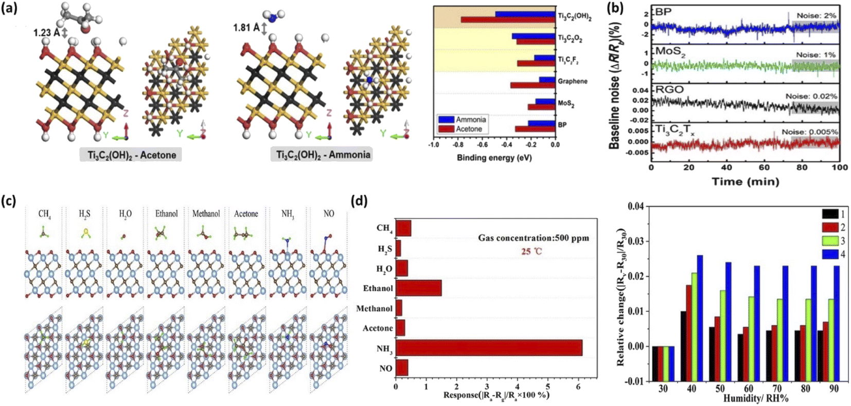 | ||
| Fig. 9 (a) Simulation findings of absorbed gas molecules on different 2D materials using the density functional theory calculations. The binding energies of acetone and ammonia for various sensing materials (such as Ti3C2(OH)2, Ti3C2O2, Ti3C2F2, graphene, MoS2, and BP) are depicted.17 (b) The electrical noise of different sensors upon N2 exposure.17 (c) Ti3C2O2 surface highest stable configuration for several absorbed gases, seen from the side and top.176 (d) Selectivity study of different gases (such as CH4, H2S, H2O, ethanol, methanol, acetone, NH3, and NO) of Ti3C2 based MXene sensors at 25 °C and changes in relative resistance due to environmental humidity for varying layers of the sensor.176 | ||
Cho et al. described two different types of molybdenum carbide phases i.e., α-MoC1−x and β-Mo2C which possess higher porousness and metallic properties, owing to the distinct density of states (DOS) localization. α-MoC1−x MXene has a nanorod structure of 70–89 nm width, and β-Mo2C MXene has nanoparticle morphology with 200 nm diameter. These nanostructures exhibit exceptional physical and chemical characteristics, resulting in higher sensitivity, and the lowest detection limit (LOD). The sensitivity for α-MoC1−x was 15.1% of 5 ppm of NO2 gas molecule, LOD was 0.125 ppm, and higher stability at room temperature.183 Moreover, β-Mo2C showed no response for lower concentrations of NO2 and only responded to NO2 at a concentration level of 1 ppm with a 0.3% response. Since, MXenes have a higher oxidation rate, which impedes the electronic characteristics of nanomaterials during prolonged storage in the presence of water or humidity, leading to the transformation of titanium carbide (TiC) to oxidized state TiO2 i.e., titanium dioxide. Furthermore, the oxidation process could be controlled by either keeping MXene in an argon-filled container at a low temperature i.e., less than 5 °C (at the dried freezing condition), or dispersing in isopropyl alcohol (IPA). This process slows down the oxidation rate and the issue can be considerably mitigated. Chae et al. attempted to resolve the issue related to the oxidation of the MXene aqueous solution. They aged an aqueous solution of Ti3C2Tx for varying intervals of time, 5 and 10 weeks, and keep this solution at distinct temperatures i.e., 5 °C, −18 °C, and −80 °C. The sensing response outcomes for 5 ppm of NO2 were identical for as-synthesized and aqueous solution kept at −80 °C for 5 weeks of Ti3C2Tx. These results implied that the Ti3C2Tx flakes oxidation stability may be retained by using the same storage conditions.16 Because Ti3C2Tx gets oxidized straightforwardly with TiO2 in an oxidizing environment, it is more extensively used for gas sensing having a reducing nature than oxidizing gas detection. At ambient temperature, Jian et al. investigated the sensing properties of Ti3C2Tx for both reducing gases i.e., CO and NH3, and oxidizing gases i.e., NO2. Consistent response–recovery curves were obtained for both reducing and oxidizing nature gases. However, in the case of NO2 sensing, there was a considerable shift in the resistance baseline of the sensor. This irreversible NO2 performance issue could be attributed to Ti3C2Tx oxidation in an oxidizing environment.
Moreover, some different types of VOCs (like acetone, ethanol, and toluene) were also tested to check how MXenes respond to them. The performance of newly discovered MXene, V4C3Tx was evaluated for sensing acetone which shows excellent results at ambient temperature i.e., low detection limit and higher selectivity.180 Many VOCs react with MXenes having surface functional groups such as O and OH, and Mo based MXenes have more chemical activity than Ti-based MXenes, leading to increased gaseous contact and excellent sensing performance. Guo et al. investigated the toluene sensing ability of Mo2CTx and observed an excellent sensitivity and LOD of 0.0366 ohm/ppm at 140 ppm and 20 ppb, respectively.182 For the recognition of nonpolar gases at ambient temperature, a V2CTx-based sensor was constructed with the help of a flexible polyimide substrate using a simple drop-casting technique. Principal component analysis (PCA) was utilized to differentiate the VOCs. The ethanol content was detected with 93.4 percent accuracy, demonstrating the possibility of detecting a specific VOC in a complicated interfering VOC mixture.184
Dramatic improvement in the gas sensing ability of MXenes has been observed through Schottky barrier modulation at the semiconductor and metal electrode interface. Choi et al. have reported one such improvement by changing the barrier at the MXene/TiO2 heterointerface.185 The MXene/TiO2 hybrid was formed by oxidizing the MXene nanosheets (Ti3C2) for 4, 8, and 24 hours. By forming the hybrid, they recorded an improvement of 13.7 times as compared to pristine MXene upon exposure to NO2. A Schottky barrier is formed at the interface between MXene (metallic) and TiO2 (semiconducting) after making physical contact. Upon NO2 exposure, the barrier height increases due to the upward shifting of the potential barrier. Hence, the resistance of the device got increased as NO2 molecules captured the electrons from the surface and modulated the Schottky barrier height.
For developing high-performance gas sensors, heterojunctions are undoubtedly the preferred choices because of their easily tunable surface chemistry as it affects the catalytic performance and functional properties of the devices. MXene based hybrids have widely been used for detecting several hazardous gases including NO2, and NH3 gas analytes. He et al. have demonstrated a room temperature based MXene/SnO2 gas sensor for detecting NH3 gas molecules.186 The chemoresistive-type sensor should an excellent sensitivity of 40% upon 50 ppm of NH3 exposure. The improved sensing ability was ascribed to charge transfer between MXene and SnO2 nanoparticles due to their different Fermi levels. Moreover, the good conductivity of MXene at room temperature and its selective response toward NH3 facilitate a stable response. Wang et al. have exposed the superior sensing ability of MXene/ZnO hybrids for detecting NO2 gas molecules.187 A very high sensing response of 346% was obtained even at room temperature upon exposure to a very small concentration (200 ppb) of NO2 molecules. The hybrid showed a detection limit as small as 0.2 ppb with high selectivity. The MXene functionalization and efficient charge carrier separation at the interface due to UV activation play a major role in improving the sensing performance of the device.
7. Biomedical engineering
MXenes can also be used as bioimaging contrast agents. Photoacoustic (PA), fluorescent, CT, and MR imaging are advanced bioimaging techniques of MXenes. The penetration constraint of general optical imaging will be overcome by PA imaging. It is done by capturing the induced pressure waves of tissues during laser irradiation, allowing it for real-time observation of biological functioning, molecular, and structural characteristics. As a developing imaging technique, PA imaging has been employed for a variety of biomedical applications, including surgical assistance, medicine delivery, disease diagnosis, and treatment.188 To obtain substantially better PA signals in contrast to the underlying tissues, effective PA imaging contrast agents with superior photothermal conversion potential are required. However, their exfoliated MXenes nanosheets exhibited semimetal-likewise energy band structures, but the typical MAX phase possesses metal-likewise properties, allowing localized surface plasmon resonance (LSPR) phenomenon to occur depicting excellent absorption and superior transformation effectiveness under wide spectral light irradiation.189 As a result, combined structures of MXenes like Ti3C2 and Ta4C3 are extremely interesting for PA imaging and have a high photothermal conversion potential.190,191MXenes possess outstanding properties such as intense and wide absorption spectra in the near-infrared range (NIR), making them attractive for deep-tissue PA imaging. Several MXenes including Ta4C3,191 Ti3C2,192 and MnOx/Ti3C2 (ref. 190) have been investigated in vitro and in vivo PA imaging using NIR laser spectra. In recent years, the V2C MXene combined nanostructure has shown considerable promise in PA imaging. A unique green delamination approach based on algae extraction was developed by Zada et al. that yielded 90 percent V2C MXene nanosheets. This method helps to overcome the constraints of V2C MXene combined nanostructure such as low photothermal conversion capacity, harsh fabrication conditions, and so on as used in PA imaging.193 In vitro and in vivo systemic-based tests, the resulting V2C MXene assembled nanosheets showed exceptionally robust photothermal absorption in the NIR area and robust PA signals for PA imaging-guided cancer treatment. Furthermore, as shown in Fig. 10a by using a simple top-down technique Shao et al. synthesized titanium nitride (Ti2N) quantum dots (QDs) with a diameter of about 5 nm.194 The produced Ti2N QDs had a remarkable PA effect due to their extremely high photothermal transformation efficiency during laser irradiation in the first and second NIR windows as shown in Fig. 10b. As shown in Fig. 10c and d with the help of in vitro systemic test the PA signals showed a clear linear variation with Ti2N QD concentration. After pre-set time intervals mice having tumors had given Ti2N QDs through veins, and then the tumor tissues' PA pictures and signals were obtained. After treatment in the initial stage of circulation the PA signals (within the tumour tissues) soon enhanced. This is due to the quick collection of Ti2N QDs using enhanced permeability and retention effect as shown in Fig. 10e and f. The PA signal strength attained its highest value after four hours administration, showing high PA visuals for tumours, as displayed in Fig. 10g.
 | ||
| Fig. 10 (a) PA imaging-guided photothermal therapy (PTT) using biodegradable Ti2N Quantum Dots (QDs) in first/second bio-windows (NIR-I/II) are depicted schematically. Using multiple control groups (such as skin, water, blood, and tissue of mice).194 (b) PA pictures in NIR-I/II using 808 nm and 1280 nm laser irradiation.194. (c and d) PA and their correlated signal sensitivities diagrams for Ti2N QDs solutions having varied concentrations level from 0 to 500 ppm.194 (e and f) Depicts the PA images and correlated signal strength after injecting the injection into tumor tissue (at the tail vein).194 | ||
MXenes have diverse characteristics due to their distinctive reconfigurable layered structures and changeable elemental composition, which improve their medicinal uses, including traditional drug administration, photodynamic treatment, and synergistic treatments. MXene-based combined nanostructure materials have been studied for a variety of therapeutic purposes. The most effective way for achieving intended drug administration and reducing undesirable effects in patients is to use drug administration systems.195 MXene-based biocomposites material provided numerous advantages for building drug delivering systems as innovative 2D biocomposites material. The first advantage was that the unique lamella structure MXene based bio-nano materials offered a huge specific surface area. These properties of MXene based bio-nano materials provided plentiful attachment sites and enormous reservoirs for efficiently storing and releasing therapeutic compounds. The other benefit is after injecting intravenously these MXene-based nanomaterials disperse rapidly and collect within tumor locations during cancer treatment. Additionally, MXene-related bio-nano materials possess excellent physical, chemical, electronic, and optical characteristics.
The drug administration system including bioimaging and therapeutic modalities could be converted to a smart drug administration system using the unique properties of MXenes.196 Doxorubicin (DOX) is a powerful chemotherapeutic (CTA) medication that is frequently used as a model drug in nanoparticle-based medicine-related research. As shown in Fig. 11a, Han et al. have synthesized atomically thin Ti3C2 MXene nanosheets with soybean phospholipid (SP) alteration as a drug transporter for storing and administering DOX, as well as a synergistic cancer treatment.197 The drug-loading effectiveness of Ti3C2 MXene combined nanostructure was as high as 211.8% due to an ionic coupling between the positively and negatively charged site of DOX and Ti3C2-SP nanomaterial sheets. Moreover, pH-based and NIR laser-triggered on-requisition drug delivery was observed in Ti3C2 MXene combined nanostructure as shown in Fig. 11a. As shown in Fig. 11b, Ti3C2-SP combined nanostructure was found to be able to enter tumor cells through endocytosis and liberate the encapsulating DOX in an acidic intracellular milieu. DOX@Ti3C2-SP combined nanomaterial sheet outperformed in contrast with pure DOX in terms of cancer cell death, which is likely because Ti3C2 MXene's combination possess better cellular endocytosis as a transporter.
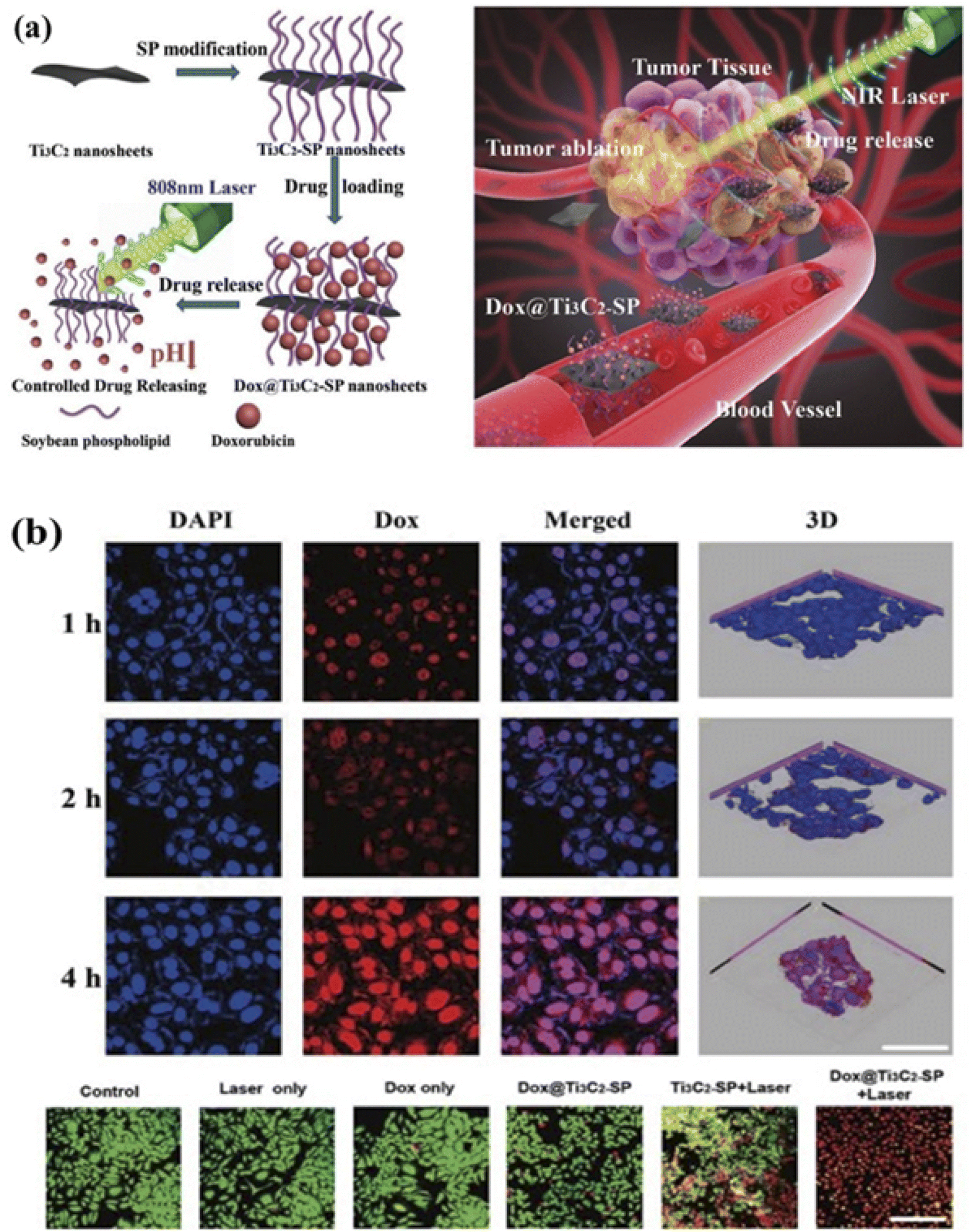 | ||
| Fig. 11 (a) Schematic drug loading and releasing on Ti3C2 nanosheets, and its surface modification by utilizing soybean phospholipid (SP) during inner or external laser excitation. The inset figure shows Transmission inside the blood vein, accumulation into the tumor, controlled drug release, and NIR-triggered photothermal ablation of tumor tissue are all depicted in this diagram of a Ti3C2-based drug delivery system for in vivo synergistic photothermal and chemotherapy of cancer.197 (b) DOX@Ti3C2-SP in vitro internal cellular drug delivery for various timeframes. CLSM diagram of 4T1 cells after 1, 2, and 4 hours of coincubation and after different treatments by Dox@Ti3C2– SP. Dead cells are represented by red fluorescence, while active cells are represented by green fluorescence. The scale bar is 50 micrometers.197 | ||
Surface functionalization of MXenes with actively targeted polymers, peptides, or antibodies, has a tendency to enhance the delivery efficiency of MXenes for better TA outcomes and lower medication dosage. Liu et al. demonstrated the capability of actively targeted on the Ti3C2-MXene nanosheets using layer-by-layer hyaluronic acid (HA) and DOX surface site modification, which is caused by negatively charged hydroxyl groups (–OH) on the nanomaterial sheet surface.198 This Ti3C2 MXene-based combine device had an 84.2 percent drug-loading efficiency. And it also increased tumor accumulation via the EPR effect and active aiming at CD44-positive cancer cells.
8. Electromagnetic absorption and shielding
To address the issue of electromagnetic pollution, a large number of new materials have been explored over the last decade for electromagnetic interference (EMI) shielding and microwave absorbing applications. Conventional materials such as metals and metal oxides showed poor performance for microwave applications due to their narrow frequency range absorption, high dielectric loss, and high cost.199,200 Among the newly discovered materials, MXenes are one of the most popular families of materials used for EMI shielding and microwave absorption due to their inherent properties such as very high electrical conductivity, high surface reactivity, and intrinsic defects.201 Unlike graphene, the microwave absorbing properties of MXenes could easily be tuned due to its multi-layered framework consisting of many elements. Han et al. have comprehensively studied the EMI shielding behavior of 16 different MXenes.202 They observed that all the investigated MXenes possess > 20 dB EMI shielding. A comparison of the EMI shielding performance of different MXenes with various materials is shown in Fig. 12a. The EMI shielding performance of MXenes is satisfactory over a large range of thickness.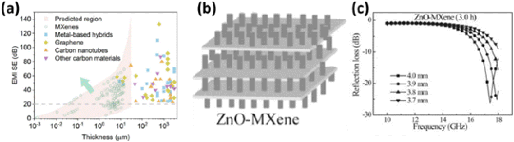 | ||
| Fig. 12 (a) Performance comparison of various MXenes with other materials for EMI shielding applications.202 (b) Schematic representation of the ZnO/Ti3C2Tx hybrids for improved EM absorption.204 (c) Reflection loss of ZnO/Ti3C2Tx nanocomposite at various frequencies.204 | ||
Combining different dimensional materials with MXenes is another effective tool for improving the EM wave absorption properties. The dielectric properties of MXenes could be tuned by incorporating interlayer spacers. Li et al. have combined the 2D Ti3C2Tx MXenes with 1D CNTs for designing a new kind of EM wave absorbing materials.203 The hybrid materials were grown using chemical vapor deposition technique. As compared to pristine Ti3C2Tx MXene, the nanocomposite showed higher absorption bandwidth due to more conductive paths and increased defects, confirming favorable polarization. Qian et al. have also developed MXenes-based nanocomposites for enhanced EM absorption.204 The hybrid was formed by combing Ti3C2 MXene with ZnO nanorods as shown in Fig. 12b. To form the hybrid ZnO was chosen as it possesses environmental stability, low cost, and multifunctional behavior. The composite showed promising absorption properties as shown in Fig. 12c. At a thickness of 4 mm, the maximum reflection loss was achieved −26.30 dB at 17.4 GHz. However, pristine Ti3C2Tx showed a higher reflection loss of −6.70 dB with the same thickness. Therefore, the EM absorption performance improved significantly upon forming the nanocomposite.
The MXenes are also fabricated using different etching times as it strongly affects the structures and EM properties of MXenes. Tong et al. have studied the effects of etching time on the morphology and dielectric properties of MXenes.205 Microwave shielding/absorbing properties changes with change in etching timings. Ti3C2Tx MXenes showed −42.5 dB of reflection loss and 13.8 GHz bandwidth at an optimum etching time of 24 hours. The enhanced absorption behavior of MXenes was ascribed to interfacial and dipole polarizations. Moreover, the EM properties of MXenes could also be modified with a rapid annealing technique. The heat treatment process controls the surface morphology, surface functional groups, and dielectric losses of MXenes.206
Moreover, the size of MXenes also plays a crucial role in determining its specific applications. For instance, nano-size MXenes are more suitable for biological fields.207 The size of MXenes primarily depends on the type of synthesizing technique, processing parameters, kind of etchant, and etching time. Generally, the conventional synthesizing techniques produce large-size MXenes having major safety concerns and poor therapeutic results in the biomedical field. Moreover, smaller size MXenes could easily penetrate into the circulatory system and be used for cancer treatment.208 In contrast, for high electrical conductivity applications, large-size MXenes with few defects are preferred.209 The larger size of MXenes could be obtained by using mild etchant and making contact among isolated flakes by removing interlayer spacing with intercalation. The larger surface area of MXenes facilitates a high value of capacitance and could potentially be used for energy storage applications. In addition, for advanced storage, 3D printing could be used for designing electrodes. High viscosity is desirable for developing extrusion printing. The shape and adhesion of printed structures are primarily dependent on the ink's viscoelastic properties. To improve the viscosity of MXenes for 3D printing applications, Yu et al. have mixed 1.67 g CNT into 0.7 g of NiCoP/Ti3C2 composite.210 The high viscous ink was used for designing printed electrodes for achieving a very high value of capacitance.
9. Conclusions and perspectives
This review comprehensively summarizes the state-of-art advancements of MXenes in various potential fields. MXenes possess several unique inherent characteristics making them suitable for a variety of applications. Different compositions and surface terminations of MXenes facilitate distinct features for developing novel electronic devices. In addition, MXenes could also be easily combined with other dimensional materials and form smart materials. The surface chemistry such as surface strain and defect engineering provide an extra edge for discovering futuristic electronic devices. MXenes possess large surface area, high conductivity, efficient photocarrier separation, and high signal to noise ratio confirming its ability for potential application.To exploit fullest potential of MXenes, many questions need to be answered to understand their inherent characteristics. Most of the newly discovered MXenes showed promising results, however, their underlying physics is still debated. More research needs to be done to explore their exciting physical phenomena. The discovery of new MAX phases is essential for transforming them into new kinds of MXenes families. Moreover, for newly discovered MXenes family members, experimental investigations are required to support the theoretical predictions. For developing MXenes based future technologies, environmentally friendly scale up synthesis techniques are also required. MXenes without surface termination might evolve some impressive chemistry and physics. However, they have been not synthesized yet. Some ultrahigh vacuum-based techniques could be utilized for their development.
Over the last decade, numerous 2D material families have matured significantly to meet the commercial objectives. However, MXenes still remain at their nascent stage and many formidable challenges need to be addressed to make them suitable for practical applications. Some of the MXenes suffer from poor stability problems, leading to unstable performance over long periods of time. For example, Ti3C2Tx is widely used for photocatalytic applications, but its instability leads to an unsteady performance. Efforts are made to improve the stability through surface functionalization techniques. In addition, tuning the porosity and morphology of MXenes increases the surface area and active sites, which strongly influences the storage capacities of the devices. Nevertheless, controlling the porosity and morphology of 2D MXene films still requires intensive research. Moreover, unlike graphene and other 2D materials, synthesizing a wafer-scale monolayer of MXenes still remains a key challenge for their commercial applications. As a future perspective, new MXenes with distinct physical and chemical properties are expected to be discovered and pave the way for next-generation energy storage, energy conversion, and flexible electronic devices.
Data availability statement
Data is available on request.Conflicts of interest
There are no conflicts to declare.References
- D. Chen, L. Tang and J. Li, Chem. Soc. Rev., 2010, 39, 3157 RSC.
- K. S. Novoselov, D. V. Andreeva, W. Ren and G. Shan, Front. Phys., 2019, 14, 13301 CrossRef.
- W. Li, X. Qian and J. Li, Nat. Rev. Mater., 2021, 6, 829–846 CrossRef CAS.
- Y. Li, K.-A. N. Duerloo, K. Wauson and E. J. Reed, Nat. Commun., 2016, 7, 10671 CrossRef CAS PubMed.
- T. Tan, X. Jiang, C. Wang, B. Yao and H. Zhang, Adv. Sci., 2020, 7, 2000058 CrossRef CAS PubMed.
- M. Dragoman, A. Dinescu and D. Dragoman, Phys. Status Solidi, 2019, 216, 1800724 CrossRef.
- H. Zhang, J. Wang, T. Hasan and Q. Bao, Opt. Commun., 2018, 406, 1–2 CrossRef CAS.
- R. Kumar, N. Goel and M. Kumar, ACS Sens., 2017, 2, 1744–1752 CrossRef CAS PubMed.
- W. Choi, N. Choudhary, G. H. Han, J. Park, D. Akinwande and Y. H. Lee, Mater. Today, 2017, 20, 116–130 CrossRef CAS.
- N. Goel and M. Kumar, J. Mater. Chem. C, 2021, 9, 1537–1549 RSC.
- E. Samuel Reich, Nature, 2014, 506, 19 CrossRef CAS PubMed.
- D. Jose and A. Datta, Acc. Chem. Res., 2014, 47, 593–602 CrossRef CAS PubMed.
- Z. Ni, Q. Liu, K. Tang, J. Zheng, J. Zhou, R. Qin, Z. Gao, D. Yu and J. Lu, Nano Lett., 2012, 12, 113–118 CrossRef CAS PubMed.
- M. Naguib, V. N. Mochalin, M. W. Barsoum and Y. Gogotsi, Adv. Mater., 2014, 26, 992–1005 CrossRef CAS PubMed.
- N. Li, Y. Jiang, Y. Xiao, B. Meng, C. Xing, H. Zhang and Z. Peng, Nanoscale, 2019, 11, 21522–21531 RSC.
- Y. Chae, S. J. Kim, S.-Y. Cho, J. Choi, K. Maleski, B.-J. Lee, H.-T. Jung, Y. Gogotsi, Y. Lee and C. W. Ahn, Nanoscale, 2019, 11, 8387–8393 RSC.
- S. J. Kim, H.-J. Koh, C. E. Ren, O. Kwon, K. Maleski, S.-Y. Cho, B. Anasori, C.-K. Kim, Y.-K. Choi, J. Kim, Y. Gogotsi and H.-T. Jung, ACS Nano, 2018, 12, 986–993 CrossRef CAS PubMed.
- J. Orangi, H. Tetik, P. Parandoush, E. Kayali, D. Lin and M. Beidaghi, Mater. Today Adv., 2021, 9, 100135 CrossRef CAS.
- J. Björk and J. Rosen, Chem. Mater., 2021, 33, 9108–9118 CrossRef.
- R. Bhardwaj and A. Hazra, J. Mater. Chem. C, 2021, 9, 15735–15754 RSC.
- M. Naguib, M. Kurtoglu, V. Presser, J. Lu, J. Niu, M. Heon, L. Hultman, Y. Gogotsi and M. W. Barsoum, Adv. Mater., 2011, 23, 4248–4253 CrossRef CAS PubMed.
- J. Pang, R. G. Mendes, A. Bachmatiuk, L. Zhao, H. Q. Ta, T. Gemming, H. Liu, Z. Liu and M. H. Rummeli, Chem. Soc. Rev., 2019, 48, 72–133 RSC.
- C. Ma, M. Ma, C. Si, X. Ji and P. Wan, Adv. Funct. Mater., 2021, 31, 2009524 CrossRef CAS.
- Z. Liu and H. N. Alshareef, Adv. Electron. Mater., 2021, 7, 2100295 CrossRef CAS.
- H. Huang, C. Dong, W. Feng, Y. Wang, B. Huang and Y. Chen, Adv. Drug Delivery Rev., 2022, 184, 114178 CrossRef CAS PubMed.
- D. H. Ho, Y. Y. Choi, S. B. Jo, J. Myoung and J. H. Cho, Adv. Mater., 2021, 33, 2005846 CrossRef CAS PubMed.
- L. Verger, V. Natu, M. Carey and M. W. Barsoum, Trends Chem., 2019, 1, 656–669 CrossRef CAS.
- G. Gao, G. Ding, J. Li, K. Yao, M. Wu and M. Qian, Nanoscale, 2016, 8, 8986–8994 RSC.
- C. Si, J. Zhou and Z. Sun, ACS Appl. Mater. Interfaces, 2015, 7, 17510–17515 CrossRef CAS PubMed.
- M. Khazaei, V. Wang, C. Sevik, A. Ranjbar, M. Arai and S. Yunoki, Phys. Rev. Mater., 2018, 2, 074002 CrossRef CAS.
- B. Anasori, Y. Xie, M. Beidaghi, J. Lu, B. C. Hosler, L. Hultman, P. R. C. Kent, Y. Gogotsi and M. W. Barsoum, ACS Nano, 2015, 9, 9507–9516 CrossRef CAS PubMed.
- H. Kumar, N. C. Frey, L. Dong, B. Anasori, Y. Gogotsi and V. B. Shenoy, ACS Nano, 2017, 11, 7648–7655 CrossRef CAS PubMed.
- R. A. de Groot, F. M. Mueller, P. G. van Engen and K. H. J. Buschow, Phys. Rev. Lett., 1983, 50, 2024–2027 CrossRef CAS.
- A. Champagne, L. Shi, T. Ouisse, B. Hackens and J.-C. Charlier, Phys. Rev. B, 2018, 97, 115439 CrossRef CAS.
- M. Khazaei, A. Mishra, N. S. Venkataramanan, A. K. Singh and S. Yunoki, Curr. Opin. Solid State Mater. Sci., 2019, 23, 164–178 CrossRef CAS.
- T. Hu, J. Wang, H. Zhang, Z. Li, M. Hu and X. Wang, Phys. Chem. Chem. Phys., 2015, 17, 9997–10003 RSC.
- M. Kurtoglu, M. Naguib, Y. Gogotsi and M. W. Barsoum, MRS Commun., 2012, 2, 133–137 CrossRef CAS.
- J.-C. Lei, X. Zhang and Z. Zhou, Front. Phys., 2015, 10, 276–286 CrossRef.
- M. Xing, B. Qiu, X. Li and J. Zhang, TiO2/Graphene Composites with Excellent Performance in Photocatalysis, 2016 Search PubMed.
- B. A. Pinaud, J. D. Benck, L. C. Seitz, A. J. Forman, Z. Chen, T. G. Deutsch, B. D. James, K. N. Baum, G. N. Baum, S. Ardo, H. Wang, E. Miller and T. F. Jaramillo, Energy Environ. Sci., 2013, 6, 1983–2002 RSC.
- M. Z. Rahman, J. Ran, Y. Tang, M. Jaroniec and S. Z. Qiao, J. Mater. Chem. A, 2016, 4, 2445–2452 RSC.
- A. A. Ismail and D. W. Bahnemann, Sol. Energy Mater. Sol. Cells, 2014, 128, 85–101 CrossRef CAS.
- R. Kuriki, K. Sekizawa, O. Ishitani and K. Maeda, Angew. Chem., Int. Ed., 2015, 54, 2406–2409 CrossRef CAS PubMed.
- J. L. White, M. F. Baruch, J. E. Pander, Y. Hu, I. C. Fortmeyer, J. E. Park, T. Zhang, K. Liao, J. Gu, Y. Yan, T. W. Shaw, E. Abelev and A. B. Bocarsly, Chem. Rev., 2015, 115, 12888–12935 CrossRef CAS PubMed.
- S. Pal, S. Maiti, U. N. Maiti and K. K. Chattopadhyay, CrystEngComm, 2015, 17, 1464–1476 RSC.
- R. C. Pawar, V. Khare and C. S. Lee, Dalton Trans., 2014, 43, 12514–12527 RSC.
- H. Y. Jing, T. Wen, C. M. Fan, G. Q. Gao, S. L. Zhong and A. W. Xu, J. Mater. Chem. A, 2014, 2, 14563–14570 RSC.
- S. E. Mousavinia, S. Hajati, M. Ghaedi and K. Dashtian, Phys. Chem. Chem. Phys., 2016, 18, 11278–11287, 10.1039/C6CP00910G.
- P. Kumar, A. Kumar, C. Joshi, R. Boukherroub and S. L. Jain, Advanced 2D Materials, 2016, 355 DOI:10.1002/9781119242635.ch9.
- S. Deng, Y. Zhong, Y. Zeng, Y. Wang, Z. Yao, F. Yang, S. Lin, X. Wang, X. Lu, X. Xia and J. Tu, Adv. Mater., 2017, 29, 1–8 Search PubMed.
- S. Deng, Y. Zhong, Y. Zeng, Y. Wang, X. Wang, X. Lu, X. Xia and J. Tu, Adv. Sci., 2018, 5, 1–8 Search PubMed.
- C. Peng, X. Yang, Y. Li, H. Yu, H. Wang and F. Peng, ACS Appl. Mater. Interfaces, 2016, 8, 6051–6060 CrossRef CAS PubMed.
- I. Persson, A. el Ghazaly, Q. Tao, J. Halim, S. Kota, V. Darakchieva, J. Palisaitis, M. W. Barsoum, J. Rosen and P. O. Å. Persson, Small, 2018, 14, 1–7 Search PubMed.
- Y. Dong, S. S. K. Mallineni, K. Maleski, H. Behlow, V. N. Mochalin, A. M. Rao, Y. Gogotsi and R. Podila, Nano Energy, 2018, 44, 103–110 CrossRef CAS.
- A. D. Handoko, K. D. Fredrickson, B. Anasori, K. W. Convey, L. R. Johnson, Y. Gogotsi, A. Vojvodic and Z. W. Seh, ACS Appl. Energy Mater., 2018, 1, 173–180 CrossRef CAS.
- K. Nagaveni, G. Sivalingam, M. S. Hegde and G. Madras, Environ. Sci. Technol., 2004, 38, 1600–1604 CrossRef CAS PubMed.
- H. Zhang, R. Zong, J. Zhao and Y. Zhu, Environ. Sci. Technol., 2008, 42, 3803–3807 CrossRef CAS PubMed.
- Z. Guo, J. Zhou, L. Zhu and Z. Sun, J. Mater. Chem. A, 2016, 4, 11446–11452 RSC.
- M. Mariano, O. Mashtalir, F. Q. Antonio, W. H. Ryu, B. Deng, F. Xia, Y. Gogotsi and A. D. Taylor, Nanoscale, 2016, 8, 16371–16378 RSC.
- X. Li, Z. Lv and H. Zhu, Adv. Mater., 2015, 27, 6549–6574 CrossRef CAS PubMed.
- X. Li and H. Zhu, Phys. Today, 2016, 69, 46–51 CrossRef CAS.
- Z. Kang, Y. Ma, X. Tan, M. Zhu, Z. Zheng, N. Liu, L. Li, Z. Zou, X. Jiang, T. Zhai and Y. Gao, Adv. Electron. Mater., 2017, 3, 1–7 Search PubMed.
- G. Möbus, R. C. Doole and B. J. Inkson, Ultramicroscopy, 2003, 96, 433–451 CrossRef.
- Z. Guo, N. Miao, J. Zhou, B. Sa and Z. Sun, J. Mater. Chem. C, 2017, 5, 978–984 RSC.
- J. Zhou and P. Jena, J. Phys. Chem. Lett., 2017, 8, 5764–5770 CrossRef CAS PubMed.
- Q. Yang, S. Zhang, C. Tan, H. Ye, X. Ming, S. Ingebrandt and X. Chen, J. Mater. Chem. C, 2017, 5, 9412–9420 RSC.
- G. W. Jones, D. A. Bahamon, A. H. Castro Neto and V. M. Pereira, Nano Lett., 2017, 17, 5304–5313 CrossRef CAS PubMed.
- M. Kang, B. Kim, S. H. Ryu, S. W. Jung, J. Kim, L. Moreschini, C. Jozwiak, E. Rotenberg, A. Bostwick and K. S. Kim, Nano Lett., 2017, 17, 1610–1615 CrossRef CAS PubMed.
- Z. Wang, L. Zhao, K. F. Mak and J. Shan, Nano Lett., 2017, 17, 740–746 CrossRef CAS PubMed.
- C. Niu, P. M. Buhl, G. Bihlmayer, D. Wortmann, Y. Dai, S. Blügel and Y. Mokrousov, Phys. Rev. B, 2017, 95, 3–7 Search PubMed.
- P. P. Patel, M. K. Datta, O. I. Velikokhatnyi, P. Jampani, D. Hong, J. A. Poston, A. Manivannan and P. N. Kumta, J. Mater. Chem. A, 2015, 3, 14015–14032 RSC.
- T.-Y. Chen, Y.-H. Chang, C.-L. Hsu, K.-H. Wei, C.-Y. Chiang and L.-J. Li, Int. J. Hydrogen Energy, 2013, 38, 12302–12309 CrossRef CAS.
- H. Pan, Sci. Rep., 2016, 6, 32531 CrossRef CAS PubMed.
- K. Keum, J. W. Kim, S. Y. Hong, J. G. Son, S. S. Lee and J. S. Ha, Adv. Mater., 2020, 32, 1–34 CrossRef PubMed.
- R. Khan and S. Andreescu, Sensors, 2020, 20, 1–19 Search PubMed.
- J. Yoon, H. Y. Cho, M. Shin, H. K. Choi, T. Lee and J. W. Choi, J. Mater. Chem. B, 2020, 8, 7303–7318 RSC.
- B. Peng, F. Zhao, J. Ping and Y. Ying, Small, 2020, 16, 1–24 Search PubMed.
- C. Wang, K. Xia, H. Wang, X. Liang, Z. Yin and Y. Zhang, Adv. Mater., 2019, 31, 1–37 Search PubMed.
- F. Shahzad, A. Iqbal, H. Kim and C. M. Koo, Adv. Mater., 2020, 32, 1–23 CrossRef PubMed.
- N. Afsarimanesh, A. Nag, S. Sarkar, G. S. Sabet, T. Han and S. C. Mukhopadhyay, Sens. Actuators, A, 2020, 315, 112355 CrossRef CAS.
- M. Amjadi, K. U. Kyung, I. Park and M. Sitti, Adv. Funct. Mater., 2016, 26, 1678–1698 CrossRef CAS.
- Y. Jiang, Z. Liu, C. Wang and X. Chen, Acc. Chem. Res., 2019, 52, 82–90 CrossRef CAS PubMed.
- Y. Zang, F. Zhang, C. A. Di and D. Zhu, Mater. Horiz., 2015, 2, 140–156 RSC.
- Y. Cai, J. Shen, G. Ge, Y. Zhang, W. Jin, W. Huang, J. Shao, J. Yang and X. Dong, ACS Nano, 2018, 12, 56–62 CrossRef CAS PubMed.
- Y. Yang, Z. Cao, P. He, L. Shi, G. Ding, R. Wang and J. Sun, Nano Energy, 2019, 66, 104134, DOI:10.1016/j.nanoen.2019.104134.
- Y. Yang, L. Shi, Z. Cao, R. Wang and J. Sun, Adv. Funct. Mater., 2019, 29, 1–10 Search PubMed.
- Y. Yang, Z. Cao, P. He, L. Shi, G. Ding, R. Wang and J. Sun, Nano Energy, 2019, 66, 104134 CrossRef CAS.
- M. Chen, X. Hu, K. Li, J. Sun, Z. Liu, B. An, X. Zhou and Z. Liu, Carbon, 2020, 164, 111–120 CrossRef CAS.
- T. Li, L. Chen, X. Yang, X. Chen, Z. Zhang, T. Zhao, X. Li and J. Zhang, J. Mater. Chem. C, 2019, 7, 1022–1027 RSC.
- C. Ma, Q. Yuan, H. Du, M. G. Ma, C. Si and P. Wan, ACS Appl. Mater. Interfaces, 2020, 12, 34226–34234 CrossRef CAS PubMed.
- Y. Guo, M. Zhong, Z. Fang, P. Wan and G. Yu, Nano Lett., 2019, 19, 1143–1150 CrossRef CAS PubMed.
- Y. Yue, N. Liu, W. Liu, M. Li, Y. Ma, C. Luo, S. Wang, J. Rao, X. Hu, J. Su, Z. Zhang, Q. Huang and Y. Gao, Nano Energy, 2018, 50, 79–87 CrossRef CAS.
- Z. Chen, Y. Hu, H. Zhuo, L. Liu, S. Jing, L. Zhong, X. Peng and R. C. Sun, Chem. Mater., 2019, 31, 3301–3312 CrossRef CAS.
- H. Zhuo, Y. Hu, Z. Chen, X. Peng, L. Liu, Q. Luo, J. Yi, C. Liu and L. Zhong, J. Mater. Chem. A, 2019, 7, 8092–8100 RSC.
- S. J. Wang, D. Sen Li and L. Jiang, Adv. Mater. Interfaces, 2019, 6, 1–9 CAS.
- Y. Cheng, Y. Ma, L. Li, M. Zhu, Y. Yue, W. Liu, L. Wang, S. Jia, C. Li, T. Qi, J. Wang and Y. Gao, ACS Nano, 2020, 14, 2145–2155 CrossRef CAS PubMed.
- H. Kim, G. Yoon, K. Lim and K. Kang, Chem. Commun., 2016, 52, 12618–12621 RSC.
- Y. Zhao and A. Manthiram, Chem. Commun., 2015, 51, 13205–13208 RSC.
- Z. Zhu, F. Cheng, Z. Hu, Z. Niu and J. Chen, J. Power Sources, 2015, 293, 626–634 CrossRef CAS.
- R. Zhang, F. Mizuno and C. Ling, Chem. Commun., 2015, 51, 1108–1111 RSC.
- P. Sood, K. C. Kim and S. S. Jang, J. Energy Chem., 2018, 27, 528–534 CrossRef.
- P. Bairi, R. G. Shrestha, J. P. Hill, T. Nishimura, K. Ariga and L. K. Shrestha, J. Mater. Chem. A, 2016, 4, 13899–13906 RSC.
- Y. Fu, Y. S. Su and A. Manthiram, Angew. Chem., Int. Ed., 2013, 52, 6930–6935 CrossRef CAS PubMed.
- D. Kong, X. Li, Y. Zhang, X. Hai, B. Wang, X. Qiu, Q. Song, Q. Yang and L. Zhi, Energy Environ. Sci., 2016, 9, 2666 RSC.
- M. Xie, X. Sun, H. Sun, T. Porcelli, S. M. George, Y. Zhou and J. Lian, J. Mater. Chem. A, 2016, 4, 537–544 RSC.
- T. Kowase, K. Hori, K. Hasegawa, T. Momma and S. Noda, J. Power Sources, 2017, 363, 450–459 CrossRef CAS.
- M. Yu, J. Ma, H. Song, A. Wang, F. Tian, Y. Wang, H. Qiu and R. Wang, Energy Environ. Sci., 2016, 9, 1495–1503 RSC.
- D. Li, L. Zhang, H. Chen, J. Wang, L.-X. Ding, S. Wang, P. J. Ashman and H. Wang, J. Mater. Chem. A, 2016, 4, 8630–8635 RSC.
- V. Ivaništšev, T. Méndez-Morales, R. M. Lynden-Bell, O. Cabeza, L. J. Gallego, L. M. Varela and M. V. Fedorov, Phys. Chem. Chem. Phys., 2016, 18, 1302–1310 RSC.
- K.-Y. Zhou, G.-Y. Chen, J.-A. Liu, Z.-P. Zhang, P. Sun, W.-Z. Zhang, F. Niu, W.-X. Zhang and J.-C. Liang, RSC Adv., 2016, 6, 90069–90075 RSC.
- X. Wang, Q. Weng, Y. Yang, Y. Bando and D. Golberg, Chem. Soc. Rev., 2016, 45, 4042–4073 RSC.
- Y.-P. Gao, X. Wu, K.-J. Huang, L.-L. Xing, Y.-Y. Zhang and L. Liu, CrystEngComm, 2017, 19, 404–418 RSC.
- S. K. Balasingam, J. S. Lee and Y. Jun, Dalton Trans., 2016, 45, 9646–9653 RSC.
- A. Eftekhari, J. Mater. Chem. A, 2017, 5, 18299–18325 RSC.
- Z. Sofer, D. Bouša, J. Luxa, V. Mazanek and M. Pumera, Chem. Commun., 2016, 52, 1563–1566 RSC.
- J. Zhao, Y. Yang, R. S. Katiyar and Z. Chen, J. Mater. Chem. A, 2016, 4, 6124–6130 RSC.
- Q. Xia, W. Li, Z. Miao, S. Chou and H. Liu, Nano Res., 2017, 10, 4055–4081 CrossRef CAS.
- M. Qiu, Z. T. Sun, D. K. Sang, X. G. Han, H. Zhang and C. M. Niu, Nanoscale, 2017, 9, 13384–13403 RSC.
- S. Sarkar, P. Howli, B. Das, N. S. Das, M. Samanta, G. C. Das and K. K. Chattopadhyay, ACS Appl. Mater. Interfaces, 2017, 9, 22652–22664 CrossRef CAS PubMed.
- B. K. Deka, A. Hazarika, J. Kim, Y.-B. Park and H. W. Park, Int. J. Energy Res., 2017, 41, 1397–1411 CrossRef.
- S. Bag and C. R. Raj, J. Mater. Chem. A, 2016, 4, 587–595 RSC.
- M. Jana, J. S. Kumar, P. Khanra, P. Samanta, H. Koo, N. C. Murmu and T. Kuila, J. Power Sources, 2016, 303, 222–233 CrossRef CAS.
- Y. Li, Z. Chen, J. Zhang and Q. Xu, RSC Adv., 2016, 6, 9180–9185 RSC.
- T. M. Masikhwa, M. J. Madito, D. Y. Momodu, J. K. Dangbegnon, O. Guellati, A. Harat, M. Guerioune, F. Barzegar and N. Manyala, RSC Adv., 2016, 6, 46723–46732 RSC.
- A. Kafy, A. Akther, L. Zhai, H. C. Kim and J. Kim, Synth. Met., 2017, 223, 94–100 CrossRef CAS.
- C. Eames and M. S. Islam, J. Am. Chem. Soc., 2014, 136, 16270–16276 CrossRef CAS PubMed.
- Y. Xie, M. Naguib, V. N. Mochalin, M. W. Barsoum, Y. Gogotsi, X. Yu, K.-W. Nam, X.-Q. Yang, A. I. Kolesnikov and P. R. C. Kent, J. Am. Chem. Soc., 2014, 136, 6385–6394 CrossRef CAS PubMed.
- C. E. Ren, M. Zhao, T. Makaryan, J. Halim, M. Boota, S. Kota, B. Anasori, M. W. Barsoum and Y. Gogotsi, ChemElectroChem, 2016, 3, 689–693 CrossRef CAS.
- Y. Xie, Y. Dall’Agnese, M. Naguib, Y. Gogotsi, M. W. Barsoum, H. L. Zhuang and P. RC Kent, ACS nano, 2014, 8, 9606–9615 CrossRef CAS PubMed.
- M. Cai, R. A. Outlaw, R. A. Quinlan, D. Premathilake, S. M. Butler and J. R. Miller, ACS Nano, 2014, 8, 5873–5882 CrossRef CAS PubMed.
- Y. Lu, F. Zhang, T. Zhang, K. Leng, L. Zhang, X. Yang, Y. Ma, Y. Huang, M. Zhang and Y. Chen, Carbon, 2013, 63, 508–516 CrossRef CAS.
- L. Zhang, X. Yang, F. Zhang, G. Long, T. Zhang, K. Leng, Y. Zhang, Y. Huang, Y. Ma, M. Zhang and Y. Chen, J. Am. Chem. Soc., 2013, 135, 5921–5929 CrossRef CAS PubMed.
- Y. Wang, Z. Shi, Y. Huang, Y. Ma, C. Wang, M. Chen and Y. Chen, J. Phys. Chem. C, 2009, 113, 13103–13107 CrossRef CAS.
- L. Zhang, F. Zhang, X. Yang, K. Leng, Y. Huang and Y. Chen, Small, 2013, 9, 1342–1347 CrossRef CAS PubMed.
- W. Xiong, Y. Gao, X. Wu, X. Hu, D. Lan, Y. Chen, X. Pu, Y. Zeng, J. Su and Z. Zhu, ACS Appl. Mater. Interfaces, 2014, 6, 19416–19423 CrossRef CAS PubMed.
- Z. Jian, V. Raju, Z. Li, Z. Xing, Y.-S. Hu and X. Ji, Adv. Funct. Mater., 2015, 25, 5778–5785 CrossRef CAS.
- B. P. Bastakoti, H.-S. Huang, L.-C. Chen, K. C.-W. Wu and Y. Yamauchi, Chem. Commun., 2012, 48, 9150 RSC.
- Y. Wang, S. F. Yu, C. Y. Sun, T. J. Zhu and H. Y. Yang, J. Mater. Chem., 2012, 22, 17584 RSC.
- H. Chen, J. Jiang, L. Zhang, H. Wan, T. Qi and D. Xia, Nanoscale, 2013, 5, 8879 RSC.
- J. Li, M. Yang, J. Wei and Z. Zhou, Nanoscale, 2012, 4, 4498 RSC.
- M. Yang, J. X. Li, H. H. Li, L. W. Su, J. P. Wei and Z. Zhou, Phys. Chem. Chem. Phys., 2012, 14, 11048 RSC.
- Z.-S. Wu, W. Ren, D.-W. Wang, F. Li, B. Liu and H.-M. Cheng, ACS Nano, 2010, 4, 5835–5842 CrossRef CAS PubMed.
- Y. Huang, J. Liang and Y. Chen, Small, 2012, 8, 1805–1834 CrossRef CAS PubMed.
- Y. Shao, M. F. El-Kady, J. Sun, Y. Li, Q. Zhang, M. Zhu, H. Wang, B. Dunn and R. B. Kaner, Chem. Rev., 2018, 118, 9233–9280 CrossRef CAS PubMed.
- C. J. Zhang, M. P. Kremer, A. Seral-Ascaso, S.-H. Park, N. McEvoy, B. Anasori, Y. Gogotsi and V. Nicolosi, Adv. Funct. Mater., 2018, 28, 1705506 CrossRef.
- C. Couly, M. Alhabeb, K. L. Van Aken, N. Kurra, L. Gomes, A. M. Navarro-Suárez, B. Anasori, H. N. Alshareef and Y. Gogotsi, Adv. Electron. Mater., 2018, 4, 1700339 CrossRef.
- Y. Tian, C. Yang, W. Que, X. Liu, X. Yin and L. B. Kong, J. Power Sources, 2017, 359, 332–339 CrossRef CAS.
- M. R. Lukatskaya, S. Kota, Z. Lin, M.-Q. Zhao, N. Shpigel, M. D. Levi, J. Halim, P.-L. Taberna, M. W. Barsoum, P. Simon and Y. Gogotsi, Nat. Energy, 2017, 2, 17105 CrossRef CAS.
- Z.-S. Wu, D.-W. Wang, W. Ren, J. Zhao, G. Zhou, F. Li and H.-M. Cheng, Adv. Funct. Mater., 2010, 20, 3595–3602 CrossRef CAS.
- S. Cho, J. Kim, Y. Jo, A. T. A. Ahmed, H. S. Chavan, H. Woo, A. I. Inamdar, J. L. Gunjakar, S. M. Pawar, Y. Park, H. Kim and H. Im, J. Alloys Compd., 2017, 725, 108–114 CrossRef CAS.
- I. Ryu, M. Yang, H. Kwon, H. K. Park, Y. R. Do, S. B. Lee and S. Yim, Langmuir, 2014, 30, 1704–1709 CrossRef CAS PubMed.
- C.-C. Hu, K.-H. Chang, M.-C. Lin and Y.-T. Wu, Nano Lett., 2006, 6, 2690–2695 CrossRef CAS PubMed.
- H. Ma, D. Kong, Y. Xu, X. Xie, Y. Tao, Z. Xiao, W. Lv, H. D. Jang, J. Huang and Q. Yang, Small, 2017, 13, 1701026 CrossRef PubMed.
- L. L. Zhang and X. S. Zhao, Chem. Soc. Rev., 2009, 38, 2520 RSC.
- G. K. Ramesha and S. Sampath, in Graphene, Wiley, 2012, pp. 269–301 Search PubMed.
- Y. Sun, Q. Wu, Y. Xu, H. Bai, C. Li and G. Shi, J. Mater. Chem., 2011, 21, 7154 RSC.
- Z.-S. Wu, K. Parvez, S. Li, S. Yang, Z. Liu, S. Liu, X. Feng and K. Müllen, Adv. Mater., 2015, 27, 4054–4061 CrossRef CAS PubMed.
- Z. Wang, P. Tammela, M. Strømme and L. Nyholm, Nanoscale, 2015, 7, 3418–3423 RSC.
- C. Liu, Z. Yu, D. Neff, A. Zhamu and B. Z. Jang, Nano Lett., 2010, 10, 4863–4868 CrossRef CAS PubMed.
- Q. Cheng, J. Tang, J. Ma, H. Zhang, N. Shinya and L.-C. Qin, Phys. Chem. Chem. Phys., 2011, 13, 17615 RSC.
- B. G. Choi, M. Yang, W. H. Hong, J. W. Choi and Y. S. Huh, ACS Nano, 2012, 6, 4020–4028 CrossRef CAS PubMed.
- A. Yu, I. Roes, A. Davies and Z. Chen, Appl. Phys. Lett., 2010, 96, 253105 CrossRef.
- L. L. Zhang, X. Zhao, M. D. Stoller, Y. Zhu, H. Ji, S. Murali, Y. Wu, S. Perales, B. Clevenger and R. S. Ruoff, Nano Lett., 2012, 12, 1806–1812 CrossRef CAS PubMed.
- X. Zhao, B. M. Sánchez, P. J. Dobson and P. S. Grant, Nanoscale, 2011, 3, 839 RSC.
- V. Sudha and M. V. Sangaranarayanan, J. Phys. Chem. B, 2002, 106, 2699–2707 CrossRef CAS.
- L. Kong, C. Zhang, S. Zhang, J. Wang, R. Cai, C. Lv, W. Qiao, L. Ling and D. Long, J. Mater. Chem. A, 2014, 2, 17962–17970 RSC.
- F. Schedin, A. K. Geim, S. V. Morozov, E. W. Hill, P. Blake, M. I. Katsnelson and K. S. Novoselov, Nat. Mater., 2007, 6, 652–655 CrossRef CAS PubMed.
- Y. Zhang, Z. Zhou, J. Lan and P. Zhang, Appl. Surf. Sci., 2019, 469, 770–774 CrossRef CAS.
- C. E. Shuck, M. Han, K. Maleski, K. Hantanasirisakul, S. J. Kim, J. Choi, W. E. B. Reil and Y. Gogotsi, ACS Appl. Nano Mater., 2019, 2, 3368–3376 CrossRef CAS.
- E. Lee, A. VahidMohammadi, B. C. Prorok, Y. S. Yoon, M. Beidaghi and D.-J. Kim, ACS Appl. Mater. Interfaces, 2017, 9, 37184–37190 CrossRef CAS PubMed.
- S. J. Kim, J. Choi, K. Maleski, K. Hantanasirisakul, H.-T. Jung, Y. Gogotsi and C. W. Ahn, ACS Appl. Mater. Interfaces, 2019, 11, 32320–32327 CrossRef CAS PubMed.
- R. Li, Y. Fan, Z. Ma, D. Zhang, Y. Liu and J. Xu, Microchim. Acta, 2021, 188, 81 CrossRef CAS PubMed.
- L. Wang, M. Tian, Y. Zhang, F. Sun, X. Qi, Y. Liu and L. Qu, J. Mater. Sci., 2020, 55, 6187–6194 CrossRef CAS.
- X. Zhao, L.-Y. Wang, C.-Y. Tang, X.-J. Zha, Y. Liu, B.-H. Su, K. Ke, R.-Y. Bao, M.-B. Yang and W. Yang, ACS Nano, 2020, 14, 8793–8805 CrossRef CAS PubMed.
- K. Yang, K. Zhu, Y. Wang, Z. Qian, Y. Zhang, Z. Yang, Z. Wang, L. Wu, S. Zong and Y. Cui, ACS Nano, 2021, 15, 12996–13006 CrossRef CAS PubMed.
- M. Wu, M. He, Q. Hu, Q. Wu, G. Sun, L. Xie, Z. Zhang, Z. Zhu and A. Zhou, ACS Sens., 2019, 4, 2763–2770 CrossRef CAS PubMed.
- Y.-U. Haq, R. Ullah, S. Mazhar, R. Khattak, A. A. Qarni, Z.-U. Haq and S. Amin, J. Sci.: Adv. Mater. Devices, 2022, 7, 100390 CAS.
- E. S. Muckley, M. Naguib and I. N. Ivanov, Nanoscale, 2018, 10, 21689–21695 RSC.
- J. Wang, R. Xu, Y. Xia and S. Komarneni, Ceram. Int., 2021, 47, 34437–34442 CrossRef CAS.
- W.-N. Zhao, N. Yun, Z.-H. Dai and Y.-F. Li, RSC Adv., 2020, 10, 1261–1270 RSC.
- E. Lee, A. VahidMohammadi, Y. S. Yoon, M. Beidaghi and D.-J. Kim, ACS Sens., 2019, 4, 1603–1611 CrossRef CAS PubMed.
- W. Guo, S. G. Surya, V. Babar, F. Ming, S. Sharma, H. N. Alshareef, U. Schwingenschlögl and K. N. Salama, ACS Appl. Mater. Interfaces, 2020, 12, 57218–57227 CrossRef CAS PubMed.
- S.-Y. Cho, J. Y. Kim, O. Kwon, J. Kim and H.-T. Jung, J. Mater. Chem. A, 2018, 6, 23408–23416 RSC.
- Y. Tang, Y. Xu, J. Yang, Y. Song, F. Yin and W. Yuan, Sens. Actuators, B, 2021, 346, 130500 CrossRef CAS.
- J. Choi, Y. Kim, S. Cho, K. Park, H. Kang, S. J. Kim and H. Jung, Adv. Funct. Mater., 2020, 30, 2003998 CrossRef CAS.
- T. He, W. Liu, T. Lv, M. Ma, Z. Liu, A. Vasiliev and X. Li, Sens. Actuators, B, 2021, 329, 129275 CrossRef CAS.
- J. Wang, Y. Yang and Y. Xia, Sens. Actuators, B, 2022, 353, 131087 CrossRef CAS.
- C. Moore and J. V. Jokerst, Theranostics, 2019, 9, 1550–1571 CrossRef CAS PubMed.
- H. Lin, X. Wang, L. Yu, Y. Chen and J. Shi, Nano Lett., 2017, 17, 384–391 CrossRef CAS PubMed.
- C. Dai, Y. Chen, X. Jing, L. Xiang, D. Yang, H. Lin, Z. Liu, X. Han and R. Wu, ACS Nano, 2017, 11, 12696–12712 CrossRef CAS PubMed.
- C. Dai, H. Lin, G. Xu, Z. Liu, R. Wu and Y. Chen, Chem. Mater., 2017, 29, 8637–8652 CrossRef CAS.
- H. Lin, Y. Wang, S. Gao, Y. Chen and J. Shi, Adv. Mater., 2018, 30, 1703284 CrossRef PubMed.
- S. Zada, W. Dai, Z. Kai, H. Lu, X. Meng, Y. Zhang, Y. Cheng, F. Yan, P. Fu, X. Zhang and H. Dong, Angew. Chem., Int. Ed., 2020, 59, 6601–6606 CrossRef CAS PubMed.
- J. Shao, J. Zhang, C. Jiang, J. Lin and P. Huang, Chem. Eng. J., 2020, 400, 126009 CrossRef CAS.
- H. An, M. Mamuti, X. Wang, H. Yao, M. Wang, L. Zhao and L. Li, Exploration, 2021, 1, 20210153 CrossRef.
- T. Hu, X. Mei, Y. Wang, X. Weng, R. Liang and M. Wei, Sci. Bull., 2019, 64, 1707–1727 CrossRef CAS.
- X. Han, J. Huang, H. Lin, Z. Wang, P. Li and Y. Chen, Adv. Healthcare Mater., 2018, 7, 1701394 CrossRef PubMed.
- G. Liu, J. Zou, Q. Tang, X. Yang, Y. Zhang, Q. Zhang, W. Huang, P. Chen, J. Shao and X. Dong, ACS Appl. Mater. Interfaces, 2017, 9, 40077–40086 CrossRef CAS PubMed.
- A. Chaudhary, R. Kumar, S. R. Dhakate and S. Kumari, Composites, Part B, 2019, 158, 206–217 CrossRef CAS.
- S. Biswas, S. Dutta, S. S. Panja and S. Bose, ChemistrySelect, 2017, 2, 10840–10847 CrossRef CAS.
- X. Li, X. Yin, S. Liang, M. Li, L. Cheng and L. Zhang, Carbon, 2019, 146, 210–217 CrossRef CAS.
- M. Han, C. E. Shuck, R. Rakhmanov, D. Parchment, B. Anasori, C. M. Koo, G. Friedman and Y. Gogotsi, ACS Nano, 2020, 14, 5008–5016 CrossRef CAS PubMed.
- X. Li, X. Yin, M. Han, C. Song, H. Xu, Z. Hou, L. Zhang and L. Cheng, J. Mater. Chem. C, 2017, 5, 4068–4074 RSC.
- Y. Qian, H. Wei, J. Dong, Y. Du, X. Fang, W. Zheng, Y. Sun and Z. Jiang, Ceram. Int., 2017, 43, 10757–10762 CrossRef CAS.
- Y. Tong, M. He, Y. Zhou, X. Zhong, L. Fan, T. Huang, Q. Liao and Y. Wang, J. Mater. Sci.: Mater. Electron., 2018, 29, 8078–8088 CrossRef CAS.
- M. Han, X. Yin, H. Wu, Z. Hou, C. Song, X. Li, L. Zhang and L. Cheng, ACS Appl. Mater. Interfaces, 2016, 8, 21011–21019 CrossRef CAS PubMed.
- A. Zamhuri, G. P. Lim, N. L. Ma, K. S. Tee and C. F. Soon, Biomed. Eng. Online., 2021, 20, 33 CrossRef PubMed.
- B. Yang, Y. Chen and J. Shi, Chem, 2018, 4, 1284–1313 CAS.
- B. Anasori, M. R. Lukatskaya and Y. Gogotsi, Nat. Rev. Mater., 2017, 2, 16098 CrossRef CAS.
- L. Yu, W. Li, C. Wei, Q. Yang, Y. Shao and J. Sun, Nano-Micro Lett., 2020, 12, 143 CrossRef CAS PubMed.
| This journal is © The Royal Society of Chemistry 2022 |