
 Open Access Article
 This Open Access Article is licensed under a Creative Commons Attribution-Non Commercial 3.0 Unported Licence
Improving thermoelectric performance by constructing a SnTe/ZnO core–shell structure†
Song Lia,
Jingwen Zhang*ab,
Dawei Liua,
Yan Wanga and
Jiuxing Zhang *a
*a
aSchool of Materials Science and Engineering, Hefei University of Technology, Hefei 230009, China. E-mail: zjwhfut18205614071@163.com; zjiuxing@hfut.edu.cn
bSchool of Physics and Materials Engineering, Hefei Normal University, Hefei 230061, China
First published on 18th August 2022
Abstract
SnTe is becoming a new research focus as an intermediate temperature thermoelectric material for its environment-friendly property. Herein, the SnTe/ZnO core–shell structure prepared by a facile hydrothermal method is firstly constructed to enhance the thermoelectric performance. The characterization results demonstrate that ZnO nanosheets are coated on the surface of SnTe particles by in situ synthesis and converted into ZnO nano-dots by spark plasma sintering. The energy barriers built by the SnTe/ZnO core–shell structure improve the Seebeck coefficient effectively. Additionally, the increased density of interfaces induced by ZnO can effectively scatter low/medium frequency phonons, reducing the lattice thermal conductivity in the low/medium temperature region. Further, the point defects caused by Cu2Te-alloying strengthen the scattering of high frequency phonons. The lattice thermal conductivity reaches 0.48 W m−1 K−1, which is close to the amorphous limit of pristine SnTe. As a result, a peak ZT value of 0.94 is achieved at 823 K for SnTe(Cu2Te)0.06–1.5% ZnO, benefiting from the synergistic optimization of thermal and electrical properties. This provides a new idea for exploring an optimization strategy of thermoelectric performance.
1. Introduction
Due to the rising serious problem of environmental pollution and the depletion of non-renewable fossil fuels, the demand for developing and applying new clean energy is desired to be solved. Thermoelectric materials have a function of realizing direct conversion between heat and electricity without any moving parts, noise, or additional emissions.1–3 Thus, thermoelectric materials are receiving increasing attention for their potential application. The performance of thermoelectrical materials (TE) is expressed by the dimensionless figure of merit ZT = S2σT/κ, which is decided by three main physical parameters including the Seebeck coefficient, S, electrical conductivity, σ, and thermal conductivity, κ.4,5 So, we expect thermoelectrical materials to achieve a high ZT value with the characteristics of a high Seebeck coefficient, high electrical conductivity, and low thermal conductivity.6In the past few decades, intermediate temperature TE materials, such as Sb2Si2Te6,7 Bi2Si2Te6,8 GeTe,9 AgMnSbTe4,10 Mg3Sb2,11 and SnSe,12 have received widespread attention and undergone intensive research for their application prospects. For example, the well-investigated lead telluride (PbTe) based TE materials have obtained high ZT values, especially p-type PbTe.13–15 However, the toxicity of lead element limits their large-scale applications. SnTe-based TE materials have attracted much interest for their lead-free and environment-friendly characteristics.2 Moreover, SnTe has a similar rock salt crystal structure and electronic band structure with PbTe.16,17 Nevertheless, some reasons seriously limit the TE performance of the pristine SnTe: the intrinsic high hole concentration,18 a small band gap as well as a larger energy separation between the light and heavy valence bands,19 and the high lattice thermal conductivity.20
At present, there is much research on SnTe to optimize the TE performance. The formation of SnTe solid solution with mono-tellurides, such as MgTe,21 HgTe,22 CdTe,6,23 MnTe,24,25 CaTe26 can effectively enlarge the band gap to postpone the temperature at which the bipolar effect appears and reduce the separation between light and heavy valence band to realize valence band convergence, which is an effective way to optimize the Seebeck coefficient (S) and eventually the power factor (S2σ). Moreover, Zhang et al. proved that indium alloying can induce resonant state near the valence band of SnTe,27 which can improve the density of states (DOS) near Fermi level EF of SnTe and dramatically improve the S, especially at room temperature, realizing the power factor PF of ∼20.3 μW cm−1 K−2 and ZT value of ∼1.1 at 873 K in In0.0025Sn0.9975Te.
Besides band engineering, energy filtering effect can also effectively increase the S along with PF by strengthening the scattering of energy-relevant carriers.28,29 Zheng et al. demonstrated that the high-temperature solid state reaction can introduce BiCuSeO@SnO2 core–shell nanostructure into the SnTe matrix.30 A mass of heterogeneous interfaces formed not only strengthen the energy filtering effect, decreasing the carrier concentration and increasing the Hall mobility, but also effectively reducing the κl and finally improving the TE performance.31 In our previous work, the PbTe@C core–shell nanostructure was introduced in the SnTe matrix to effectively improve the thermal properties.32 However, nanopores and amorphous carbon layer can extensively scatter carriers as well, degrading the electronic transport. Thus, this work pretends to replace amorphous carbon layer with ZnO to introduce the energy filtering effect by constructing energy barrier, realizing the improvement of electrical performance.
In this study, a facile hydrothermal method is applied to in situ synthesize SnTe/ZnO core–shell particles, followed by spark plasma sintering (SPS) process to prepare bulk samples. We first investigate the TE performance of SnTe–x% ZnO (x = 0, 1, 1.5, 2.5) to obtain the best ZnO content x, and then investigate the TE properties of the SnTe(Cu2Te)y–1.5% ZnO (y = 0.03, 0.04, 0.05, 0.06) to determine the best component of Cu2Te. We reveal that constructing SnTe/ZnO core–shell structure in SnTe matrix can effectively improve the S through energy filtering effect. Besides, the increased density of interfaces involved by ZnO can effectively scatter the low/medium frequency phonons to reduce the κl in the low/medium temperature region. And Cu2Te alloying can directly scatter the high frequency phonons and further reduce the κl in the high temperature region without serious degradation of electrical performance. Consequently, a peak ZT value of ∼0.94 can be obtained for SnTe(Cu2Te)0.06–1.5% ZnO at 823 K, almost 138% of the pristine SnTe.
2. Experiment section
2.1. Synthesis of SnTe–x% ZnO samples
Samples with nominal compositions of SnTe were synthesized by mixing appreciated ratios of high purity tin (99.99%) and tellurium (99.99%) metal granules. Stoichiometric amounts of metal granules were weighed before being loaded in quartz ampoules (20 mm in diameter) which were vacuumed to a pressure below 10−5 torr and sealed using oxyhydrogen flame. The sealed tubes were then slowly heated up to 1373 K in a muffle furnace and held at this temperature for 4 h. Afterwards, the ingots were achieved by cooling the tubes in the open air and subsequently crushed into fine powders with the mortar and pestle by hand for one hour.The decent powders were covered with x wt% ZnO nanosheets (x = 1, 1.5, 2) by in situ synthesis with a facile hydrothermal method using ZnCl2, C6H12N4, and C6H5Na3O7 as original materials.
The final powders were loaded into a graphite model of 20 mm inner diameter with the uniaxial pressure of 50 MPa and sintered at the temperature of 823 K for 5 min by SPS apparatus. Finally, the coin-shape samples with a diameter of 20 mm and thickness of 5 mm were obtained.
2.2. Synthesis of SnTe(Cu2Te)y–1.5% ZnO samples
A similar preparation process was applied to SnTe(Cu2Te)y alloy powders and high purity cuprum (99.99%) metal powder was used in addition. The process of in situ synthesizing 1.5% ZnO nanosheet shell was the same as above.2.3. Material characterization
The information on structure and phase of the prepared samples were obtained with Cu Kα radiation (λ = 0.15418 nm) on a Rigaku diffractometer accelerated in a 2θ range of 20–80°. The microstructure investigation on a freshly broken surface of the samples is carried out by scanning electron microscopy (SEM) (SIGMA HV iNote, ZEISS, Germany) and transmission electron microscope (TEM) (Tecnai 20 D550 S-Twin, FEI, Holland). The elemental composition analysis was conducted on the energy dispersive spectrometry (EDS) (Inca, Oxford Instruments). The samples were cut into bars with dimensions of 2.5 × 2.5 × 12 mm3 and used to measure the Seebeck coefficient and electrical conductivity simultaneously by operating the commercial LRS-3 Linseis Germany system in a helium atmosphere at the temperature ranging from 323 K to 873 K. The thermal diffusivity (λ) for the polished simples with ∼12.65 mm diameter and ∼1.5 mm thickness was directly measured ranging from 300 K to 873 K by the laser flash diffusivity method in a Netzsch LFA 457. The density of samples (d) was determined using the Archimedes method and the specific heat capacity (Cp) was substituted by the following formulas: Cp = (3.91 × 10⁻³ × T + 24.35) × Na/M, Cp,composite = ∑Cpi × mi%.33 The total thermal conductivity κ was calculated from the formula: κ = λdCp. The carrier concentration (n) can be calculated via the formula: n = 1/(eRH), where RH is the Hall coefficient that measured on Lake Shore 8400 in a magnetic field ranging from −0.8 T to 0.8 T, and e is the elemental charge. The Hall mobility (μ) was computed by μ = σ/ne.3. Results and discussion
Fig. 1 shows the schematic diagram of synthesis route for SnTe/ZnO core–shell particles. First, the SnTe particles are prepared by conventional melting and hand grinding (Fig. S1†), exhibiting irregular shapes, and the zeta potential test indicates that its surface is negatively charged (Fig. S2†). After that, Zn2+ ions can be absorbed by the surface of SnTe particles through electrostatic force. With the temperature rising, the Zn ions will gradually hydrolyze and turn into Zn(OH)2 nanosheets to form SnTe/Zn(OH)2 composite. Finally, the SnTe/Zn(OH)2 particles are calcined at 573 K for 1 h to obtain SnTe/ZnO core–shell particles.34 Fig. 2a displays the XRD pattern of SnTe–x% ZnO (x = 0, 1, 1.5, 2.5) powders, and the characteristic peaks can be indexed to rock-salt SnTe structure (PDF # 46-1210). Fig. 2b shows the enlarged XRD pattern from 36° to 36.5°, the ZnO peak can be obviously observed.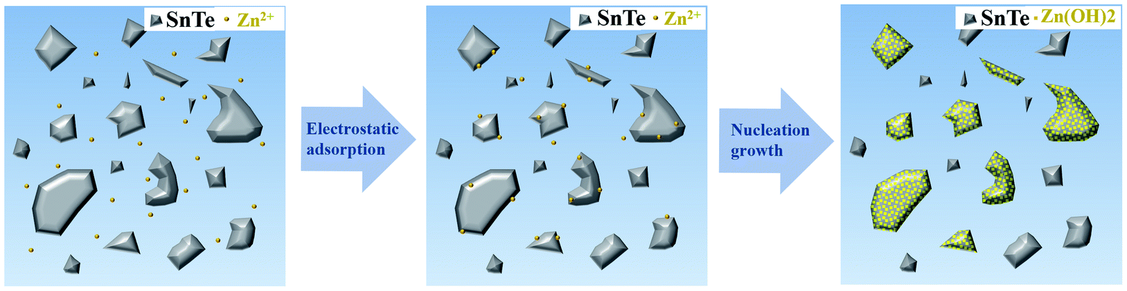 | ||
| Fig. 1 Schematic diagram of SnTe/ZnO core–shell particles in situ synthesis. | ||
 | ||
| Fig. 2 (a) XRD patterns of SnTe–x% ZnO (x = 0, 1, 1.5, 2.5) powders. (b) 2θ shift for SnTe–x% ZnO (x = 0, 1, 1.5, 2.5) powders. | ||
Fig. 3a displays the low-magnification SEM image of SnTe–1.5% ZnO powders, which shows that the grain size of hand-grinding SnTe particles distributes from dozens of nanometers to dozens of microns. Moreover, due to the low loading fraction of ZnO, the surface of only part of SnTe particles look rough and other SnTe particles are smooth. Thus, two large size particles with smooth and rough surface (Fig. 3b) are selected respectively for EDS characterization. As shown in Fig. 3c and d, EDS results demonstrate that Zn and O elements only exist in area A instead of area B, thus the surface in area A agrees with ZnO composition well. Besides, the surface of the SnTe particles became rough, which is due to the hydrolyzation of Zn2+ and subsequent dehydration.34
 | ||
| Fig. 3 (a) Low-magnification SEM image of the particles for SnTe–1.5% ZnO powders. (b) High-magnification SEM of the rough and smooth particles. (c and d) EDS spectrum of areas A and B in graph (b), respectively. | ||
The TEM images of Fig. 4a and b display the SnTe/ZnO core–shell particles, and it can be obviously seen that the SnTe surface was entirely coated with a floccule structure. Fig. 4c shows the HRTEM image along with the thin areas at the edge of the SnTe/ZnO core–shell particles. The lattice fringes with an interplanar spacing of 0.24 nm are the (101) plane of ZnO, indicating that ZnO nanosheets is successfully coated on the surface of SnTe. Thus, the existence of SnTe/ZnO core–shell structure is proved. Fig. 4d shows a high-angle annular dark-field scanning transmission electron microscopy (HAADF-STEM) image of a SnTe/ZnO core–shell particle, with a size of ∼4 μm. Moreover, the corresponding EDS mapping results of the SnTe/ZnO core–shell particle (Fig. 4d1–d4) clearly indicated that the Sn, Te, Zn, and O elements are homogeneously distributed, confirming the presence of SnTe/ZnO core–shell structure.
 | ||
| Fig. 4 (a and b) Low and medium magnification TEM images of SnTe/ZnO core–shell particles for SnTe–1.5% ZnO powders. (c) High-resolution TEM (HRTEM) image along with the thin areas at the edge of the SnTe/ZnO core–shell particle. (d) High-angle annular dark-field scanning transmission electron microscopy (HAADF-STEM) image of a SnTe/ZnO core–shell particle. (d1–d4) Elemental energy dispersive spectroscopy (EDS) mapping of graph (d). | ||
Fig. S3a and b† show the XRD patterns of SnTe–x% ZnO (x = 0, 1, 1.5, 2.5) bulks, suggesting that ZnO phase still exists in the SnTe matrix after SPS process. In order to characterize the morphology of ZnO nanosheets after SPS process, SEM and EDS are carried out, as shown in Fig. 5. Fig. 5a and b display the gradually magnified SEM images of the fractured of SnTe–1.5% ZnO bulks. It is found that there are many nano-dots with the size of 10–20 nm distributed around the grain boundary of SnTe. Moreover, the nano-dots are aggregated and well-attached to the surface of SnTe grains. To investigate the composition of the nano-dots above, EDS point scanning (Fig. 5c and d) is carried out, clearly indicating the obvious Zn and O peaks only appear in area B. Combining the results of SEM and EDS, it is speculated that the ZnO nanosheets coated on SnTe grains transform into ZnO nano-dots after SPS process. In the SPS process, the plasma generated by microscopic electrical discharge in the gaps between the powder particles will produce high temperature at the surface of the particles.35,36 When the temperature is high enough, the ZnO nanosheets will occur plastic deformation and transform into nanodots under the effect of the surface tension.
 | ||
| Fig. 5 (a and b) SEM images of the fractured surface of SnTe–1.5% ZnO. (c and d) EDS spectra of areas A and B in graph (b), respectively. | ||
To determine the spatial distribution of the elements, Fig. 6 gives the backscattered electron (BSE) and EDS mapping results on a polished surface of SnTe–1.5% ZnO sample. Fig. 6a clearly displays that the dark phase appears around the grey SnTe grain boundary, with a size of ∼4 μm, keeping a typical core–shell structure.37 The EDS mapping of this area presented in Fig. 6b exhibits the Sn, Te, Zn, and O distribution, respectively. The enrichment regions of bright areas in Zn and O EDS mapping correspond to the dark shell in graph (a), and the bright areas in Sn and Te EDS mapping consist with the grey phase in graph (a) as well. Thus, we can confirm that the composition of the dark shell agrees well with ZnO and the core is SnTe. Therefore, the SnTe/ZnO core–shell still exist after SPS process.
 | ||
| Fig. 6 (a) Backscattering scanning electron (BSE) images of polished surfaces of SnTe–1.5% ZnO (b) EDS mapping of graph (a). | ||
Fig. 7 shows the electrical conductivity σ, Seebeck coefficient S, power factor PF of SnTe–x% ZnO (x = 0, 1, 1.5, 2.5) bulks. As can be seen in Fig. 7a, the σ of all the samples experiences a great drop with the increment of temperature, exhibiting the characteristic of degenerate semiconductors. Meanwhile, the σ decreases greatly at the whole temperature region after constructing SnTe/ZnO core–shell structure, which can be explained by the sharp decrease of carrier concentration nH in the inset of Fig. 7b. For instance, the n decreases sharply from 1.6 × 1020 cm−3 for SnTe to 0.86 × 1020 cm−3 for SnTe–1% ZnO. To its surprise, the carrier mobility μ rises obviously to 519 cm2 V−1 s−1 for SnTe–1% ZnO, which is 132.7% higher than pristine SnTe. As shown in the Fig. 7d, due to ZnO is a wide band-gap semiconductor material, the difference of Fermi level, defects, and the lattice mismatch between the ZnO and SnTe form the energy barrier at the SnTe/ZnO heterogeneous interface.31,38 Such energy barrier will lead to the energy filtering effect by restraining the diffusion/drift of carriers with energy E lower than the barrier height Vb.29 Thus, the lower energy carriers will be filtered and high energy carriers will cross the energy barrier. Meanwhile, the average energy of carriers will be increased, which contributes to the increased μ.30,39,40 Moreover, the μ decreases slightly with the increasing ZnO content, which is opposite to that of nH.
 | ||
| Fig. 7 Electrical properties: (a) electrical conductivity, (b) Seebeck coefficient, and (c) power factor, as a function of temperature for SnTe–x% ZnO. (d) Schematic diagram of the carrier energy barrier at the heterogeneous interface of SnTe/ZnO core/shell; the inset graph of (b) shows the hole concentration and the carrier mobility of SnTe–x% ZnO at room temperature. | ||
It can be obviously observed in Fig. 7b that the S of all the samples is positive, indicating p-type conductions. The S of SnTe–x% ZnO (x = 1, 1.5, 2.5) samples is higher than the pristine SnTe when T > 573 K. For example, the S of the pristine SnTe increases from 18.55 μW cm−1 K−2 at 300 K to 117.79 μW cm−1 K−2 at 873 K while the S of SnTe–1.5% ZnO increases from 22.98 μW cm−1 K−2 at 300 K to 162.25 μW cm−1 K−2 at 873 K. Furthermore, the S increases with the increasing ZnO content, which is contrary to σ. The improvement of S can be attributed to the energy filtering effect caused by the SnTe/ZnO heterogeneous interface.31 The energy barrier can not only get the high energy carriers across but also filter low energy carriers, finally leading to the increased carrier effective mass m*.41 Thus, the S can be improved simultaneously. Due to the enhancement of S, the power factor PF of SnTe–x% ZnO samples is effectively improved as shown in Fig. 7c, and a maximum PF of 19.42 μW cm−1 K−2 at 873 K is obtained in SnTe–1.5% ZnO.
Fig. 8a shows the temperature-dependent total thermal conductivity κ for SnTe–x% ZnO (x = 0, 1, 1.5, 2.5) samples. The κ of all the samples decreases with the increase of temperature monotonously. Meanwhile, the κ drops sharply in the low/moderate temperature region but the tendency slows down in the high temperature region.42,43 The κ decreases remarkably after constructing SnTe/ZnO core–shell structure because of the simultaneous decrease of κe and κl. For instance, κ at the room temperature drops sharply to 6.83 W m−1 K−1 of SnTe–1.5% ZnO, which is 29.7% lower than the pristine SnTe. The electrical thermal conductivity κe (Fig. 8b) is calculated by the formula: κe = LσT. The κe experiences a sharp slump compared with the pristine SnTe and is in a downward trend with the increasing temperature. The decreasing tendency of the κe slows down in the high temperature region, which is of positive relevance with that of σ.
 | ||
| Fig. 8 Thermal properties: (a) thermal conductivity, (b) electronic thermal conductivity, (c) lattice thermal conductivity as a function of temperature for SnTe–x% ZnO samples. | ||
Fig. 8c shows the lattice thermal conductivity κl as a function of temperature for SnTe–x% ZnO (x = 0, 1, 1.5, 2.5) samples. The κl of SnTe–x% ZnO (x = 1, 1.5, 2.5) samples is dramatically lower than that of the SnTe below 673 K. For instance, the κl of SnTe–1.5% ZnO is 1.83 W m−1 K−1 at room temperature, which is 43.7% lower than the pristine SnTe. However, the κl of all ZnO-incorporated samples is higher than pristine SnTe when the temperature is over 673 K. Because the density of interface caused by SnTe/ZnO core–shell structure can only scatter low/medium frequency phonons and thus reduce κl in the low/medium temperature region.33,44 The heat transfer of high frequency phonons is dominated at high temperatures, so the effect of interfaces is weakened.43,45
Based on the results of thermal performance and electrical performance, the dimensionless figure of merit (ZT) can be obtained by utilizing the formula: ZT = S2σT/κ. Fig. 9 shows temperature dependence of ZT values for SnTe–x% ZnO (x = 0, 1, 1.5, 2.5) samples. Benefiting from simultaneously optimized PF and κ, a maximum ZT value of 0.67 is achieved in SnTe–1.5% ZnO at 873 K, which is 50% higher than pristine SnTe. Nevertheless, the minimum κl of SnTe–x% ZnO (∼1.83 W m−1 K−1) is far higher than the amorphous limit of SnTe (∼0.40 W m−1 K−1), motivating us to reduce κl by applying the other strategy.
 | ||
| Fig. 9 Temperature dependence of ZT values for SnTe–x% ZnO. | ||
To further improve the thermoelectric performance, we try to introduce massive point defects, including substitutional and interstitial defects to regulate the thermal performance of high temperature ends.46 Here, 3–6% mol of Cu2Te is chosen and alloyed with SnTe matrix to further reduce κl. Fig. 10a and b displays the XRD pattern of SnTe(Cu2Te)y–1.5% ZnO (y = 0.03, 0.04, 0.05, 0.06) bulks, the characteristic peaks can be indexed to rock-salt SnTe (Fm![[3 with combining macron]](https://www.rsc.org/images/entities/char_0033_0304.gif) m) structure. However, the Cu2Te diffraction peak can be detected when the Cu2Te content is over 0.03. For y = 0.03 sample, Cu2Te peaks cannot be detected by XRD measurements due to its low content.
m) structure. However, the Cu2Te diffraction peak can be detected when the Cu2Te content is over 0.03. For y = 0.03 sample, Cu2Te peaks cannot be detected by XRD measurements due to its low content.
 | ||
| Fig. 10 (a) XRD patterns of SnTe(Cu2Te)y–1.5% ZnO (y = 0.03, 0.04, 0.05, 0.06) bulks. (b) 2θ shifts for SnTe(Cu2Te)y–1.5% ZnO (y = 0.03, 0.04, 0.05, 0.06) bulks. | ||
The measurement temperature of thermoelectrical performance for SnTe(Cu2Te)y–1.5% ZnO (Fig. 11) is range from 300 K to 823 K, avoiding the deformation of samples above 823 K. Fig. 11a–c shows the temperature dependence of σ, S, and PF of SnTe(Cu2Te)y–1.5% ZnO samples. It is clearly observed in Fig. 11a that the σ drops slightly over the entire temperature region after Cu2Te alloying. As can be seen in Fig. 11b, Cu2Te-alloying samples exhibit a lower S when compared with Cu2Te-free sample in the low/medium temperature region, but exhibits a higher S at the high temperature end. Thus a peak S of 168.21 mV K−1 at 823 K was obtained for SnTe(Cu2Te)0.05–1.5% ZnO. The simultaneous decreasing of σ and S contributes to the degradation of PF (Fig. 11c) in the low/medium temperature region. However, in the high temperature region, the PF of Cu2Te-alloying samples is comparable to that of SnTe–1.5% ZnO, which is attributed to the fact that the enhancement of S compensates for the reduction of σ.
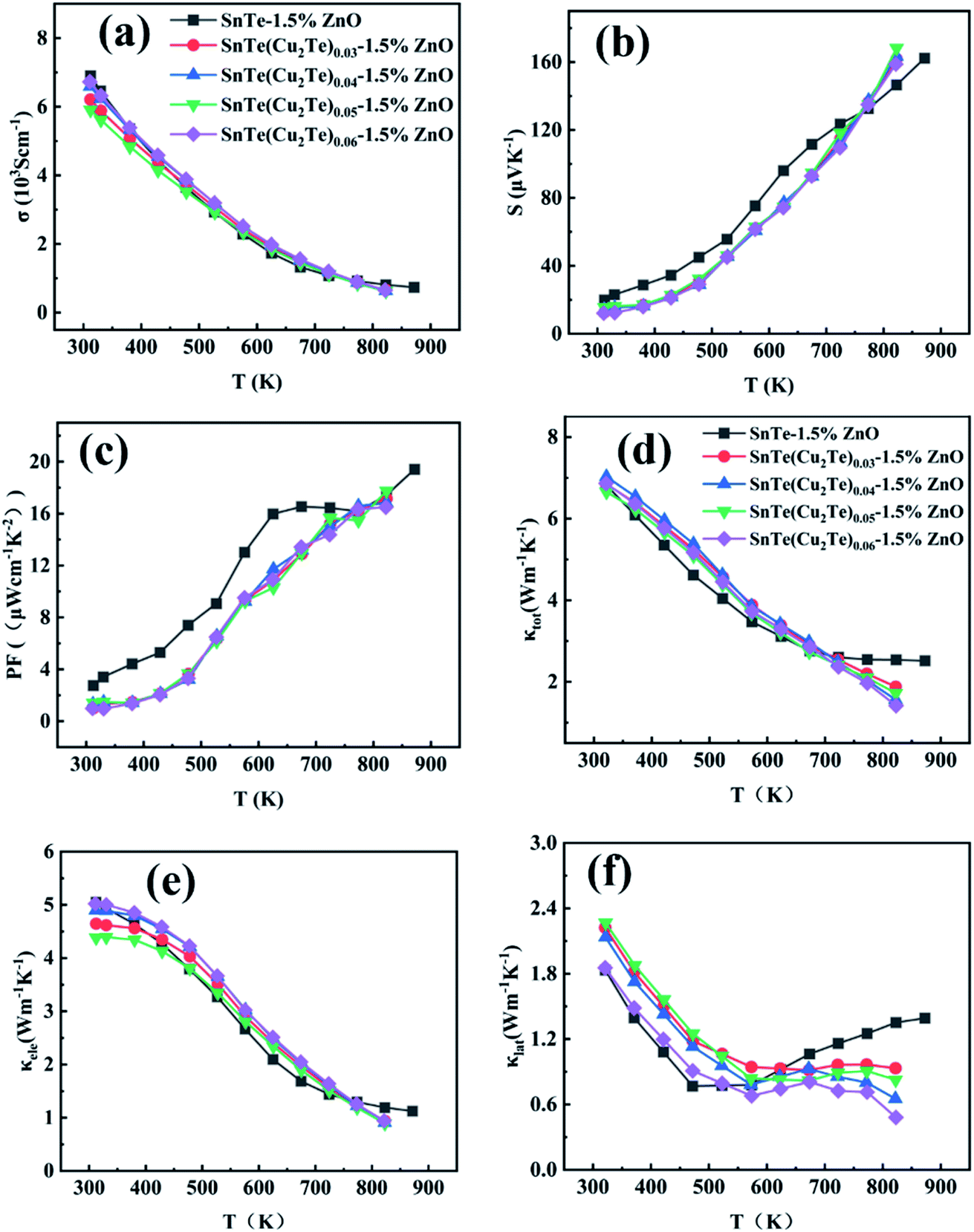 | ||
| Fig. 11 Electrical properties: (a) electrical conductivity, (b) Seebeck coefficient, and (c) power factor, as a function of temperature SnTe(Cu2Te)y–1.5% ZnO. Thermal properties: (d) thermal conductivity, (e) electronic thermal conductivity, (f) lattice thermal conductivity as a function of temperature for SnTe(Cu2Te)y–1.5% ZnO samples. | ||
Fig. 11d–f shows temperature dependence of κ, κe, and κl of SnTe(Cu2Te)y–1.5% ZnO samples. In Fig. 11d, the κ of Cu-alloying samples drops sharply in the high temperature region when compared with SnTe–1.5% ZnO, reaching the bottom of 1.42 W m−1 K−1 for SnTe(Cu2Te)0.06–1.5% ZnO at 823 K. The κe (Fig. 11e) of Cu2Te-alloying samples drops sharply at the high temperature end, comparing with the SnTe–1.5% ZnO sample. Fig. 11f indicates that the κl of Cu2Te-alloying samples decreases effectively above 600 K when compared with SnTe–1.5% ZnO, and the SnTe(Cu2Te)0.06–1.5% ZnO sample reaches the lowest κl of 0.48 W m−1 K−1 at 823 K, closing to the amorphous limit of SnTe.47 It is because the point defects via Cu2Te-alloying, including substitutional and interstitial defects, produce local mass and strain fluctuations in the matrix, which can scatter the high frequency phonons effectively.46,48
Fig. 12 displays temperature dependence of ZT values for the pristine SnTe and SnTe(Cu2Te)y–1.5% ZnO (y = 0, 0.03, 0.04, 0.05, 0.06) samples. The ZT value first increases from 0.45 in SnTe to 0.67 in SnTe–1.5% ZnO at 873 K after constructing SnTe/ZnO core–shell structure, and further increases through alloying SnTe matrix with Cu2Te, reaching the peak of ∼0.94 in SnTe(Cu2Te)0.06–1.5% ZnO at 823 K.
 | ||
| Fig. 12 Temperature dependence of ZT values for the pristine SnTe and SnTe(Cu2Te)y–1.5% ZnO samples. | ||
4. Conclusion
To sum up, a facile hydrothermal method is applied to in situ synthesize SnTe/ZnO core–shell particles. The energy filtering effect constructed by SnTe/ZnO core–shell structure significantly reduces the carrier concentration and improves the Hall mobility, finally leading to a peak power factor of 19.42 μW cm−1 K−2 for SnTe–1.5% ZnO at 873 K. Besides, the interfaces introduced by ZnO intensely scatter the low/medium frequency phonons, and a mass of point defects involved through Cu2Te-alloying strength the scattering of high frequency phonons successfully, which contributes to the lowest κl of 0.48 W m−1 K−1 in this work, closing to the amorphous limit. Finally, a peak ZT of 0.94 is achieved in SnTe(Cu2Te)0.06–1.5% ZnO at 823 K, which is 138% higher than that for the pristine SnTe. This work shows the feasibility of improving the TE performance by in situ synthesizing ZnO core–shell structure, and also has a referential value for other thermoelectric materials.Conflicts of interest
The authors declare that they have no known competing financial interests or personal relationships that could have appeared to influence the work reported in this paper.Acknowledgements
This work was supported by the National Natural Science Foundation of China (No. 52101220) and the Fundamental Research Funds for the Central Universities (JZ2021HGTA0155, JZ2021HGQA0189).References
- F. J. Disalvo, Science, 1999, 285, 703–706 CrossRef CAS PubMed.
- R. Moshwan, L. Yang, J. Zou and Z. G. Chen, Adv. Funct. Mater., 2017, 27, 1703278 CrossRef.
- J. W. Zhang, Z. W. Wu, F.-P. Zhang, X. Y. Yang and J. X. Zhang, J. Electron. Mater., 2021, 50, 649–656 CrossRef CAS.
- Y. Wang, L. Yang, X. L. Shi, X. Shi, L. Chen, M. S. Dargusch, J. Zou and Z. G. Chen, Adv. Mater., 2019, 31, 1807916 CrossRef PubMed.
- L. Yang, Z. G. Chen, M. S. Dargusch and J. Zou, Adv. Energy Mater., 2018, 8, 1701797 CrossRef.
- Z. Chen, J. Li, J. Tang, F. Zhang, Y. Zhong, H. Liu and R. Ang, J. Mater. Sci. Technol., 2021, 89, 45–51 CrossRef CAS.
- Y. Luo, S. Cai, S. Hao, F. Pielnhofer, I. Hadar, Z. Z. Luo, J. Xu, C. Wolverton, V. P. Dravid, A. Pfitzner, Q. Yan and M. G. Kanatzidis, Joule, 2020, 4, 159–175 CrossRef CAS.
- Y. Luo, Z. Ma, S. Hao, S. Cai, Z. Z. Luo, C. Wolverton, V. P. Dravid, J. Yang, Q. Yan and M. G. Kanatzidis, J. Am. Chem. Soc., 2022, 144, 1445–1454 CrossRef CAS PubMed.
- Z. Bu, X. Zhang, B. Shan, J. Tang, H. Liu, Z. Chen, S. Lin, W. Li and Y. Pei, Sci. Adv., 2021, 7, eabf2738 CrossRef CAS PubMed.
- Y. Luo, T. Xu, Z. Ma, D. Zhang, Z. Guo, Q. Jiang, J. Yang, Q. Yan and M. G. Kanatzidis, J. Am. Chem. Soc., 2021, 143, 13990–13998 CrossRef CAS PubMed.
- K. Imasato, C. Fu, Y. Pan, M. Wood, J. J. Kuo, C. Felser and G. J. Snyder, Adv. Mater., 2020, 32, 1908218 CrossRef CAS PubMed.
- L. Su, D. Wang, S. Wang, B. Qin, Y. Wang, Y. Qin, Y. Jin, C. Chang and L. D. Zhao, Science, 2022, 375, 1385–1389 CrossRef CAS PubMed.
- S. Liu, Y. Yu, D. Wu, X. Xu, L. Xie, X. Chao, M. Bosman, S. J. Pennycook, Z. Yang and J. He, Adv. Funct. Mater., 2021, 31, 2007340 CrossRef CAS.
- V. Prokopiv, M. O. Galushchak, I. V. Horichok, T. Parashchuk, O. Matkivskiy, V. V. Bachuk and R. O. Dzumedzey, Phys. Chem. Solid State, 2019, 20, 149–155 CrossRef CAS.
- G. Tan, L. D. Zhao, F. Shi, J. W. Doak, S. H. Lo, H. Sun, C. Wolverton, V. P. Dravid, C. Uher and M. G. Kanatzidis, J. Am. Chem. Soc., 2014, 136, 7006–7017 CrossRef CAS PubMed.
- W. Li, Y. Wu, S. Lin, Z. Chen, J. Li, X. Zhang, L. Zheng and Y. Pei, ACS Energy Lett., 2017, 2, 2349–2355 CrossRef CAS.
- M. Zhou, Z. M. Gibbs, H. Wang, Y. Han, C. Xin, L. Li and G. J. Snyder, Phys. Chem. Chem. Phys., 2014, 16, 20741–20748 RSC.
- J. D. I. Masek and D. Nuzhnyj, Acta Phys. Pol., 1997, 92, 915–918 CrossRef CAS.
- X. Dong, W. Cui, W. D. Liu, S. Zheng, L. Gao, L. Yue, Y. Wu, B. Wang, Z. Zhang, L. Chen and Z. G. Chen, J. Mater. Sci. Technol., 2021, 86, 204–209 CrossRef CAS.
- D. G. Cahill, S. K. Watson and R. O. Pohl, Phys. Rev. B, 1992, 46, 6131–6140 CrossRef CAS PubMed.
- A. Banik, U. Shenoy, S. Anand, U. Waghmare and K. Biswas, Chem. Mater., 2014, 27, 581–587 CrossRef.
- G. Tan, F. Shi, J. W. Doak, H. Sun, L. D. Zhao, P. Wang, C. Uher, C. Wolverton, V. P. Dravid and M. G. Kanatzidis, Energy Environ. Sci., 2015, 8, 267–277 RSC.
- G. Tan, F. Shi, S. Hao, H. Chi, L. D. Zhao, C. Uher, C. Wolverton, V. P. Dravid and M. G. Kanatzidis, J. Am. Chem. Soc., 2015, 137, 5100–5112 CrossRef CAS PubMed.
- J. He, X. Tan, J. Xu, G. Q. Liu, H. Shao, Y. Fu, X. Wang, Z. Liu, J. Xu, H. Jiang and J. Jiang, J. Mater. Chem. A, 2015, 3, 19974–19979 RSC.
- H. Deng, X. Lou, W. Lu, J. Zhang, D. Li, S. Li, Q. Zhang, X. Zhang, X. Chen, D. Zhang, Y. Zhang and G. Tang, Nano Energy, 2021, 81, 105649 CrossRef CAS.
- K. Biswas, J. He, G. Wang, S. H. Lo, C. Uher, V. P. Dravid and M. G. Kanatzidis, Energy Environ. Sci., 2011, 4, 4675–4684 RSC.
- Q. Zhang, B. Liao, Y. Lan, K. Lukas, W. Liu, K. Esfarjani, C. Opeil, D. Broido, G. Chen and Z. Ren, Proc. Natl. Acad. Sci. U. S. A., 2013, 110, 13261–13266 CrossRef CAS PubMed.
- M. Bachmann, M. Czerner and C. Heiliger, Phys. Rev. B, 2012, 86, 115320 CrossRef.
- D. Narducci, S. Frabboni and X. Zianni, J. Mater. Chem. C, 2015, 3, 12176–12185 RSC.
- Z. Ma, C. Wang, J. Lei, D. Zhang, Y. Chen, Y. Wang, J. Wang and Z. Cheng, Nanoscale, 2020, 12, 26 CrossRef PubMed.
- Z. Zhou, J. Yang, Q. Jiang, D. Zhang, J. Xin, X. Li, Y. Ren and X. He, J. Am. Ceram. Soc., 2017, 100, 5723–5730 CrossRef CAS.
- J. Zhang, S. Li, Z. Zhu, Z. Wu and J. Zhang, Dalton Trans., 2021, 50, 10515–10523 RSC.
- J. Zhang, S. Li, Z. Wu and J. Zhang, J. Alloys Compd., 2021, 889, 161651 CrossRef.
- Z. Wang, B. Cheng, L. Zhang, J. Yu and H. Tan, Sol. RRL, 2022, 6, 2100587 CrossRef CAS.
- J. Li, T. Zhang, C. Han, H. Li, R. Shi, J. Tong and B. Li, J. Mater. Chem. A, 2019, 7, 455–460 RSC.
- Z. H. Zhang, Z. F. Liu, J. F. Lu, X. B. Shen, F. C. Wang and Y. D. Wang, Scr. Mater., 2014, 81, 56–59 CrossRef CAS.
- S. Li, J. Xin, A. Basit, Q. Long, S. Li, Q. Jiang, Y. Luo and J. Yang, Adv. Sci., 2020, 7, 1903493 CrossRef CAS PubMed.
- K. C. Kim, S.-S. Lim, S. H. Lee, J. Hong, D. Y. Cho, A. Y. Mohamed, C. M. Koo, S. H. Baek, J. S. Kim and S. K. Kim, ACS Nano, 2019, 13, 7146–7154 CrossRef CAS PubMed.
- Z. Ma, C. Wang, Y. Chen, L. Li, S. Li, J. Wang and H. Zhao, Mater. Today Phys., 2021, 17, 100350 CrossRef CAS.
- L. Fu, J. Yang, J. Peng, Q. Jiang, Y. Xiao, Y. Luo, D. Zhang, Z. Zhou, M. Zhang, Y. Cheng and F. Cheng, J. Mater. Chem. A, 2015, 3, 1010–1016 RSC.
- T. Hong, C. Guo, D. Wang, B. Qin, C. Chang, X. Gao and L. D. Zhao, Mater. Today Energy, 2022, 25, 100985 CrossRef CAS.
- S. K. Kihoi, U. S. Shenoy, J. N. Kahiu, H. Kim, D. K. Bhat and H. S. Lee, ACS Sustainable Chem. Eng., 2022, 10, 1367–1372 CrossRef CAS.
- Y. Pei and D. T. Morelli, Appl. Phys. Lett., 2009, 94, 122112 CrossRef.
- X. Zhang, Y. Zhou, Y. Pei, Y. Chen, B. Yuan, S. Zhang, Y. Deng, S. Gong, J. He and L. D. Zhao, J. Alloys Compd., 2017, 709, 575–580 CrossRef CAS.
- Z. Chen, B. Ge, W. Li, S. Lin, J. Shen, Y. Chang, R. Hanus, G. J. Snyder and Y. Pei, Nat. Commun., 2017, 8, 13828 CrossRef CAS PubMed.
- Y. Pei, L. Zheng, W. Li, S. Lin, Z. Chen, Y. Wang, X. Xu, H. Yu, Y. Chen and B. Ge, Adv. Electron. Mater., 2016, 2, 1600019 CrossRef.
- J. W. Zhang, Z. W. Wu, B. Xiang, N. N. Zhou, J. L. Shi and J. X. Zhang, ACS Appl. Mater. Interfaces, 2020, 12, 21863–21870 CrossRef CAS PubMed.
- F. Guo, B. Cui, H. Geng, Y. Zhang, H. Wu, Q. Zhang, B. Yu, S. J. Pennycook, W. Cai and J. Sui, Small, 2019, 15, 1902493 CrossRef PubMed.
Footnote |
| † Electronic supplementary information (ESI) available. See https://doi.org/10.1039/d2ra04255j |
| This journal is © The Royal Society of Chemistry 2022 |