
 Open Access Article
 This Open Access Article is licensed under a
 Creative Commons Attribution 3.0 Unported Licence
Introduction of cadmium chloride additive to improve the performance and stability of perovskite solar cells
Mustafa K. A. Mohammed *aj,
Majid S. Jabirb,
Haider G. Abdulzahraac,
Safa H. Mohammedd,
Waleed Khaild Al-Azzawie,
Duha S. Ahmed*b,
Sangeeta Singh*f,
Anjan Kumarfg,
S. Asaithambih and
Masoud Shekargoftari
*aj,
Majid S. Jabirb,
Haider G. Abdulzahraac,
Safa H. Mohammedd,
Waleed Khaild Al-Azzawie,
Duha S. Ahmed*b,
Sangeeta Singh*f,
Anjan Kumarfg,
S. Asaithambih and
Masoud Shekargoftari
aRadiology Techniques Department, Dijlah University College, Al-Masafi Street, Baghdad 00964, Iraq. E-mail: mustafa_kareem97@yahoo.com; Tel: +964-7719047121
bApplied Science Department, University of Technology, Iraq
cDepartment of Prosthodontic, Dijlah University College, Al-Masafi Street, Baghdad, Iraq
dRadiological Techniques Department, Al-Mustaqbal University College, Babylon, Iraq
eDepartment of Medical Instruments Engineering Techniques, Al-Farahidi University, Baghdad, Iraq
fMicroelectronics Lab, National Institute of Technology, Patna 800005, India
gVLSI Research Lab, GLA University, Mathura-281406, India
hDepartment of Physics, Alagappa University, Karaikudi, 630 003, Tamil Nadu, India
iLaboratory for Biomaterials and Bioengineering (CRC-I), Department of Min-Met-Materials Engineering, Laval University, Quebec City, QC G1V0A6, Canada
jUniversity of Warith Al-Anbiyaa, Karbala, Iraq
First published on 15th July 2022
Abstract
With the increase in the importance of using green energy sources to meet the world's energy demands, attempts have been made to push perovskite solar cell technology toward industrialization all around the world. Improving the properties of perovskite materials as the heart of PSCs is one of the methods to fabricate favorable photovoltaic (PV) solar cells based on perovskites. Here, cadmium chloride (CdCl2) was used as an additive source for the perovskite precursor to improve its PV properties. Results indicated CdCl2 improves the perovskite growth and tailors its crystalline properties, suggesting boosted charge transport processes in the bulk and interfaces of the perovskite layer with electron–hole transport layers. Overall, by incorporation of 1.0% into the MAPbI3 layer, a maximum power conversion efficiency of 15.28% was recorded for perovskite-based solar cells, higher than the 12.17% for the control devices. The developed method not only improved the PV performance of devices but also boosted the stability behavior of solar cells due to the passivated domain boundaries and enhanced hydrophobicity in the CdCl2-based devices.
1. Introduction
Due to their exceptional photoelectric performance and easy fabrication processes, hybrid perovskite solar cells (HPSCs) have attracted considerable attention as a promising candidate for new-generation photovoltaic (PV) devices.1–3 This could be related to the high absorption coefficient, high charge transfer phenomenon, and adjustable bandgap along with high charge diffusion length, which are all important requirements.4–6 The efficiency of HPSCs has substantially increased from a low of 3.8% (in 2009)7 to a verified 25.2% (in 2021),8 which has encouraged researchers in the HPSC's future development. Typically, according to the direction of the photocurrent, the fundamental architecture of HPSCs can be categorized into conventional (n–i–p) and inverted (p–i–n) architectures.9,10 It's worth mentioning that the perovskite material is the heart of an HPSC device, and its overall quality determines how well it performs. The power conversion efficiency (PCE), hysteresis, and long-term stability of HPSCs are all influenced by the morphology, crystalline nature, and surface covering of the perovskite film.11–13 A high content of pinholes and grain boundaries (GBs) in the perovskite film, particularly, produces severe shorting and trap centers for non-radiative recombination, which is one of the primary sources of PCE degradation in HPSCs.14,15 Charge recombination aided by pinholes and GBs is also associated with abnormal hysteresis and instability concerns. As a result, enhancing the perovskite properties via passivating defects and optimizing perovskite quality has become a critical technique for decreasing recombination rates, removing unfavorable hysteresis, prolonging HPSC longevity, and increasing PCE.16,17To date, several ways of controlling perovskite morphology have been explored, involving manipulating the deposition method, additive engineering, interfacial engineering, and compositional engineering.18–22 Additive engineering has been shown to be effective in improving the quality of the perovskite layer since it is a more simple and reproducible approach. Some agents, including copper chloride, N,1-diiodoformamidine, potassium hexafluorophosphate, formamidine acetate salt, etc., can form an intermediate phase with perovskite precursors, which could regulate the dynamic process of crystal formation and thereby minimize GBs.23–27 The incorporation of cadmium (Cd2+) additive by Suneth et al. was a fundamental advance in controlling methylammonium lead iodide (MAPbI3) crystallinity using a two-step deposition method. With this treatment, the efficiency of MAPbI3-based HPSCs was significantly boosted from 7.1 to 13.8%.28 Yong et al. reported the addition of Cd2+ into organic–inorganic cation-based CsxFA1−xPbI3 lattice to enhance the crystallinity and the charge carrier lifetime of perovskite film. An efficiency up to 20.59% was achieved for HPSC with a structure of ITO glass/SnO2/CsxFA1−xPbI3/spiro-OMeTAD/Au.29 In another study, a suppression of atomic vacancies via strain relaxation of CsMAFA triple-cation perovskite film was reported by Makhsud et al. This suppression was achieved via incorporation of Cd isovalent small ions, which let to boost the stability of HPSCs in ambient air.30 Recently, Cd2+ introduced into all-inorganic perovskite for carbon-based HPSCs with a framework of FTO/SnO2/CsPbIBr2/carbon. They demonstrated that Cd ions improves the crystalline nature and morphological merits of perovskite film, resulting in better optical absorption and carrier transfer in perovskite with less recombination rates. Also, in compared to the HPSCs without Cd2+ doping (4.36%), the improved HPSCs attained the highest PCE of 6.79%.31 Yi et al. introduced ammonium benzenesulfonate as a passivator into the MAPbI3 solution to assist the film crystallization and mitigate trap density. A champion PCE of 20.6% is obtained for the modified HPSCs.32 Hua et al. reported the incorporation of N,1-diiodoformamidine modifier into FAMAPbI3 to improve the quality of perovskite with bigger grain size and fewer defects, hence improving the PCE from 19.07% to 21.22% as well as their light and thermal stabilities.24 Recently, a dual additive approach for enhancing the performance of HPSCs was reported by Yang et al.33 The highest PCE of 23.2% is yielded via a mixed modifier of MACl/CsCl with a 2![[thin space (1/6-em)]](https://www.rsc.org/images/entities/char_2009.gif) :1 ratio, which is better than that for a single modifier of MACl or CsCl. Despite their high performance, the majority of HPSCs fabricated with organic hole transport layers (HTLs) such as spiro-OMeTAD have low stability and are excessively expensive, making them unsuitable for commercialization. Therefore, further work is needed to find a cheaper alternative to spiro-OMeTAD while simultaneously utilizing the additive engineering approach.
:1 ratio, which is better than that for a single modifier of MACl or CsCl. Despite their high performance, the majority of HPSCs fabricated with organic hole transport layers (HTLs) such as spiro-OMeTAD have low stability and are excessively expensive, making them unsuitable for commercialization. Therefore, further work is needed to find a cheaper alternative to spiro-OMeTAD while simultaneously utilizing the additive engineering approach.
Herein, we take advantage of using an efficient additive of cadmium chloride (CdCl2) alongside with using a copper phthalocyanine (CuPc) semiconductor as a model HTL for regular (n–i–p) HPSCs. CuPc is known to possess high hole mobility, excellent interfacial bonding features, and superb stability while also being relatively inexpensive, which is why it has been used as a p-type semiconductor in different optoelectronic devices.34–36 We investigate the impact of employing low CdCl2 concentrations and high MAI contents during MAPbI3 development in the anti-solvent deposition procedure. In addition to better crystalline phase and increased grain size, steady-state photoluminescence (PL) tests revealed a significant reduction in charge recombination process. The best-performing CdCl2-based HPSCs using a CuPc HTL yielded a PCE of 15.28% with a VOC of 1.0 V and a FF of 73.2%, recorded under reverse scanning. The modified devices demonstrated enhanced long-term stability as compared to unmodified devices fabricated with mesoscopic structures.
2. Experimental part
2.1 Materials
All solvents, titanium isopropoxide (TTIP, 97%), cadmium chloride (CdCl2, 99.99%), lithium bis(trifluoromethylsulfonyl)imide salt (LiTFSI, 98%), and copper phthalocyanine (CuPc, 99%) were provided from Sigma-Aldrich. Lead iodide (PbI2, 99.99%), methylammonium iodide (MAI, 99.5%), and 2,2′,7,7′-tetrakis(N,N-di-p-methoxyphenylamino)-9,9′-spirobifluorene (spiro-OMeTAD, 99.8%) were prepared from LumTec. TiO2 paste was prepared from Dyesol.2.2 Solution preparation
922 mg of PbI2 were dissolved in 1.27 mL of N,N-dimethylformamide (DMF, 99.8%) and 0.142 mL dimethyl sulfoxide (DMSO, 99.8%). The resultant product was mixed at 80 °C for 45 min. After cooling down the PbI2 solution, 318 mg of MAI was inserted into it and stirred for 15 min to prepare MAPbI3. For incorporation of CdCl2 into the perovskite layer, different amounts of CdCl2 in molar ratios to MAI are added into the prepared perovskite solutions, followed by further stirring at RT for 60 min. 500 mg of TiO2 paste is dissolved in 3.0 g ethanol (EtOH, 99.8%) and is stirred at RT for 24 h to attain mesoporous TiO2 (mp-TiO2) solution. 700 mg of TTIP is added into 10 mL of 2-propanol (IPA, 99.9%) containing 70 μL of 2 M HCl, followed by stirring in an ice bath for 30 min to prepare compact TiO2 (c-TiO2) precursor. The spiro-OMeTAD precursor was prepared as reported in the literature of (ref. 37) by dissolving 36.2 mg of spiro-OMeTAD (99%) in 500 μL chlorobenzene (CB, 99.9%) doped with LiTFSI, and 4-tert-butylpyridine (98%).2.3 HPSC fabrication
Transparent conductive F-doped SnO2 (FTO, Pilkington) glasses with a sheet resistance of 15 Ω sq−1 are ultrasonically cleaned with distilled water, soap, distilled water, acetone, and IPA successively for 10 min. 45 μL of the c-TiO2 solution is spread in each FTO piece and spin-coated at 4000 rpm, followed by annealing at 500 °C for 30 min to fabricate a c-TiO2 layer. 60 μL of mp-TiO2 precursor is spin-coated on each c-TiO2 layer at 4000 rpm for 30 s, followed by baking at 450 °C for 60 min. To fabricate perovskite layer, 60 μL of perovskite precursors with or without CdCl2 additive are spread on each substrate and spin coated at 1000 rpm for 8 s and then accelerate up to 6000 for 30 s. During the faster step, 200 μL of CB was pipetted on perovskite layer to assist crystal growth of perovskite layer. Perovskite layers were annealed for 30 min at 100 °C. The CuPc hole transport layer (HTL) with thickness of 30 nm was thermally evaporated on the pre-formed perovskite films in a vacuum of 10−3 Pa with deposition rate of 1 Å s−1. To fabricate spiro-OMeTAD HTL, its precursor was spin-coated at 5000 rpm for 30 s on top the perovskites. Finally, a 100 nm gold thin-layer was thermally deposited the HTLs.2.4 Characterizations
A Mira3, TESCAN field emission scanning electron microscopy (FESEM) was used to monitor the effect of the CdCl2 additive on the micro-morphology of perovskite layers. A Bruker, D8 Advance X-ray diffractometer was used to collect XRD pattern of perovskite films. A LAMBDA 1050 spectrophotometer was used to study the light-harvesting ability of perovskite layers. A HORIBA Fluorolog-III spectrometer with an exciting wavelength at 405 nm was used to record steady-state photoluminescence (PL) responses of perovskite layers. Photovoltaic performance of MAPbI3-based solar cells with an active area of 2 mm × 3 mm was characterized using a Keithley Model 2401 under a calibrated AM 1.5 light simulator to record current density–voltage curves. A calibrated Newport IPCE equipment was employed to record incident photon-to-electron conversion efficiency (IPCE) of solar cells.3. Results and discussion
Fig. 1 presents the FESEM micrographs of the perovskites prepared with and without the CdCl2 additives in the MAI precursors that were utilized to complete the MAPbI3 conversion. The influence of the CdCl2 incorporation is clear in that good uniformity and large grains are observed in the CdCl2-added perovskites immediately after heat treatment (Fig. 1b and c), while film deposited without solvent additive shows low uniformity and small grains with obvious pinholes at the grain edges (Fig. 1a). As illustrated in Fig. 1e–h, the addition of small amounts of CdCl2 enlarged the average grain size fivefold, from 280 nm to 590 nm. This is due to the inclusion of CdCl2 into the MAI solution, which produces Cl ions, resulting in the formation of an intermediate phase that acts as a seed and enhances the development of bigger MAPbI3 crystals.38 With a further increase of CdCl2 amount to 1.5%, the surface of the perovskite layer was identical to the 1% CdCl2-added film but revealed small particles with obvious grain boundaries (GBs). From the FESEM results, we can argue that the grain size of the CdCl2-modified films was not greatly enlarged. Nevertheless, smaller grains have combined into bigger ones, the gaps between grains have been passivated, and the film has become denser and more compact. This could help improve HPSC performance by reducing nonradiative charge recombination.39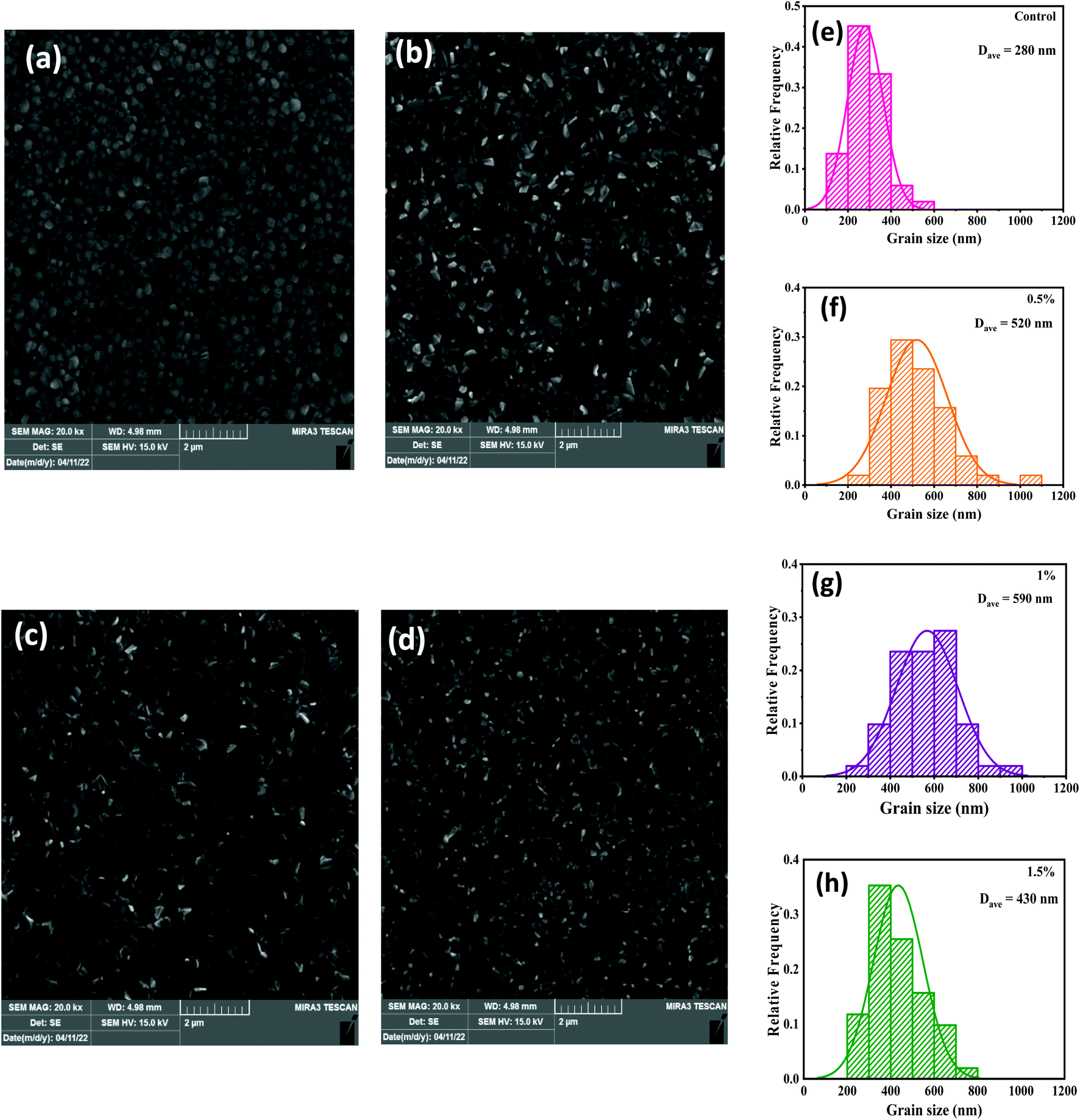 | ||
| Fig. 1 The top-view FESEM visualization of perovskite layers with (a) 0%, (b) 0.5%, (c) 1%, and (d) 1.5% of CdCl2 in perovskite precursors. Substrate for all layers was FTO/c-TiO2/mp-TiO2. (e–h) Particle size distributions of perovskite films evaluated by ImageJ software. | ||
The performance of HPSCs is directly dependent on the crystal phase and purity of the MAPbI3 layers.40 Fig. 2a demonstrates the X-ray patterns of MAPbI3 perovskites without and with 1% CdCl2 inclusion into the MAI solution. As demonstrated, multiple main XRD peaks at 13.82°, 20.10°, 28.18°, and 31.59° were indexed as (110), (112), (220), and (310) planes of the tetragonal MAPbI3 phase, respectively.21 The sharp and intensive peaks in the XRD plots of the MAPbI3 perovskites implied that the films were well crystallized. Furthermore, the intensities of the prominent peaks all rose when the CdCl2 solvent was incorporated, implying that a superior crystalline nature and larger crystallite size for perovskite film were developed as compared to a film prepared without CdCl2.41 In MAPbI3 samples prepared without and with CdCl2, the full width at half maximum intensity of the (110) peak was 0.108 and 0.097, respectively. According to the Scherrer equation,42 the average crystallite sizes of the corresponding samples were 73.46 and 81.21 nm, respectively. These findings suggest that the moderate amount of CdCl2 in perovskite could increase both crystallinity and grain size. This result is also in line with the findings of the FESEM images.
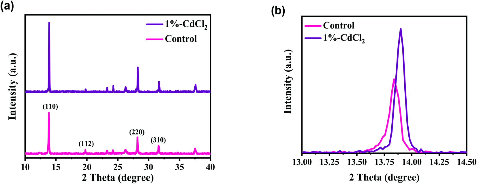 | ||
| Fig. 2 (a) XRD patterns of perovskite layers without (control) and with 1% of CdCl2 deposited on FTO/c-TiO2/mp-TiO2 substrate. (b) Zoomed XRD patterns around 2θ = 13.9°. | ||
The low XRD signal at 12.4° is indexed as the cubic PbI2, because of the slight degradation of the MAPbI3 to PbI2 and/or incomplete crystallization of perovskite.23 The presence of PbI2 in the perovskite would be detrimental to photo-induced carrier transfer, lowering film stability and increasing the hysteresis behavior of HPSCs. Interestingly, it was apparently seen that the typical peak of PbI2 was completely removed with CdCl2 treatment. Fig. 2b shows the XRD patterns of perovskite samples zoomed to the major (110) peaks. The (110) peak was altered to higher values of 2θ with the addition of CdCl2. This is most likely owing to a variation in the lattice parameters caused by the replacement of smaller Cd2+ species for Pb2+ sites,28 therefore leading to the shrinkage of the MAPbI3 lattice. The reduced lead amounts in perovskite could be beneficial for increasing the tolerance factor, improves the stability of the MAPbI3 structure.31
We used UV-vis absorption and PL spectroscopy to explore the influence of the CdCl2 solvent on light absorption and the mechanism of photoexcited carriers transport in perovskite film deposited under the same conditions unless the variation in CdCl2 concentrations in MAI solution. The UV-vis spectra of MAPbI3 perovskite layers with various concentrations of CdCl2 additive are shown in Fig. 3a. The absorbance plots measured for MAPbI3 layers with and without CdCl2 treatments exhibited remarkably identical absorption profiles (edge-absorption position at 777 nm) thanks to the unique energy bandgap (Eg) absorption of MAPbI3 as a sunlight harvester.43 As we can see, all samples fabricated by the spin-coating clearly show strong absorbance over the full light absorption below 700 nm. When the concentration of CdCl2 solution is raised to 1%, the absorption performance of the associated MAPbI3 layer slightly increases within the visible range. This could be due to the increased grain size and improved crystallinity, while the film thickness remains similar with the insertion of CdCl2.44 However, when more CdCl2 (1%) was introduced, the perovskite's light absorption capacity dropped because the presence of unwanted defects and GBs disrupted the film's compact structure. Fig. 3b describes the Tauc plots for all samples prepared with and without CdCl2 additives. The value of Eg can be evaluated by extrapolating the variation between photo energy (hν) and (αhν)2.45 The values of Eg were found to be 1.59 eV, which is similar to the values reported in the literature.13,40
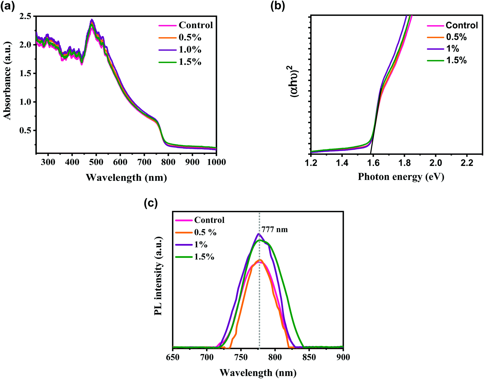 | ||
| Fig. 3 (a) UV-vis absorption spectra, (b) Tauc plots, and (c) photoluminescence spectra of control and modified perovskite layers with different amounts of CdCl2, deposited on glass substrates. | ||
Fig. 3c shows the steady-state PL measurements of perovskite films spin-coated on glass substrates without HTL and ETL films in order to reduce charge extraction at the interfaces and enable the inherent features of the MAPbI3 film to govern the recombination dynamics. All the steady-state PL plots of perovskites reveal a typical and strong luminescence peak at locations identical to the absorbance edges detected in UV-vis measurements. The increased PL intensity and reduced linewidth of CdCl2-treated films in comparison to the control layer indicate that the incorporation of solvent additive can significantly inhibit trap-mediated, non-radiative recombination in those perovskites.46 This could be due to the CdCl2 additive treatments improving the crystallinity of the developed perovskites. The enhanced crystalline structure decreased defects in the entire MAPbI3, resulting in fewer recombination taps in the film. This inhibited the non-radiation recombination pathway, making it more suitable for optoelectronics manufacturing. Conversely, as the CdCl2 concentration was increased to 1.5%, the PL intensity of the perovskite decreased, indicating an increase in the density of microstructural defects.
We fabricated regular (n–i–p) HPSC devices using the architecture of glass/FTO/c-TiO2/mp-TiO2/MAPbI3/CuPc/Au, as illustrated in Fig. 4a. The ETL films are fabricated based on our previously prepared mp-TiO2 via the spin-coating method, while HTLs utilize a p-type inorganic film named CuPc. The mixed solutions of MAI:PbI2 were used to form perovskite film with an anti-solvent assistance approach. An additive engineering method was employed in our perovskite films to improve the HPSC performance. The CdCl2 additive was selected as a modifier to assist perovskite crystallization during the deposition process. We have investigated the PV parameters of our designed HPSCs with reverse J–V sweep being performed under the AM 1.5 sunlight simulator. Fig. 4b demonstrates the best-performing J–V plots of the HPSCs fabricated with and without additive treatments, and the summarized cell parameters are displayed in Table 1. The performance of HPSCs with and without CdCl2 additives varies significantly. Without CdCl2, the HPSCs show low PV performances with a JSC of 19.78 mA cm−2, VOC of 0.962 V, FF of 65.70% and, a champion PCE of 12.17%. The HPSC has an enhanced PCE of 15.28% with a high JSC of 20.87 mA cm−2, a VOC of 1.00 V, and a good FF of 73% after adding 1% CdCl2. When the amount of CdCl2 is increased to 1.5%, the PCE of the HPSC has a notable reduction to 14.10% with reduced JSC and practically unchanged VOC. As previously mentioned, an adequate dose of CdCl2 modifier can assist in removing PbI2 residual without forming a non-perovskite phase, resulting in a compact high-quality layer with large crystals, which can greatly reduce interior recombination and enhance HPSC performance. The integrated JSC values of the unmodified and 1% CdCl2-based HPSCs are 19.08 mA cm−2 and 20.14 mA cm−2, respectively, as shown in Fig. 4c, which match with the JSC values determined from the detailed J–V scan characteristics. The IPCE measurements confirm the accuracy of our HPSC efficiency characterizations.
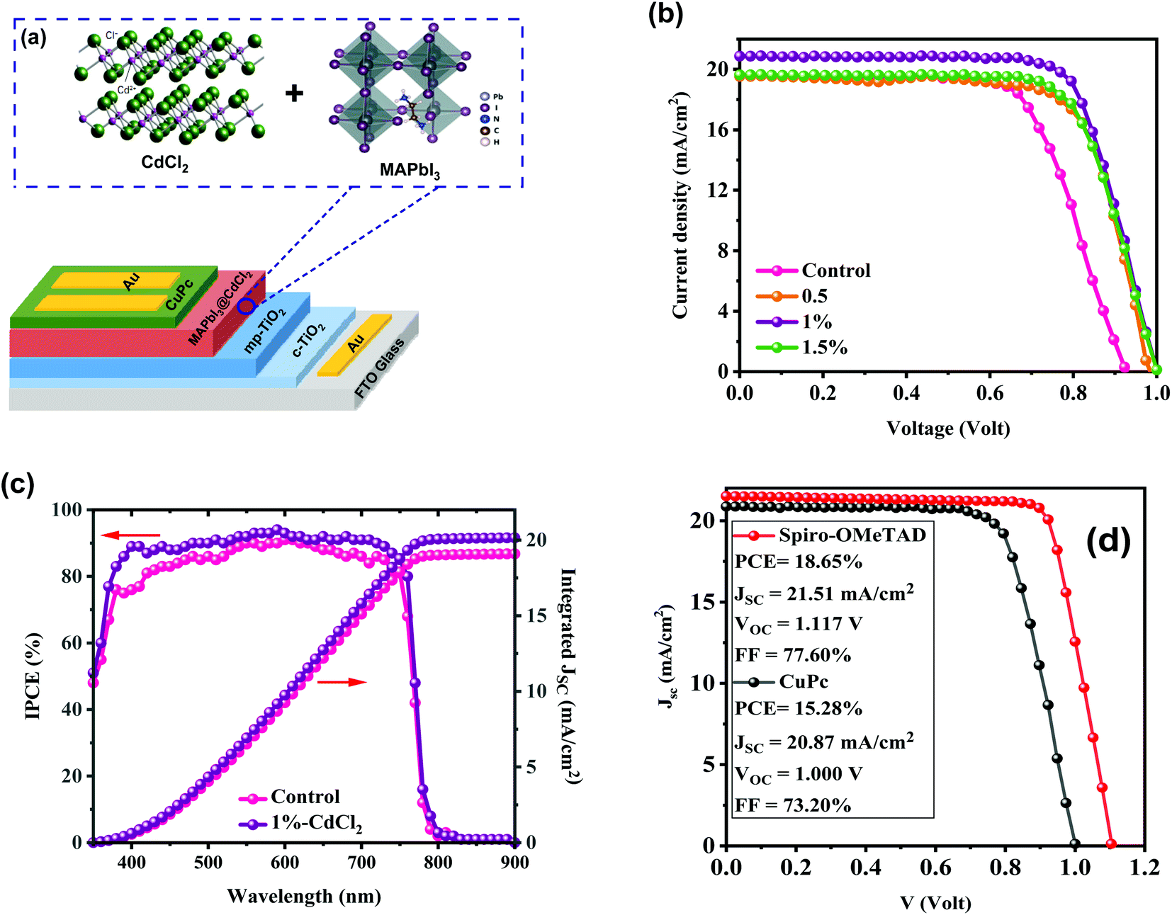 | ||
| Fig. 4 (a) Schematic diagram of the device architecture of CdCl2-assisted deposition process for MAPbI3 film. (b) J–V curves of the best-performing HPSCs with different amounts of CdCl2 additive. (c) Recorded IPCE responses of the control and modified device with 1% of CdCl2 and their integrated JSC from the IPCE. (d) J–V curves of perovskite solar cells with copper phthalocyanine (CuPc) and 2,2′,7,7′-tetrakis(N,N-di-p-methoxyphenylamino)-9,9′-spirobifluorene (spiro-OMeTAD) as hole transport layers. | ||
| CdCl2 amount | VOCa (V) | JSCb (mA cm−2) | FFc (%) | PCE (%) | |
|---|---|---|---|---|---|
| a VOC is open-circuit voltage.b JSC is short-circuit current density.c FF is fill factor. | |||||
| Control | Average | 0.946 ± 0.018 | 19.16 ± 0.48 | 63.26 ± 2.75 | 11.44 ± 0.63 |
| Best | 0.962 | 19.78 | 65.70 | 12.17 | |
| 0.5% | Average | 0.964 ± 0.019 | 19.48 ± 0.55 | 69.15 ± 1.97 | 12.98 ± 0.52 |
| Best | 0.987 | 19.54 | 71.70 | 13.82 | |
| 1.0% | Average | 0.994 ± 0.007 | 20.33 ± 0.41 | 72.29 ± 1.34 | 14.61 ± 0.43 |
| Best | 1.000 | 20.87 | 73.20 | 15.28 | |
| 1.5% | Average | 0.985 ± 0.013 | 19.23 ± 0.53 | 69.68 ± 1.29 | 13.19 ± 0.50 |
| Best | 1.000 | 19.64 | 71.80 | 14.10 | |
To compare the performance of CuPc-based PSCs with conventional spiro-OMeTAD PSCs, we fabricated PSCs with spiro-OMeTAD HTL. A champion PCE of 18.65% with a JSC of 21.51 mA cm−2, VOC of 1.117 mV, and FF of 77.60% was obtained (Fig. 4d). It notes that CuPc can be considered a low-cost HTL in perovskite-based solar cells. The CuPc HTL recorded a JSC near to spiro-OMeTAD devices, with lower VOC and FF than spiro-OMeTAD HTL one. Finding refers that recording higher PCE with CuPc HTL is reachable by more engineering at the interface of perovskite/CuPc, which will be targeted in our future experiments.
Fig. 5 depicts the distribution of PV parameters depending on the concentration of MAI to CdCl2, where the ratio of MAI:CdCl2 is changed from 0% to 1.5%. As shown in Fig. 5a, adjusting the ratio has a notable effect on the mean JSC of nearly 20 mA cm−2. VOC improves slightly with increasing the CdCl2 concentration (Fig. 5b). The average VOC value of 0.946 V for the control device is increased to 0.964, 0.994, and 0.985 V as the ratio varies from 0% to 1.5%. Mean FF is also enhanced as the concentration of CdCl2 increases, reaching 72.29% at 1% and then decreasing to 69.68% at 1.5% (Fig. 5c). As a consequence, PCE is boosted from 11.44% for the control device to 14.61% for the 1% CdCl2-modified device (Fig. 5d). Also, the statics show the narrow distribution of PV parameters of HPSCs based on the optimized 1% CdCl2, indicating excellent reproducibility of solar cells.
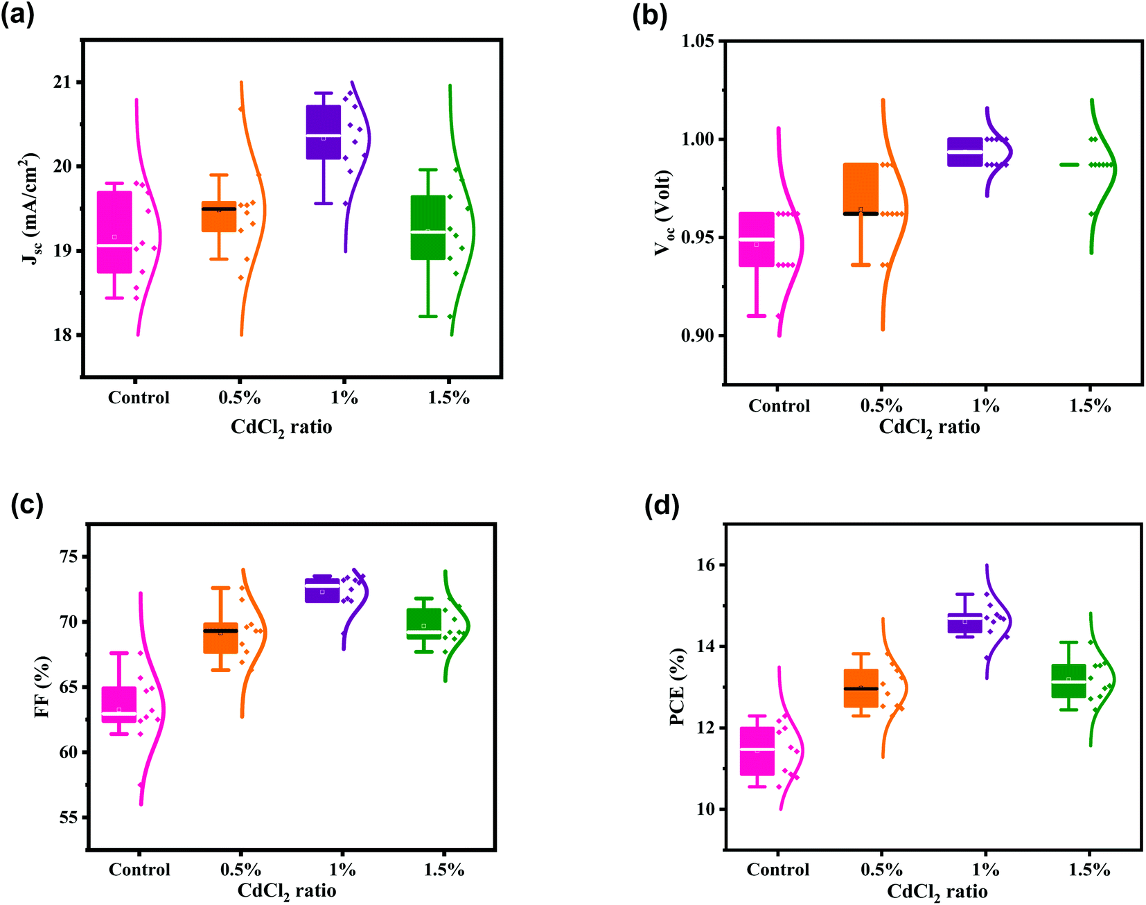 | ||
| Fig. 5 (a–d) Statistics of the PCE, JSC, VOC and FF for HPSCs modified with different amounts of CdCl2 additive. PV parameters collected from 10 devices for each set. | ||
To further study the role of CdCl2 material on the PV properties of space-charge-limited current (SCLC) measurements for electron-only devices with a structure of FTO/c-TiO2/mp-TiO2/MAPbI3 with or without CdCl2/PCBM/Au were investigated. The electron trap density (Nt) of the perovskites layers were calculated as follows:47
 | (1) |
 40 Compared with the control PSCs with a HI value of 11.99%, the 1% CdCl2-modified PSCs showed a HI of 2.87%. The weaken HI in the CdCl2-based PSCs can be attributed to the passivated domain boundaries in the modified perovskite layer. In addition, as SCLC results showed, CdCl2 incorporation into the perovskite layer accelerates electron transfer within the bulk of perovskite layer and suppresses HI in the PSCs.48,49
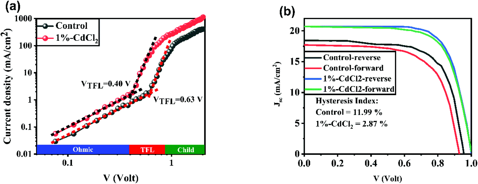 | ||
| Fig. 6 (a) J–V curves of electron-only of control and 1%-CdCl2 perovskite solar cells devices. (b) J–V curves of a perovskite solar cell device with or without of CdCl2 additive in reverse and forward scan directions. | ||
One of the most critical performance factors for future commercial uses of HPSCs is long-term stability. Therefore, the HPSC longevity of related MAPbI3-based regular HPSCs (unmodified and with 1% CdCl2) was assessed by tracing the PCE progression under ambient conditions with a RH of 25–40% in the dark (see Fig. 7). After 2040 h of age, the PCEs of the HPSC with 1% CdCl2 additive demonstrate outstanding stability, maintaining 83% of the original value. In contrast, the performances of the unmodified HPSC dropped to less than 59% of their initial values after 2040 h, mainly attributable to perovskite degradation. Hence, the incorporation of CdCl2 in MAPbI3-based HPSCs, results in outstanding PV parameters and environmental stability.
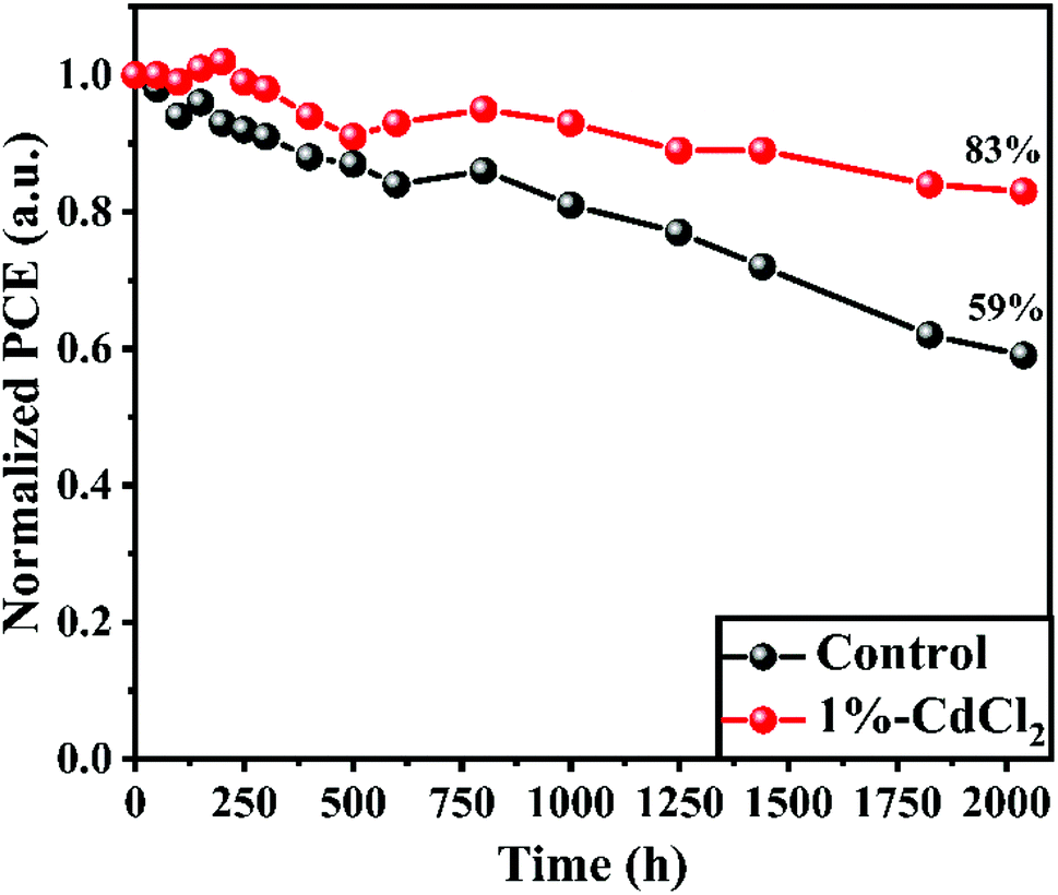 | ||
| Fig. 7 Stability test of the unsealed control perovskite solar cells stored in ambient conditions with a relative humidity (RH) of 25–40%. | ||
4. Conclusion
In conclusion, we have proven a simple method based on additive engineering to improve the PCE and stability of MAPbI3-based HPSCs by adding a certain concentration of CdCl2 additive. The impacts of varying concentrations of CdCl2 additives on perovskite layer characteristics and PV properties were studied. High crystallinity, large grain size, improved optical absorption ability, and fewer pinholes and GBs were obtained for perovskite film fabricated with the optimized CdCl2 concentration, resulting in excellent photovoltaic performance. The synergistic influence of crystal growth control and pinhole passivation by CdCl2 effectively decreases the charge carrier recombination. With the incorporation of 1% CdCl2 into the MAI solution, the HPSC yielded a champion PCE of over 15.28% under the reverse scan conditions. In comparison with unmodified HPSC, the HPSC based on 1% CdCl2 also shows excellent ambient stability, which maintained 83% of its initial PCE after being stored for 2040 h without encapsulation. Our findings indicate that CdCl2 is a good additive for making inexpensive HPSCs with excellent stability.Conflicts of interest
The authors declare no conflict of interest.References
- M. K. Mohammed, 21.4% efficiency of perovskite solar cells using BMImI additive in the lead iodide precursor based on carbon nanotubes/TiO2 electron transfer layer, Ceramics Inter., 2020, 46(17), 27647–27654 CrossRef CAS.
- K. Kim, Z. Wu, J. Han, Y. Ma, S. Lee, S. K. Jung, J. W. Lee, H. Y. Woo and I. Jeon, Homogeneously Miscible Fullerene inducing Vertical Gradient in Perovskite Thin-Film toward Highly Efficient Solar Cells, Adv. Energy Mater., 2022, 2200877 CrossRef CAS.
- S. H. Kareem, M. H. Elewi, A. M. Naji, D. S. Ahmed and M. K. Mohammed, Efficient and stable pure α-phase FAPbI3 perovskite solar cells with a dual engineering strategy: additive and dimensional engineering approaches, Chem. Eng. J., 2022, 136469 CrossRef.
- Y. Ding, B. Ding, H. Kanda, O. J. Usiobo, T. Gallet, Z. Yang, Y. Liu, H. Huang, J. Sheng and C. Liu, Single-crystalline TiO2 nanoparticles for stable and efficient perovskite modules, Nat. Nanotechnol., 2022, 1–8 Search PubMed.
- H. T. Hussein, R. S. Zamel, M. S. Mohamed and M. K. Mohammed, High-performance fully-ambient air processed perovskite solar cells using solvent additive, J. Phys. Chem. Solids, 2021, 149, 109792 CrossRef CAS.
- M. K. Mohammed, A. E. Shalan, M. Dehghanipour and H. Mohseni, Improved mixed-dimensional 3D/2D perovskite layer with formamidinium bromide salt for highly efficient and stable perovskite solar cells, Chem. Eng. J., 2022, 428, 131185 CrossRef CAS.
- A. Kojima, K. Teshima, Y. Shirai and T. Miyasaka, Organometal halide perovskites as visible-light sensitizers for photovoltaic cells, J. Am. Chem. Soc., 2009, 131(17), 6050–6051 CrossRef CAS PubMed.
- G.-H. Kim and D. S. Kim, Development of perovskite solar cells with >25% conversion efficiency, Joule, 2021, 5(5), 1033–1035 CrossRef.
- Z. Li, B. Li, X. Wu, S. A. Sheppard, S. Zhang, D. Gao, N. J. Long and Z. Zhu, Organometallic-functionalized interfaces for highly efficient inverted perovskite solar cells, Science, 2022, 376(6591), 416–420 CrossRef CAS PubMed.
- S. Zouhair, S. M. Yoo, D. Bogachuk, J. P. Herterich, J. Lim, H. Kanda, B. Son, H. J. Yun, U. Würfel and A. Chahboun, Employing 2D-Perovskite as an Electron Blocking Layer in Highly Efficient (18.5%) Perovskite Solar Cells with Printable Low Temperature Carbon Electrode, Adv. Energy Mater., 2022, 2200837 CrossRef CAS.
- M. K. Mohammed, M. Dehghanipour, U. Younis, A. E. Shalan, P. Sakthivel, G. Ravi, P. H. Bhoite and J. Pospisil, Improvement of the interfacial contact between zinc oxide and a mixed cation perovskite using carbon nanotubes for ambient-air-processed perovskite solar cells, New J. Chem., 2020, 44(45), 19802–19811 RSC.
- A. E. Shalan, M. K. Mohammed and N. Govindan, Graphene assisted crystallization and charge extraction for efficient and stable perovskite solar cells free of a hole-transport layer, RSC Adv., 2021, 11(8), 4417–4424 RSC.
- A. K. Al-Mousoi and M. K. Mohammed, Engineered surface properties of MAPI using different antisolvents for hole transport layer-free perovskite solar cell (HTL-free PSC), J. Sol-Gel Sci. Technol., 2020, 96(3), 659–668 CrossRef CAS.
- D. Luo, R. Su, W. Zhang, Q. Gong and R. Zhu, Minimizing non-radiative recombination losses in perovskite solar cells, Nat. Rev. Mater., 2020, 5(1), 44–60 CrossRef CAS.
- G. Nagaraj, M. K. Mohammed, M. Shekargoftar, P. Sasikumar, P. Sakthivel, G. Ravi, M. Dehghanipour, S. Akin and A. E. Shalan, High-performance perovskite solar cells using the graphene quantum dot-modified SnO2/ZnO photoelectrode, Mater. Today Energy, 2021, 22, 100853 CrossRef CAS.
- F. Gao, Y. Zhao, X. Zhang and J. You, Recent progresses on defect passivation toward efficient perovskite solar cells, Adv. Energy Mater., 2020, 10(13), 1902650 CrossRef CAS.
- C. C. Boyd, R. Cheacharoen, T. Leijtens and M. D. McGehee, Understanding degradation mechanisms and improving stability of perovskite photovoltaics, Chem. Rev., 2018, 119(5), 3418–3451 CrossRef.
- Z. Arain, C. Liu, Y. Yang, M. Mateen, Y. Ren, Y. Ding, X. Liu, Z. Ali, M. Kumar and S. Dai, Elucidating the dynamics of solvent engineering for perovskite solar cells, Sci. China Mater., 2019, 62(2), 161–172 CrossRef CAS.
- C. Chen, Z. Zhou, Y. Jiang, Y. Feng, Y. Fang, J. Liu, M. Chen, J. Liu, J. Gao and S.-P. Feng, Additive Engineering in Antisolvent for Widening the Processing Window and Promoting Perovskite Seed Formation in Perovskite Solar Cells, ACS Appl. Mater. Interfaces, 2022, 14(15), 17348–17357 CrossRef CAS.
- L. Chao, T. Niu, W. Gao, C. Ran, L. Song, Y. Chen and W. Huang, Solvent Engineering of the Precursor Solution toward Large-Area Production of Perovskite Solar Cells, Adv. Mater., 2021, 33(14), 2005410 CrossRef CAS.
- M. K. Mohammed, H. G. Abdulzahraa, S. Singh, P. Sasikumar and M. S. Jabir, Lithium chloride-based interface engineering at electron transport and perovskite layers to boost the performance of perovskite photovoltaics, Opt. Mater., 2022, 127, 112348 CrossRef CAS.
- L. Shen, Y. Yang, T. Zhu, L. Liu, J. Zheng and X. Gong, Efficient and Stable Perovskite Solar Cells by B-Site Compositional Engineered All-Inorganic Perovskites and Interface Passivation, ACS Appl. Mater. Interfaces, 2022, 14(17), 19469–19479 CrossRef CAS PubMed.
- E. Kayesh, K. Matsuishi, T. H. Chowdhury, R. Kaneko, T. Noda and A. Islam, Enhanced photovoltaic performance of perovskite solar cells by copper chloride (CuCl2) as an additive in single solvent perovskite precursor, Electron. Mater. Lett., 2018, 14(6), 712–717 CrossRef.
- H. Li, G. Wu, W. Li, Y. Zhang, Z. Liu, D. Wang and S. Liu, Additive engineering to grow micron-sized grains for stable high efficiency perovskite solar cells, Adv. Sci., 2019, 6(18), 1901241 CrossRef CAS PubMed.
- C. Gao, H. Dong, X. Bao, Y. Zhang, A. Saparbaev, L. Yu, S. Wen, R. Yang and L. Dong, Additive engineering to improve the efficiency and stability of inverted planar perovskite solar cells, J. Mater. Chem. C, 2018, 6(30), 8234–8241 RSC.
- Y. Liu, Y. Gao, M. Lu, Z. Shi, W. Y. William, J. Hu, X. Bai and Y. Zhang, Ionic additive engineering for stable planar perovskite solar cells with efficiency >22%, Chem. Eng. J., 2021, 426, 130841 CrossRef CAS.
- F. Zhang and K. Zhu, Additive engineering for efficient and stable perovskite solar cells, Adv. Energy Mater., 2020, 10(13), 1902579 CrossRef CAS.
- S. C. Watthage, Z. Song, N. Shrestha, A. B. Phillips, G. K. Liyanage, P. J. Roland, R. J. Ellingson and M. J. Heben, Enhanced grain size, photoluminescence, and photoconversion efficiency with cadmium addition during the two-step growth of CH3NH3PbI3, ACS Appl. Mater. Interfaces, 2017, 9(3), 2334–2341 CrossRef CAS.
- Y. Chen, Y. Zhao, Q. Ye, Z. Chu, Z. Yin, X. Zhang and J. You, Improved efficiency and photo-stability of methylamine-free perovskite solar cells via cadmium doping, J. Semicond., 2019, 40(12), 122201 CrossRef CAS.
- M. I. Saidaminov, J. Kim, A. Jain, R. Quintero-Bermudez, H. Tan, G. Long, F. Tan, A. Johnston, Y. Zhao and O. Voznyy, Suppression of atomic vacancies via incorporation of isovalent small ions to increase the stability of halide perovskite solar cells in ambient air, Nat. Energy, 2018, 3(8), 648–654 CrossRef CAS.
- R. Wang, H. Zhang, S. Han, Y. Wu, Z. Hu, G. Zhang, H. Liu, Q. He and X. Zhang, Cadmium doping for improving the efficiency and stability of carbon-based CsPbIBr2 all-inorganic perovskite solar cells, New J. Chem., 2021, 45(20), 9243–9250 RSC.
- Y. Yang, H. Peng, C. Liu, Z. Arain, Y. Ding, S. Ma, X. Liu, T. Hayat, A. Alsaedi and S. Dai, Bi-functional additive engineering for high-performance perovskite solar cells with reduced trap density, J. Mater. Chem. A, 2019, 7(11), 6450–6458 RSC.
- I. S. Yang and N. G. Park, Dual additive for simultaneous improvement of photovoltaic performance and stability of perovskite solar cell, Adv. Funct. Mater., 2021, 31(20), 2100396 CrossRef CAS.
- T. Duong, J. Peng, D. Walter, J. Xiang, H. Shen, D. Chugh, M. Lockrey, D. Zhong, J. Li and K. Weber, Perovskite solar cells employing copper phthalocyanine hole-transport material with an efficiency over 20% and excellent thermal stability, ACS Energy Lett., 2018, 3(10), 2441–2448 CrossRef CAS.
- X. Jiang, D. Wang, Z. Yu, W. Ma, H. B. Li, X. Yang, F. Liu, A. Hagfeldt and L. Sun, Molecular engineering of copper phthalocyanines: a strategy in developing dopant-free hole-transporting materials for efficient and ambient-stable perovskite solar cells, Adv. Energy Mater., 2019, 9(4), 1803287 CrossRef.
- Y.-Y. Ma, X.-C. Hua, T.-S. Zhai, Y.-H. Li, X. Lu, S. Duhm and M.-K. Fung, Doped copper phthalocyanine via an aqueous solution process for high-performance organic light-emitting diodes, Org. Electron., 2019, 68, 236–241 CrossRef CAS.
- M. Dehghanipour, A. Behjat, A. Shabani and M. Haddad, Toward desirable 2D/3D hybrid perovskite films for solar cell application with additive engineering approach, J. Mater. Sci.: Mater. Electron., 2022, 1–12 Search PubMed.
- S. T. Williams, F. Zuo, C.-C. Chueh, C.-Y. Liao, P.-W. Liang and A. K.-Y. Jen, Role of chloride in the morphological evolution of organo-lead halide perovskite thin films, ACS Nano, 2014, 8(10), 10640–10654 CrossRef CAS PubMed.
- S. Jin, Y. Wei, X. Yang, D. Luo, Y. Fang, Y. Zhao, Q. Guo, Y. Huang, L. Fan and J. Wu, Additive engineering induced perovskite crystal growth for high performance perovskite solar cells, Org. Electron., 2018, 63, 207–215 CrossRef CAS.
- M. Dehghanipour, A. Behjat and H. A. Bioki, Fabrication of stable and efficient 2D/3D perovskite solar cells through post-treatment with TBABF4, J. Mater. Chem. C, 2021, 9(3), 957–966 RSC.
- Z. Zhou, X. Li, M. Cai, F. Xie, Y. Wu, Z. Lan, X. Yang, Y. Qiang, A. Islam and L. Han, Stable inverted planar perovskite solar cells with low-temperature-processed hole-transport bilayer, Adv. Energy Mater., 2017, 7(22), 1700763 CrossRef.
- S. Asaithambi, P. Sakthivel, M. Karuppaiah, R. Yuvakkumar, K. Balamurugan, T. Ahamad, M. M. Khan, G. Ramalingam, M. K. Mohammed and G. Ravi, Preparation of Fe-SnO2@CeO2 nanocomposite electrode for asymmetric supercapacitor device performance analysis, J. Energy Storage, 2021, 36, 102402 CrossRef.
- M. M. Tavakoli, M. Saliba, P. Yadav, P. Holzhey, A. Hagfeldt, S. M. Zakeeruddin and M. Grätzel, Synergistic crystal and interface engineering for efficient and stable perovskite photovoltaics, Adv. Energy Mater., 2019, 9(1), 1802646 CrossRef.
- X. Hou, S. Huang, W. Ou-Yang, L. Pan, Z. Sun and X. Chen, Constructing efficient and stable perovskite solar cells via interconnecting perovskite grains, ACS Appl. Mater. Interfaces, 2017, 9(40), 35200–35208 CrossRef CAS.
- D. S. Ahmed, M. R. Mohammed and M. K. Mohammed, Synthesis of multi-walled carbon nanotubes decorated with ZnO/Ag nanoparticles by co-precipitation method, Nanosci. Nanotechnol.--Asia, 2020, 10(2), 127–133 CrossRef CAS.
- Y. Guo, W. Sato, K. Shoyama, H. Halim, Y. Itabashi, R. Shang and E. Nakamura, Citric acid modulated growth of oriented lead perovskite crystals for efficient solar cells, J. Am. Chem. Soc., 2017, 139(28), 9598–9604 CrossRef CAS PubMed.
- X. Liu, J. He, P. Wang, Y. Liu, J. Xiao, Z. Ku, Y. Peng, F. Huang, Y. B. Cheng and J. Zhong, Fabrication of Efficient and Stable Perovskite Solar Cells in High-Humidity Environment through Trace-Doping of Large-Sized Cations, ChemSusChem, 2019, 12(11), 2385–2392 CAS.
- Z. Tang, T. Bessho, F. Awai, T. Kinoshita, M. M. Maitani, R. Jono, T. N. Murakami, H. Wang, T. Kubo and S. Uchida, Hysteresis-free perovskite solar cells made of potassium-doped organometal halide perovskite, Sci. Rep., 2017, 7(1), 1–7 CrossRef PubMed.
- H. Mohseni, M. Dehghanipour, N. Dehghan, F. Tamaddon, M. Ahmadi, M. Sabet and A. Behjat, Enhancement of the photovoltaic performance and the stability of perovskite solar cells via the modification of electron transport layers with reduced graphene oxide/polyaniline composite, Sol. Energy, 2021, 213, 59–66 CrossRef CAS.
| This journal is © The Royal Society of Chemistry 2022 |