 Open Access Article
Independently tunable all-dielectric synthetic multi-spectral metamaterials based on Mie resonance
Yeqing Zhua,
Xi Tiana,
Jiukai Fanga,
Yanpeng Shi *a,
Shengnan Shia,
Shan Zhanga,
Jinmei Songa,
Meiping Lia,
Xiaoyu Liua,
Xiaodong Wang
 b and
Fuhua Yangb
aSchool of Microelectronics, Shandong University, Jinan 250100, China. E-mail: ypshi@sdu.edu.cn
bEngineering Research Center for Semiconductor Integrated Technology, Institute of Semiconductors, Chinese Academy of Sciences, Beijing 100083, China
First published on 20th July 2022
Abstract
A single metamaterial (MM) is generally designed to operate in only one band, and the MMs with different dimensions of meta-atoms are required to be integrated to achieve multi-spectral responses simultaneously. In this study, an all-dielectric synthetic multi-spectral metamaterial (SMM) that can efficiently operate in the visible and terahertz (THz) ranges by incorporating nanoscale features into microscale unit cells is demonstrated and investigated numerically. The resonant frequency of the proposed SMM in both regimes can be tuned independently by changing the geometric parameters such as diameter, gap, width and height of unit cells functional in two different regions, whilst maintaining high reflectance efficiency. Results show that a variety of colors can be produced from red to purple in the visible range with maximal reflectance as high as 83% while the peak frequency of the SMM can be adjusted from 8.12 to 2.13 THz in the THz range with maximum reflectance up to 94%. The reflection characteristics of the SMM mainly originate from the electric dipole (ED) and magnetic dipole (MD) resonances via Mie scattering in both regions. The strategy of this research offers the possibility of applications in bio/chemical sensing, multi-spectral imaging, filtering, detection, modulation and so on.
1. Introduction
Metamaterials (MMs) are artificially constructed materials composed of subwavelength periodic meta-atoms which exhibit unusual electromagnetic properties impossible to achieve with natural materials, such as negative refractive index,1,2 electromagnetic induced transparency3,4 and invisibility.5,6 Owing to their unique properties and the rapid blossoming of fabrication techniques, MMs operating from RF to optics have been achieved by adjusting the structural units appropriately and employed to realize diverse applications, including filters,7,8 absorbers,9,10 polarization converters11 and modulators.12,13 However, most of the reported MMs can only interact with electromagnetic waves in one band, imposing undesirable restrictions on their application in certain areas such as multi-spectral imaging, which requires collecting discrete information distributed over multiple spectral ranges so as to acquire more features from the object of interest.14,15 For another example, benefiting from the abundant electromagnetic modalities and the strong enhancement of local fields, MM is very sensitive to surrounding dielectric environment changes, making it suitable for bio/chemical sensing applications.16,17 Researchers have proposed various approaches to achieve MM based sensors,18–21 however, these sensors can typically detect molecules within only one specific frequency region. MMs with multi-band adaptability are required for simultaneous monitoring of diverse targeted analytes that possess spectral signatures located in different frequency bands.Accordingly, it would be meaningful to achieve multi-spectral MMs capable of supporting resonant responses at two or more totally different spectral ranges of the electromagnetic spectrum. Traditionally, most of the MMs are constructed with metallic unit cells because they can exhibit many unique properties such as surface plasmon resonance,22,23 thus achieving effective regulation of the amplitude, phase and polarization of electromagnetic waves. Despite undisputed advantages, as the application of MM moves toward high frequencies, the performances of MMs based on metallic components are limited due to the large ohmic loss and fabrication difficulties, especially in the optical frequencies.24,25 For example, Grant et al.26 has presented a synthetic multi-spectral metamaterial (SMM) by hybridising optical plasmonic filtering with mid infrared (MIR) and terahertz (THz) MM absorption, thereby manipulating radiation in multiple regions at the same time. Nevertheless, the use of metallic components in this device leads to a decrease in visible and near infrared (NIR) transmission magnitude, which is further degraded by the MIR and THz electric ring resonators deposited above the nanohole array. To tackle the obstacles, MMs composed of all-dielectric building blocks have attracted rapidly growing research attention because of the better feasibility of fabrication and low dielectric loss in contrast to their metallic counterparts and various devices with specific functions are developed.27–30 On the other hand, the spectral tunability is an important factor affecting the performance of the MM. A single dual-region MM based on meander line resonators has been reported by Manjunath et al.31 The MM produced in this work can be functional in both THz and NIR frequencies simultaneously. Although the THz resonant frequency can be adjusted by increasing the gap between meta-atoms while having a negligible impact on the NIR transmission spectrum, the NIR resonant frequency cannot be tuned independently without affecting the THz response. To the best of our knowledge, all-dielectric multi-spectral MM operating over totally different wavebands with independently adjustable resonant response and high efficiency has not been presented previously.
In this paper, an all-dielectric SMM is proposed with the capability of efficiently operating in two completely different regimes simultaneously, that is the visible and THz ranges. As is well-known, the construction of MMs, instead of the composition, dictates their electromagnetic characteristics. With the size of the meta-atom varying from millimeter to nanometer scales, the response region of the MM transfers accordingly from microwaves to the visible frequencies. In consequence, we incorporate arrays of Si nanodisk resonators into microscale unit cells to combine multi-spectral capabilities into a single SMM. Once they are combined, the obtained SMM exhibits a similar Mie resonant response in aforementioned two regimes. The resonant mechanism of the designed SMM is interpreted by providing the electromagnetic field distributions at reflection peaks. It should also be noted that wide adjustment of the resonant frequency of the SMM in both regions can be achieved independently by varying geometric parameters of Si nanodisk arrays and microscale unit cells, whilst still maintaining high reflectance efficiency. A variety of colors can be produced covering almost the entire visible spectrum in the optical frequency band with maximal reflectance of 83% while the peak frequency of the SMM can be adjusted from 8.12 to 2.13 THz in the THz region with maximum reflectance of 94%. As a result, the proposed design is expected to pave the way for applications ranging from bio/chemical sensing, multi-spectral imaging, filtering, detection to modulation and can also achieve flexible manipulation of the object color appearance to satisfy people's aesthetic or functional requirements.32,33
2. Structural design and numerical simulation
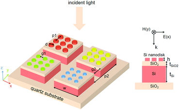
The SMM is designed and optimized by performing simulations using the finite difference time domain (FDTD) solutions. Fig. 1 shows the schematic of the proposed SMM built on a quartz substrate and its geometrical parameters. In microscale THz unit cell, there are plenty of subunit cells functional in visible wavelength to generate various required colors. The cross-sectional view of a single unit cell used in the SMM is illustrated in the right panel, where a SiO2 dielectric spacer is sandwiched between an array of Si nanodisk and a Si layer below. The height (h) of the nanodisk, the thickness of the SiO2 spacer (tSiO2) and the Si layer (tSi) are set to 100 nm, 360 nm and 15.9 μm respectively. The nanodisk diameter (d), period (p1) and gap (g1), the width (w), period (p2) and gap (g2) of the unit cell are also marked in the diagram.In order to investigate the behaviour of the SMM, extensive numerical simulations are carried out using 3D simulation models with the assistance of FDTD. Simulations on one unit cell in the visible and THz ranges are performed independently under the perpendicular illumination of a plane wave source. In both regions, the periodic boundary conditions (PBC) are used in the x and y directions to mimic the periodic structures, and perfectly matched layers (PML) are applied in the z boundaries to absorb the propagating waves. The electric and magnetic field distributions as well as the reflectance of the SMM are recorded by frequency-domain field and power monitors as a function of the wavelength. A semi-infinite silicon dioxide substrate is used throughout the simulation. The Palik silicon and silicon dioxide refractive index models available in Lumerical's default material database are used to define the composition of our SMM.
Moreover, the calculated colors are obtained by using MATLAB program based on color theory.34 The simulated reflection spectra from the FDTD method are converted to the XYZ tristimulus values and then normalize to xy coordinates in the CIE 1931 chromaticity diagram. The light source condition used in the calculation is D65 and the observation angle is 2°, while the wavelength selected in this article is 380–780 nm, which basically covers the visible light range.
3. Results and discussion
3.1. Resonant performance in the visible range
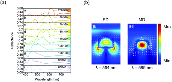
The numerically calculated reflection spectra in the visible range with varying diameters (d)/periods (p1) of Si nanodisks are shown in Fig. 2(a). With the reduction of d and p1, the reflection peak exhibits a blue-shifted resonance continuously, basically covering the entire visible region. This is due to the electric dipole (ED) and magnetic dipole (MD) modes of Mie resonance excited inside the nanodisks, which is discussed further in the next section. Upon changing the geometric parameters of nanostructures, the Mie resonance wavelengths shift, resulting in the shift of the reflection peak. The produced colors of the nanodisk arrays also change accordingly, as shown in the insets of panels a–i, including orange, green, blue, etc. The maximal reflectance can reach as high as 83% for the sample with d = 200 nm and p1 = 370 nm. While the reflectance tends to decrease in the blue and violet bands which is attributed to the relatively higher loss of Si that will produce a strong absorption effect in these wavebands,35 it remains larger than 54%.To get a better understanding of the mechanism of the resonance for the nanodisk arrays, electric and magnetic field distributions at resonance wavelengths of 564 nm and 589 nm are analyzed for one selected sample with d = 180 nm and p1 = 320 nm in the x–z cross section. As shown in Fig. 2(b), the electric field profile in the left panel depicts the excitation of an electric dipole (ED) resonance, corresponding to opposite charges accumulating at the sides of nanodisk on the Si/SiO2 interface. There is no circulation with the electric field which is oriented along the polarization of the incident electric field to a large extent. At the same time, the magnetic field distribution shown in the right panel clearly indicates a magnetic dipole (MD) resonance with an enhanced magnetic field concentrated within the nanodisk. The plotted white arrows depict the circular electric field around the nanodisk, which indicates that the MD resonance is caused by the displacement current loop.36,37 In other words, the Si nanodisks act as the Mie resonators, leading to strong optical reflection for incident light at certain wavelengths via the excitation of ED and MD modes, and they are responsible for giving rise to the colors of the SMM.
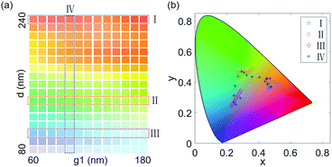
The effects of varying geometrical parameters for the disk arrays on the produced visible colors are further investigated. The simulated color palette is presented in Fig. 3(a), where the nanodisk diameters (d) vary from 80 to 240 nm from bottom to top, and the gaps (g1) between the adjacent nanodisks are changed from 60 to 180 nm from left to right, both in increments of 10 nm. Each area presents an individual color, corresponding to an array of nanodisks with a specific d and g1. As a result, a variety of vivid colors are realized including purple, blue, cyan, green, yellow, orange and red as well, covering almost the entire visible spectrum. It is observed that the increase in diameter results in a color change from purple to red in contrast to the slight color shift with the gaps increasing. This indicates that the optical response mainly depends on the radius of the nanodisk, while the internanodisk spacing hardly affects the frequency of resonances owing to the negligible effect of near-field couplings on the structural colors.38 On the basis of the calculated reflectance spectra of Si nanodisk arrays, the corresponding CIE 1931 chromaticity diagram is shown in Fig. 3(b) with discrete points extracted from the color palette. The black crosses represent the quasi-full-visible color achieved by increasing the diameter of Si nanodisks with constant gap size. Besides, royal blue stars, orange diamonds and magenta circles show three primary colors belonging to the Red–Green–Blue (RGB) color model and their small changes with the varying gap between neighboring nanodisks, which is in agreement with our analysis above.
3.2. Resonant performance in the THz range
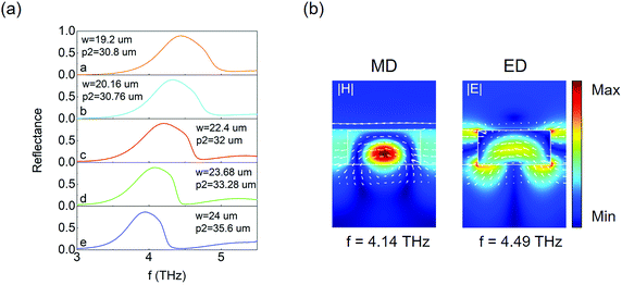
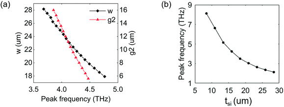
After confirming the reflection characteristics of the proposed SMM in the visible range, its THz resonance properties are investigated in detail. The THz reflection spectra at 3–5.5 THz are shown in Fig. 4(a), in which the legends denote the widths (w) and the periods (p2) of the unit cells. The trend is a monolithic red-shift of the resonance frequency with increasing w and p2, whilst still retaining high reflectance greater than 86%. For the red solid line plotted in panel c of Fig. 4(a) with d = 24 μm and p2 = 32 μm, the magnetic and electric field profiles at 4.14 and 4.49 THz are presented in Fig. 4(b). It can be seen that the reflection responses in the THz region originate from the similar Mie resonances with that of the optical band and simultaneously support ED and MD resonances. The MD resonance results from the displacement current loop which is characterized by the electric field circulating around the unit cell, as marked by the white arrows. In the right panel of Fig. 4(b), the displacement current is oriented almost in the direction of the incident electric field, resulting in the excitation of the ED resonance.39Furthermore, in order to investigate the frequency tunability of the designed SMM in the THz region, simulations with various unit cell widths (w) and intercell gaps (g2) are performed. It can be seen from Fig. 5(a) that the peak frequency gets red-shifted from 4.76 to 3.68 THz as w is increased from 17.92 to 28.16 μm. Similarly, when the gap g2 varies from 5.6 to 16 μm, the resonant peak shifts toward lower frequencies from 4.47 to 3.85 THz. One more message is contained in Fig. 5(a) that the frequency shift caused by the variation of d is approximately doubled compared to that associated with g2, indicating that the contribution of d is more significant than g2 to the THz resonant response, which is consistent with the result of the visible region. More importantly, by varying the thickness of the Si layer (tSi), which is equivalent to changing the height of the unit cell, as well as adjusting w and g2 accordingly, the THz resonant frequency can be tuned to a much greater extent. In Fig. 5(b), the reflection peak frequency could be modulated widely from 8.12 to 2.13 THz by increasing tSi from 8.4 to 28.4 μm with high reflectance efficiency larger than 78% and the maximum reflectance can reach 94%.
3.3. Independence of resonant frequency tuning in both ranges
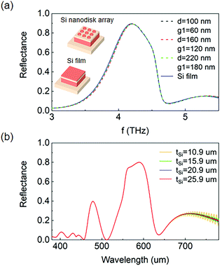
When adjusting the resonant frequencies of the SMM in the visible and THz ranges via varying geometrical parameters, it is also necessary to determine how the changes affect the spectral responses of each other. To do so a series of simulations in the THz regime are first performed on microscale unit cells with different top layers, which include the cases of the Si nanodisk array and the complete Si film, where the width (w) and period (p2) are set to 22.4 μm and 32 μm respectively. For the case of the Si nanodisk array, three samples with different d and g1 are selected and the calculated reflection spectra are shown as the dashed lines in Fig. 6(a). It is observed that the resonant frequency response for the three samples closely resembles each other, indicating that the reflection properties in THz region are not dependent on d and g1 of Si nanodisks. This is further supported through the simulation repeated by replacing the Si nanodisk array with a complete Si film of the same thickness. As depicted by the solid line in Fig. 6(a), the obtained reflection spectrum almost coincides with that of nanodisk arrays. It is therefore reasonable to describe the Si nanodisk array at terahertz frequency as a complete Si film of the same thickness without patterns,40 which means that the reflection spectra in the visible range and corresponding colors can be tuned easily by varying the diameter d and the gap g1, while this variation does not affect the THz resonance. This allows the color to be specifically arranged in each microscale unit cell, achieving flexible control over the surface color of the SMM.Then, another aspect is analyzed regarding how the regulation of resonant frequency in the THz region influences the visible performances of SMM. As illustrated in Fig. 6(b), the effect of different thicknesses of Si layer tSi on the resonance behaviour in the visible range is explored through simulations on Si nanodisk arrays with various tSi of 10.9, 15.9, 20.9 and 25.9 μm, exploiting the nanodisk parameters of d = 180 nm and p1 = 320 nm. The resulted reflection spectra exhibit identical characteristics with a negligible difference regardless of the thickness of Si layer as desired, confirming that the proposed design has a large degree of freedom to control the resonant frequency in THz regions while keeping the reflection spectra and displayed colors of Si nanodisk arrays almost constant.
4. Conclusions
In summary, an all-dielectric SMM that operates simultaneously in both the visible and terahertz frequencies is theoretically demonstrated by incorporating Si nanodisk arrays into THz unit cells on the microscale. The presented electromagnetic field distributions at reflection peaks reveal a similar Mie resonance in both regions with the excitation of ED and MD modes. In addition, it is confirmed that the independent tuning of the resonant response in both regimes can be realized with high reflectance efficiency. The simulation results indicate that the resonant wavelength in the visible regime of the SMM can be altered by varying the diameters and gaps of nanodisks, producing various colors from red to purple with maximal reflectance up to 83%, while its peak frequency in the terahertz regime can be widely modulated from 8.12 to 2.13 THz with maximum reflectance as high as 94% by changing the widths and gaps of unit cells as well as the thickness of Si layer. Since the resonances in the visible and THz bands are determined by different geometrical parameters, the variation in both regions has a negligible effect on the reflection characteristic with respect to each other. Our design opens up the prospect for a variety of applications including bio/chemical sensing, multi-spectral imaging, filtering, detection and modulation and can also satisfy people's aesthetic or functional requirements for object surface colors.Author contributions
Yeqing Zhu: conceptualization, methodology, investigation, writing – original draft. Xi Tian, Jiukai Fang: formal analysis, writing – review & editing. Yanpeng Shi: supervision, project administration, funding acquisition, validation. Shengnan Shi, Shan Zhang: data curation, formal analysis. Jinmei Song, Meiping Li, Xiaoyu Liu: visualization, writing – review & editing. Xiaodong Wang, Fuhua Yang: software, resources.Conflicts of interest
There are no conflicts to declare.Acknowledgements
This work was sponsored by the National Natural Science Foundation of China (No. 61805127), the Natural Science Foundation of Shandong Province, China (No. ZR2019BF014), the China Postdoctoral Science Foundation funded project (No. 2015M582073), the Postdoctoral Innovation Program of Shandong Province (No. 201602017) and the Fundamental Research Funds of Shandong University (No. 2018TB002).Notes and references
- V. M. Shalaev, Nat. Photonics, 2007, 1, 41–48 CrossRef CAS.
- N. I. Zheludev and Y. S. Kivshar, Nat. Mater., 2012, 11, 917–924 CrossRef CAS PubMed.
- H. M. Li, S. B. Liu, S. Y. Wang, S. Y. Liu, Y. Hu and H. B. Li, Sci. Rep., 2016, 6, 1–8 CrossRef PubMed.
- Y. Wang, Y. Leng, L. Wang, L. Dong, S. Liu, J. Wang and Y. Sun, Appl. Phys. Express, 2018, 11, 062001 CrossRef.
- N. Landy and D. R. Smith, Nat. Mater., 2013, 12, 25–28 CrossRef CAS PubMed.
- Y. Kim, T. Deng, W. X. Jiang, T. J. Cui, Y. Lee and C. W. Qiu, Phys. Rev. Appl., 2018, 10, 044027 CrossRef CAS.
- M. Ghasemi, M. Baqir and P. Choudhury, IEEE Photonics Technol. Lett., 2016, 28, 1100–1103 Search PubMed.
- W. Yang and Y. S. Lin, Opt. Express, 2020, 28, 17620–17629 CrossRef PubMed.
- H. Liu, Z. H. Wang, L. Li, Y. X. Fan and Z. Y. Tao, Sci. Rep., 2019, 9, 1–10 CrossRef PubMed.
- Z. Bao, Y. Tang, Z. D. Hu, C. Zhang, A. Balmakou, S. Khakhomov, I. Semchenko and J. Wang, Nanomaterials, 2020, 10, 1102 CrossRef CAS PubMed.
- F. Li, H. Chen, Q. He, Y. Zhou, L. Zhang, X. Weng, H. Lu, J. Xie and L. Deng, J. Opt., 2019, 21, 045102 CrossRef CAS.
- A. Keshavarz and A. Zakery, Plasmonics, 2018, 13, 459–466 CrossRef CAS.
- P. C. Abad, J. Y. Ou, E. Plum and N. I. Zheludev, Sci. Rep., 2017, 7, 1–7 CrossRef PubMed.
- A. L. Chan and S. R. Schnelle, Opt. Eng., 2013, 52, 017004 CrossRef.
- I. J. H. McCrindle, J. P. Grant, L. C. P. Gouveia and D. R. S. Cumming, Phys. Status Solidi A, 2015, 212, 1625–1633 CrossRef CAS.
- A. V. Kabashin, P. Evans, S. Pastkovsky, W. Hendren, G. A. Wurtz, R. Atkinson, R. Pollard, V. A. Podolskiy and A. V. Zayats, Nat. Mater., 2009, 8, 867–871 CrossRef CAS PubMed.
- C. Zhang, L. Liang, L. Ding, B. Jin, Y. Hou, C. Li, L. Jiang, W. Liu, W. Hu and Y. Lu, Appl. Phys. Lett., 2016, 108, 241105 CrossRef.
- X. Chen and W. Fan, Sci. Rep., 2017, 7, 1–8 CrossRef PubMed.
- J. Zhong, X. Xu and Y. S. Lin, Nanomaterials, 2021, 11, 2175 CrossRef CAS PubMed.
- Y. Zhang, T. Li, B. Zeng, H. Zhang, H. Lv, X. Huang, W. Zhang and A. K. Azad, Nanoscale, 2015, 7, 12682–12688 RSC.
- C. Wu, A. B. Khanikaev, R. Adato, N. Arju, A. A. Yanik, H. Altug and G. Shvets, Nat. Mater., 2012, 11, 69–75 CrossRef CAS PubMed.
- Y. Li, B. An, S. Jiang, J. Gao, Y. Chen and S. Pan, Opt. Express, 2015, 23, 17607–17612 CrossRef CAS PubMed.
- Y. Bai, Y. Jiang and L. Liu, J. Phys. D: Appl. Phys., 2014, 47, 445304 CrossRef.
- A. Ahmadi and H. Mosallaei, Phys. Rev. B: Condens. Matter Mater. Phys., 2008, 77, 045104 CrossRef.
- S. J. Corbitt, M. Francoeur and B. Raeymaekers, J. Quant. Spectrosc. Radiat. Transfer, 2015, 158, 3–16 CrossRef CAS.
- J. Grant, I. J. McCrindle and D. R. Cumming, Opt. Express, 2016, 24, 3451–3463 CrossRef CAS PubMed.
- S. Gao, C. S. Park, S. S. Lee and D. Y. Choi, Nanoscale, 2019, 11, 4083–4090 RSC.
- L. Yang, D. Wu, Y. Liu, C. Liu, Z. Xu, H. Li, Z. Yu, L. Yu and H. Ye, Photonics Res., 2018, 6, 517–524 CrossRef CAS.
- S. Jahani and Z. Jacob, Nat. Nanotechnol., 2016, 11, 23–36 CrossRef CAS PubMed.
- P. Moitra, B. A. Slovick, W. Li, I. I. Kravchencko, D. P. Briggs, S. Krishnamurthy and J. Valentine, ACS Photonics, 2015, 2, 692–698 CrossRef CAS.
- S. Manjunath, M. Liu, V. Raj, R. A. Aoni, D. A. Powell, I. V. Shadrivov and M. Rahmani, Adv. Opt. Mater., 2020, 8, 1901658 CrossRef CAS.
- W. Li, Y. Shi, Z. Chen and S. Fan, Nat. Commun., 2018, 9, 1–8 CrossRef PubMed.
- S. Li, K. Liu, X. Long, L. Chen, Z. Xie, L. Li and X. Zhou, Opt. Commun., 2020, 459, 124950 CrossRef CAS.
- S. Westland, C. Ripamonti and V. Cheung, Chapter 4 -Computing CIE tristimulus values, in Computational Colour Science Using MATLAB, ed. M. A. Kriss, Wiley, Hoboken, 2nd edn, 2012, pp. 27–47 Search PubMed.
- X. Huang, J. Huang, L. Yang, Z. Zhang, H. Ma, Y. Qian, C. Li, Z. Zhang and J. Yang, IEEE Photonics J., 2021, 13, 1–9 Search PubMed.
- G. W. Castellanos, P. Bai and J. Gómez Rivas, J. Appl. Phys., 2019, 125, 213105 CrossRef.
- W. Yue, S. Gao, S. S. Lee, E. S. Kim and D. Y. Choi, Laser Photonics Rev., 2017, 11, 1600285 CrossRef.
- L. Li, J. Niu, X. Shang, S. Chen, C. Lu, Y. Zhang and L. Shi, ACS Appl. Mater. Interfaces, 2021, 13, 4364–4373 CrossRef CAS PubMed.
- Z. Ma, S. M. Hanham, P. Albella, B. Ng, H. T. Lu, Y. Gong, S. A. Maier and M. Hong, ACS Photonics, 2016, 3, 1010–1018 CrossRef CAS.
- I. J. McCrindle, J. Grant, T. D. Drysdale and D. R. Cumming, Opt. Express, 2013, 21, 19142–19152 CrossRef CAS PubMed.
| This journal is © The Royal Society of Chemistry 2022 |

