
 Open Access Article
 This Open Access Article is licensed under a Creative Commons Attribution-Non Commercial 3.0 Unported Licence
Electroforming-free threshold switching of NbOx–based selector devices by controlling conducting phases in the NbOx layer for the application to crossbar array architectures
Kitae Park a,
Jiyeon Ryua,
Dwipak Prasad Sahub,
Hyun-Mi Kimc and
Tae-Sik Yoon*ab
a,
Jiyeon Ryua,
Dwipak Prasad Sahub,
Hyun-Mi Kimc and
Tae-Sik Yoon*ab
aGraduate School of Semiconductor Materials and Devices Engineering, Ulsan National Institute of Science and Technology, Ulsan 44919, Republic of Korea. E-mail: tsyoon@unist.ac.kr
bDepartment of Materials Science and Engineering, Ulsan National Institute of Science and Technology, Ulsan 44919, Republic of Korea
cKorea Electronics Technology Institute, Gyeonggi-do 13509, Republic of Korea
First published on 23rd June 2022
Abstract
Bipolar threshold switching characteristics, featuring volatile transition between the high-resistance state (HRS) at lower voltage than threshold voltage (Vth) and the low-resistance state (LRS) at higher voltage irrespective of the voltage polarity, are investigated in the Nb(O)/NbOx/Nb(O) devices with respect to deposition and post-annealing conditions of NbOx layers. The device with NbOx deposited by reactive sputtering with 12% of O2 gas mixed in Ar shows threshold switching behaviors after electroforming operation at around +4 V of forming voltage (Vf). On the other hand, electroforming-free threshold switching is achieved from the device with NbOx deposited in the reduced fraction of 7% of O2 gas and subsequently annealed at 250 °C in vacuum, thanks to the increase of the amount of conducting phases within the NbOx layer. Threshold switching is thought to be driven by the formation of a temporally percolated filament composed of conducting NbO and NbO2 phases in the NbOx layer, which were formed as a result of the interaction with Nb electrodes such as oxygen ion migration either by annealing or electrical biasing. The presence of a substantial amount of oxygen in the Nb electrodes up to ∼40 at%, named Nb(O) herein, would alleviate excessive migration of oxygen and consequent overgrowth of the filament during operation, thus enabling reliable threshold switching. These results demonstrate a viable route to realize electroforming-free threshold switching in the Nb(O)/NbOx/Nb(O) devices by controlling the contents of conducting phases in the NbOx layer for the application to selector devices in high-density crossbar memory and synapse array architectures.
1. Introduction
In order to fabricate high-density two-terminal resistive random access memory (RRAM) and artificial synapses, crossbar array architectures have been employed for the benefit of their 4F2 cell sizes (F is the minimal feature size).1 In the crossbar array architectures, it is essential to minimize unintended leakage current through neighboring unselected cells, called sneak path leakage current, to avoid erroneous operation as well as to reduce operation power.2–4 Various approaches have been pursued to minimize sneak path leakage current by integrating additional selector devices such as transistors,5 diodes,6 tunnel barriers,7 mixed ionic electronic conduction (MIEC) devices8,9 having highly non-linear current–voltage characteristics, and threshold switching selectors having abrupt switching between insulating and conducting states.10–16 Among these, the use of two-terminal selectors has advantages of high scalability due to small feature size and the same two-terminal structure with memory or a synapse cell that enables it to be directly integrated by stacking devices.As two-terminal selectors, the threshold switching selectors feature to have an abrupt increase of current when the applied voltage exceeds a threshold voltage (Vth), resulting in switching operation. They have a reversible and volatile change of resistance between a high-resistance state (HRS) at a lower voltage than Vth and a low-resistance state (LRS) at a higher voltage than Vth, which is analogous to resistance change in non-volatile RRAM cells except that the resistance change is volatile in nature upon removing applied voltage due to temporary formation of the conducting filament.16–20 The analogous nature of threshold switching selectors and RRAM cells enables them to be readily integrated and operated by tuning the conditions to obtain volatile unstable filament formation in threshold switching selectors and non-volatile stable filament formation in RRAM cells.
One route to realize threshold switching selectors is the use of diffusive memristors operated by temporal and diffusive dynamics of filament evolution consisting of active metal species such as Ag and Cu in electrolyte oxide layers.17,21,22 The filament is formed by electrochemical metallization for temporary switching from HRS to LRS only while the voltage higher than Vth is applied, and it is spontaneously dissolved after removing the applied voltage. Another route is to form the temporary filament composed of oxygen vacancies, corresponding to valence change memory (VCM)-type RRAM.23–25 In this device, oxygen ions migrate from the resistive switching oxide layer to oxygen-reactive electrode, then oxygen vacancies in the oxide layer coalesce and form a conducting filament. In contrast to VCM-type RRAM, the filament is unstable and suddenly dissociated when the applied voltage is removed, thereby leading to volatile threshold switching.
In this study, the VCM-type threshold switching characteristics particularly with electroforming-free (also called “forming-free”) operations were demonstrated with a simple metal-insulator-metal (MIM) structure of Nb/NbOx/Nb, where niobium (Nb) and niobium oxide (NbOx) play the role of oxygen-reactive electrode and resistive switching layer, respectively. To date, NbOx has been examined as promising selector material with the structures such as W/NbOx/TiN,14 Pt/NbOx/Pt,15 Pt/NbO2/Nb2O5/Pt,12 and Ti/NbOx/Ti.26 However, most of the devices generally require the forming operation to obtain consequent threshold switching characteristics. Distinct from those previous reports, in this study, Nb was used as oxygen-reactive electrodes for the threshold switching of NbOx switching layer, particularly for the forming-free threshold switching. In addition, it is expected to have reliable interfaces and to simplify fabrication procedures for reduced processing budget and increased production yield by using Nb electrodes for NbOx switching layer. Electroforming-free threshold switching could be achieved by controlling deposition conditions and employing the post-deposition annealing process of NbOx layer to obtain proper contents of conducting NbO and NbO2 phases mixed with insulating Nb2O5 phase.
2. Experimental
The threshold switching devices were prepared with the structure of Nb(O)/NbOx/Nb(O) as follows. A 70 nm-thick Pt with a 30 nm-thick Ti adhesion layer was deposited on SiO2/Si substrate by e-beam evaporation under the base pressure lower than 10−6 Torr. Then, a 90 nm-thick Nb(O) bottom electrode (BE) was deposited by direct-current (dc) magnetron sputtering with a 99.995% pure Nb target in a diameter of 2 inches at room temperature in an Ar ambient. The base pressure was in the range of 10−6 Torr and a working pressure was 10 mTorr. Its deposition rate was 9 nm min−1. Although the electrode was deposited in an Ar ambient, it was deposited as the mixture mostly of Nb and NbO phases with oxygen content of almost 40 at%, as discussed layer. Therefore, the electrodes are presented herein as Nb(O). A 90 nm-thick NbOx resistive switching layer was subsequently deposited by dc magnetron reactive sputtering using the same Nb target in 7% or 12% O2 gas mixed in Ar, which is named hereafter 7%-device and 12%-device with these switching layers, respectively. The deposition rates of 7% and 12% NbOx layers were 14.3 and 16.7 nm min−1, respectively. The other conditions for the deposition were maintained to be same for each other. A Nb(O) top electrode (TE) with a diameter of 100 μm was finally deposited using a shadow mask. In addition, the device with NbOx deposited in 7% O2 gas and subsequently annealed at 250 °C in the deposition chamber at a pressure in the range of 10−4 Torr for an hour right after deposition of Nb(O) TE was prepared as named 7% annealed-device. The threshold switching characteristics were examined using Agilent 4156B and Keithley 4200A-SCS semiconductor parameter analyzers. The voltage was applied to Nb(O) TE and the Nb(O)/Pt BE was kept grounded. The microstructures of NbOx layers and device structures were analyzed by using scanning electron microscope under acceleration voltage of 10 kV (SEM, Quanta 200FEG) and transmission electron microscope under acceleration voltage of 200 kV (TEM, ARP200P). TEM specimens were prepared by focused ion beam method with Ga ions (FIB, Helios NanoLab 450/FEI). The chemical bonding states and compositions of the layers were analyzed by using X-ray photoelectron spectroscopy (XPS, K-alpha) and Auger electron spectroscopy under acceleration voltage of 3 kV (AES, PHI-700).3. Results and discussion
Fig. 1 shows the current–voltage (I–V) sweep curves of three Nb(O)/NbOx/Nb(O) devices with respect to preparation conditions. Fig. 1(a)–(c) show the I–V sweep curves of 12%-, 7%-, and 7%-annealed devices, respectively. The voltage sweep was performed by increasing applied voltage amplitude in a linear staircase manner and the current was measured with an integration time of 0.64 ms. First, the 12%-device required forming operation by sweeping voltage 0 → +5 → 0 V as shown at the inset of Fig. 1(a). The compliance current for the forming operation was set to be 0.02 A to prevent excessive filament growth. At forming operation, the current was abruptly increased from ∼10−3 to 0.02 A at the forming voltage (Vf) of around +4 V during forward sweep of 0 → +5 V and decayed back to ∼10−3 A at +1 V during backward sweep of +5 → 0 V. In general, the forming operation is required to make either volatile or nonvolatile conducting path through insulating layers to alternatingly form and rupture filament at subsequent voltage application steps for threshold switching or memory operations, respectively. Even at forming operation, the I–V curve shows volatile threshold switching, implying that the filament formed at the forming operation is temporarily sustainable as volatile filament. As will be further discussed with Fig. 3, the resistivity of the NbOx layer at HRS (off-state) was substantially decreased by up to four orders of magnitude of the increased current level after forming operation. It implies that the layer became to have partially formed filament or abundant conducting phases or defects that provide the conducting path by the forming operation. As shown in Fig. 1(a), after forming operation, the device shows threshold switching behaviors upon alternatively repeating positive voltage sweeps 0 → +2 → 0 V and following negative voltage sweeps 0 → −2 → 0 V at the compliance current of 0.1 A. During repeated positive and negative voltage sweeps by total forty times, the threshold switching characteristics remained stable at both polarities with Vth of around ±1.2 V for an abrupt increase of current and the hold voltage (Vhold) of around ±0.9 V at which the current descended back abruptly. The HRS/LRS ratio is measured to be in the range of 30 ∼ 100 at the Vth.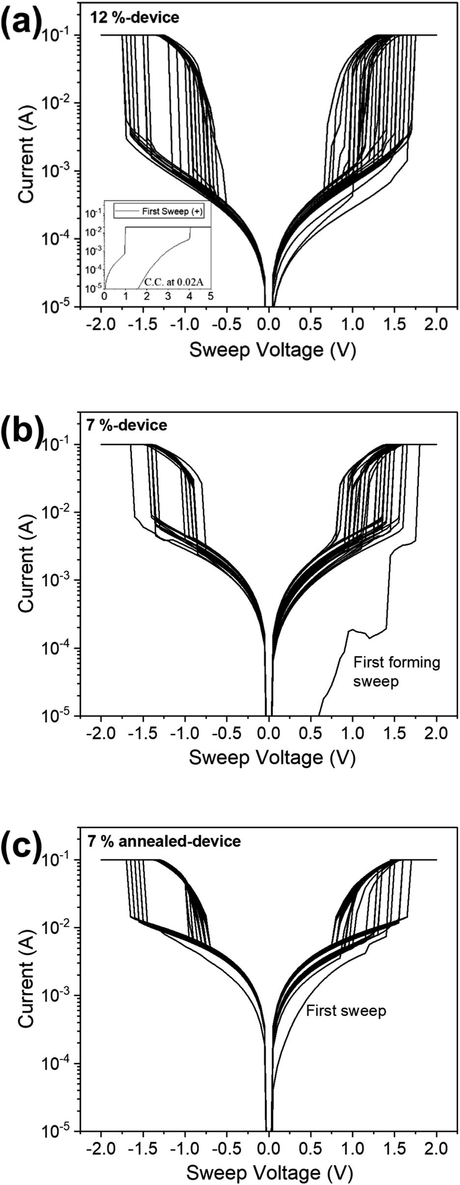 | ||
| Fig. 1 I–V sweep curves of (a) 12%-device, (b) 7%-device, and (c) 7% annealed-device. | ||
The 7%-device with reduced O2 gas mixture required also forming operation at the Vf of around +1.8 V during the first voltage sweep of 0 → +2 → 0 V at the compliance current of 0.1 A as shown in Fig. 1(b). Its compliance current for the forming operation was set to be higher than that of the 12%-device because of the higher conductivity of the NbOx layer in the 7%-device. The Vf of about +1.8 V in the 7%-device is much smaller than around +4 V in the 12%-device because the NbOx layer in the 7%-device is initially more conducting with a higher content of conducting phases, as confirmed from XPS analysis (Fig. 11), to readily form the filament. After the first sweep, the device shows threshold switching with Vth of around ±1.2 V and Vhold of around ±0.9 V during repeated 0 → ±2 → 0 V sweeps. It is noted that the HRS/LRS ratio ranges from 10 to 20, which is smaller than that of the 12%-device due to higher conductivity of the NbOx layer at the HRS in the 7%-device.
Compared to these devices, the I–V curves of the 7% annealed-device in Fig. 1(c) show notable feature of forming-free threshold switching. The threshold switching is observed even at the first sweep curve of 0 → +2 → 0 V as to be almost identical to those in the following sweeps. Except for the forming-free operation, other properties such as the values of Vth, Vhold, and the HRS/LRS ratio are nearly the same with those of the 7%-device shown in Fig. 1(b). The forming-free operation in the 7% annealed-device comes from the interaction between Nb(O) electrodes and NbOx switching layer such as oxygen migration during the post-annealing at 250 °C. The interaction such as oxygen migration depletes oxygen from the NbOx layer to increase the content of conducting NbO and NbO2 phases, as confirmed with XPS analysis in Fig. 11. As schematically illustrated in Fig. 2, the post-annealing drives oxygen atoms to the Nb(O) electrode and increases the concentration of oxygen vacancies in the NbOx layer (Fig. 2(a) and (b)), and these vacancies form the volatile filament as being aligned under the electric field (Fig. 2(c)). It verifies that the post-annealing to migrate oxygen atoms to electrodes and subsequent increase of oxygen vacancy concentration (content of conducting phases) could be a simple and viable route of forming operation alternative to electric biasing. The mechanism of threshold switching is further discussed later with the results of structure, composition, and bonding state analyses.
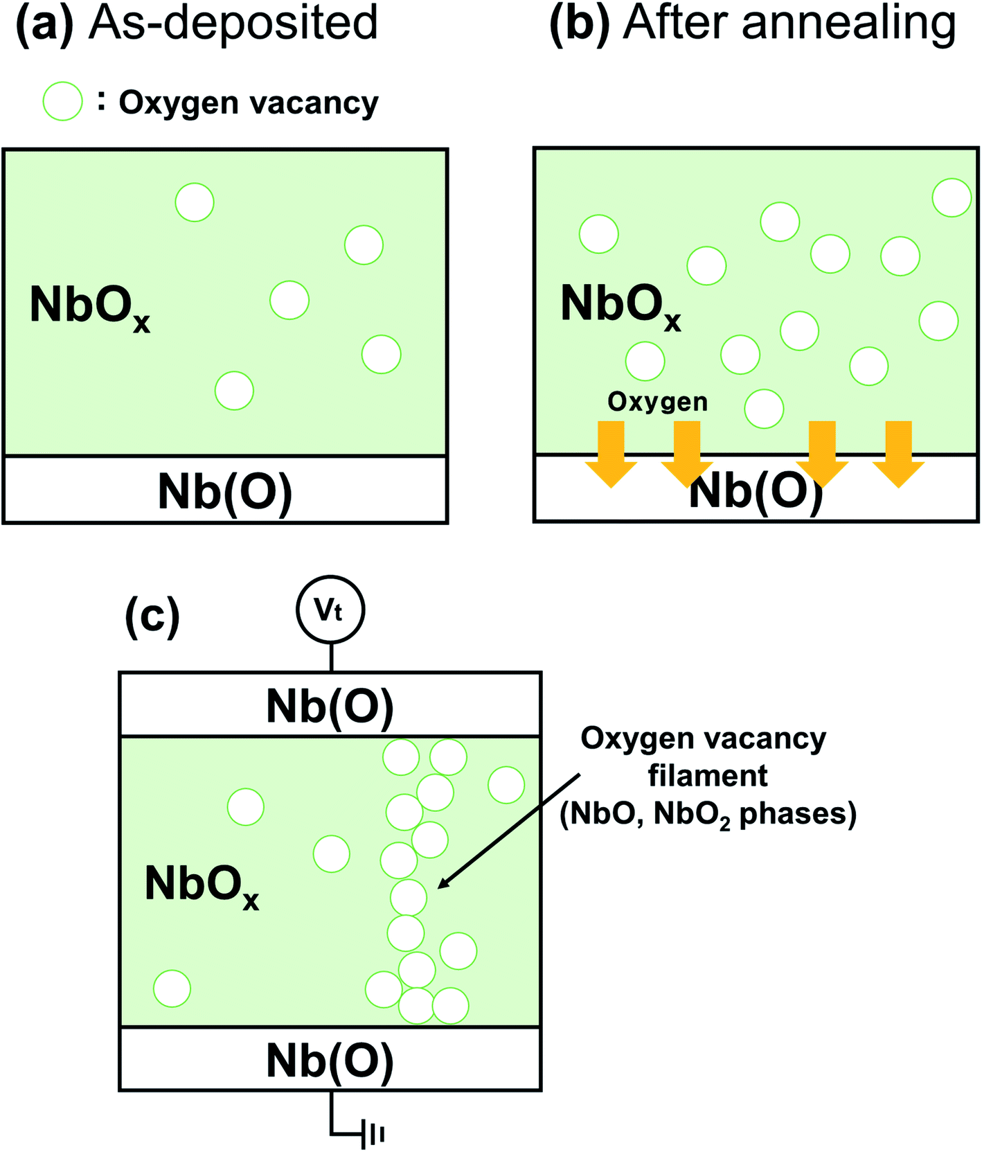 | ||
| Fig. 2 Schematic illustration of forming-free threshold switching mechanism in the 7% annealed-device associated with the increased oxygen vacancy formation by annealing and the field-induced alignment of vacancies for filament formation: (a) as-deposited state, (b) after annealing to increase oxygen vacancy concentration, i.e., increase of NbO and NbO2 phases, and (c) alignment of vacancies for temporary formation of conducting filament. | ||
Fig. 3(a)–(c) show the I–V curves of randomly chosen seven different cells at the first two voltage sweeps of the 12%-, 7%-, and 7% annealed-devices, respectively, to examine the forming characteristics. In the 12%-device, as shown in Fig. 3(a), the forming took place at around ±4 V of the first sweep. The HRS current before forming was about 10−7 A at +1 V, which was the lowest among those of the three devices. Then, it was increased to the range of 10−4 A at following sweep, and Vth was around +1 V. The measured seven devices showed a narrow distribution of switching parameters such as the currents at HRS and LRS, the values of Vf and Vth. The I–V curves of the 7%-device are found to be rather dispersed at the first sweep for the forming operation with deviated Vf values and multiple current changes. Then, threshold switching behaviors are stabilized at the second sweep. The I–V sweeps of the 7% annealed-device show the forming-free and uniform threshold switching characteristics, where the curves at the first and the second sweeps are almost same with a little higher Vth of +1.5 ∼ +2.0 V at the first sweep than about +1 V at the second sweep.
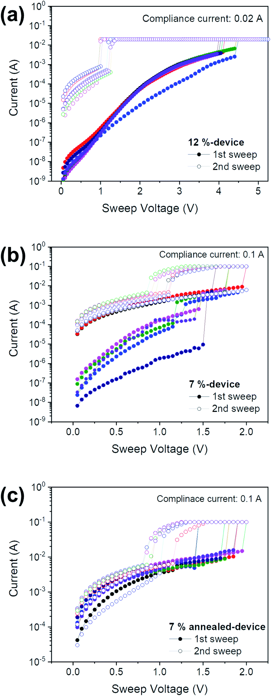 | ||
| Fig. 3 I–V curves of randomly chosen seven different cells at the first two voltage sweeps of (a) 12%-, (b) 7%-, and (c) 7% annealed-devices. | ||
Fig. 4 compares current levels at HRS and LRS of the 12%-, 7%-, and 7% annealed-devices when the voltage sweeps for the threshold switching operations were repeated eighty times to assess endurance properties. The currents values right before and after threshold switching at Vth are presented for those of HRS and LRS, respectively. As shown in Fig. 4(a), the 12%-device has a lowest HRS current of ∼5 × 10⁻⁴ A due to its lowest conductivity of the NbOx layer, resulting in the highest HRS/LRS ratio of ∼200. However, the device experienced a hard breakdown as being stuck to LRS after repeating forty times of voltage sweeps possibly due to the overgrowth of filament. The gradual increase of current manifests continued growth of filament during the repetition of sweeps. On the other hand, both the 7%- and 7%-annealed devices exhibit the reliable threshold switching up to eighty times of operations, although there is a trade-off with the smaller HRS/LRS ratio of around 10 ∼ 30 due to their higher HRS currents in the range of 10−3 A.
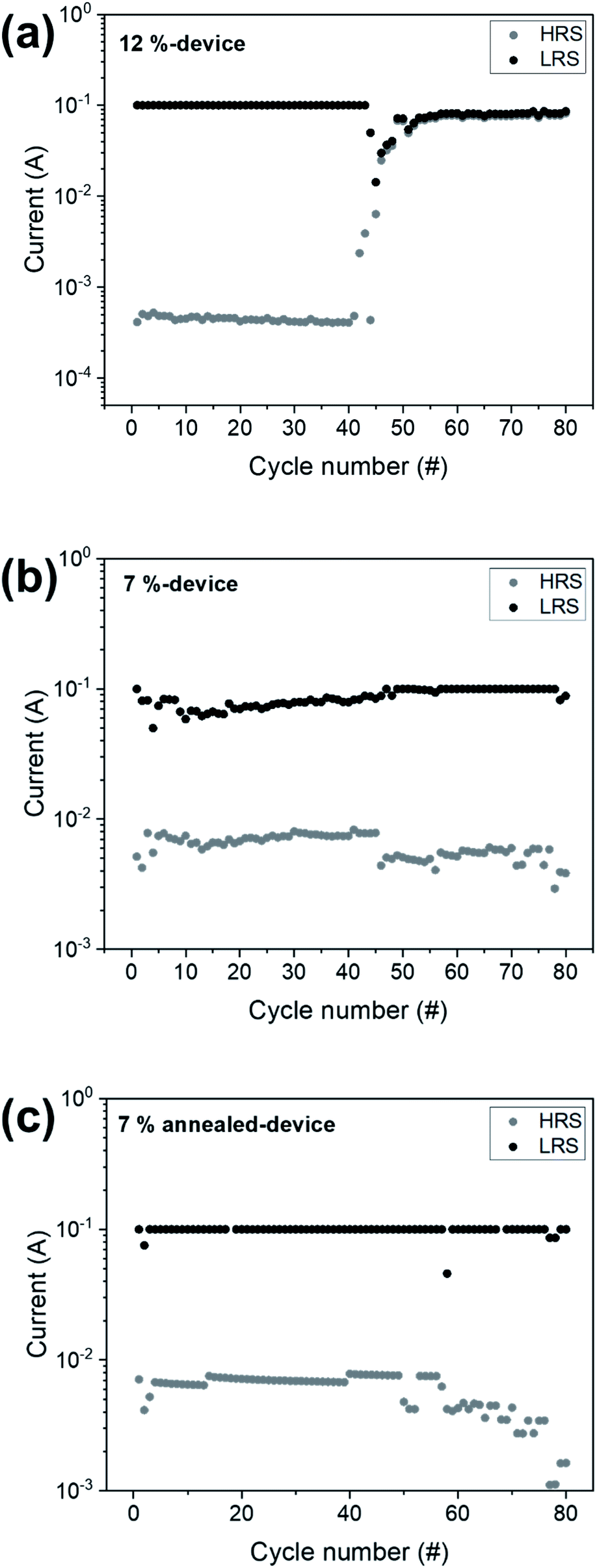 | ||
| Fig. 4 Current levels at HRS and LRS of (a) 12%-, (b) 7%-, and (c) 7% annealed-devices as repeating threshold switching operations eighty times. | ||
The uniformity of threshold switching characteristics was evaluated with cycle-to-cycle and cell-to-cell variations of Vth and Vhold values. Fig. 5 presents cycle-to-cycle distribution of Vth and Vhold values extracted from a hundred switching cycles as cumulative probability functions for the 12%-, 7%-, and 7% annealed-devices. It is found that all three devices have Vth and Vhold values within narrow ranges. The mean value (μ) and standard deviation (σ) of Vth of the 12%-device are 1.52 V and 0.31 V, respectively, corresponding to σ/μ ∼ 0.2, i.e., ∼20% deviation from mean value, as shown in Fig. 5(a). Also, μ and σ of Vhold are 1.23 V and 0.15 V, respectively, corresponding to ∼12% deviation. As shown in Fig. 5(b), the 7%-device has similar distributions that μ and σ of Vth are 1.24 V and 0.15 V, respectively, rendering ∼12% deviation, and μ and σ of Vhold are 0.87 V and 0.06 V, respectively, with ∼7% deviation. In addition, the 7% annealed-device has similar values that μ and σ of Vth are 1.42 V and 0.11 V, respectively, rendering ∼8% deviation, and μ and σ of Vhold are 0.81 V and 0.07 V, respectively, with ∼9% deviation (Fig. 5(c)).
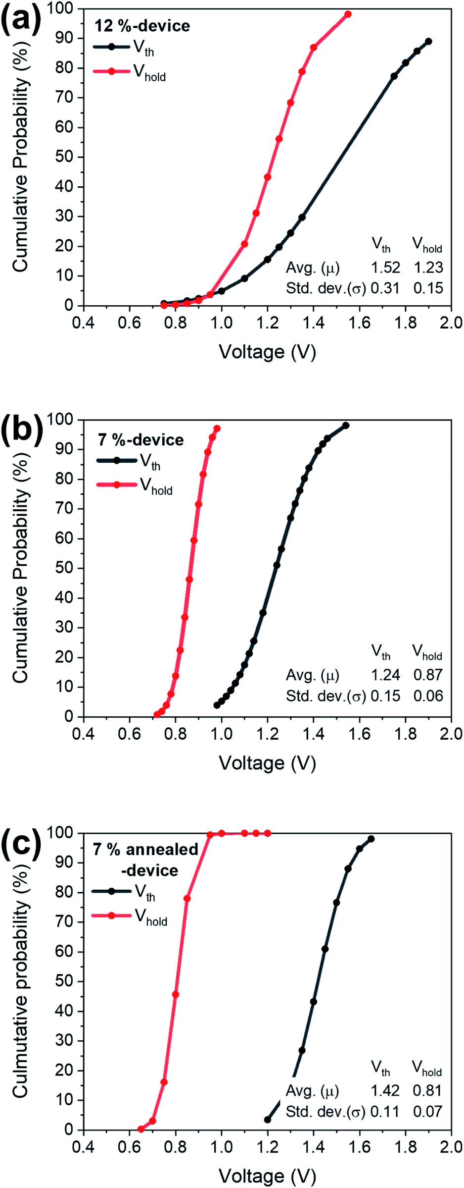 | ||
| Fig. 5 Cycle-to-cycle distribution of Vth and Vhold values extracted from a hundred cycles by cumulative probability functions for (a) 12%-, (b) 7%-, and (c) 7% annealed-devices. | ||
Fig. 6 shows the cell-to-cell variation of Vth values obtained at positive and negative voltage sweeps of randomly selected cells of the 12%-, 7%-, and 7% annealed-devices. The sets of positive voltage sweeps repeated five time and following negative voltage sweeps five times were repeated consecutively. The Vth values at both the positive and negative sweeps are found to be within narrow ranges marked as cyan color bands. These results indicate good threshold switching uniformity with a narrow distribution of switching parameters, irrespective of the NbOx preparation conditions. Considering a half-bias operation scheme in crossbar array architectures, where the selected cell is full-biased while unselected cells are half-biased,27 it is important to achieve the conditions for on-state (LRS) at “±V” and off-state (HRS) at “±V/2” simultaneously. Although the measured Vth values are little scattered from cell to cell, it is found that the values of ±Vth/2 for the off-state are mostly out of the ±Vth ranges for the on-state thanks to the narrow Vth distribution, satisfying the requirement of half-bias scheme.
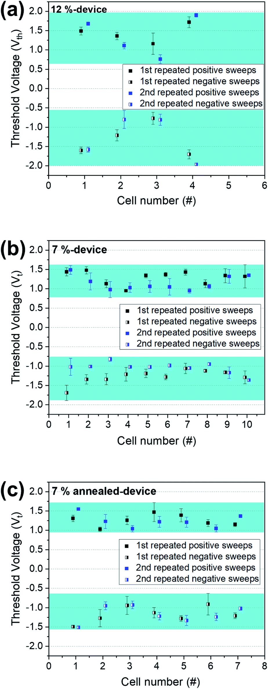 | ||
| Fig. 6 Cell-to-cell variation of Vth values obtained at positive and negative voltage sweeps of randomly selected cells of (a) 12%-, (b) 7%-, and (c) 7% annealed-devices. | ||
The comparison of threshold switching characteristics of three devices demonstrates that all devices have threshold switching behaviors for the application to selector devices while the switching parameters such as Vf, Vth, Vhold, HRS/LRS ratio, and endurance properties are determined by the preparation conditions of the NbOx layers. It is also notable that the threshold switching characteristics remained stable and even further improved by post-annealing. This thermal stability of threshold switching is beneficial for the integrated device fabrication requiring the processing steps at elevated temperatures.
Fig. 7 shows the threshold switching of the 7% annealed-device in response to voltage pulse application. During +1 V pulse application with a width of 100 μs, the current remained to be low with the value of about 8 × 10⁻⁴ A which coincides with the off-state (HRS) current in I–V sweep results in Fig. 1. Then, applying +2 V pulse increases the current to 0.02 A set to be the compliance current, which is the on-state (LRS) current in the threshold switching. Fig. 7(b) is the magnified graph at the onset of the increase of current upon applying +2 V pulse marked with black square in Fig. 7(a). The abrupt increase of current to LRS occurred clearly within the response time < 100 ns, which demonstrates a fast switching behavior. From the hypothesis of threshold switching mechanism associated with alignment of oxygen vacancy as a VCM-type switching, it implies that the local alignment of oxygen vacancies to form temporary filament within NbOx layer takes place very quickly within tens of ns.
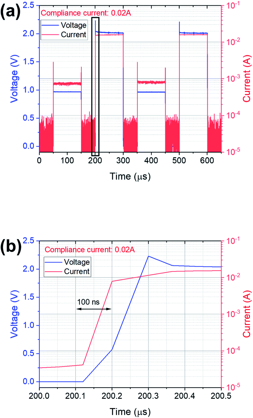 | ||
| Fig. 7 (a) Pulse measurements of the 7% annealed-device by applying +1 V for HRS and +2 V for LRS with a pulse width of 100 μs and (b) magnified graph at the onset of the increase of current upon applying +2 V pulse marked with black square in (a). | ||
Microstructures of the Nb(O)/NbOx/Nb(O) devices were also investigated using SEM and TEM analyses. Fig. 8(a) and (b) are plan-view SEM micrographs of the surface of NbOx layers deposited in 12% and 7% O2 gas, respectively. Even though the threshold switching behaviors and the current levels of the devices with these layers are distinguishable from each other, their microstructures are almost identical to have granular structures with the size in the range of 50 ∼ 100 nm. However, it should be noted that the layers are not crystalline even with granular structures as confirmed from selected area diffraction patterns (SADP) analysis in Fig. 9.
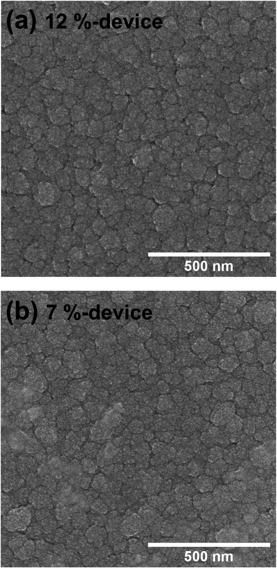 | ||
| Fig. 8 Plan-view SEM micrographs of the surface of NbOx layers deposited in (a) 12% and (b) 7% O2 gas. | ||
 | ||
| Fig. 9 (a) Bright-field and (b) high-resolution cross-sectional TEM micrographs, (c) high angle annular dark field micrograph in STEM mode, and (d) SADP of 12%-device, (e) bright-field cross-sectional TEM micrograph and (f) SADP of 7%-device. | ||
Fig. 9(a)–(d) are bright-field (BF) and high-resolution (HR) cross-sectional TEM micrographs, and high angle annular dark field (HAADF) micrograph in STEM (scanning TEM) mode, and SADP of the 12%-device, respectively. Similar to SEM micrograph, the NbOx layer is found to have columnar structure with undulating contrast within the layer, implying the presence of porous regions inside the layer.28 These porous regions would be facilitated path for the filament formation under the electric field. The HR-TEM micrograph in Fig. 9(b) and HAADF micrograph in Fig. 9(c) confirm that the NbOx layer is amorphous with locally porous regions as shown to be with undulating contrast. The Nb(O) electrodes have also the columnar structure as generally observed from polycrystalline metal layers. Its crystalline feature is also found in HAADF micrograph with white spots representing diffracted grains in Fig. 9(c), implying that their size is tens of nanometers scattered inside granular structures. The SADP analysis in Fig. 9(d) discloses also that Nb(O) electrode is polycrystalline. However, it is not a pure Nb, but includes NbO crystallites,29 due to the incorporation of oxygen atoms inside the layer as also confirmed from following AES analysis results in Fig. 10. The NbOx layer and Nb(O) electrodes in the 7%-device shown in Fig. 9(e) and (f) have almost the same microstructures and phases as those of the 12%-device, and it indicates that the difference in O2 content from 7 to 12% in the sputtering conditions does not alter the microstructures and phases of the NbOx layers significantly although the threshold switching characteristics are substantially distinguishable.
 | ||
| Fig. 10 AES depth profiles of (a) 12%- and (b) 7%-devices. | ||
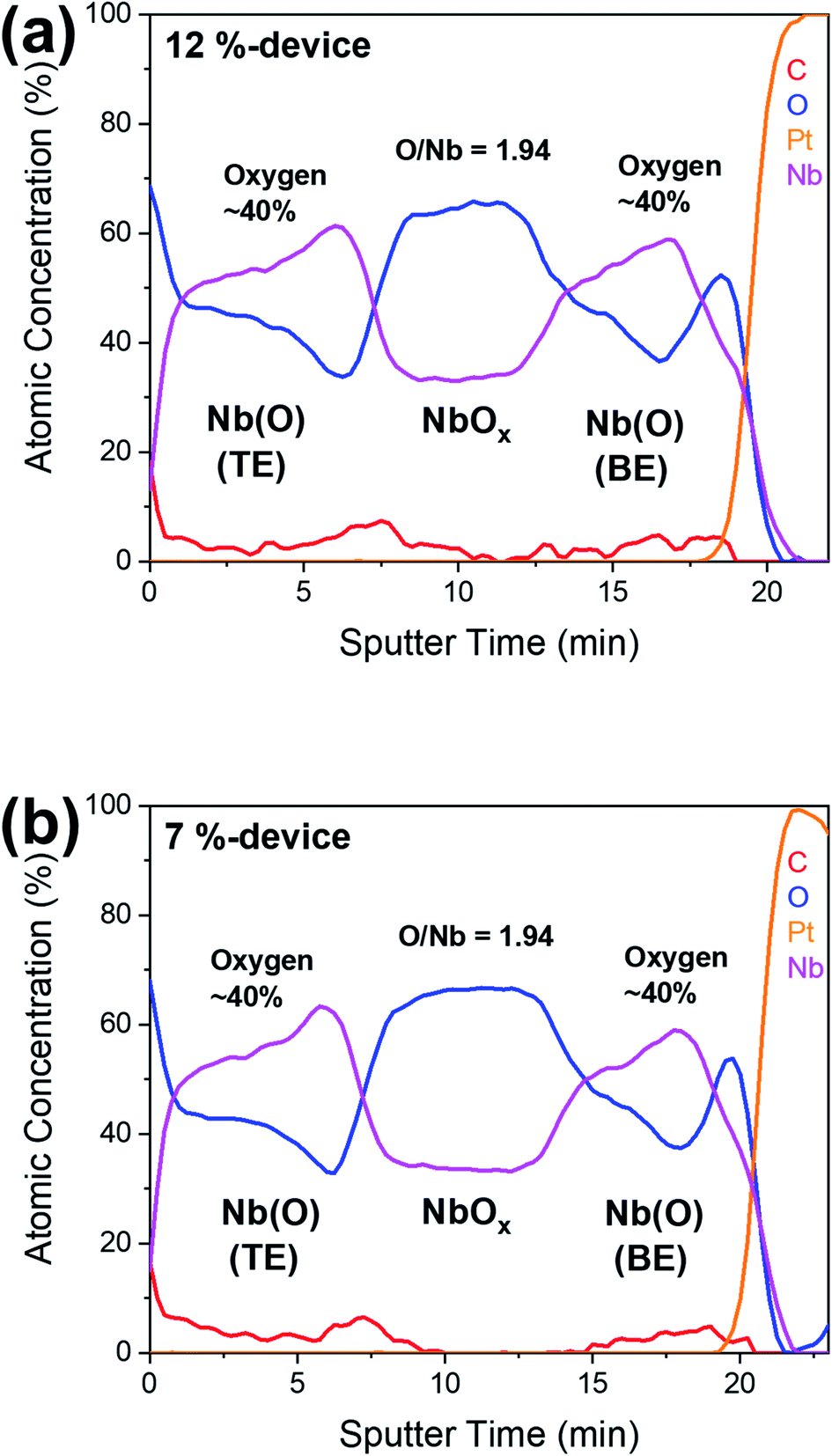
The compositional analyses were carried out in the 12%- and 7%-devices through AES depth profiling as shown in Fig. 10(a) and (b), respectively. In the NbOx layers of both devices, the approximate ratios of Nb![[thin space (1/6-em)]](https://www.rsc.org/images/entities/char_2009.gif) :O = 1:1.9 were observed regardless of the preparation conditions of NbOx layers. It implies that NbOx layers are the mixture of insulating Nb2O5 and conducting NbO2 and NbO phases.30 In addition, Nb(O) TE and BE are found to have substantial oxygen content up to almost 40 at%, resulting from the incorporation of oxygen atoms through their grain boundaries and also during their sputtering deposition.31 It is also notable that oxygen content in Nb(O) TE near top Nb(O)/NbOx interface is depleted while it is accumulated near bottom Nb(O)/NbOx interface. The decent gradient of oxygen content in the Nb(O) TE with its depletion near top interface is explained with that oxygen atoms were incorporated from top surface as the device was exposed to air. The accumulation of oxygen in the Nb(O) BE near bottom interface could result from the penetration of oxygen atoms during NbOx deposition in O2 mixed gas due to high reactivity of Nb with oxygen. Indeed, the resistivity of partially oxidized Nb(O) electrode was measured to be around 9.4 × 10⁻⁴ Ω cm using a 4-point probe (CMT 2000N, AIT), which is much higher than the reported value of 2 × 10⁻⁶ Ω cm of pure Nb layer.32
:O = 1:1.9 were observed regardless of the preparation conditions of NbOx layers. It implies that NbOx layers are the mixture of insulating Nb2O5 and conducting NbO2 and NbO phases.30 In addition, Nb(O) TE and BE are found to have substantial oxygen content up to almost 40 at%, resulting from the incorporation of oxygen atoms through their grain boundaries and also during their sputtering deposition.31 It is also notable that oxygen content in Nb(O) TE near top Nb(O)/NbOx interface is depleted while it is accumulated near bottom Nb(O)/NbOx interface. The decent gradient of oxygen content in the Nb(O) TE with its depletion near top interface is explained with that oxygen atoms were incorporated from top surface as the device was exposed to air. The accumulation of oxygen in the Nb(O) BE near bottom interface could result from the penetration of oxygen atoms during NbOx deposition in O2 mixed gas due to high reactivity of Nb with oxygen. Indeed, the resistivity of partially oxidized Nb(O) electrode was measured to be around 9.4 × 10⁻⁴ Ω cm using a 4-point probe (CMT 2000N, AIT), which is much higher than the reported value of 2 × 10⁻⁶ Ω cm of pure Nb layer.32
Fig. 11 shows Nb 3d spectra presenting chemical bonding states of Nb cations in NbOx layers analyzed by using XPS.33,34 For XPS analysis, the measurement spot size was 400 μm in diameter. The measurement was performed at the middle positions in thickness of Nb(O) TE and NbOx layers in the devices after etching with Ar gas. The peaks were calibrated with C 1s peak at 284.5 eV. The spectra were analyzed by fitting with Shirley background and Gaussian peak shape. Similar to previous studies reporting the coexistence of various Nb valence states such as Nb5+, Nb4+, and Nb2+ in sputter-deposited NbOx layers,11,13,26,30 the Nb 3d spectra exhibit that the NbOx layers are composed of mixed Nb2O5, NbO2, and NbO phases with varied ratio with respect to the NbOx preparation conditions. The 3d3/2 and 3d5/2 peaks are observed near at 210.3 and 207.5 eV for Nb5+ cations in Nb2O5, and 208.4 and at 205.6 eV for Nb4+ in NbO2, and 206.7 and 203.9 eV for Nb2+ in NbO.11,26,33–35 Thus, the peaks with the energies for those phases were indexed accordingly with red, blue, and green lines, respectively. The Nb(O) TE deposited in pure Ar ambient consists of most of Nb and NbO with very little NbO2, and Nb2O5, where the peaks at 205.1 and 202.3 eV for 3d3/2 and 3d5/2 peaks of Nb are shown with purple line.36,37 The fraction of each phase in these layers was extracted from the relative area of each peak in the spectra. In the NbOx layer of the 12%-device, the fraction of Nb2O5, i.e.,  , is higher than those of other phases. Also, it is the highest in the 12%-device among three devices. The highest fraction of insulating Nb2O5 phase led to the lowest HRS current in the pristine state. Comparing the spectra of NbOx layers in the 7%- and 7% annealed-devices, the fraction of Nb2O5 phase was decreased while the more conducting NbO phase was enriched in the 7% annealed-device. It is explained by the interaction between NbOx and Nb(O) electrodes that the migration of oxygen atoms from NbOx layer to Nb(O) electrodes during post-annealing led to the increased fraction of NbO phase. The increased fraction of NbO phase coincides well with the results of forming-free threshold switching in the 7% annealed-device.
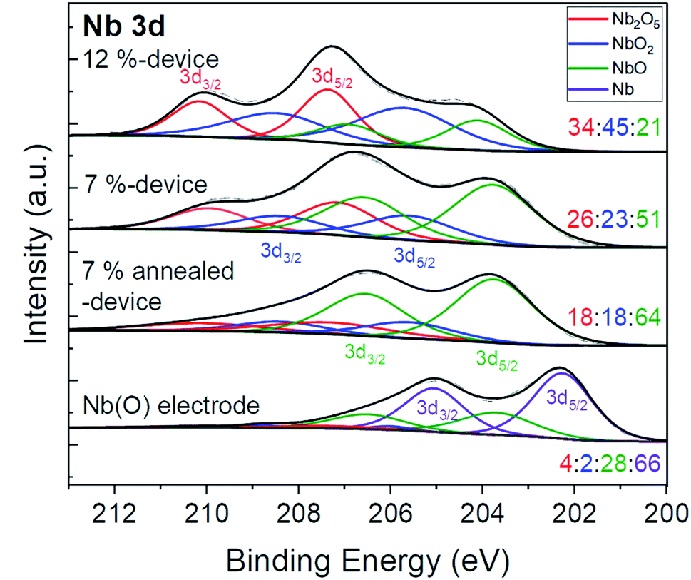 | ||
| Fig. 11 Nb 3d spectra of the Nb(O) electrode and the NbOx layers in the 12%-, 7%-, and 7%-annealed devices. | ||
As illustrated in Fig. 2, the threshold switching mechanism in the Nb(O)/NbOx/Nb(O) devices is associated with the percolation of conducting phases as conducting filament that depends on the oxygen vacancy concentration with respect to the preparation conditions of NbOx layer. From the XPS results of chemical bonding states analyses of the NbOx layers, the NbOx layers consist of the mixture of insulating Nb2O5 and fairly conducting NbO2 and NbO phases.30 The resistivities of Nb2O5, NbO2, NbO, and Nb are known to be around 1011, 101 ∼ 104, 2 × 10⁻⁵, and 1.5 × 10⁻⁵, respectively.38 The 12%- and 7%-devices require the forming operation for the threshold switching. At forming operation, the content of conducting phases such as NbO2 and NbO is increased as Nb(O) electrodes absorb oxygen atoms and further deplete oxygen from NbOx layer by applied electric field.10,39 The conducting phases are percolated to form conducting filament upon applying the voltage higher than Vth, which would be partially dissolved readily as reducing the voltage to be lower than Vhold and the devices return to be HRS. The HRS current after dissolution of filament is determined by the resistivity of NbOx layer. Thus, the 12%-device with higher content of insulating Nb2O5 phase than other devices has the lowest HRS current. On the other hand, because the 7% annealed-device has the increased content of conducting phases settled in the NbOx layer by post-annealing, the forming-free threshold switching could be obtained readily by the alignment of conducting phases upon applying the voltage.
Since the threshold switching is strongly related with the compositions and phases of NbOx layers, the interaction with electrodes plays an important role in threshold switching behaviors.13,40 Because the reaction of Nb + 2Nb2O5 → 5NbO2 is thermodynamically favorable with Gibbs free energy of formation ΔGfo = −164.3 kJ mol−1,41 the reduction of Nb2O5 to enrich oxygen-depleted conducting phases would be facilitated in the device with Nb(O) electrode by the post-annealing or application of electrical bias. Even with the reduction of Nb2O5, because the Nb(O) electrodes have substantial oxygen content of almost 40 at%, it restricts excessive migration of oxygen atoms from NbOx layer. Thus, the overgrowth of conducting filament could be effectively prevented and reliable threshold switching could be obtained. These results indicate that the precise control of oxygen amount in the NbOx switching layer by deposition and annealing processes and the proper interaction with Nb(O) electrodes are crucial for reliable threshold switching characteristics of the Nb(O)/NbOx/Nb(O) devices.
4. Conclusion
The bipolar threshold switching characteristics of the Nb(O)/NbOx/Nb(O) devices with respect to the preparation conditions of the NbOx layers are demonstrated. The 12%-device with NbOx switching layer deposited at 12% of O2 gas mixed in Ar shows threshold switching behavior at Vth < ±2 V after forming operation at Vf of about +4 V. The 7%-device with NbOx layer deposited at 7% of O2 gas is also found to require forming operation but with the lower Vf of around +2 V, and subsequent threshold switching at Vth < ±2 V. Notably, the 7% annealed-device with post-annealing process exhibits the forming-free threshold switching behaviors as a result of increased contents of conducting NbO and NbO2 phases by post-annealing. The LRS/HRS ratios are in the range from 10 to 20 in the 7%-device and from 30 to 100 in the 12%-device, respectively. The cycle–to cycle and cell-to-cell distributions of Vth and Vf values are found to be fairly uniform with maximum deviation < 20% from randomly chosen devices. The voltage pulse measurements disclose the switching time < 100 ns. From the composition and chemical bonding state analyses, the NbOx layers have the approximate ratio of Nb:O = 1:1.9 with the mixture of Nb2O5, NbO2, and NbO phases with different relative fractions. The fraction of insulating Nb2O5 phase is about 34% in the 12%-device, which is the highest among three devices, so the forming operation with the highest Vf is required. On the other hand, the fraction of Nb2O5 is about 18% in the 7% annealed-device, which is the lowest and then renders the forming-free threshold switching operation. The threshold switching mechanism is associated with the percolation of conducting phases, which is determined by the NbOx layer preparation conditions and the interaction with Nb(O) electrodes. The Nb(O) electrodes have substantial oxygen content of almost 40 at%, which prevents excessive redistribution of oxygen atoms, then enables the reliable threshold switching characteristics. The results of threshold switching in these devices demonstrate that the precise control of oxygen amount in the NbOx switching layer by appropriate interaction with the Nb(O) electrodes through post-deposition annealing is an effective route to realize the forming-free threshold switching characteristics for the application to selector devices in high-density crossbar array architectures.
Author contributions
Kitae Park: conceptualization, data curation, formal analysis, investigation, writing – original draft. Jiyeon Ryu: data curation, formal analysis. Dwipak Prasad Sahu: writing – review & editing. Hyun-Mi Kim: data curation, formal analysis. Tae-Sik Yoon: funding acquisition, project administration, supervision, visualization, writing – review & editing.Conflicts of interest
There are no conflicts to declare.Acknowledgements
This research was supported by National R&D Program through the National Research Foundation of Korea(NRF) funded by Ministry of Science and ICT(NRF-2021M3F3A2A01037844). This work was supported by the National Research Foundation of Korea(NRF) funded by Korea Government (MSIT) (NRF-2020R1F1A1049160). This research was supported by Material Innovation Leading Project through the National Research Foundation of Korea (NRF) funded by the Ministry of Science and ICT (2020M3H4A3081879).References
- R. Waser and M. Aono, Nanoionics-based resistive switching memories, Nat. Mater., 2007, 6, 833–840 CrossRef CAS PubMed.
- J. J. S. Yang, D. B. Strukov and D. R. Stewart, Memristive devices for computing, Nat. Nanotechnol., 2013, 8, 13–24 CrossRef CAS PubMed.
- R. Waser, R. Dittmann, G. Staikov and K. Szot, Redox-based resistive switching memories - nanoionic mechanisms, prospects, and challenges, Adv. Mater., 2009, 21, 2632–2663 CrossRef CAS.
- E. Linn, R. Rosezin, C. Kugeler and R. Waser, Complementary resistive switches for passive nanocrossbar memories, Nat. Mater., 2010, 9, 403–406 CrossRef CAS PubMed.
- C. Yakopcic, T. M. Taha and R. Hasan, Hybrid crossbar architecture for a memristor based memory, Proc. IEEE Natl. Aerosp. Electron. Conf., 2014, 237–242 Search PubMed.
- B. S. Kang, S. E. Ahn, M. J. Lee, G. Steftinovich, K. H. Kim, W. X. Xianyu, C. B. Lee, Y. Park, I. G. Baek and B. H. Park, High-current-density CuOx/ZnOx thin-film diodes for cross-point memory applications, Adv. Mater., 2008, 20, 3066–3069 CrossRef CAS.
- B. J. Choi, J. M. Zhang, K. Norris, G. Gibson, K. M. Kim, W. Jackson, M. X. M. Zhang, Z. Y. Li, J. J. Yang and R. S. Williams, Trilayer tunnel selectors for memristor memory cells, Adv. Mater., 2016, 28, 356–362 CrossRef CAS PubMed.
- P. Narayanan, G. W. Burr, R. S. Shenoy, S. Stephens, K. Virwani, A. Padilla, B. N. Kurdi and K. Gopalakrishnan, Exploring the design space for crossbar arrays built with mixed-ionic-electronic-conduction (MIEC) access devices, IEEE J. Electron Devices Soc., 2015, 3, 423–434 CAS.
- R. S. Shenoy, G. W. Burr, K. Virwani, B. Jackson, A. Padilla, P. Narayanan, C. T. Rettner, R. M. Shelby, D. S. Bethune, K. V. Raman, M. BrightSky, E. Joseph, P. M. Rice, T. Topuria, A. J. Kellock, B. Kurdi and K. Gopalakrishnan, MIEC (mixed-ionic-electronic-conduction)-based access devices for non-volatile crossbar memory arrays, Semicond. Sci. Technol., 2014, 29, 104005 CrossRef.
- J. Park, E. Cha, I. Karpov and H. Hwang, Dynamics of electroforming and electrically driven insulator-metal transition in NbOx selector, Appl. Phys. Lett., 2016, 108, 232101 CrossRef.
- Y. H. Wang, R. B. Comes, S. A. Wolf and J. W. Lu, Threshold switching characteristics of Nb/NbO2/TiN vertical devices, IEEE J. Electron Devices Soc., 2016, 4, 11–14 Search PubMed.
- H. Maehne, H. Wylezich, S. Slesazeck, T. Mikolajick, J. Vesely, V. Klemm and D. Rafaja, Room temperature fabricated NbOx/Nb2O5 memory switching device with threshold switching effect, 5th IEEE International Memory Workshop, 2013, pp. 174–177 Search PubMed.
- J. Aziz, H. Kim, S. Rehman, M. F. Khan and D. K. Kim, Chemical nature of electrode and the switching response of RF-sputtered NbOx Films, Nanomaterials, 2020, 10, 2164 CrossRef CAS PubMed.
- E. Cha, J. Park, J. Woo, D. Lee, A. Prakash and H. Hwang, Comprehensive scaling study of NbO2 insulator-metal-transition selector for cross point array application, Appl. Phys. Lett., 2016, 108, 153502 CrossRef.
- S. Slesazeck, H. Mahne, H. Wylezich, A. Wachowiak, J. Radhakrishnan, A. Ascoli, R. Tetzlaff and T. Mikolajick, Physical model of threshold switching in NbO2 based memristors, RSC Adv., 2015, 5, 102318–102322 RSC.
- Y. M. Sun, C. Song, S. Q. Yin, L. L. Qiao, Q. Wan, R. Wang, F. Zeng and F. Pan, Design of a controllable redox-Diffusive threshold switching memristor, Adv. Electron. Mater., 2020, 6, 2000695 CrossRef CAS.
- Z. R. Wang, M. Y. Rao, R. Midya, S. Joshi, H. Jiang, P. Lin, W. H. Song, S. Asapu, Y. Zhuo, C. Li, H. Q. Wu, Q. F. Xia and J. J. Yang, Threshold switching of Ag or Cu in dielectrics: materials, mechanism, and applications, Adv. Funct. Mater., 2018, 28, 1704862 CrossRef.
- Q. L. Hua, H. Q. Wu, B. Gao, M. R. Zhao, Y. J. Li, X. Y. Li, X. Hou, M. F. Chang, P. Zhou and H. Qian, A threshold switching selector based on highly ordered Ag nanodots for x-point memory applications, Adv. Sci., 2019, 6, 1900024 CrossRef PubMed.
- H. Zheng, H. J. Kim, P. Yang, J. S. Park, D. W. Kim, H. H. Lee, C. J. Kang and T. S. Yoon, Forming-free resistive switching characteristics of Ag/CeO2/Pt devices with a large memory window, Semicond. Sci. Technol., 2017, 32, 055006 CrossRef.
- M. Ismail, C. Y. Huang, D. Panda, C. J. Hung, T. L. Tsai, J. H. Jieng, C. A. Lin, U. Chand, A. Rana, E. Ahmed, I. Talib, M. Nadeem and T. Y. Tseng, Forming-free bipolar resistive switching in nonstoichiometric ceria films, Nanoscale Res. Lett., 2014, 9, 1–8 CrossRef PubMed.
- Y. C. Yang, P. Gao, S. Gaba, T. Chang, X. Q. Pan and W. Lu, Observation of conducting filament growth in nanoscale resistive memories, Nat. Commun., 2012, 3, 1–8 Search PubMed.
- W. Wang, M. Wang, E. Ambrosi, A. Bricalli, M. Laudato, Z. Sun, X. D. Chen and D. Ielmini, Surface diffusion-limited lifetime of silver and copper nanofilaments in resistive switching devices, Nat. Commun., 2019, 10, 1–9 CrossRef PubMed.
- C. H. Huang, T. S. Chou, J. S. Huang, S. M. Lin and Y. L. Chueh, Self-selecting resistive switching scheme using TiO2 nanorod arrays, Sci. Rep., 2017, 7, 1–9 CrossRef PubMed.
- H. J. Kim, H. Zheng, J. S. Park, D. H. Kim, C. J. Kang, J. T. Jang, D. H. Kim and T. S. Yoon, artificial synaptic characteristics with strong analog memristive switching in a Pt/CeO2/Pt structure, Nanotechnology, 2017, 28, 285203 CrossRef PubMed.
- T. S. Lee, N. J. Lee, H. Abbas, H. H. Lee, T. S. Yoon and C. J. Kang, Compliance current-controlled conducting filament formation in tantalum oxide-based RRAM devices with different top electrodes, ACS Appl. Electron. Mater., 2020, 2, 1154–1161 CrossRef CAS.
- C. L. Liu, G. K. Ma, J. P. Zeng, Q. Y. Tan, Z. Q. Zhang, A. Chen, N. F. Liu, H. Z. Wan, B. Y. Wang, L. Tao, Y. H. Rao, L. P. Shen, H. B. Wang, J. Zhang and H. Wang, Research on improving the working current of NbOx-based selector by inserting a Ti layer, Frontiers in Materials, 2021, 8, 301 Search PubMed.
- J. Liang and H. S. P. Wong, Cross-point memory array without cell selectors-device characteristics and data storage pattern dependencies, IEEE Trans. Electron Devices, 2010, 57, 2531–2538 Search PubMed.
- C. T. Wu, Intrinsic stress of magnetron-sputtered niobium films, Thin Solid Films, 1979, 64, 103–110 CrossRef CAS.
- G. Brauer, Die oxyde des niobs, Z. Anorg. Allg. Chem., 1941, 248, 1–31 CrossRef CAS.
- V. V. Atuchin, I. E. Kalabin, V. G. Kesler and N. V. Pervukhina, Nb 3d and O 1s core levels and chemical bonding in niobates, J. Electron Spectrosc. Relat. Phenom., 2005, 142, 129–134 CrossRef CAS.
- J. C. Schwanebeck, R. H. Buitrago, L. E. Toth, A. M. Goldman and R. Cantor, Auger-electron analysis of oxygen contamination in sputter-deposited Nb films, J. Appl. Phys., 1978, 49, 848–851 CrossRef CAS.
- M. Fenn, A. K. Petford-Long and P. E. Donovan, Electrical resistivity of Cu and Nb thin films and multilayers, J. Magn. Magn. Mater., 1999, 198–99, 231–232 CrossRef.
- F. J. Wong, N. N. Hong and S. Ramanathan, Orbital splitting and optical conductivity of the insulating state of NbO2, Phys. Rev. B, 2014, 90, 115135 CrossRef.
- L. S. Huang, J. W. Wu, P. Han, A. M. Al-Eniz, T. M. Almutairi, L. J. Zhang and G. F. Zheng, NbO2 electrocatalyst toward 32% faradaic efficiency for N-2 fixation, Small Methods, 2019, 3, 1800386 CrossRef.
- K. Islam, R. Sultana, B. Satpati and S. Chakraborty, Studies on structural and dielectric properties of NbO2-Nb2O5 thin-film-based devices, Vacuum, 2022, 195, 110675 CrossRef CAS.
- N. B. S. Pakpoom Buabthong, S. Mitrovic and N. S. Lewis, Vanadium, niobium and tantalum by XPS, Surf. Sci. Spectra, 2017, 24, 024001 CrossRef.
- H. Tian, C. E. Reece, M. J. Kelley, S. C. Wang, L. Plucinski, K. E. Smith and M. M. Nowelle, Surface studies of niobium chemically polished under conditions for superconducting radio frequency (SRF) cavity production, Appl. Surf. Sci., 2006, 253, 1236–1242 CrossRef CAS.
- C. Nico, T. Monteiro and M. P. F. Graca, Niobium oxides and niobates physical properties: Review and prospects, Prog. Mater. Sci., 2016, 80, 1–37 CrossRef CAS.
- S. K. Nandi, X. J. Liu, D. K. Venkatachalam and R. G. Elliman, Threshold current reduction for the metal-insulator transition in NbO2-x-selector devices: the effect of ReRAM integration, J. Phys. D: Appl. Phys., 2015, 48, 195105 CrossRef.
- K. L. Lin, T. H. Hou, J. Shieh, J. H. Lin, C. T. Chou and Y. J. Lee, Electrode dependence of filament formation in HfO2 resistive-switching memory, J. Appl. Phys., 2011, 109, 084104 CrossRef.
- I. Barin, Thermochemical data of pure substances, VCH Publishers, New York, 3rd edn, 1995 Search PubMed.
| This journal is © The Royal Society of Chemistry 2022 |