
 Open Access Article
 This Open Access Article is licensed under a Creative Commons Attribution-Non Commercial 3.0 Unported Licence
Growth of turbostratic stacked graphene using waste ferric chloride solution as a feedstock†
Piyaporn Surinlertac,
Phurida Kokmatb and
Akkawat Ruammaitree *bc
*bc
aChulabhorn International College of Medicine, Thammasat University, Pathum Thani 12120, Thailand
bDepartment of Physics, Faculty of Science and Technology, Thammasat University, Pathum Thani 12120, Thailand. E-mail: u4605070@hotmail.com
cThammasat University Research Unit in Synthesis and Applications of Graphene, Thammasat University, Pathum Thani 12120, Thailand
First published on 2nd September 2022
Abstract
Monolayer graphene has excellent electrical properties especially a linear dispersion in the band structure at the K-point in the Brillouin zone. However, its electronic transport properties can be degraded by surface roughness and attachment of charge impurities. Although multilayer graphene can reduce the surface roughness and attachment of charge impurities, the increase in the number of graphene layers can degrade the electronic transport properties due to interlayer interactions. Turbostratic graphene can significantly reduce the effect of interlayer interaction of multilayer graphene resulting in electrical properties similar to those of monolayer graphene. In this report, we have demonstrated the growth of turbostratic stacked graphene using waste ferric chloride solution as a feedstock by vaporization and calcination at 700 °C for 6 hours under an argon atmosphere. SEM images and EDX elemental distribution maps showed graphene can be grown on iron and nickel catalysts. XRD results and Raman spectra confirmed the presence of turbostratic stacked graphene with the interlayer spacing in the range of 3.41 Å to 3.44 Å. The Raman spectra in all samples also displayed a weak intensity peak of iTALO− and a well-fitted 2D band by a single Lorentzian peak indicating the presence of turbostratic stacked graphene. In addition, XPS spectra reveal the growth mechanism of the turbostratic stacked graphene. This synthesis process of turbostratic stacked graphene is not only simple, low-cost, and suitable for large-scale production but also decreases the environmental issues from releasing waste ferric chloride solution with improper disposal.
Introduction
Graphene is a monolayer of carbon atoms arranged in a honeycomb crystal lattice. Graphene has attracted attention from many researchers due to its exotic properties such as high electron mobility,1 linear dispersion (Dirac cone) at the K-point in the Brillouin zone,2 high intrinsic strength3 and superior thermal conductivity.4 However, these desirable properties, especially electrical properties, can be degraded with an increase in the number of graphene layers due to the interlayer interactions between adjacent graphene layers. In theory, monolayer graphene should have the best electronic transport properties because of no interlayer interaction, but realistically its electronic transport properties can be degraded by surface roughness5 and attachment of charge impurities.6 High levels of the surface roughness and charge impurities can often appear on the monolayer graphene because it has only single carbon atom thick.Turbostratic stacked graphene is multilayer graphene which contains the relative rotations between adjacent graphene layers. The interlayer rotations of turbostratic graphene can reduce the effect of interlayer interaction leading to the linear dispersion and carrier mobilities similar to those of monolayer graphene.7 In addition, the turbostratic stacked multilayer graphene has lower level of surface roughness and charge impurities than monolayer graphene resulting in its conductivity and carrier mobility are higher than those of the monolayer graphene.8 Therefore, the turbostratic multilayer graphene is a promising candidate material for the application of high-performance electronic devices.
Chemical vapor deposition (CVD)9 is generally utilized for the growth of graphene sheet because it can provide large-area graphene at low cost.10 Nickel is commonly utilized as metal catalyst for the growth of multilayer graphene by CVD.11 After the CVD growth procedure, the nickel catalyst must be etched by immersion in the ferric chloride solution.12 The waste ferric chloride solution can cause water pollution and harmful chronic effects on the aquatic biota if it is thrown overboard without proper disposal.13
Various methods for synthesis of graphene powder have been developed to generate high-quality graphene powder with low cost and large-scale production. Micromechanical exfoliation of graphite can produce high-quality graphene monolayer, but the scale production is small.14 The oxidation–reduction method is commonly used to fabricate graphene powder because it can achieve the large-scale production of reduced graphene oxide at low cost. However, the quality of the resultant graphene powder is low due to the presence of high level of deflects and oxygen content on the graphene surface.15 In 2014, Binbin Zhang et al. propose the different method which can achieve mass production of high-quality graphene with low cost by calcinating glucose and ferric chloride solution under argon atmosphere at 700 °C for 6 hours.16 For this method, the iron is utilized as metal catalyst for synthesis of graphene. Nevertheless, nickel is also the metal catalyst which is commonly utilized to synthesis graphene. Therefore, the mixture of iron and nickel can also be utilized as metal catalyst for graphene growth.
In this study, we demonstrated the growth of turbostratic stacked graphene using waste ferric chloride solution as a feedstock. The utilization of the waste ferric chloride solution as a raw material for the synthesis process of turbostratic stacked graphene can not only reduce the cost production of turbostratic stacked graphene but also decrease the environmental issues.
Experimental
Preparation of waste ferric chloride solution
The ferric chloride solution was prepared by dissolving 80 g ferric chloride in 100 ml deionized water. A graphene on nickel foam sample (ESI†) was immersed in the ferric chloride solution for 24 hours to etch nickel. The mass of nickel in the waste solution was calculated by the mass difference of the sample before and after immersion in the ferric chloride solution. In this study, the nickel masses of 0 g, 0.6719 g, 1.6407 g and 2.5981 g was dissolved in the waste solution for studying the growth of turbostratic stacked graphene. The sample names were designated by the mass of nickel dissolved in the waste solution i.e., the GFeNi0, GFeNi0.6719, GFeNi1.6407 and GFeNi2.5981 were prepared by the mixture of 80 g ferric chloride, 100 ml deionized water and the dissolved nickel of 0 g, 0.6719 g, 1.6407 g and 2.5981 g, respectively.Preparation of turbostratic stacked graphene
The 5 ml waste ferric chloride solution and 2 g sucrose were mixed and poured into an alumina crucible boat. Subsequently, the sample was vaporized at 90 °C for 24 hours. After that, the sample was transferred into the quart tube furnace. Before annealing the sample, the argon gas was introduced for 30 minutes to evacuate air in the quartz tube. Thereafter, the sample was calcined in the quartz tube under argon atmosphere at 700 °C for 6 hours. Then the sample was fast cooled down to room temperature under argon atmosphere. The graphene-wrapped metal (iron and nickel) was obtained. The metal in the sample can be eliminated by immersing the sample in 6 M HCl for 6 hours to obtain turbostratic stacked graphene powder.Characterization
Field emission scanning electron microscope (Fe-SEM) and energy-dispersive X-ray spectroscope (EDX) were carried out by Hitachi UHR Fe-SEM SU8010 with incident beam of 20 kV. X-ray diffraction (XRD) measurement was performed using benchtop X-ray powder diffractometer (Bruker) with Cu-Kα radiation (λ = 0.154184 nm). Micro-Raman measurement was conducted at room temperature using a 532 nm laser. The laser beam size is about 1 μm in diameter. X-ray photoelectron spectroscopy (XPS) was measured by Axis Supra, Kratos using 225 W Al-Kα monochromator. The base pressure was about 2.7 × 10⁻⁹ torr.Results and discussion
Fig. 1 shows SEM images and EDX maps of the GFeNi0, GFeNi0.6719, GFeNi1.6407 and GFeNi2.5981. EDX maps display carbon element distributes on all sample surfaces meanwhile nickel element distributes on the sample surfaces of GFeNi0.6719, GFeNi1.6407 and GFeNi2.5981 revealing that graphene can be grown on nickel and iron. In addition, the non-uniform carbon signal implies the non-uniform thickness of graphene. | ||
| Fig. 1 Comparison of SEM images (left column) and EDX elemental distribution maps for carbon (C, orange), chlorine (Cl, white), iron (Fe, green), oxygen (O, blue) and nickel (Ni, red) of GFeNi0, GFeNi0.6719, GFeNi1.6407 and GFeNi2.5981. | ||
XRD results of the GFeNi0, GFeNi0.6719, GFeNi1.6407 and GFeNi2.5981 are displayed in Fig. 2(a). The XRD patterns of all samples show the characteristic of graphene oxide and graphene peak at 2θ of ∼10° and ∼26°, respectively, indicating the presence of graphene oxide and graphene on all samples. The interlayer spacing of graphene oxide is much larger than that of graphene due to the presence of oxygen-containing groups on the edge of each layer.17 In addition, the XRD pattern of GFeNi2.5981 displays the XRD peaks at 2θ of 35.39°, 42.84°, 43.81°, 44.59°, 51.05° and 74.92° which correspond to NiCl2,18 FeCl3,19 Fe2O3 (ref. 20) and NiO,21 Ni21 and Fe,20 Ni,21 NiO,21 respectively, implying that graphene can be grown on the surfaces of nickel and iron. It is in good agreement with EDX results which show Cl, Fe, O and Ni elements distribute on whole sample surface. Fig. 2(b) shows XRD experimental pattern and fitting curve around the graphene peak of GFeNi2.5981. The curve fitting is calculated using the following equation:22
![[thin space (1/6-em)]](https://www.rsc.org/images/entities/char_2009.gif) sinθ)/λ where dj is a graphene layer spacing. θ is an angle between the incident beam and the scatting planes. λ is wavelength of incident X-ray beam. For the graphene peak of GFeNi2.5981, the fitting curve is calculated using the parameters in Table S1.† The calculation curve reveals that the graphene layer spacing is 3.42 Å and the thickness of graphene is non-uniform. The information about the graphene thickness and layer spacing of GFeNi2.5981 is shown in Fig. 2(c) and Table S2.† In addition, the XRD patterns reveal the graphene layer spacings of GFeNi0, GFeNi0.6719, GFeNi1.6407 and GFeNi2.5981 are 3.43 Å, 3.44 Å, 3.44 Å and 3.42 Å, respectively. These graphene layer spacings are much larger than the interlayer spacing of AB-stacked graphene (3.35 Å) implying all samples contain turbostratic stacked graphene.24
sinθ)/λ where dj is a graphene layer spacing. θ is an angle between the incident beam and the scatting planes. λ is wavelength of incident X-ray beam. For the graphene peak of GFeNi2.5981, the fitting curve is calculated using the parameters in Table S1.† The calculation curve reveals that the graphene layer spacing is 3.42 Å and the thickness of graphene is non-uniform. The information about the graphene thickness and layer spacing of GFeNi2.5981 is shown in Fig. 2(c) and Table S2.† In addition, the XRD patterns reveal the graphene layer spacings of GFeNi0, GFeNi0.6719, GFeNi1.6407 and GFeNi2.5981 are 3.43 Å, 3.44 Å, 3.44 Å and 3.42 Å, respectively. These graphene layer spacings are much larger than the interlayer spacing of AB-stacked graphene (3.35 Å) implying all samples contain turbostratic stacked graphene.24
 | ||
| Fig. 2 (a) XRD patterns of GFeNi0, GFeNi0.6719, GFeNi1.6407 and GFeNi2.5981 before etching the metal. (b) XRD experimental results (blue curve) and XRD calculation curve (red curve) of GFeNi2.5981 at graphene peak. (c) Proportion of graphene thickness in the GFeNi2.5981. | ||
Fig. 3(a) presents Raman spectra of GFeNi0, GFeNi0.6719, GFeNi1.6407 and GFeNi2.5981. The results show the characteristic graphene peaks at ∼1570 cm−1 (G band) and ∼2680 cm−1 (2D band) indicating the presence of graphene in all samples. The intensity of G peak is higher than that of 2D peak. It is corresponding to the turbostratic stacked graphene prepared by laser-assisted process25 and direct carbon ions implantation.26 Whereas it is different from the turbostratic stacked graphene prepared by physical vapor deposition (PVD)7 which shows the Raman intensity of 2D peak is significantly greater than that of G peak. In 2009, Casiraghi proved that the intensity of 2D peak drastically decreases when doping increases while the intensity of G peak is independent on the doping.27 Therefore, the synthesis of graphene by different methods may produce turbostratic stacked graphene with different doping. The Raman spectra also show graphene D-band (∼1340 cm−1) which originates from the sp2-hybridized disordered carbon materials.28 Fig. 3(b) displays the intensity ratio of D peak to G peak (D/G) and the graphene grain size of all samples. The graphene grain size is calculated by the following equation:29
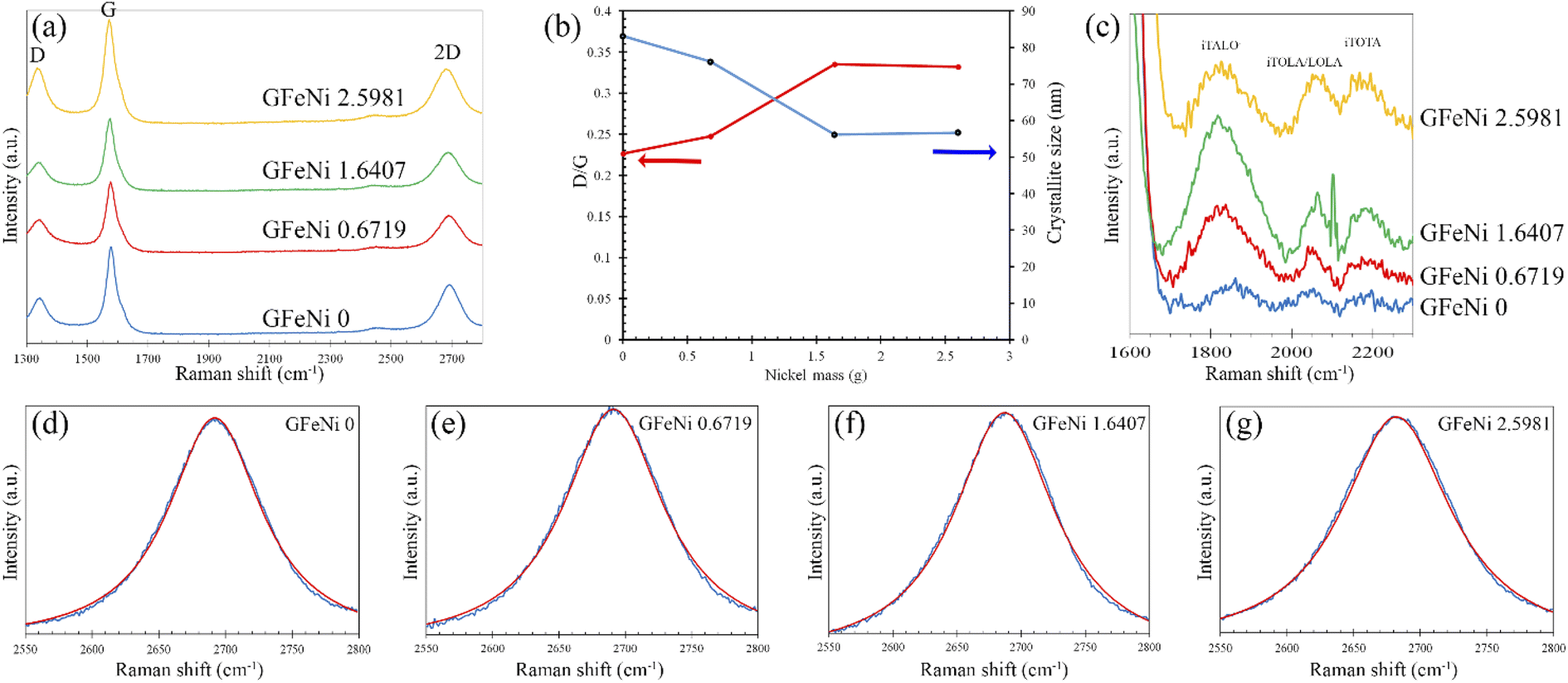 | ||
| Fig. 3 (a) Raman spectra of GFeNi0, GFeNi0.6719, GFeNi1.6407 and GFeNi2.5981. (b) D/G (left axis) and graphene grain size (right axis) of GFeNi0, GFeNi0.6719, GFeNi1.6407 and GFeNi2.5981. (c) Magnified Raman spectra (after baseline subtraction) between 1600 cm−1 and 2300 cm−1 of GFeNi0, GFeNi0.6719, GFeNi1.6407 and GFeNi2.5981. (d)–(g) Experimental Raman spectra (blue) and single Lorentzian fit (red) of the 2D band of GFeNi0, GFeNi0.6719, GFeNi1.6407 and GFeNi2.5981, respectively. | ||
M band (∼1750 cm−1) is an overtone of the oTO phonon. M band has been observed in bilayer and few-layer AB stacked graphene and highly ordered pyrolytic graphite (HOPG) because the M band is activated by strong interlayer interactions between adjacent graphene layers.30 The M band is absent for single layer graphene and turbostratic stacked graphene. Therefore the absence of M band from the samples implies that the stacking pattern of graphene on all samples is turbostratic. It is in good agreement with the XRD results. Fig. 3(d)–(g) display the curve fitting on Raman spectra of 2D band of GFeNi0, GFeNi0.6719, GFeNi1.6407 and GFeNi2.5981 that can well fit using a single Lorentzian peak (red) with the full width at half maximum (FWHM) of 85 cm−1, 92 cm−1, 96 cm−1 and 100, respectively. These FWHM values are corresponding to the turbostratic stacked graphene prepared by laser-assisted process25 and direct carbon ions implantation.26 Whereas, these FWHM values are much higher than that of monolayer graphene (∼24 cm−1)24 and the turbostratic stacked graphene prepared by PVD (27–65 cm−1). Although the FWHM of these samples is wide and similar to AB stacked multilayer graphene (∼100 cm−1),7 the well-fitted 2D band by a single Lorentzian peak in all samples can confirm the structure of graphene is turbostratic stacking. In addition, the single Lorentzian fit can reveal the value of the c-axis lattice constant using the following empirical formula31
 and
and  are the intensities of the single Lorentzian peak and its coexisting Lorentzian, respectively, at 2D band. Since all samples can be well fit by a single Lorentzian peak, the
  vanishes resulting in the c-axis lattice constant and interlayer spacing of graphene is 0.682 nm and 0.341 nm, respectively (the interlayer spacing of graphene is half of the value of c-axis lattice constant32). The interlayer spacing of 3.41 Å is near the XRD results that reveal the graphene layer spacings of GFeNi0, GFeNi0.6719, GFeNi1.6407 and GFeNi2.5981 are 3.43 Å, 3.44 Å, 3.44 Å and 3.42 Å, respective.
The vaporization is an important process to arrange carbon atoms around the metal before the growth of graphene by calcination at 700 °C. Fig. 4 shows XPS spectra of the C 1s of the GFeNi0 before and after calcination at 700 °C for 6 hours. The XPS spectrum of GFeNi0 before calcination process is deconvoluted into 5 peaks at 283.0 eV, 284.6 eV, 286.3 eV, 287.5 eV and 289.1 eV, which correspond to the bonds of C–Fe, C–C (sp3), C–O, C![[double bond, length as m-dash]](https://www.rsc.org/images/entities/char_e001.gif) O and O–CO, respectively. The high intensity peak of C–Fe implies that after the sample underwent the vaporization process, the metal catalyst is surrounded by amorphous carbon and the C–Fe bonds occur between the metal catalyst and its nearest carbon atoms. After calcination at 700 °C for 6 hours, the XPS spectrum of the GFeNi0 is deconvoluted into 5 peaks at 284.1 eV, 285.2 eV, 286.2 eV, 288.3 eV and 290.5 eV, which correspond to the bonds of CC (sp2), C–C (sp3), C–O, CO and O–CO, respectively. The peak areas of C–O bond, CO bond and O–CO bond decrease significantly due to the carbon oxidation.33 The dominant CC (sp2) corresponds to the π-bonded carbon atoms of the graphene network.34 However, the C–Fe peak is absent from the XPS spectrum indicating there is not C–Fe bonding between iron and the first carbon layer (innermost carbon layer). Therefore, the first carbon layer is graphene layer. Fig. 4 also displays the XPS spectra of the C 1s of GFeNi0.6719, GFeNi1.6407 and GFeNi2.5981. A peak at ∼281.7 eV corresponds to C–Ni bonds. The peak area of C–Ni bond increases when nickel content increases. The binding energy of this C–Ni peak is lower than that of nickel carbide thin film (283.3 eV).35 The presence of C–Ni bonds implies that there are C–Ni bonds between nickel and the first carbon layer (innermost carbon layer). Therefore, the first carbon layer is buffer layer while the second carbon layer is graphene layer. It is similar to the growth of epitaxial graphene on Si-terminated SiC that the first carbon layer is buffer layer which contains Si–C bonds between the first carbon layer and the silicon layer underneath.36,37
O and O–CO, respectively. The high intensity peak of C–Fe implies that after the sample underwent the vaporization process, the metal catalyst is surrounded by amorphous carbon and the C–Fe bonds occur between the metal catalyst and its nearest carbon atoms. After calcination at 700 °C for 6 hours, the XPS spectrum of the GFeNi0 is deconvoluted into 5 peaks at 284.1 eV, 285.2 eV, 286.2 eV, 288.3 eV and 290.5 eV, which correspond to the bonds of CC (sp2), C–C (sp3), C–O, CO and O–CO, respectively. The peak areas of C–O bond, CO bond and O–CO bond decrease significantly due to the carbon oxidation.33 The dominant CC (sp2) corresponds to the π-bonded carbon atoms of the graphene network.34 However, the C–Fe peak is absent from the XPS spectrum indicating there is not C–Fe bonding between iron and the first carbon layer (innermost carbon layer). Therefore, the first carbon layer is graphene layer. Fig. 4 also displays the XPS spectra of the C 1s of GFeNi0.6719, GFeNi1.6407 and GFeNi2.5981. A peak at ∼281.7 eV corresponds to C–Ni bonds. The peak area of C–Ni bond increases when nickel content increases. The binding energy of this C–Ni peak is lower than that of nickel carbide thin film (283.3 eV).35 The presence of C–Ni bonds implies that there are C–Ni bonds between nickel and the first carbon layer (innermost carbon layer). Therefore, the first carbon layer is buffer layer while the second carbon layer is graphene layer. It is similar to the growth of epitaxial graphene on Si-terminated SiC that the first carbon layer is buffer layer which contains Si–C bonds between the first carbon layer and the silicon layer underneath.36,37
 | ||
| Fig. 4 XPS spectra of C 1s of the GFeNi0 before and after calcination process, GFeNi0.6719, GFeNi1.6407, GFeNi2.5981. | ||
Fig. S3(a)† shows XRD patterns of the GFeNi0 prepared with and without vaporization process. The intensity ratio of graphene peak (∼26°) to Fe peak (∼44°) (Igraphene/IFe) for the GFeNi0 prepared with and without vaporization process are 0.72 and 0.33, respectively, revealing that the GFeNi0 prepared with vaporization process contains a higher quantity of graphene since only the carbon atoms near the metal catalyst can be dissolved and formed graphene after the calcination at 700 °C for 6 hours. After the graphene growth process, all samples can be attracted by a magnet (Fig. S3(b)†) due to the presence of metal inside. However, the magnetic property can be removed (Fig. S3(c)†) after etching the metal catalyst inside by immersion in HCl.
The growth mechanism of turbostratic stacked graphene using waste ferric chloride solution as a feedstock is illustrated schematically in Fig. 5. First, the sucrose is dissolved in waste ferric chloride solution. Subsequently, the solution was vaporization at 90 °C for 24 hours resulting in the amorphous carbon surrounds the nickel and iron. The C-metal bonds occur between the metal and the nearest carbon atoms. After that the sample is calcined in the quartz tube under argon atmosphere at 700 °C for 6 hours. At this annealing temperature, the surrounding carbon atoms are dissolved into the nickel and iron. Thereafter the sample is fast cooled down to room temperature, the carbon atoms in the nickel and iron precipitate and form turbostratic stacked graphene encloses the nickel and iron. The formation of turbostratic stacked graphene may arises from the fast heating and cooling rate.25,38,39 However, in the case of nickel metal catalyst, the first carbon layer is buffer layer while the second carbon layer is the first layer of graphene. The layer spacing of the turbostratic stacked graphene is ∼3.42 Å.
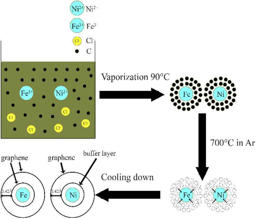 | ||
| Fig. 5 Schematic diagram of growth mechanism of turbostratic graphene using waste ferric chloride solution as a feedstock. | ||
Conclusion
We have demonstrated the growth of turbostratic stacked graphene using waste ferric chloride solution as a feedstock by vaporization at 90 °C for 24 hours and calcination at 700 °C for 6 hours. SEM images and EDX elemental distribution maps showed graphene can be grown on iron and nickel catalysts meanwhile XRD patterns confirm the presence of turbostratic stacked graphene with the interlayer spacing in the range of 3.42 Å to 3.44 Å. Moreover, the Raman spectra display the weak intensity peak of iTALO− and the well-fitted 2D band by a single Lorentzian peak indicating the presence of turbostratic stacked graphene. In addition, XPS spectra reveal the growth mechanism of the turbostratic stacked graphene. The first carbon layer (innermost carbon layer) which surrounds iron is graphene layer meanwhile the first carbon layer which surrounds nickel is buffer layer. This synthesis process of turbostratic stacked graphene is not only simple, low-cost, and large-scale production but also decreases the environmental issues from releasing the waste ferric chloride solution with improper disposal.Conflicts of interest
There are no conflicts to declare.Acknowledgements
This work was supported by the Thailand Science Research and Innovation Fundamental Fund, and Thammasat Univeristy Research Fund, Contract No. TUFT-FF 8/2565, and Thammasat University Research Unit in Synthesis and Applications of Graphene.Notes and references
- A. K. Geim and K. S. Novoselov, Nat. Mater., 2007, 6, 183 CrossRef CAS PubMed.
- T. Ohta, A. Bostwick, J. L. McChesney, T. Seyller, K. Horn and E. Rotenberg, Phys. Rev. Lett., 2007, 98, 206802 CrossRef PubMed; K. V. Emtsev, F. Speck, Th. Seyller and L. Ley, Phys. Rev. B: Condens. Matter Mater. Phys., 2008, 77, 155303 CrossRef.
- I. A. Ovid'ko, Rev. Adv. Mater. Sci., 2013, 34, 1 Search PubMed.
- A. A. Balandin, S. Ghosh, W. Bao, I. Calizo, D. Teweldebrhan, F. Miao and C. N. Lau, Nano Lett., 2008, 8, 902 CrossRef CAS PubMed.
- S. B. Touski and M. Hosseini, Phys. E, 2020, 116, 113763 CrossRef CAS.
- J. Yang, Y. He, X. Zhang, W. Yang, Y. Li, X. Li, Q. Chen, X. Chen, K. Du and Y. Yan, J. Mater. Res. Technol., 2021, 15, 3005 CrossRef CAS.
- J. A. Garlow, L. K. Barrett, L. Wu, K. Kisslinger, Y. Zhu and J. F. Pulecio, Sci. Rep., 2016, 6, 19804 CrossRef CAS PubMed.
- C. Wei, R. Negishi, Y. Ogawa, M. Akabori, Y. Taniyasu and Y. Kobayashi, Jpn. J. Appl. Phys., 2019, 58, SIIB04 CrossRef CAS.
- A. Ruammaitree, Surf. Rev. Lett., 2018, 1840003 CrossRef CAS.
- S. Bae, H. Kim, Y. Lee, X. Xu, J. S. Park, Y. Zheng, J. Balakrishnan, T. Lei, H. R. Kim, Y. Song, Y. J. Kim, K. S. Kim, B. Özyilmaz, J. H. Ahn, B. H. Hong and S. Iijima, Nat. Nanotechnol., 2010, 5, 574 CrossRef CAS PubMed.
- A. Reina, X. Jia, J. Ho, D. Nezich, H. Son, V. Bulovic, M. S. Dresselhaus and J. Kong, Nano Lett., 2009, 9, 30 CrossRef CAS PubMed.
- L. Huang, Q. H. Chang, G. L. Guo, Y. Liu, Y. Q. Xie, T. Wang, B. Ling and H. F. Yang, Carbon, 2012, 50, 551 CrossRef CAS.
- R. B. S. Santos, O. Rocha and J. Povinelli, Chemosphere, 2007, 68, 628 CrossRef PubMed.
- K. S. Novoselov, A. K. Geim, S. V. Morozov, D. Jiang, Y. Zhang, S. V. Dubonos, I. V. Grigorieva and A. A. Firsov, Science, 2004, 306, 666 CrossRef CAS PubMed.
- R. Mangaiyarkarasi, N. Santhiya and S. Umadevi, Colloids Surf., A, 2022, 642, 128673 CrossRef CAS.
- B. Zhang, J. Song, G. Yang and B. Han, Chem. Sci., 2014, 5, 4656 RSC.
- F. T. Johra, J. Lee and W. Jung, J. Ind. Eng. Chem., 2014, 20, 2883 CrossRef CAS.
- Y. Chen, S. Shen, J. Gu, Z. Zhang and N. Li, ACS Omega, 2020, 5, 27278 CrossRef CAS PubMed.
- Sh. M. Nasef, N. A. Badawy, F. H. Kamal, S. F. Sherbiny and E. M. El-Nesr, Arab J. Nucl. Sci. Appl., 2019, 52, 209 Search PubMed.
- S. H. Khezri, A. Yazdani and R. Khordad, Eur. Phys. J.: Appl. Phys., 2012, 59, 30401 CrossRef.
- J. T. Richardson, R. Scates and M. V. Twigg, Appl. Catal., A, 2003, 246, 137 CrossRef CAS.
- A. Ruammaitree, H. Nakahara, K. Akimoto, K. Soda and Y. Saito, Appl. Surf. Sci., 2013, 282, 297 CrossRef CAS.
- P. Brown, A. Fox, E. Maslen, M. O'Keefe and B. Willis, International Tables for Crystallography C, 2004, vol. 6, p. 554 Search PubMed.
- L. M. Malard, M. A. Pimenta, G. Dresselhaus and M. S. Dresselhaus, Phys. Rep., 2009, 473, 51 CrossRef CAS.
- M. Athanasiou, N. Samartzis, L. Sygellou, V. Dracopoulos, T. Loannides and S. N. Yannopoulos, Carbon, 2021, 172, 750 CrossRef CAS.
- K. Liu, F. Lu, K. Li, Y. Xu and C. Ma, Appl. Surf. Sci., 2019, 493, 1255 CrossRef CAS.
- C. Casiraghi, Phys. Rev. B: Condens. Matter Mater. Phys., 2009, 80, 233407 CrossRef.
- M. J. Matthews, M. A. Pimenta, G. Dresselhaus, M. S. Dresselhaus and M. Endo, Phys. Rev. B: Condens. Matter Mater. Phys., 1999, 59, R6585 CrossRef CAS.
- P. Machac and T. Hrebicek, J. Mater. Sci.: Mater. Electron., 2017, 28, 12425 CrossRef CAS.
- R. Rao, R. Podila, R. Tsuchikawa, J. Katoch, D. Tishler, A. M. Rao and M. Ishigami, ACS Nano, 2011, 5, 1594 CrossRef CAS PubMed.
- L. G. Cancado, K. Takai, T. Enoki, M. Endo, Y. A. Kim, H. Mizusaki, N. L. Speziali, A. Jorio and M. A. Pimenta, Carbon, 2008, 46, 272 CrossRef CAS.
- J. Hass, W. A. Heer and E. H. Conrad, J. Phys.: Condens. Matter, 2008, 20, 323202 CrossRef.
- L. Zhou, Chapter 3 – Fundamentals of Combustion Theory, in Theory and Modeling of Dispersed Multiphase Turbulent Reacting Flows, 2018, vol. 15 Search PubMed.
- M. K. Rabchinskii, S. D. Saveliev, D. Y. Stolyarova, M. Brzhezinskaya, D. A. Kirilenko, M. V. Baidakova, S. A. Ryzhkov, V. V. Shnitov, V. V. Sysoev and P. N. Brunkov, Carbon, 2021, 182, 593 CrossRef CAS.
- A. Furlan, J. Lu, L. Hultman, U. Jansson and M. Magnuson, J. Phys.: Condens. Matter, 2014, 26, 415501 CrossRef PubMed.
- A. Ruammaitree, H. Nakahara and Y. Saito, Appl. Surf. Sci., 2014, 307, 136 CrossRef CAS.
- W. Strupinski, K. Grodecki, P. Caban, P. Ciepielewski, I. Jozwik-Biala and J. M. Baranowski, Carbon, 2015, 81, 63 CrossRef CAS.
- S. N. Yannopoulos, A. Siokou, N. K. Nasikas, V. Dracopoulos, F. Ravani and G. N. Papatheodorou, Adv. Funct. Mater., 2012, 22, 113 CrossRef CAS.
- D. X. Luong, K. V. Bets, W. A. Algozeeb, M. G. Stanford, C. Kittrell, W. Chen, R. V. Salvatierra, M. Ren, E. A. McHugh, P. A. Advincula, Z. Wang, M. Bhatt, H. Guo, V. Mancevski, R. Shahsavari, B. I. Yakobson and J. M. Tour, Nature, 2020, 577, 647 CrossRef CAS PubMed.
Footnote |
| † Electronic supplementary information (ESI) available. See https://doi.org/10.1039/d2ra02686d |
| This journal is © The Royal Society of Chemistry 2022 |