
 Open Access Article
 This Open Access Article is licensed under a
 Creative Commons Attribution 3.0 Unported Licence
Fullerene C70/porphyrin hybrid nanoarchitectures: single-cocrystal nanoribbons with ambipolar charge transport properties†
Takatsugu Wakahara *a,
Kahori Nagaokaa,
Chika Hirataa,
Kun'ichi Miyazawab,
Kazuko Fujiia,
Yoshitaka Matsushitac,
Osamu Itoa,
Makito Takagid,
Tomomi Shimazakid,
Masanori Tachikawa*d,
Yoshiki Wadaa,
Shinjiro Yagyua,
Yubin Liue,
Yoshiyuki Nakajimae and
Kazuhito Tsukagoshi*f
*a,
Kahori Nagaokaa,
Chika Hirataa,
Kun'ichi Miyazawab,
Kazuko Fujiia,
Yoshitaka Matsushitac,
Osamu Itoa,
Makito Takagid,
Tomomi Shimazakid,
Masanori Tachikawa*d,
Yoshiki Wadaa,
Shinjiro Yagyua,
Yubin Liue,
Yoshiyuki Nakajimae and
Kazuhito Tsukagoshi*f
aResearch Center for Functional Materials, National Institute for Materials Science, 1-1 Namiki, Tsukuba, Ibaraki 305-0044, Japan. E-mail: Wakahara.Takatsugu@nims.go.jp
bDepartment of Chemical Sciences and Technology, Graduate School of Chemical Sciences and Technology, Tokyo University of Science, 6-3-1 Niijuku, Katsushika-ku, Tokyo 125-8585, Japan
cResearch Network and Facility Services Division, National Institute for Materials Science, 1-2-1 Sengen, Tsukuba, Ibaraki 305-0047, Japan
dQuantum Chemistry Division, Graduate School of NanoBioScience, Yokohama City University, 22-2 Seto, Kanazawa-ku, Yokohama, Kanagawa 236-0027, Japan. E-mail: tachi@yokohama-cu.ac.jp
eRIKEN KEIKI Co., Ltd, 2-7-6, Azusawa, Itabashi-ku, Tokyo 174-8744, Japan
fInternational Center for Materials Nanoarchitectonics (WPI-MANA), National Institute for Materials Science, 1-1 Namiki, Tsukuba, Ibaraki 305-0044, Japan. E-mail: Tsukagoshi.Kazuhito@nims.go.jp
First published on 6th July 2022
Abstract
In recent years, supramolecular cocrystals containing organic donors and acceptors have been explored as active components in organic field-effect transistors (FETs). Herein, we report the synthesis of novel single-cocrystal nanoribbons with ambipolar charge transport characteristics from C70 and 5,10,15,20-tetrakis(3,5-dimethoxyphenyl)porphyrin (3,5-TPP) in a 3![[thin space (1/6-em)]](https://www.rsc.org/images/entities/char_2009.gif) :2 ratio. The C70/3,5-TPP nanoribbons exhibited a new strong absorption band in the near-infrared region, indicating the presence of charge-transfer interactions between C70 and 3,5-TPP in the cocrystals. We elucidated the mechanism of the charge-transport properties of the nanoribbons using photoemission yield spectroscopy in air and theoretical calculations. A strong interaction between porphyrins in the one-dimensional porphyrin chains formed in C70/3,5-TPP nanoribbons, which was confirmed by single-crystal X-ray diffraction, plays a crucial role in their hole transport properties.
:2 ratio. The C70/3,5-TPP nanoribbons exhibited a new strong absorption band in the near-infrared region, indicating the presence of charge-transfer interactions between C70 and 3,5-TPP in the cocrystals. We elucidated the mechanism of the charge-transport properties of the nanoribbons using photoemission yield spectroscopy in air and theoretical calculations. A strong interaction between porphyrins in the one-dimensional porphyrin chains formed in C70/3,5-TPP nanoribbons, which was confirmed by single-crystal X-ray diffraction, plays a crucial role in their hole transport properties.
Introduction
Functional supramolecular nanoarchitectures have tremendous potential as building blocks for bottom-up organic nanoscale electronic devices1–3 such as transistors.4 Recently, several studies have been reported on transistors employing supramolecular nanoarchitectures, such as nanowhiskers, nanotubes, nanorods, nanowires, and nanosheets.1,5,6 A distinct characteristic of almost all these reported transistors is that they transport only a single carrier type, i.e., either holes (p-type) or electrons (n-type). Therefore, simultaneous or selectable transport of electrons and/or holes (ambipolar charge transport) remains a highly desirable device characteristic to be achieved, because this characteristic will be able to facilitate the design of better-performing electronic circuits7 as well as the demonstration of bifunctional organic devices, such as light-emitting8 and light-sensing transistors.9 In 2012, we reported novel ambipolar FETs based on C60/5,10,15,20-tetrakis(4-methoxyphenyl)porphyrinato cobalt(II) (C60/CoTMPP) cocrystals.10 Zhu et al. also reported ambipolar FETs using sulfur-bridged annulene-TCNQ cocrystals.11 Following these earlier studies, various FETs based on donor–acceptor (D–A) cocrystals have been reported.12–14 There are several reports on ambipolar FETs based on novel organic semiconductors in the literature;15,16 however, the preparation of these semiconductors requires complex organic syntheses. In contrast, the co-crystallization process can be conducted by simple mixing of two (or more) molecules and does not involve any complex synthesis protocols. Notably, not all D–A cocrystal-based FETs exhibit ambipolar transport properties, some exhibit the unipolar ones, such as n-type17–20 or p-type.21 Therefore, further research is necessary to understand these characteristics in detail.Herein, we report the preparation of cocrystal nanoribbons from C70 and 5,10,15,20-tetrakis(3,5-dimethoxyphenyl)porphyrin (3,5-TPP) as a pair of electron-acceptor and electron-donor molecules by a simple solution mixing method. These C70/3,5-TPP nanoribbons were used to fabricate bottom-gate/bottom-contact FETs. Despite using a non-optimized device architecture, these FETs exhibited ambipolar transport characteristics. This result is in sharp contrast with our earlier report on C60 analogue (C60/3,5-TPP cocrystals) that showed only n-type behavior.17 We found that the one-dimensional porphyrin chains formed by the strong interaction of porphyrins inside the nanoribbons play a very important role in the hole transport properties of the C70/3,5-TPP nanoribbons.
Experimental section
Preparation and characterization of C70/3,5-TPP nanoribbons
C70/3,5-TPP nanoribbons were prepared by mixing two solutions containing C70 and 3,5-TPP. Specifically, 3 ml of C70-saturated toluene solution was placed in a 9 ml glass bottle and 1 mg of 3,5-TPP in 1 ml of toluene was added to this solution. The mixed solution was then vigorously shaken and stored at 10 °C for 24 h to grow the C70/3,5-TPP nanoribbons. C70/3,5-TPP nanoribbons were collected by filtering the solution and washing with iso-propyl alcohol (IPA). These nanoribbons were stable in dark conditions at room temperature for long periods.The structure and morphology of the obtained nanoribbons were analyzed by scanning electron microscopy (SEM; JEOL JSM-6700F, 5 kV), atomic force microscopy (AFM, JEOL, JSPM-5200), a micro-Raman system (Photon Design) equipped with a semiconductor laser with a wavelength of 532 nm, and a single crystal diffractometer (Rigaku Saturn CCD) using Mo Kα X-ray radiation at 113 K. The diffuse reflectance spectra of the nanoribbons were recorded using a UV-Vis-NIR spectroscope (JASCO V-570) equipped with an integrating sphere. Photoemission yield spectroscopy in air (PYSA) was performed using a RIKEN KEIKI AC-3 photoelectron spectrometer equipped with a monochromatic D2 lamp.
The time-resolved luminescence (TRPL) spectra of materials were measured by excitation with a pulsed laser (100 fs pulse width, 1 kHz repetition frequency) generated by an optical parametric amplifier (Spectra Physics TOPAS Prime). The excitation wavelength for TRPL spectroscopy analysis was 520 nm.
Transistors were fabricated using a previously reported method.17 The electrical transport properties were measured inside a glove box using an Agilent B2902A and Agilent E5272A.
For the first-principles quantum chemical calculations, the Gaussian16 (Revision A.03) program package22 was employed together with our Python-based quantum chemical tool.23 The electronic structures were obtained by using the density functional theory (DFT) at the B3LYP/6-31G(d) level. The molecular orbitals were depicted by using Chemcraft.24
Results and discussion
The nanoribbons are classified as cocrystals of C70 and 3,5-TPP as they are single-phase crystalline materials, composed of two different molecules. Fig. 1 shows optical microscopy and SEM images of the C70/3,5-TPP nanoribbons. Both the images show parallelogram morphology of the nanoribbons. The length and width of the nanoribbons were found to be 15–20 μm and 0.2–0.5 μm, respectively (Fig. S1†). The thickness of the nanoribbons, as determined by SEM and AFM measurements, was in the range of 20–200 nm (Fig. S2†). Fig. 2 shows the diffuse reflectance spectra of the C70/3,5-TPP nanoribbons, C70 crystals, and 3,5-TPP film. It is observed that the C70 crystals prepared using the liquid–liquid interface precipitation method17 showed a broad absorption in the 700–400 nm region, whereas the 3,5-TPP film exhibited strong and weak absorption at approximately 400 nm and 500–600 nm, respectively. The C70/3,5-TPP cocrystals exhibited a new absorption in the longer wavelength region (up to 900 nm). Subtraction of the normalized absorption spectrum of C70 from that of the C70/3,5-TPP cocrystals clearly showed the extra absorption in the range of 900–700 nm (with an absorption maximum at 760 nm), which was referred to as the charge-transfer (CT) absorption band of the C70/3,5-TPP nanoribbons. | ||
| Fig. 1 (a) Optical microscopy image and (b) SEM image of C70/3,5-TPP nanoribbons. | ||
 | ||
| Fig. 2 Diffuse reflectance spectra in Vis and near-infrared regions (K/M: Kubelka–Munk function, which is proportional to absorbance); (a) C70/3,5-TPP nanoribbons, (b) C70 crystals, (c) 3,5-TPP film, (d) subtraction of normalized absorption spectra at 610 nm as shown in (a) and (b). | ||
To understand the CT characteristics under light illumination, we measured the photoluminescence (PL) spectra of the C70/3,5-TPP cocrystals (Fig. 3). The CT fluorescence band was observed in the range of 750–1000 nm with a peak at 800 nm, as a mirror image of the CT absorption band at 760 nm. These CT emission peaks are apparently in longer wavelength regions than the emission of C70-crystals.25 A similar CT band was reported for C60/3,5-TPPcocrystals.17 Based on the appearance of the CT absorption band, we conclude that C70 molecules interact with the nearest 3,5-TPP molecules. These interactions in the ground state lead to the formation of the C70/3,5-TPP cocrystals with alternative arrangement of C70 and 3,5-TPP.
 | ||
| Fig. 3 Steady-state fluorescence spectra of 3,5-TPP crystals (black) and C70/3,5-TPP nanoribbons (red); λex: 520 nm. Inset: Time profiles of fluorescence intensity [λex: 520 nm, λem: 690–730 nm for 3,5-TPP crystals (black)17 and λem: 780–820 nm for C70/3,5-TPP nanoribbons (red)]. | ||
The fluorescence lifetime of the C70/3,5-TPP cocrystals was evaluated from the decay–time profile measured using time-resolved luminescence (TRPL) spectroscopy (inset of Fig. 3). Based on the luminescence decay at 770–810 nm, the lifetime of the CT luminescence was measured as approximately 0.5 ns, which is shorter than those of the 3,5-TPP crystal (approximately 2.5 ns) and C60/3,5-TPP cocrystals (approximately 1.0 ns), which is calculated using the previously reported data.17 The observed CT luminescence lifetime suggests that the short CT-excited lifetime is due to rapid shift in electron distribution from the donor to the acceptor part in the excited CT state.
To investigate the charge transport properties of the C70/3,5-TPP nanoribbons, we fabricated bottom-gate, bottom-contact FETs by drop-casting an IPA solution containing C70/3,5-TPP nanoribbons onto a substrate. The substrate used was pre-patterned with gold source-drain electrodes with a channel length and width of 2–10 μm and 10000 μm, respectively, and SiO2 (300 nm thick) as the gate dielectric. The Au electrodes were treated with self-assembled monolayers of undecanethiol and the SiO2 dielectric interface was rendered hydrophobic by treatment with hexamethyldisilazane. This fabrication method, as developed by Samori et al.,26 is simple and convenient for the qualitative charge-transport characterization of the micrometer-sized single-crystals. Fig. 4 shows the dependence of the drain current (ID) on the gate voltage (VG) of the C70/3,5-TPP nanoribbon FET. The measurements were performed under N2 atmosphere at room temperature under dark conditions after annealing at 353 K. (By annealing at 353 K, we observed the increase of channel current of the devices. The XRD pattern measured after annealing showed that the crystal structure is unchanged even after annealing (Fig. S3†).) The transfer characteristics of the C70/3,5-TPP nanoribbon-based FETs showed a V-shape in which the two arms indicated electron transport (n-type) and hole transport (p-type), respectively. These results are in sharp contrast with previously reported measurements on C60 nanowhisker5- and C60/3,5-TPP cocrystal17-based FETs that showed only n-type behavior. The electron and hole mobilities calculated from the data in Fig. 4 were relatively low, in the order of 8.2 × 10⁻⁵ cm2 V−1 s−1 and 3.1 × 10⁻⁶ cm2 V−1 s−1, respectively. However, we believe that further device optimization can lead to higher carrier mobilities.
 | ||
| Fig. 4 Transfer (ID–VG) characteristics of C70/3,5-TPP nanoribbons recorded in dark conditions. The solid curve displays drain current (ID) as a function of gate voltage (VG), and the dotted curve shows the square root of ID (right vertical axis). | ||
There are many studies in the literature on D–A cocrystal-based FETs reporting n-type, p-type, or ambipolar characteristics;17–21 however, their characteristics and charge transport mechanisms have not yet been fully understood. In order to understand the mechanism of the ambipolar charge transport properties, a comparison of C70/3,5-TPP cocrystals observed in the present study with our earlier report on C60/3,5-TPP cocrystals17 that showed only n-type behavior may be useful.
At first, to realize their electronic structure, we carried out PYSA measurements of C70/3,5-TPP and C60/3,5-TPP cocrystals, 3,5-TPP, and C70 powder. PYSA is a powerful tool for understanding the electronic and electrical properties of molecular semiconductors.27–29 Recently, we succeeded in evaluating the electronic structure of C60/Fc nanosheets with high sensitivities using PYSA.30
The ionization energy (Is) of the C70/3,5-TPP nanoribbons was determined to be 5.71 eV, which is 0.51 eV smaller than that of the C70 powder, similar to that of 3,5-TPP. Fig. 5b shows the energy level diagrams of the C70/3,5-TPP nanoribbons, C60/3,5-TPP cocrystals, 3,5-TPP, and C70, estimated using the measured values of Is and the energy gap (Eg). The Eg values were obtained from the Vis-NIR absorption spectra measured in the present study for the C70/3,5-TPP nanoribbons and the previous study for C60/3,5-TPP cocrystals.17 The energy level diagrams demonstrate that the cocrystallization of C70 with 3,5-TPP enhanced the p-type FET characteristics because of the decreased hole injection barrier between the gold electrode and the highest occupied molecular orbital (HOMO) of the C70/3,5-TPP nanoribbons. Similarly, the Is of the C60/3,5-TPP cocrystals was determined to be 5.72 eV (Fig. S4†), and the calculated energy level of the lowest unoccupied molecular orbital (LUMO) of the C60/3,5-TPP cocrystals is located close to that of C70/3,5-TPP nanoribbons. This indicates that the decrease in the hole injection barrier also takes place in the C60/3,5-TPP cocrystal-FET. Therefore the difference between the charge transport properties of ambipolar C70/3,5-TPP nanoribbons and unipolar (n-type) C60/3,5-TPP cocrystals cannot be explained only by the decrease in the hole injection barrier. Consequently, some other factors such as structural difference must be considered.
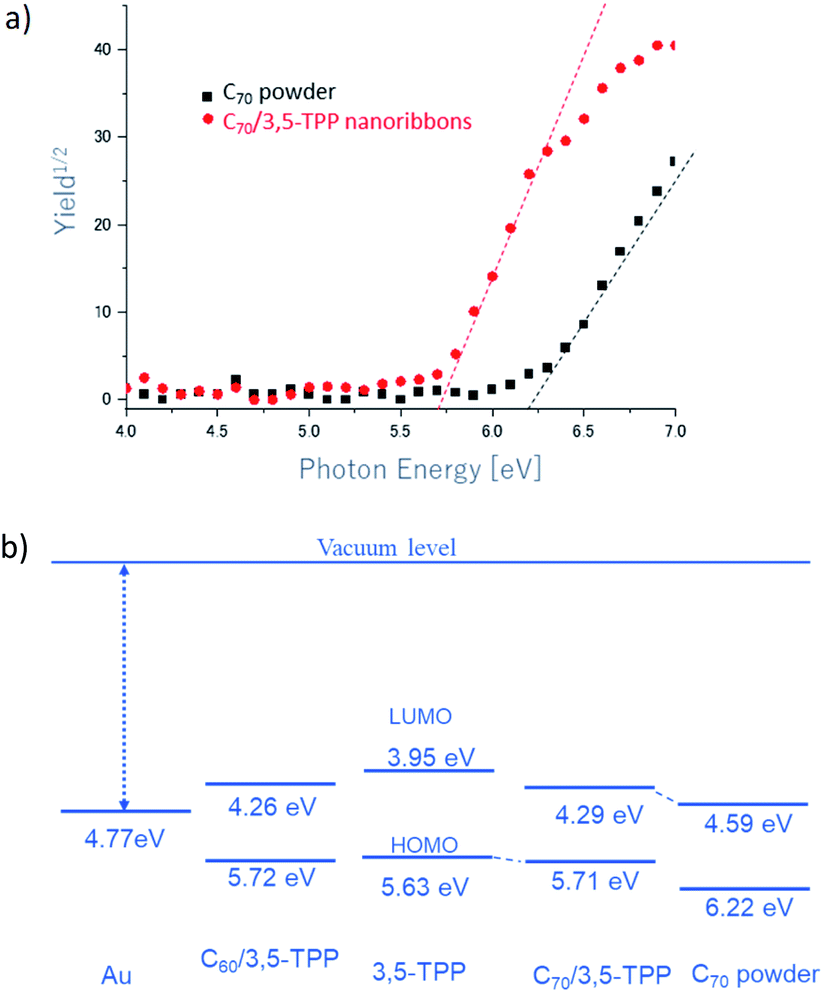 | ||
| Fig. 5 (a) PYSA spectra and (b) energy level diagrams of C60/3,5-TPP cocrystals, 3,5-TPP, C70/3,5-TPP nanoribbons, and C70 powder. For semi-conductor, the HOMO and the LUMO correspond to the top of the valence band and bottom of the conduction band, respectively. | ||
To determine the relationship between the charge transport properties and the molecular arrangement in the C70/3,5-TPP nanoribbon, we determined the crystal structure of the C70/3,5-TPP nanoribbon by single-crystal XRD at 113 K (Fig. 6a). Crystal structure of the C70/3,5-TPP nanoribbon belongs to triclinic ![[P with combining macron]](https://www.rsc.org/images/entities/i_char_0050_0304.gif) 1 space group with the unit cell: a = 13.8828(3) Å, b = 20.9103(5) Å, c = 30.2321(7) Å, α = 84.678(1)°, β = 86.015(1)°, and γ = 84.537(1)° (CCDC-2161616) (Fig. 6). The cocrystal was formulated as [(3,5-TPP)2·(C70)3·(toluene)3] and contained a [C70/(3,5-TPP)/C70]2 unit, in which four C70 molecules assembled above and below the two 3,5-TPP molecular planes (Fig. 6c). The C70 molecules were found to be arranged in zigzag chains that render effective electron transport from one C70 to a nearby C70. This type of [fullerene/(3,5-TPP)/fullerene)] substructure was also observed in the C60/3,5-TPP cocrystal.17 One of the biggest structural differences between the C70/3,5-TPP nanoribbons and C60/3,5-TPP cocrystals is the distance between the nearest 3,5-TPP molecules in the crystal structure. In the C70/3,5-TPP nanoribbons, the 3,5-TPPs were found to be located very close to each other and interacted with the 3,5-dimethoxyphenyl group, resulting in the formation of one-dimensional porphyrin chains (Fig. 6d). The center-to-center distance between the two 3,5-TPP was measured to be approximately 15 Å. Based on the observed results, the most probable mode for electric conduction stems from these porphyrin chains which act as hole-transport pathways in the C70/3,5-TPP nanoribbons by the hopping conduction. One-dimensional porphyrin chains are also formed in C60/3,5-TPP cocrystals. However, the distance between the two 3,5-TPP is approximately 21 Å, because two toluene molecules exist between two 3,5-TPP molecules, which reduces the interaction of the 3,5-TPPs (Fig. S5†). As a result, the C60/3,5-TPP co-crystal exhibited only n-type behavior. Whereas, in the C70/3,5-TPP nanoribbons, toluene molecules are located above the 3,5-TPP molecules (Fig. 6a and b and S6†). These geometrical differences may be related to the fact that ambipolar transport characteristics were observed only for the C70/3,5-TPP nanoribbons, but not for the C60/3,5-TPP cocrystals.
1 space group with the unit cell: a = 13.8828(3) Å, b = 20.9103(5) Å, c = 30.2321(7) Å, α = 84.678(1)°, β = 86.015(1)°, and γ = 84.537(1)° (CCDC-2161616) (Fig. 6). The cocrystal was formulated as [(3,5-TPP)2·(C70)3·(toluene)3] and contained a [C70/(3,5-TPP)/C70]2 unit, in which four C70 molecules assembled above and below the two 3,5-TPP molecular planes (Fig. 6c). The C70 molecules were found to be arranged in zigzag chains that render effective electron transport from one C70 to a nearby C70. This type of [fullerene/(3,5-TPP)/fullerene)] substructure was also observed in the C60/3,5-TPP cocrystal.17 One of the biggest structural differences between the C70/3,5-TPP nanoribbons and C60/3,5-TPP cocrystals is the distance between the nearest 3,5-TPP molecules in the crystal structure. In the C70/3,5-TPP nanoribbons, the 3,5-TPPs were found to be located very close to each other and interacted with the 3,5-dimethoxyphenyl group, resulting in the formation of one-dimensional porphyrin chains (Fig. 6d). The center-to-center distance between the two 3,5-TPP was measured to be approximately 15 Å. Based on the observed results, the most probable mode for electric conduction stems from these porphyrin chains which act as hole-transport pathways in the C70/3,5-TPP nanoribbons by the hopping conduction. One-dimensional porphyrin chains are also formed in C60/3,5-TPP cocrystals. However, the distance between the two 3,5-TPP is approximately 21 Å, because two toluene molecules exist between two 3,5-TPP molecules, which reduces the interaction of the 3,5-TPPs (Fig. S5†). As a result, the C60/3,5-TPP co-crystal exhibited only n-type behavior. Whereas, in the C70/3,5-TPP nanoribbons, toluene molecules are located above the 3,5-TPP molecules (Fig. 6a and b and S6†). These geometrical differences may be related to the fact that ambipolar transport characteristics were observed only for the C70/3,5-TPP nanoribbons, but not for the C60/3,5-TPP cocrystals.
 | ||
| Fig. 6 Crystal structure of a C70/3,5-TPP nanoribbons, (a) [(3,5-TPP)2·(C70)3·(toluene)3] unit structure (b) [(3,5-TPP)2·(C70)3·(toluene)3]2 unit structure (c) the [C70/(3,5-TPP)/C70]2 unit structure, and (d) one-dimensional porphyrin chains unit structure. Red arrows indicate the toluene molecules in the crystals. | ||
For better understanding the hole transport mechanism of cocrystals, we estimated the coupling constant between 3,5-TPPs, based on the DFT method. Fig. 7a and b show inter-molecular structures extracted from C60- and C70-based cocrystals with 3,5-TPP, respectively, where TPPs of the C70-based cocrystal are more densely packed, and the distance between side chains of porphyrin derivatives is shorter, compared with those of C60/3,5-TPP. The coupling constant rapidly decreases with inter-molecular distances, and therefore hole can more easily transport in the C70/3,5-TPP nanoribbons. The first-principles quantum chemical method gives the coupling constant of 4.1 × 10⁻⁴ and 5.3 × 10⁻² eV between TPPs of C60- and C70-based cocrystals, respectively. Here, the coupling constant is estimated from 〈ϕA|HAB|ϕB〉, where ϕA(B) is the molecular orbital of each TPP molecule, and HAB is the Hamiltonian of the whole molecular system. We note that there are several techniques to estimate coupling constants. For example, Krysko et al. employed the multireference quantum chemistry method.31 The generalized Mulliken–Hush method was adopted to calculate electronic couplings for hole transfers in DNA.32 In the coupling constant calculations for the hopping process, the localization of hole may be a key factor. This paper assumes that a hole is localized on each 3,5-TPP site. Fig. 7c and d show that the molecular orbitals of HOMO and HOMO-3 are localized at the center and side-chains of 3,5-TPP, respectively. The coupling constant has a larger value between molecular orbitals localized on side chain, such as seen in Fig. 7d. However, the coupling constant between HOMOs is small (8.8 × 10⁻⁴ eV) even in the C70/3,5-TPP case. We also note that the coupling constant related to HOMO-2 becomes relatively large because of localized orbitals on side chains. The details on molecular orbitals and coupling constants are summarized in the ESI (Fig. S7 and Table S1†). The molecular design on the side chain may be essential to control fast hole transports. Conversely, the large distance between side chains of C60/3,5-TPPs disturbs efficient hole transfers, and results in the n-type behavior of the cocrystal. Thus, the hole conductivity of cocrystal materials is also controlled by higher-order structures such as nanoribbons.
 | ||
| Fig. 7 TPPs structures extracted (a) C60/3,5-TPP and (b) C70/3,5-TPP cocrystals. The distance between porphyrins in C70/3,5-TPP is shorter than that in C60/3,5-TPP. The molecular orbital of (c) HOMO and (d) HOMO-3, which are localized at the center and side chains of TPP, respectively. The interaction between side chains of 3,5-TPPs gives a larger coupling constant. | ||
Conclusions
We successfully constructed supramolecular nanoarchitectures (nanoribbons) comprising C70 and 3,5-TPP in a 3:2 ratio using a simple solution mixing method. The C70/3,5-TPP nanoribbons exhibited ambipolar transport characteristics with nearly balanced hole/electron mobilities. This result is in sharp contrast with our earlier report on C60/3,5-TPP cocrystals, which showed only n-type behavior. Single-crystal X-ray diffraction showed that one-dimensional porphyrin chains with zigzag C70 arrangement are formed in C70/3,5-TPP cocrystals. Our theoretical calculations show the one-dimensional porphyrin chains formed by the strong interactions through the side chains of porphyrins play a very important role in the hole transport properties of C70/3,5-TPP nanoribbons, in addition to the low electron injection barrier. Meanwhile, in the case of C60/3,5-TPP cocrystals, the interaction between porphyrins is reduced owing to the presence of two toluene molecules between porphyrins, which hinder hole transport from one porphyrin to a nearby porphyrin in the C60/3,5-TPP cocrystals. These observations are also supported by the theoretical calculations.
In recent years, numerous organic semiconductors with narrow bandgaps have been synthesized to fabricate ambipolar FETs. In the present study, we developed a distinctive method to prepare ambipolar materials without synthesizing new narrow-bandgap organic semiconductors. The successful preparation of nanoarchitectures with unique electronic characteristics by a simple co-crystallization method can be considered as an important stepping stone toward the fabrication of novel nanoscale devices.
Author contributions
K. N. and C. H. fabricated and characterized the devices. K. i. N., K. F., and O. I. contributed to the interpretation of the experimental results. Y. M. performed single-crystal XRD analysis. Y. W. measured TRPL spectra. M. T. and T. S. performed theoretical calculations. S. Y., Y. L., and Y. N. measured the PYSA. M. T., K. T., and T. W. conducted the experiments and prepared the manuscript. All authors contributed equally to write and approve the final version of the manuscript.Conflicts of interest
There are no conflicts to declare.Acknowledgements
The authors thank the support from Namiki Foundry at the National Institute for Materials Science (NIMS) for the preparation of the pre-patterned substrates. Part of this study was financially supported by a Grant-in-Aid for Scientific Research (No. JP15K05615) from the Ministry of Education, Culture, Sports, Science and Technology, Japan. The computations were partially performed using the ITO computer system at Kyushu University through the HPCI System Research Project (Project ID: hp200075).Notes and references
- F. S. Kim, G. Ren and S. A. Jenekhe, Chem. Mater., 2011, 23, 682–732 CrossRef CAS.
- L. Zang, Y. Che and J. S. Moore, Acc. Chem. Res., 2008, 41, 1596–1608 CrossRef CAS PubMed.
- Y. S. Zhao, H. Fu, A. Peng, Y. Ma, Q. Liao and J. Yao, Acc. Chem. Res., 2010, 43, 409–418 CrossRef CAS PubMed.
- J. Zaumseil and H. Sirringhaus, Chem. Rev., 2007, 107, 1296–1323 CrossRef CAS PubMed.
- H. Li, B. C. K. Tee, J. J. Cha, Y. Cui, J. W. Chung, S. Y. Lee and Z. Bao, J. Am. Chem. Soc., 2012, 134, 2760–2765 CrossRef CAS PubMed.
- S. N. Chen, Z. Li, Y. L. Qiao and Y. L. Song, J. Mater. Chem. C, 2021, 9, 1126–1149 RSC.
- T. D. Anthopoulos, S. Setayesh, E. Smits, M. Colle, E. Cantatore, B. de Boer, P. W. M. Blom and D. M. de Leeuw, Adv. Mater., 2006, 18, 1900–1904 CrossRef CAS.
- J. Zaumseil, R. H. Friend and H. Sirringhaus, Nat. Mater., 2006, 5, 69–74 CrossRef CAS.
- T. D. Anthopoulos, Appl. Phys. Lett., 2007, 91, 113513 CrossRef.
- T. Wakahara, P. D'Angelo, K. i. Miyazawa, Y. Nemoto, O. Ito, N. Tanigaki, D. D. C. Bradley and T. D. Anthopoulos, J. Am. Chem. Soc., 2012, 134, 7204–7206 CrossRef CAS PubMed.
- J. Zhang, H. Geng, T. S. Virk, Y. Zhao, J. Tan, C.-a. Di, W. Xu, K. Singh, W. Hu, Z. Shuai, Y. Liu and D. Zhu, Adv. Mater., 2012, 24, 2603–2607 CrossRef CAS PubMed.
- Y. Wang, W. Zhu, H. Dong, X. Zhang, R. Li and W. Hu, Top. Curr. Chem., 2016, 374, 83 CrossRef PubMed.
- J. Zhang, J. Q. Jin, H. X. Xu, Q. C. Zhang and W. Huang, J. Mater. Chem. C, 2018, 6, 3485–3498 RSC.
- Y. Wang, L. J. Sun, C. Wang, F. X. Yang, X. C. Ren, X. T. Zhang, H. L. Dong and W. P. Hu, Chem. Soc. Rev., 2019, 48, 1492–1530 RSC.
- A. Zampetti, A. Minotto and F. Cacialli, Adv. Funct. Mater., 2019, 29, 1807623 CrossRef.
- L. X. Shi, Y. L. Guo, W. P. Hu and Y. Q. Liu, Mater. Chem. Front., 2017, 1, 2423–2456 RSC.
- T. Wakahara, K. Nagaoka, A. Nakagawa, C. Hirata, Y. Matsushita, K. Miyazawa, O. Ito, Y. Wada, M. Takagi, T. Ishimoto, M. Tachikawa and K. Tsukagoshi, ACS Appl. Mater. Interfaces, 2020, 12, 2878–2883 CrossRef CAS PubMed.
- X. Liu, W. Wang, Z. Fan, W. Huang, L. Luo, C. Yang, J. Zhang, J. Zhao, L. Zhang and W. Huang, Chem.–Eur. J., 2021, 27, 10448–10455 CrossRef CAS PubMed.
- Z. R. Wang, F. Yu, J. Xie, J. F. Zhao, Y. Zou, Z. P. Wang and Q. H. Zhang, Chem.–Eur. J., 2020, 26, 3578–3585 CrossRef CAS PubMed.
- A. Mandal, A. Choudhury, P. K. Iyer and P. Mal, J. Phys. Chem. C, 2019, 123, 18198–18206 CrossRef CAS.
- S. S. Zheng, J. W. Zhong, W. Matsuda, P. Jin, M. Q. Chen, T. Akasaka, K. Tsukagoshi, S. Seki, J. Zhou and X. Lu, Nano Res., 2018, 11, 1917–1927 CrossRef CAS.
- M. J. Frisch, G. W. Trucks, H. B. Schlegel, G. E. Scuseria, M. A. Robb, J. R. Cheeseman, G. Scalmani, V. Barone, G. A. Petersson, H. Nakatsuji, X. Li, M. Caricato, A. V. Marenich, J. Bloino, B. G. Janesko, R. Gomperts, B. Mennucci, H. P. Hratchian, J. V. Ortiz, A. F. Izmaylov, J. L. Sonnenberg, D. Williams-Young, F. Ding, F. Lipparini, F. Egidi, J. Goings, B. Peng, A. Petrone, T. Henderson, D. Ranasinghe, V. G. Zakrzewski, J. Gao, N. Rega, G. Zheng, W. Liang, M. Hada, M. Ehara, K. Toyota, R. Fukuda, J. Hasegawa, M. Ishida, T. Nakajima, Y. Honda, O. Kitao, H. Nakai, T. Vreven, K. Throssell, J. A. Montgomery Jr, J. E. Peralta, F. Ogliaro, M. J. Bearpark, J. J. Heyd, E. N. Brothers, K. N. Kudin, V. N. Staroverov, T. A. Keith, R. Kobayashi, J. Normand, K. Raghavachari, A. P. Rendell, J. C. Burant, S. S. Iyengar, J. Tomasi, M. Cossi, J. M. Millam, M. Klene, C. Adamo, R. Cammi, J. W. Ochterski, R. L. Martin, K. Morokuma, O. Farkas, J. B. Foresman, and D. J. Fox, Gaussian 16, Revision A.03, Gaussian, Inc., Wallingford CT, 2016 Search PubMed.
- T. Shimazaki, M. M. Hashimoto and T. Maeda, Proceedings of the 3rd International Workshop on Software Engineering for High Performance Computing in Computational Science and Engineering, Austin Texas, 2015, vol. 9, DOI:10.1145/2830168.2830170.
- Chemcraft – graphical software for visualization of quantum chemistry computations, https://www.chemcraftprog.com, accessed Mar. 24, 2022 Search PubMed.
- T. Xu, N. Chen, Z. He, P. Yu, W. Shen, T. Akasaka and X. Lu, Chem.–Eur. J., 2021, 27, 10387–10393 CrossRef CAS PubMed.
- M. El Gemayel, M. Treier, C. Musumeci, C. Li, K. Mullen and P. Samori, J. Am. Chem. Soc., 2012, 134, 2429–2433 CrossRef PubMed.
- Y. Nakajima, M. Hoshino, D. Yamashita and M. Uda, Advances in Quantum Chemistry, Academic Press, 2003, vol. 42, pp. 399–405 Search PubMed.
- Y. Nakayama, S. Machida, T. Minari, K. Tsukagishi, Y. Noguchi and H. Ishii, Appl. Phys. Lett., 2008, 93, 269901 CrossRef.
- K. Nakano, Y. Kaji and K. Tajima, ACS Appl. Mater. Interfaces, 2021, 13, 28574–28582 CrossRef CAS PubMed.
- D. Mahdaoui, C. Hirata, K. Nagaoka, K. Miyazawa, K. Fujii, T. Ando, M. Abderrabba, O. Ito, M. Takagi, T. Ishimoto, M. Tachikawa, S. Yagyu, Y. B. Liu, Y. Nakajima, Y. Nemoto, K. Tsukagoshi and T. Wakahara, J. Mater. Chem. C, 2022, 10, 3770–3774 RSC.
- I. D. Krysko, A. Y. Freidzon and A. A. Bagaturyants, Phys. Chem. Chem. Phys., 2020, 22, 3539–3544 RSC.
- T. Shimazaki, Y. Asai and K. Yamashita, J. Phys. Chem. B, 2005, 109, 1295–1303 CrossRef CAS PubMed.
Footnote |
| † Electronic supplementary information (ESI) available: Experimental details. CCDC 2161616. For ESI and crystallographic data in CIF or other electronic format see https://doi.org/10.1039/d2ra02669d |
| This journal is © The Royal Society of Chemistry 2022 |