
 Open Access Article
 This Open Access Article is licensed under a Creative Commons Attribution-Non Commercial 3.0 Unported Licence
The direct growth of planar and vertical graphene on Si(100) via microwave plasma chemical vapor deposition: synthesis conditions effects†
Š. Meškinis *a,
A. Vasiliauskasa,
A. Guobienėa,
M. Talaikisb,
G. Niaurab and
R. Gudaitisa
*a,
A. Vasiliauskasa,
A. Guobienėa,
M. Talaikisb,
G. Niaurab and
R. Gudaitisa
aInstitute of Materials Science, Kaunas University of Technology, K. Baršausko St. 59, LT51423 Kaunas, Lithuania. E-mail: sarunas.meskinis@ktu.lt
bDepartment of Organic Chemistry, Center for Physical Sciences and Technology, Saulėtekio av. 3, LT-10257 Vilnius, Lithuania
First published on 28th June 2022
Abstract
In the present research, graphene was synthesized directly on a Si(100) substrate via combining direct microwave plasma-enhanced chemical vapor deposition and protective enclosure. The graphene flake orientation was controlled using suitable synthesis conditions. We revealed that high processing temperatures and plasma powers promote vertical graphene growth. The main related physical mechanisms were raised temperature gradients, thermal stress, ion bombardment, and elevated electric field effects. Lowering the synthesis temperature and plasma power resulted in planar graphene growth. An elevated synthesis temperature and long deposition time decreased the graphene layer number as the carbon desorption rate increased with temperature. Dominating defect types and their relationships to the graphene growth conditions were revealed. Planar graphene n-type self-doping was found due to substrate-based charge transfer. In the case of vertical graphene, the increased contact area between graphene and air resulted in the adsorption of more molecules, resulting in no doping or p-type doping.
1 Introduction
The 2D nanomaterial graphene is of very significant interest due to its exciting combination of electrical, optical, and mechanical properties. High levels of charge carrier mobility and multiplication, optical transparency, flexibility, very high Young's modulus and failure strength, high ductility, and chemical inertness are all present.1–4 Graphene can be grown as “classic” planar sheets, as vertical graphene flakes and nanowalls, and as a filler in nanocomposite materials. Among the numerous possible graphene applications, it has been considered for use as a new transparent conductor, a monolayer alternative to Schottky contact metals, and even as an active layer in semiconductor devices and different sensors. In particular, vertical graphene nanowalls provide a high surface area that is beneficial for the fabrication of biosensors and energy-storage devices.5 Planar graphene is beneficial for transparent electronics and transparent conductor applications, such as in various photoelectric and microelectronics devices.5Usually, planar graphene is fabricated via graphite exfoliation or chemical vapor deposition (CVD) on catalytic metal (Cu, Ni, Co) foil, with subsequent transfer to the target substrate.6 Graphene transfer onto the target semiconductor or dielectric substrate is a long process. This can result in graphene contamination by different adsorbents7 or the formation of wrinkles or ripples on graphene.8
Graphene can be synthesized directly on semiconducting or dielectric substrates using plasma-enhanced chemical vapor deposition (PECVD). Usually, remote plasma systems are used for direct graphene synthesis to avoid radiation-based defect formation or even the total etching-out of the growing graphene film.9 In such a way, planar graphene layers are grown.9,10 Vertical graphene sheets and nanowalls are synthesized in direct plasma systems.9
Some studies have shown the growth of vertical and planar graphene in the same PECVD system on dielectric or semiconducting substrates.5,11–16
Switching between the growth of planar and vertical graphene on a glass substrate can be achieved using a copper-foam-based Faraday cage with different pore sizes.5 However, this method has some disadvantages. Copper atoms can be deposited on the graphene.17 It was found that the density of graphene nanowalls directly grown on SiO2 and Al2O3 substrates via microwave PECVD can be reduced via combining a protective metallic shield with lowered acetylene/hydrogen gas flow ratios.11 However, planar graphene was grown on the entire substrate surface only when using additional NH3 gas flow.11 Thus, only n-type doped graphene could be achieved. In that study, no details regarding the geometric parameters of the protective shield were provided. Planar and non-planar graphene flakes were synthesized on SiO2 film using a microwave plasma torch.12 The graphene orientation was changed upon choosing an appropriate ethanol gas flow and plasma power in that study. However, the separate planar graphene flakes covered only a tiny part of the substrate.12
In some studies, the graphene flake orientation was changed via controlling the methane and etching gas flow ratios without reporting the use of Faraday-cage-type protective shields. Notably, vertical graphene was grown on silicon via microwave PECVD using CH4/H2 gas flow ratios higher than 5.5, and horizontal graphene was synthesized using lower methane/hydrogen gas flow ratios.13 However, in other studies, vertical graphene was grown using very different CH4/H2 gas flow ratios, and no planar graphene was reported.18–20
The orientation of graphene flakes directly synthesized on SiO2 film was changed from planar to vertical via varying the CH4/Ar gas flow ratio in a CH4![[thin space (1/6-em)]](https://www.rsc.org/images/entities/char_2009.gif) :Ar:H2 gas mixture in an ECR PECVD system.14,15 However, in numerous studies, vertical graphene was grown on SiO2 and other substrates from a CH4:H2 mixture without any argon gas (see reviews18,21–26). On the other hand, planar graphene was synthesized on SiO2 and glass substrates via ECR PECVD using a C2H4:Ar gas mixture.27 The addition of CO2 gas to the methane, hydrogen, and argon gas mixture to grow graphene on glass and quartz substrates using magnetron microwave PECVD resulted in planar graphene rather than vertical graphene.16 However, other authors grew vertical graphene from a CH4/CO2 gas mixture28 or even CO2 gas alone.29 Thus, changing the graphene sheet orientation via adjusting the synthesis gas flow ratio or composition seems to be very system specific.
:Ar:H2 gas mixture in an ECR PECVD system.14,15 However, in numerous studies, vertical graphene was grown on SiO2 and other substrates from a CH4:H2 mixture without any argon gas (see reviews18,21–26). On the other hand, planar graphene was synthesized on SiO2 and glass substrates via ECR PECVD using a C2H4:Ar gas mixture.27 The addition of CO2 gas to the methane, hydrogen, and argon gas mixture to grow graphene on glass and quartz substrates using magnetron microwave PECVD resulted in planar graphene rather than vertical graphene.16 However, other authors grew vertical graphene from a CH4/CO2 gas mixture28 or even CO2 gas alone.29 Thus, changing the graphene sheet orientation via adjusting the synthesis gas flow ratio or composition seems to be very system specific.
In the present research, we achieved control of the orientation of PECVD-synthesized graphene flakes via setting appropriate growth process conditions. The main technological parameters affecting the graphene structure and flake orientation were considered. Those parameters are plasma power, pressure, the gas mixture composition, temperature, and time.18,21,26,30 Technological processing conditions beneficial for the growth of planar graphene and vertical graphene on Si(100) substrates were found. High processing temperatures and plasma powers promoted vertical graphene growth due to increased temperature gradients, thermal stress, ion bombardment, and electric field effects. The suppression of these effects using lower synthesis temperatures and plasma powers promoted planar graphene growth.
2 Experimental
Vertical and planar graphene was synthesized on Si(100) using a Cyrannus microwave-plasma-enhanced chemical vapor deposition (PECVD) system (Innovative Plasma Systems (Iplas) GmbH, Germany). More information on the Cyrannus microwave plasma source can be found elsewhere.31–35 A methane and hydrogen gas mixture was applied. Prime grade n-type double-sided polished monocrystalline Si(100) (Sil'tronix, France) was used. The selected graphene samples were grown on p-Si. According to the manufacturer data, the silicon wafer resistivity was in the range of 1–10 Ω cm. The size of the silicon substrates was 1 × 1 cm.First, the substrate was pretreated with hydrogen plasma without any wet chemical cleaning of the silicon. The plasma power was 1.7 kW, the processing temperature was 900 °C, the hydrogen flow was 200 sccm, the pressure was 22 mBar, and the time was 15 min. After plasma treatment, methane gas was introduced. A special enclosure, consisting of a rectangular non-magnetic steel sheet bent perpendicularly in two places, was used to protect the sample from direct plasma action and prevent excessive etching of the growing graphene. The steel enclosure can withstand much higher processing temperatures and powers without being damaged or without graphene poisoning due to evaporation or sputtering products. We were not able to grow graphene inside the plasma discharge zone when no protective enclosure was used.36 Furthermore, a graphene sample placed inside CH4/H2 plasma without the protective enclosure was fully etched-out.
The graphene synthesis process parameters (plasma power, pressure, methane and hydrogen gas flows, temperature, and time) were varied. The sample direct synthesis conditions are presented in Table 1.
| Sample no. | P, kW | H2, sccm | CH4, sccm | p, mBar | T, °C | t, min |
|---|---|---|---|---|---|---|
| a The graphene was grown on both n-Si and p-Si. | ||||||
| 1 | 1.4 | 150 | 50 | 22 | 900 | 50 |
| 2 | 1.1 | 150 | 50 | 22 | 900 | 50 |
| 3 | 0.9 | 150 | 50 | 22 | 900 | 50 |
| 4 | 0.7 | 150 | 50 | 22 | 900 | 50 |
| 5 | 0.7 | 150 | 50 | 10 | 900 | 50 |
| 6 | 0.7 | 150 | 50 | 10 | 800 | 50 |
| 7 | 0.7 | 150 | 50 | 10 | 700 | 50 |
| 8 | 0.7 | 75 | 25 | 10 | 900 | 50 |
| 9 | 0.7 | 75 | 25 | 10 | 800 | 50 |
| 10 | 0.7 | 75 | 25 | 10 | 700 | 50 |
| 11 | 0.7 | 75 | 35 | 22 | 700 | 50 |
| 12a | 0.7 | 75 | 35 | 10 | 700 | 50 |
| 13 | 1.7 | 150 | 50 | 22 | 800 | 50 |
| 14 | 1.7 | 150 | 50 | 22 | 700 | 50 |
| 15 | 1.7 | 150 | 50 | 22 | 600 | 50 |
| 16 | 1.7 | 150 | 50 | 22 | 900 | 50 |
| 17 | 1.7 | 150 | 50 | 22 | 900 | 30 |
| 18 | 1.7 | 150 | 50 | 22 | 900 | 70 |
| 19 | 1.7 | 150 | 50 | 22 | 900 | 10 |
| 20 | 1.7 | 150 | 50 | 22 | 900 | 90 |
| 21 | 1.7 | 150 | 50 | 10 | 900 | 90 |
| 22 | 0.7 | 150 | 50 | 10 | 900 | 90 |
| 23 | 0.7 | 150 | 50 | 10 | 800 | 90 |
| 24 | 0.7 | 75 | 25 | 10 | 800 | 90 |
| 25 | 0.7 | 75 | 25 | 10 | 700 | 90 |
| 26 | 0.7 | 75 | 25 | 10 | 700 | 150 |
Raman scattering spectra (further Raman spectra) of synthesized samples were acquired using an inVia Raman spectrometer (Renishaw, Wotton-under-Edge, UK). The exciting laser-beam wavelength was 532 nm, and the power was 1.5 mW. The Lorentz function was used to fit the D, G, D′, and 2D peaks. The 2D/G peak intensity ratio (I(2D)/I(G) ratio) was estimated to evaluate the graphene layer number.37 The I(D)/I(G) peak intensity ratio was calculated to estimate the defect density of graphene.38,39 It should be mentioned that the I(2D)/I(G) ratio can decrease depending on the defect density.38 However, a different dependence was found for most samples in our case (Fig. S1†). Thus, we used the I(2D)/I(G) ratio for graphene layer number evaluation, despite the presence of defects. The D/D′ peak intensity ratio revealed the types of dominating defects.43 The full width at half maximum of the G peak (FWHM(G))40–42 and positions of the G and 2D peaks (Pos(G) and Pos(2D))36,41,42,44,45 were also taken into account as parameters sensitive to graphene doping and stress. The spectra were measured in several different places on the sample. Average values and standard deviations of different Raman spectra parameters were calculated for each sample.
Raman mapping was accomplished for selected samples using an inVia Raman microscope (Renishaw, Wotton-under Edge, United Kingdom) equipped with a thermoelectrically cooled (−70 °C) CCD camera. Spectra were excited using 532 nm laser radiation and dispersed using a grating with 1800 lines per mm. The laser power was restricted to 0.45 mW and focused on a spot on the surface with a diameter of approximately 1 μm by using a 50×/0.75 NA objective lens (Leica). The Raman maps were collected from a surface area of 50 × 50 μm2 with a 1.5 μm step size. The acquisition time for each spectrum was set to 4 s. To plot the I(2D)/I(G) maps, experimental spectra were fitted with a single Gaussian–Lorentzian shape component for each of the spectral modes (G and 2D) using software written in our lab based on MATLAB R2013 (The MathWorks Ins.).
Atomic force microscopy (AFM) experiments were carried out at room temperature using a NanoWizardIII atomic force microscope (JPK Instruments, Bruker Nano GmbH, Berlin, Germany). The data were analyzed using JPKSPM data processing software (Version spm-4.3.13, JPK Instruments, Bruker Nano GmbH). The AFM images were collected using an ACTA (Applied NanoStructures, Inc., Mountain View, USA) probe. A pyramidal cantilever was used. The radius of curvature (ROC) was <10.0 nm and the cone angle was 20°. The reflex side coating was Al with a thickness of 50 ± 5 nm. The probe force constant was set at 40 N m−1, and the resonance frequency was in the 300 kHz range. Height, amplitude, and phase diagrams were recorded in steps with a scan size of 2 μm and a scan speed of 1 Hz. The integral gain was set to 2, while the proportional gain was set to 5. Pixels for samples and lines were 516 × 516, operating in tapping mode.
Some samples were additionally investigated using a Helios Nanolab 650 scanning electron microscope (SEM) (FEI, Eindhoven, The Netherlands).
3 Results and discussion
3.1 Synthesis of planar and vertical graphene
The structures of the graphene layers synthesized using different growth process conditions were investigated via Raman spectroscopy. Typical Raman spectra are presented in Fig. 1 and S2.† The G and 2D peaks typical of graphene can be seen at ∼1600 cm−1 and ∼2700 cm−1. Defect-related D (∼1350 cm−1), D + D′′ (∼2500 cm−1), and D + D′ (∼2900 cm−1) peaks39 were observed. The D′ peak at ∼1620 cm−1 is present as a shoulder of the G peak. The presence of defect-related Raman bands is typical for graphene films directly synthesized on silicon and silicon-based dielectrics, such as SiO2 and Si3N4, due to the nanocrystalline nature of these layers.9,10,43 The Si-substrate-related peak at 520 cm−1 (ref. 19 and 46) is visible in the Raman spectra of our samples; the broad feature in the vicinity of 950–1000 cm−1 corresponds to the silicon first overtone mode.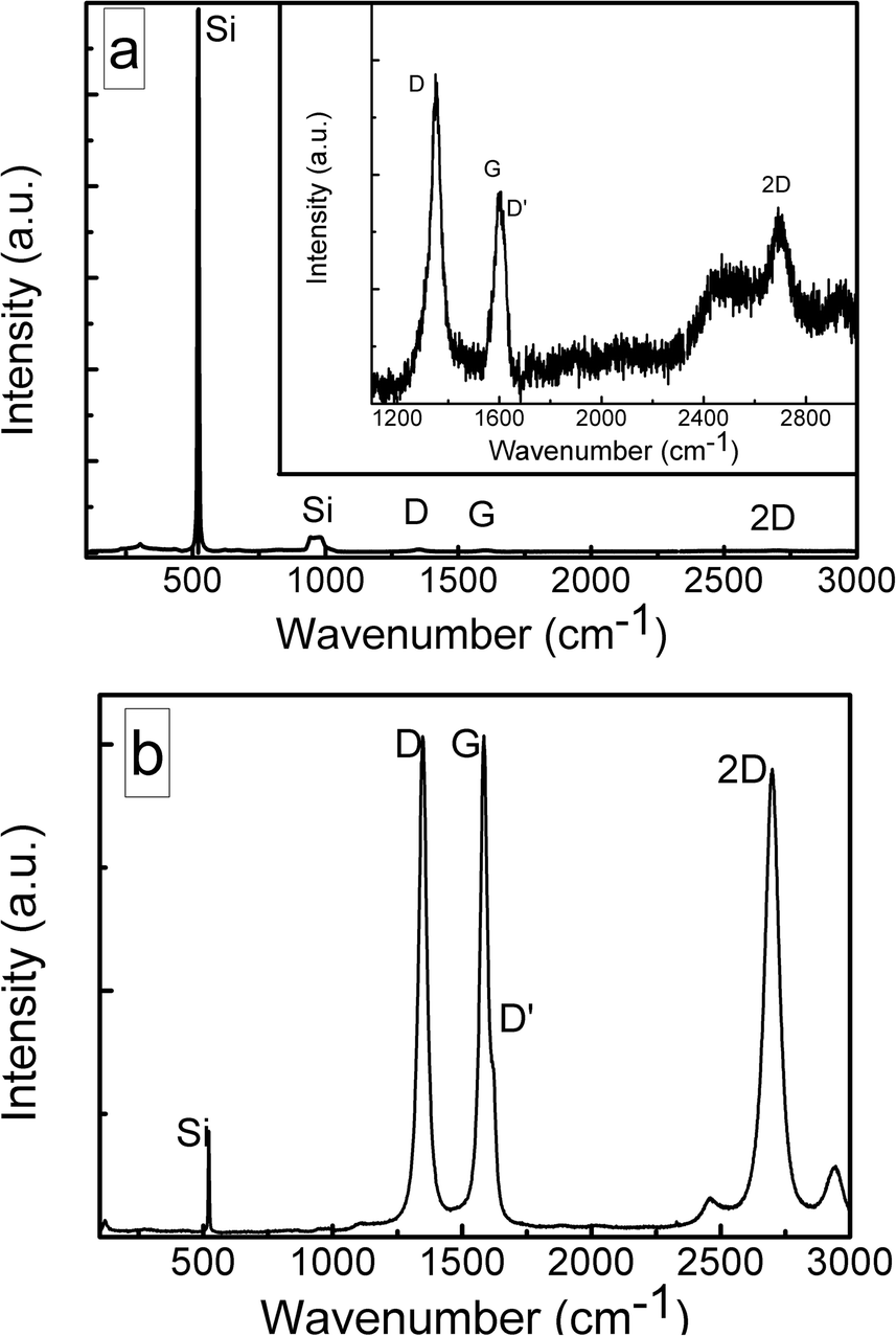 | ||
| Fig. 1 Characteristic Raman spectra of graphene grown on Si(100): (a) the plasma power was 0.7 kW and the synthesis temperature was 700 °C; (b) the plasma power was 1.7 kW and the synthesis temperature was 900 °C. | ||
Significant differences between the synthesized graphene Raman spectra were found. The Si(100) substrate-related peak at 520 cm−1 was much stronger than the graphene-related peaks for some samples. In other cases, the intensity of the G peak was comparable with the intensity of the Si-related peak or it was even higher.
It should be noted that the number of graphene layers can be evaluated based both on the relative intensities of the Si and G bands and the I(2D)/I(G) ratio.46,47 The I(G)/I(Si) ratio should increase and the I(2D)/I(G) ratio should decrease with an increased graphene layer number. It should be mentioned that the I(2D)/I(G) intensity ratio can decrease not only due to an increase in the number of graphene layers but also because of an increase in the disorder/defective nature of a sample.38 However, as discussed above, in our case this ratio can be used to study the graphene layer number changes in different samples (Fig. S1†). The plot of I(2D)/I(G) vs. I(G)/I(Si) revealed contradictory results (Fig. 2a). Three groups of samples were found. For the first group, the I(2D)/I(G) ratio decreased with an increase in the I(G)/I(Si) ratio. In numerous studies, the presence of this behavior for Raman spectra of planar graphene samples indicates a rising graphene layer number.46,47 For the second group, the tendency of the I(2D)/I(G) ratio to rise with the I(G)/I(Si) ratio is seen. In the case of samples with the highest I(G)/I(Si) ratios, no clear relationship is found between the I(2D)/I(G) ratio and I(G)/I(Si) ratio. These contradictory results can be explained via considering different mechanisms affecting the dependence of the I(2D)/I(G) and I(G)/I(Si) ratios on the graphene layer number.46,47 The I(2D)/I(G) ratio is related to changes inside graphene.46,47 At the same time, the I(G)/I(Si) ratio depends on silicon substrate signal attenuation.46 In such a case, the orientation of the graphene flakes can be crucial because vertical graphene nanowalls can absorb several tens of times more light than planar graphene with the same layer number.48 Thus, one can suppose that for vertical graphene nanowalls the I(G)/I(Si) ratio does not depend on the graphene layer number. The selected samples were studied via atomic force microscopy (AFM) and scanning electron microscopy (SEM) to test this assumption (Fig. 2b, 3, and 4, and S4–S21†).
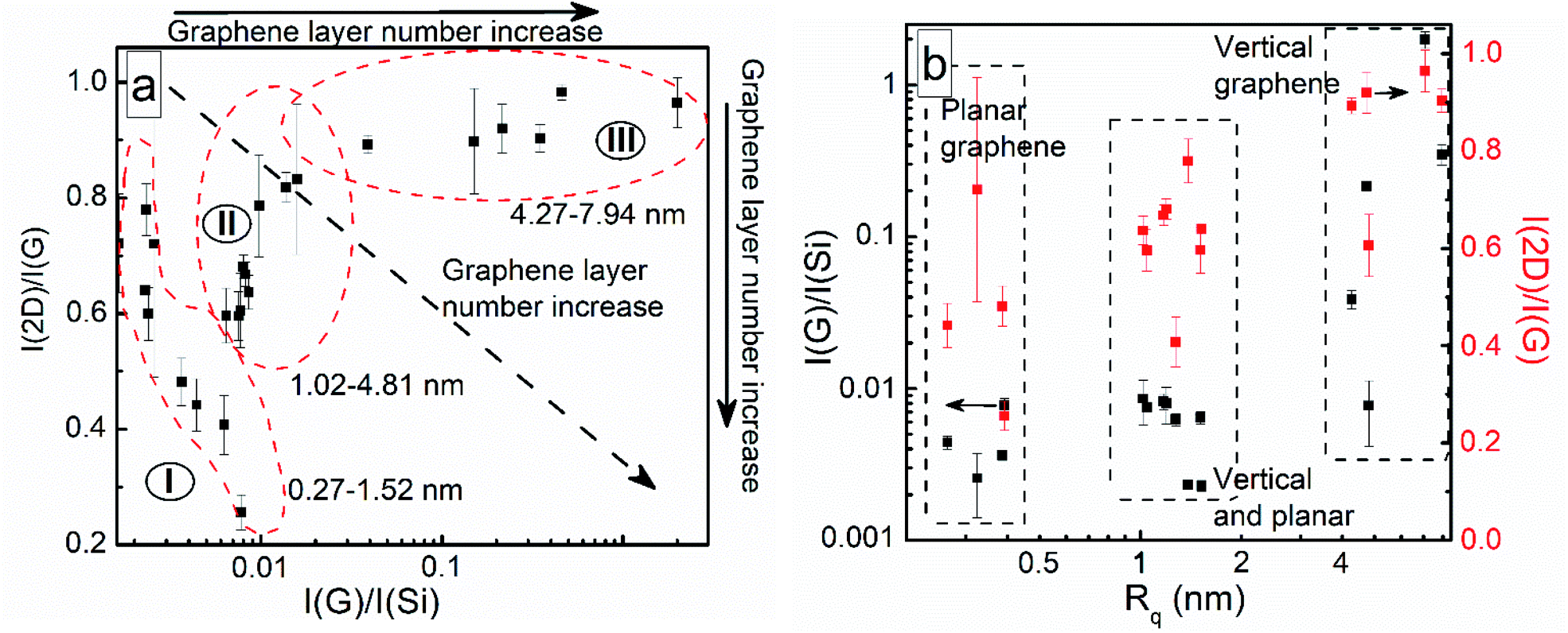 | ||
| Fig. 2 (a) A plot of I(2D)/I(G) vs. I(G)/I(Si); and (b) plots of I(G)/I(Si) vs. Rq and I(2D)/I(G) vs. Rq. | ||
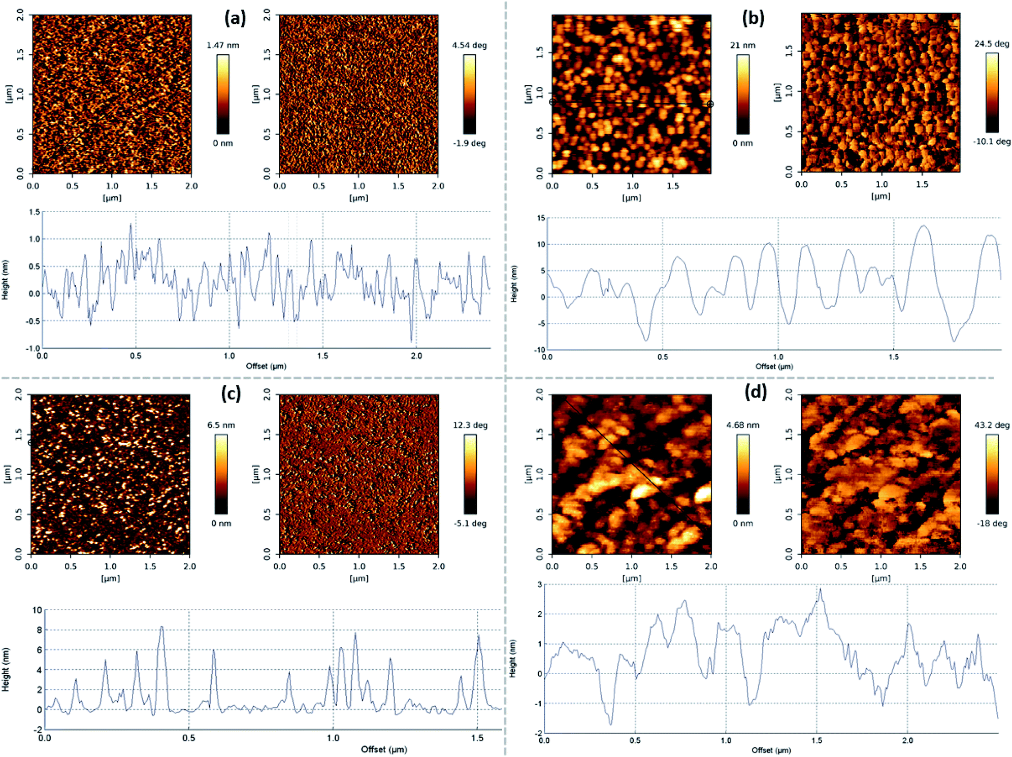 | ||
| Fig. 3 Typical graphene AFM images. The sample synthesis conditions: (a) plasma power, 0.7 kW; hydrogen flow, 150 sccm; methane flow, 50 sccm; pressure, 10 sccm; synthesis temperature, 700 °C; growth time, 50 min; (b) plasma power, 1.7 kW; hydrogen flow, 150 sccm; methane flow, 50 sccm; pressure, 22 mBar; synthesis temperature, 900 °C; growth time, 50 min; (c) plasma power, 0.7 kW; hydrogen flow, 75 sccm; methane flow, 25 sccm; pressure, 10 mBar; temperature, 900 °C; time, 50 min; (d) plasma power, 0.7 kW; hydrogen flow, 150 sccm; methane flow, 50 sccm; pressure, 22 mBar; temperature, 900 °C; time 50 min. | ||
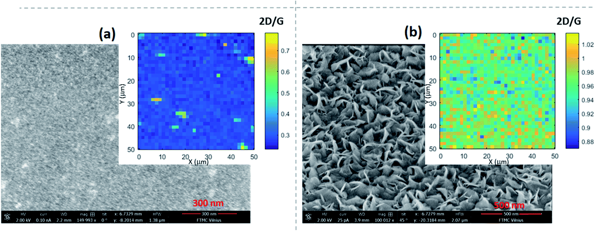 | ||
| Fig. 4 Typical graphene SEM images and I(2D)/I(G) mapping. The sample synthesis conditions: (a) plasma power, 0.7 kW; hydrogen flow, 75 sccm; methane flow, 35 sccm; pressure, 22 mBar; temperature, 700 °C; (b) plasma power, 1.7 kW; hydrogen flow, 150 sccm; methane flow, 50 sccm; pressure, 22 mBar; temperature, 900 °C; time, 90 min. | ||
The I(G)/I(Si) and I(2D)/I(G) ratios increased with the graphene roughness value (Rq) (Fig. 2b). Thus, based on the I(2D)/I(G) ratio, the sample roughness increases despite a decrease in the graphene layer number. This means that a graphene roughness increase is not related to a graphene layer number change. Taking into account Rq values above 5 nm, in this case, growth of non-planar graphene flakes can be supposed (Fig. 3 and 4). A thorough study of the graphene height histograms and AFM images of selected samples revealed that the samples with the lowest Rq values are planar graphene (Fig. 2b and 3a, S13–S15, S18, and S20†). In this case, the maximum feature height is 2–3 nm. Significant phase contrast was found for these low-roughness graphene layers (see, e.g., Fig. S12 and S13†), indicating the presence of different phases on the surfaces of the samples.49 Thus, some through-holes are present in the planar graphene layers. According to ref. 50 and 51, the graphene layer thickness is 0.41 nm. Thus, the maximum planar graphene thickness is 5–6 layers. No surface features can be seen in a typical SEM image measured for a sample from this group, indicating the growth of planar graphene (Fig. 4a). The Raman microscopy mapping study confirmed the deposition of graphene over the entire sample area (see the insets of Fig. 4a and b). Thus, the suppression of the Si-related peak is in good accordance with the increased sample roughness and non-planar graphene growth.
Samples with larger Rq values and with G/Si ratio values similar to planar graphene represent a mixture of planar and vertical graphene (Fig. 2). In this case, according to the height histograms, large proportions of the feature heights are within the range typical for planar few-layer graphene (Fig. 3c and d, and S11–S13, S16, and S18†). However, significant proportions of the heights are well beyond the thickness of ten graphene layers, despite the Raman spectra of the samples still being typical of graphene (Fig. 1b).
The last group of samples involves vertical graphene films. Their height histogram values are between several nm and several tens of nanometers (Fig. 3b, S4, S9, and S18–S20†). Vertical graphene flakes can be clearly observed in a typical SEM image (Fig. 4b). In this case, the presence of a mixture of bilayer and single-layer graphene can be supposed according to the I(2D)/I(G) ratio values of close to one.
Clarifying the analysis of the I(2D)/I(G) vs. I(G)/I(Si) graph, one can see that the first group of samples is made up of planar graphene and some planar graphene samples with the inclusion of non-planar graphene flakes (Fig. 2). The second group of samples is made up of mixed vertical and planar graphene samples and some vertical graphene samples. The third group is made up of vertical graphene samples only. This is related to the different graphene synthesis conditions. Most of the samples in group I are grown at a temperature of 700 °C using plasma power of 0.7 kW. However, all the samples in group III were synthesized at a temperature of 900 °C, plasma power of 1.7 kW, and with a synthesis time of at least 30 min. Therefore, the effects of the graphene synthesis conditions were then analyzed more thoroughly.
3.2 Synthesis condition effects
The technological parameters studied were plasma power, pressure, gas flows, temperature, and time. The electric field strength at the substrate surface increases with plasma power, promoting vertical graphene growth and potentially increasing the processing temperature.30 Lower pressure helps to achieve higher electron mean free paths and higher electron temperatures, subsequently increasing the gas ionization rate.18The carbon-containing active species flux at the surface promotes graphene growth.52 The graphene nucleus density decreases with an increased H2 content due to suppressed hydrogen etching, resulting in a smaller graphene grain size.53 A higher substrate temperature increases the temperature gradient and thermal stress, promoting the upward curling of graphene flakes and subsequent vertical graphene growth.18,54 Finally, the deposition time is important because the growth of vertical graphene begins with planar graphene growth.54 Then, due to stress, ion bombardment, and lattice mismatch between the substrate and graphene, vertical graphene growth begins.18,21,55
Via changing the gas flows, one can adjust the fluxes of active species, controlling the graphene growth52 and etching53 processes. Therefore, the gas-flow effects were also studied for necessary control of the graphene structure.
An analysis of AFM images revealed that for graphene synthesized at a temperature of 900 °C, a mixture of planar and vertical graphene was grown using plasma power in the range of 0.7–1.4 kW (Fig. S6–S9†). For all synthesized samples, graphene flakes with a width of 70–90 nm, length of 300 nm, and height of up to 4 nm are seen (Fig. S6–S9†). An increase in the plasma power to 1.7 kW resulted in the growth of vertical graphene flakes with a width of 60–80 nm (Fig. S5†). At the same time, the I(G)/I(Si) ratio and Rq value significantly increased (Fig. 5a and c). This can be explained because the electric field strength and ion bombardment increased with an increase in the plasma power, promoting vertical graphene growth.30 In contrast, possible plasma-induced temperature increase effects are somewhat limited (see Fig. S3†). At the same time, the I(2D)/I(G) ratio increased and the I(D)/I(G) ratio decreased with plasma power, indicating a lowering of the graphene layer number and defect density (Fig. 5e and g). The methane and hydrogen dissociation rates increase with plasma power.52 Thus, graphene etching by hydrogen prevailed over graphene growth, promoting increased C and CHx species densities.52,56 The decrease in defect density despite an increase in plasma power can be explained considering the prevailing defect types. For graphene synthesized using plasma power from 0.7 to 1.4 kW, boundary defects prevailed, and a further power increase resulted in the domination of boundary defects and vacancies (Fig. 5i). Thus, the I(D)/I(G) ratio decrease can be attributed to the increased graphene crystallite size. Increased ion irradiation can explain vacancy formation when using plasma power of 1.7 kW, as shown in numerous studies.57–62
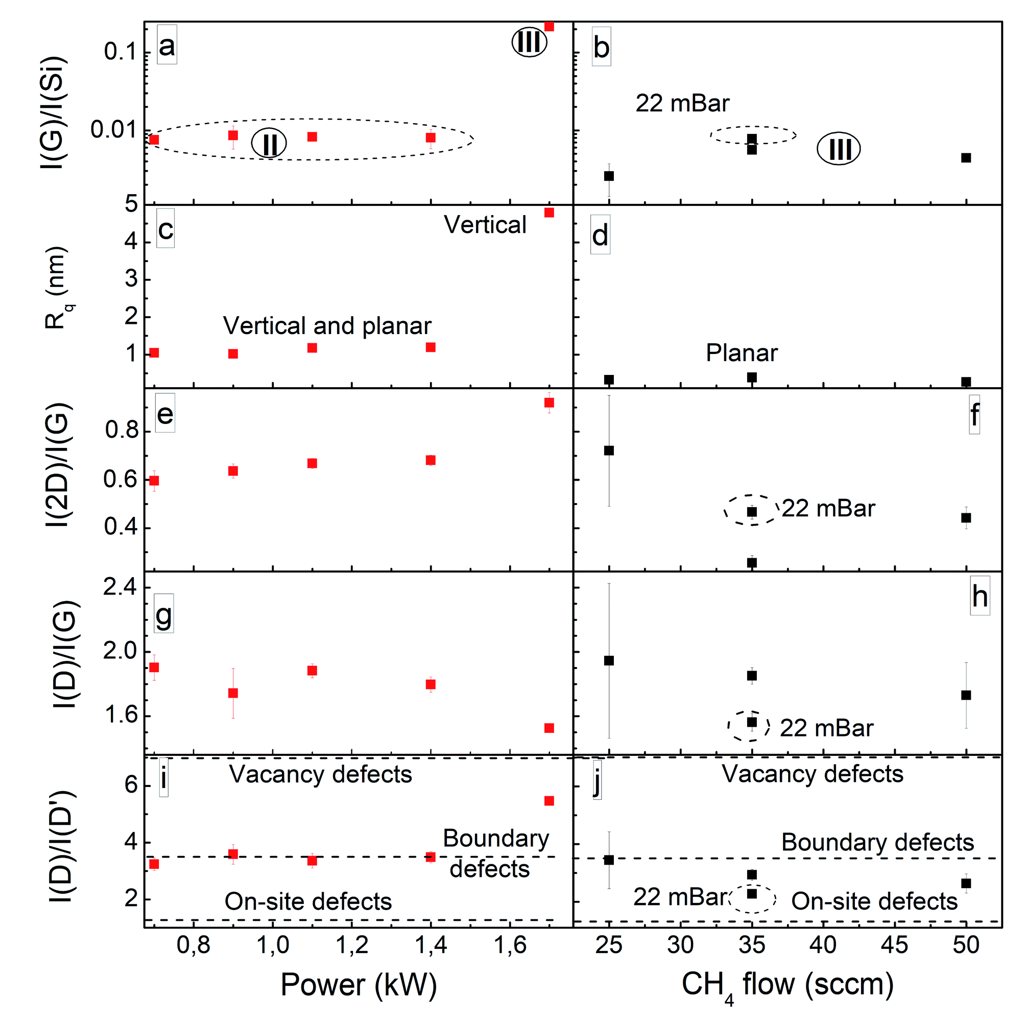 | ||
| Fig. 5 The effects of synthesis power (a, c, e, g, and i) and methane gas flow (b, d, f, h, and j) on the graphene structure: I(G)/I(Si) ratio (a and b); Rq (c and d); I(2D)/I(G) (e and f) and I(D)/I(G) ratios (g, h); and I(D)/I(D′) ratio (i and j). | ||
Doubling the processing pressure did not influence the graphene synthesized using a power of 1.7 kW (Fig. S4†). However, we achieved some control of the graphene layer number, defect density, and defect type for samples grown at 700 °C using power of 0.7 kW. Some on-site defects appeared along with boundary defects when the gas flows were increased (Fig. 5i). The presence of a more significant number of hydrocarbon species with a lower dissociation degree can be supposed.63 Synthesis pressure doubling slightly decreased the defect density and increased the layer number (Fig. 5g and h, S4†) due to the reduced gas ionization,18 resulting in lower ion etching and the formation of fewer radiative defects.
The synthesis temperature effects are shown in Fig. 6. It can be seen that no graphene was grown at 600 °C. In the synthesis temperature range of 700–900 °C, the I(G)/I(Si) and I(2D)/I(G) ratios increased with temperature when using a power of 1.7 kW for synthesis (Fig. 6a and e). When using power of 0.7 kW, the lowest graphene layer number was obtained at 800 °C. The graphene layer number changes are related to competition between decreased graphene etching by hydrogen53 and increased carbon atom desorption.64 The defect density slightly increased with temperature for graphene synthesized using power of 0.7 kW, while it non-monotonically depended on the temperature for graphene grown using power of 1.7 kW. The graphene Rq value increased with the synthesis temperature for all studied samples (Fig. 6c). The increased temperature promoted vertical graphene growth, activating the formation of non-planar graphene flakes along with planar ones, and the coverage of the entire sample surface with vertical graphene flakes occurred upon a further temperature increase (see Fig. S4, S13, S10, S14, S17, and S19–S22†). This can be explained based on the presence of higher temperature gradients and thermal stress, which promote the upward curling of graphene flakes and subsequent vertical graphene growth.18,54 The effects of temperature on the types of prevailing defects depended on the plasma power used for synthesis (Fig. 6i). For graphene synthesized using power of 1.7 kW, an increase in temperature resulted in the formation of vacancies along with boundary defects. Thus, additional thermal activation is necessary for ion-irradiation-induced vacancy formation.65
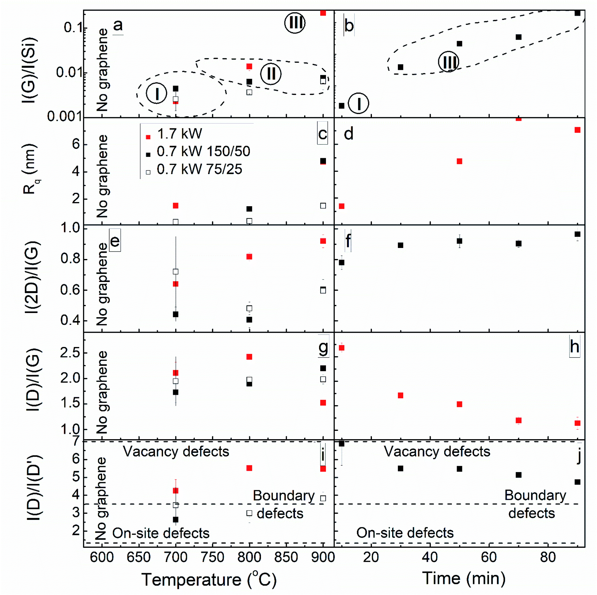 | ||
| Fig. 6 The dependence of the graphene structure on temperature (a, c, e, g and i) and time (b, d, f, h and j). | ||
The I(G)/I(Si) ratio and surface roughness significantly increased with the graphene synthesis time when a power of 1.7 kW and temperature of 900 °C were used for synthesis (Fig. 6b and d). After 10 min of growth, a planar and non-planar graphene mixture was formed. The I(G)/I(Si) ratio of that sample places it in group I, which mainly contains planar graphene. For the planar graphene areas, flakes with a height of 0.2–0.8 nm and a width of 15–25 nm were observed, and for non-planar graphene, flakes with a height of up to 5.5 nm and a width of 40–75 nm were seen (Fig. S22†). A further increase in the deposition time resulted in the growth of vertical graphene (Fig. S5 and S18–S20†). This follows the vertical graphene growth mechanism suggested in ref. 54. At first, planar graphene grows,54 and it is necessary for some time to elapse before vertical graphene growth begins due to thermal stress release.9,18,21,66 The I(2D)/I(G) ratio increased and the I(D)/I(G) ratio decreased with growth time for graphene deposited using power of 1.7 kW (Fig. 6f and h). The prevailing defect type changed from vacancy defects for graphene grown for 10 min to boundary defects for the sample synthesized for 90 min (Fig. 6j). The decrease in the graphene layer number with an increase in processing time can be explained based on the domination of hydrogen etching over additional graphene layer growth.64 The defect density decrease over time can be explained based on the self-annealing of vacancy defects59 and an increased graphene crystallite size.67
3.3 Graphene self-doping
The graphene FWHM(G), Pos(G), and Pos(2D) were analyzed to reveal possible doping and stress effects (Fig. 7). One can see the tendency of FWHM(G) to increase with an upshift in Pos(G) for the group III samples (Fig. 7a). This can be explained based on the increased defect density41 due to the decreased graphene crystallite size.67 Another tendency is for FWHM(G) to decrease with an upshift in Pos(G) for group I samples (Fig. 7a). That is typical of graphene doping effects.40–42 Thus, graphene self-doping can be suggested for group I samples.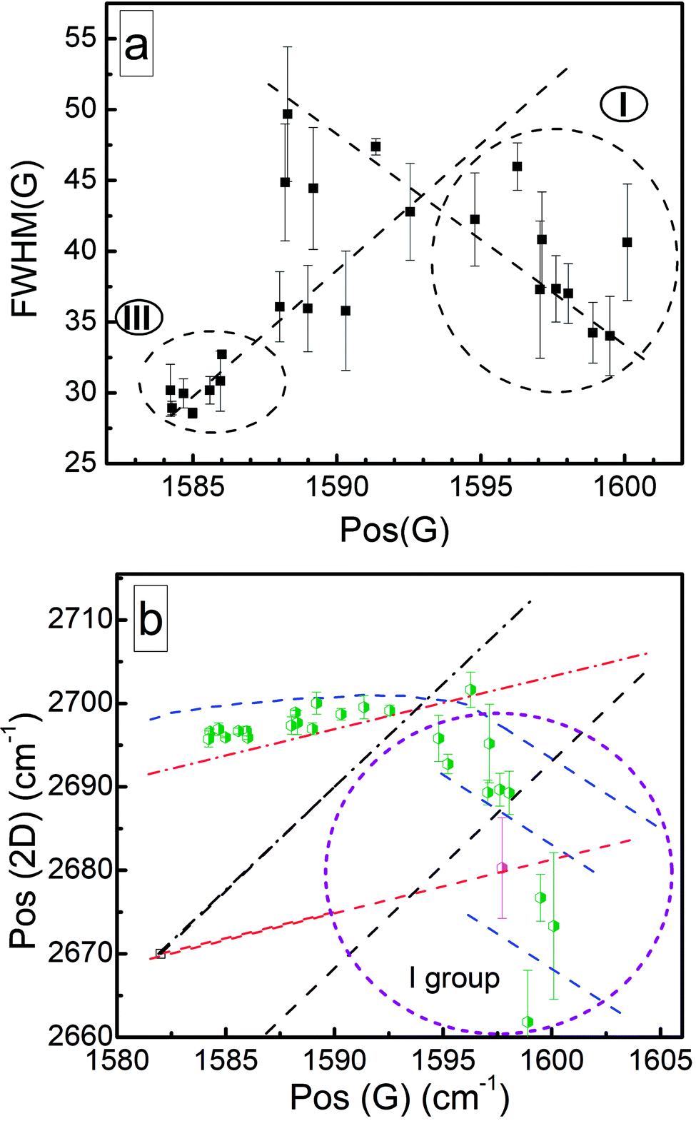 | ||
| Fig. 7 Plots of (a) FWHM(G) vs. Pos(G) and (b) Pos(2D) vs. Pos(G). In the Pos(2D) vs. Pos(G) plot, the black dashed-dotted line refers to undoped strained graphene (plotted according to the method in ref. 44). The black dotted line refers to p-type doped strained graphene (constant hole concentration and different stress levels) (plotted according to ref. 44). The red dotted line refers to unstrained p-type graphene (plotted according to ref. 44). The red dashed-dotted line refers to p-type doped strained graphene (constant stress level and different hole concentrations) (plotted according to the method in ref. 44). The blue dotted lines refer to n-type doped graphene (plotted according to ref. 44). The open square symbols refer to unstrained and undoped graphene.44 The green diamonds refer to the experimental points of graphene synthesized on n-type silicon substrates. The magenta-colored diamonds refer to the experimental points of graphene synthesized on p-type Si(100) (the synthesis conditions are the same as those for sample no. 12). | ||
Analysis of the Pos(2D) vs. Pos(G) plot revealed that for all group I samples, Pos(2D) is downshifted with an upshift in Pos(G) (Fig. 7b). This is typical of n-type doped graphene.36,40,42,44,45 For some samples, the Pos(2D) downshift with an upshift in Pos(G) was much more significant, and this could be explained only based on n-type self-doping (Fig. 7). The Pos(2D) downshift can occur due to a graphene layer number increase.47 However, in our case, no clear correlation between the large Pos(2D) downshift and I(2D)/I(G) ratio changes was found (Fig. S23†). Thus, a combination of n-type self-doping and stress effects can be suggested. Pos(2D) slightly upshifted with Pos(G) for other graphene samples (Fig. 7b). Thus, weak p-type doping can be supposed.40–42,44,45
Graphene self-doping has already been reported in numerous studies.36,68–74 In our case, n-type self-doping was found for all planar graphene samples and some samples consisting of a planar and non-planar graphene mixture. This is in accordance with the substrate-induced n-type self-doping hypothesis.71–74
Substrate-induced graphene n-type self-doping was reported for graphene placed on a SiO2 substrate due to positive silanol groups.75,76 It is noteworthy that a native oxide layer can be present at the interface between directly synthesized graphene and silicon due to silicon surface reoxidation.62 Thus, one can suppose that, in our case, electron transfer from the native silicon oxide interlayer to directly synthesized graphene takes place. The Pos(2D) vs. Pos(G) data for graphene synthesized on p-type Si(100) are in good accordance with this assumption (Fig. 7b and S24†).
For vertical graphene, most of the graphene surface is substrate-free.
Thus, charge transfer from the substrate to graphene is limited. However, a much larger graphene surface area is exposed to the air, and the adsorption of different ambient molecules is possible. This can induce p-type doping.68–70
4 Discussion and conclusions
The mechanisms causing the observed results can be generalized considering the effects of the technological conditions on the graphene structure and morphology and related physical and chemical processes. Vertical graphene growth is promoted by two main processes (Fig. 8).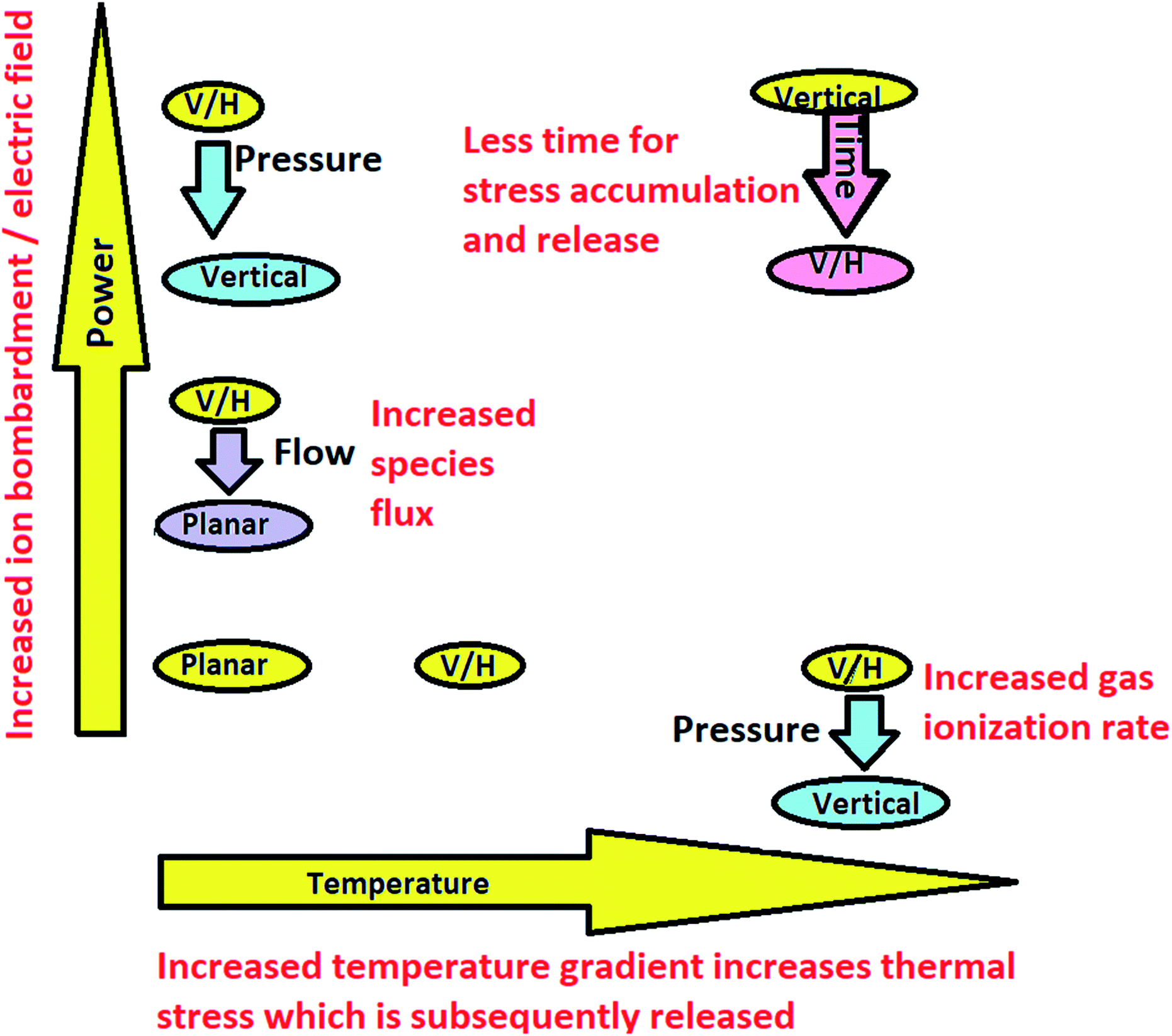 | ||
| Fig. 8 The dependence of the synthesized graphene flake orientation on the synthesis conditions. V/H refers to a vertical and planar graphene mixture. | ||
The temperature gradients and thermal stress increase with an increase in the synthesis temperature. At elevated temperatures, thermal stress is released by the partial detachment of graphene flakes from the substrate and curling. Some time is necessary for stress accumulation when the critical temperature is reached. In addition, it seems that the diffusion of radicals to the tops of vertical graphene flakes is more critical than the density of radicals on the surface.77 Another factor is ion bombardment and electric field effects,77 which are enhanced with an increase in plasma power.30 Ion bombardment generates surface defects and CHx radicals.77 If radicals are adsorbed on a defected flake edge, they can diffuse along the edge with a low probability of evaporation or transition to a side surface. The nanoflake sharp edges enhance the electric field, intensifying reactions due to ion focusing.77 Without the activation of these mechanisms, planar graphene grows.77 A decrease in pressure promotes vertical graphene growth due to increased gas ionization.18 This is, again, more important than the CHx radical density on the surface.77 The growth of planar graphene due to increased methane flow shows that an increased hydrocarbon species flux promotes planar graphene growth.
A decrease in the graphene layer number due to elevated temperature and a long synthesis time can be explained based on an increase in the carbon desorption rate with temperature.64 Thus, the vertical graphene flakes were thinner than the planar ones in most cases. Defect density changes should be analyzed, considering the presence of different defects. Notably, in most samples, boundary defects dominated. In the planar graphene samples, on-site defects can be formed. A low synthesis temperature, low power, and elevated methane flux may benefit their creation. Vacancies were found in samples containing vertical/planar graphene and vertical graphene. A combination of high power and increased temperature or a combination of low power with increased temperature and a longer growth time activated vacancy creation. Thus, carbon desorption and ion irradiation are essential processes.
In the case of planar graphene, n-type self-doping was revealed. This was explained based on charge transfer from the substrate. The growth of vertical graphene flakes resulted in a decreased contact area between the graphene flakes and the substrate. Therefore, charge transfer from the substrate was suppressed. In the case of vertical graphene, no doping or p-type doping was found. In this case, p-type doping can be explained based on an increased contact area between graphene and air, and more molecules can be adsorbed.
In conclusion, we were able to control the orientation of growing graphene flakes via adjusting the technological deposition process conditions. High temperature, high plasma power, and a prolonged synthesis time promoted vertical graphene growth due to increased temperature gradients, thermal stress, ion bombardment, and elevated electric field effects. Without these mechanisms, planar graphene grows at lower synthesis temperatures and lower plasma powers. The graphene layer number decreased with elevated temperatures and longer synthesis times because the carbon desorption rate increased with temperature. In most samples, boundary defects prevailed. A low synthesis temperature, low power, and elevated methane gas flow were beneficial for the formation of some on-site defects. Vacancy creation was activated by high plasma power, an increased growth temperature, and a shorter synthesis time. Substrate-based charge transfer resulted in planar graphene n-type self-doping. In the case of vertical graphene, no doping or p-type doping was found. The adsorption of more molecules can explain this, due to the increased contact area between graphene and air.
Author contributions
Š. Meškinis: conceptualization; visualization; writing – original draft; writing – review and editing; project administration; funding acquisition; A. Vasiliauskas: investigation; A. Guobienė: investigation; visualization; M. Talaikis: investigation; visualization; G. Niaura: investigation; writing – review and editing; R. Gudaitis: conceptualization; investigation.Conflicts of interest
The authors declare that they have no known competing financial interests or personal relationships that could have appeared to influence the work reported in this paper.Acknowledgements
Š. Meškinis, A. Vasiliauskas, A. Guobienė, and R. Gudaitis acknowledge the European Social Fund measure “Strengthening the Skills and Capacities of Public Sector Researchers for Engaging in High Level R&D Activities” administered by the Research Council of Lithuania with the research project no. 09.3.3-LMT-K-712-01-0183. The authors acknowledge other participants of the research project no. 09.3.3-LMT-K-712-01-0183 – M. Andrulevičius, A. Lazauskas, K. Šlapikas, V. Stankus, D. Peckus, E. Rajackaite, T. Tamulevičius, A. Jurkevičiūtė, Š. Jankauskas, and F. Kalyk. The authors acknowledge Dr A. Selskis for assistance with scanning electron microscopy measurements. The authors acknowledge the Center for Physical Sciences and Technology for allowing use of their scanning electron microscope and Raman microscope facilities.Notes and references
- T. Sattar, Current Review on Synthesis, Composites and Multifunctional Properties of Graphene, Top. Curr. Chem., 2019, 377, 10, DOI:10.1007/S41061-019-0235-6.
- L. Banszerus, M. Schmitz, S. Engels, J. Dauber, M. Oellers, F. Haupt and C. Stampfer, Ultrahigh-mobility graphene devices from chemical vapor deposition on reusable copper, Sci. Adv., 2015, 1, e1500222, DOI:10.1126/SCIADV.1500222.
- K. J. Tielrooij, J. C. W. Song, S. A. Jensen, A. Centeno, A. Pesquera, A. Zurutuza Elorza, M. Bonn, L. S. Levitov and F. H. L. Koppens, Photoexcitation cascade and multiple hot-carrier generation in graphene, Nat. Phys., 2013, 9(4), 248–252, DOI:10.1038/NPHYS2564.
- Z. H Khan, A. R. Kermany, A. Öchsner and F. Iacopi, Mechanical and electromechanical properties of graphene and their potential application in MEMS, J. Phys. D: Appl. Phys., 2017, 50, 053003, DOI:10.1088/1361-6463/50/5/053003.
- Y. Qi, B. Deng and X. Guo, et al., Switching Vertical to Horizontal Graphene Growth Using Faraday Cage-Assisted PECVD Approach for High-Performance Transparent Heating Device, Adv. Mater., 2018, 30, 1704839, DOI:10.1002/adma.201704839.
- Y. Zhang, L. Zhang and C. Zhou, Review of Chemical Vapor Deposition of Graphene and Related Applications, Acc. Chem. Res., 2013, 46, 2329–2339, DOI:10.1021/AR300203N.
- S. J. Haigh, A. Gholinia, R. Jalil, S. Romani, L. Britnell, D. C. Elias, K. S. Novoselov, L. A. Ponomarenko, A. K. Geim and R. Gorbachev, Cross-sectional Imaging of Individual Layers and Buried Interfaces of Graphene-Based Heterostructures and Superlattices, Nat. Mater., 2012, 11, 764–767, DOI:10.1038/NMAT3386.
- S. Deng and V. Berry, Wrinkled, rippled and crumpled graphene: an overview of formation mechanism, electronic properties, and applications, Mater. Today, 2016, 19, 197–212, DOI:10.1016/J.MATTOD.2015.10.002.
- M. Li, D. Liu, D. Wei, X. Song, D. Wei and A. T. S. Wee, Controllable Synthesis of Graphene by Plasma-Enhanced Chemical Vapor Deposition and Its Related Applications, Adv. Sci., 2016, 3, 1600003, DOI:10.1002/advs.201600003.
- O.-G. Simionescu, R.-C. Popa, A. Avram and G. Dinescu, Thin films of nanocrystalline graphene/graphite: An overview of synthesis and applications, Plasma Processes Polym., 2020, 17, 1900246, DOI:10.1002/ppap.201900246.
- S. Zheng, G. Zhong, X. Wu, L. D'Arsiè and J. Robertson, Metal-catalyst-free growth of graphene on insulating substrates by ammonia-assisted microwave plasma-enhanced chemical vapor deposition, RSC Adv., 2017, 7, 33185, 10.1039/c7ra04162d.
- O. Jašek, J. Toman, J. Jurmanová, M. Šnírer, V. Kudrle and V. Buršíková, Study of graphene layer growth on dielectric substrate in microwave plasma torch at atmospheric pressure, Diamond Relat. Mater., 2020, 105, 107798, DOI:10.1016/j.diamond.2020.107798.
- W.-S. Tseng, Y.-C. Chen, C.-C. Hsu, C.-H. Lu, C.-I. Wu and N.-C. Yeh, Direct large-area growth of graphene on silicon for potential ultra-low-friction applications and silicon-based technologies, Nanotechnology, 2020, 31, 335602, DOI:10.1088/1361-6528/ab9045.
- K. Ganesan, S. Ghosh, N. G. Krishna, S. Ilango, M. Kamruddina and A. K. Tyagi, A comparative study on defect estimation using XPS and Raman spectroscopy in few layer nanographitic structures, Phys. Chem. Chem. Phys., 2016, 18, 22160–22167, 10.1039/C6CP02033J.
- S. Ghosh, K. Ganesan, S. R. Polaki, S. Ilango, S. Amirthapandian, S. Dhara, M. Kamruddina and A. K. Tyagi, Flipping growth orientation of nanographitic structures by plasma enhanced chemical vapor deposition, RSC Adv., 2015, 5, 91922–91931, 10.1039/C5RA20820C.
- R. Vishwakarma, R. Zhu, A. A. Abuelwafa, Y. Mabuchi, S. Adhikari, S. Ichimura, T. Soga and M. Umeno, Direct Synthesis of Large-Area Graphene on Insulating Substrates at Low Temperature using Microwave Plasma CVD, Adv. Funct. Mater., 2012, 22, 2123–2128, DOI:10.1021/acsomega.9b00988.
- J. Hong, S. Lee and S. Lee, Graphene as an atomically thin barrier to Cu diffusion into Si, Nanoscale, 2014, 6, 7503–7511, 10.1039/C3NR06771H.
- Z. Bo, Y. Yang, J. Chen, K. Yu, J. Yan and K. Cen, Plasma-enhanced chemical vapor deposition synthesis of vertically oriented graphene nanosheets, Nanoscale, 2013, 5, 5180, 10.1039/c3nr33449j.
- K. Tanaka, M. Yoshimura, A. Okamoto and K. Ueda, Growth of Carbon Nanowalls on a SiO2 Substrate by Microwave Plasma-Enhanced Chemical Vapor Deposition, Jpn. J. Appl. Phys., 2005, 44, 2074, DOI:10.1143/JJAP.44.2074A11.
- L. Jiang, T. Yang, F. Liu, J. Dong, Z. Yao, C. Shen, S. Deng, N. Xu, Y. Liu and H.-J. Gao, Controlled Synthesis of Large-Scale, Uniform, Vertically Standing Graphene for High-Performance Field Emitters, Adv. Mater., 2013, 25, 250–255, DOI:10.1002/adma.201203902.
- M. Li, D. Liu, D. Wei, X. Song, D. Wei, A. Thye and S. Wee, Controllable Synthesis of Graphene by Plasma-Enhanced Chemical Vapor Deposition and Its Related Applications, Adv. Sci., 2016, 3, 1600003, DOI:10.1002/advs.201600003.
- Z. Zhang, C.-S. Lee and W. Zhang, Vertically Aligned Graphene Nanosheet Arrays: Synthesis, Properties and Applications in Electrochemical Energy Conversion and Storage, Adv. Energy Mater., 2017, 7, 1700678, DOI:10.1002/aenm.201700678.
- S. Y. Kim, S. K. Shin, H. Kim, Y.-H. Jung, H. Kang, W. S. Choi and G. B. Kweon, Synthesis of Carbon Nanowalls by Microwave PECVD for Battery Electrode, Trans. Electr. Electron. Mater., 2015, 16, 198–200, DOI:10.4313/TEEM.2015.16.4.198.
- J. J. Wang, M. Y. Zhu, R. A. Outlaw, X. Zhao, D. M. Manos, B. C. Holloway and V. P. Mammana, Free-standing subnanometer graphite sheets, Appl. Phys. Lett., 2004, 85, 1265, DOI:10.1063/1.1782253.
- J. Zhao, M. Shaygan, J. Eckert, M. Meyyappan and M. H. Rümmeli, A Growth Mechanism for Free-Standing Vertical Graphene, Nano Lett., 2014, 14, 3064–3071, DOI:10.1021/nl501039c.
- A. Vesel, R. Zaplotnik, G. Primc and M. Mozetič, Synthesis of Vertically Oriented Graphene Sheets or Carbon Nanowalls — Review and Challenges, Materials, 2019, 12, 2968, DOI:10.3390/ma12182968.
- H. Medina, Y.-C. Lin, C. Jin, C.-C. Lu, C.-H. Yeh, K.-P. Huang, K. Suenaga, J. Robertson and P.-W. Chiu, Metal-Free Growth of Nanographene on Silicon Oxides for Transparent Conducting Applications, Adv. Funct. Mater., 2012, 22, 2123–2128, DOI:10.1002/adfm.201102423.
- H. Chatei, M. Belmahi, M. B. Assouar, L. Le Brizoual, P. Bourson and J. Bougdira, Growth and characterisation of carbon nanostructures obtained by MPACVD system using CH4/CO2 gas mixture, Diamond Relat. Mater., 2006, 15, 1041–1046, DOI:10.1016/j.diamond.2005.10.025.
- M. Ye. Svavil’nyi, V. Ye. Panarin, A. A. Shkola, A. S. Nikolenko and V. V. Strelchuk, Plasma Enhanced Chemical Vapor Deposition synthesis of graphene-like structures from plasma state of CO2 gas, Carbon, 2020, 167(15), 132–139, DOI:10.1016/j.carbon.2020.05.057.
- N. M. Santhosh, G. Filipič, E. Tatarova, O. Baranov, H. Kondo, M. Sekine, M. Hori, K. (Ken) Ostrikov and U. Cvelbar, Oriented Carbon Nanostructures by Plasma Processing- Recent Advances and Future Challenges, Micromachines, 2018, 9, 565, DOI:10.3390/mi9110565.
- R. Spitzl, B. Aschermann and M. Walter, Microwave plasma generator with the short cross-sectional side of the resonator parallel to the chamber axis, US Pat. 6198224, 2001.
- H. Sung-Spitzl, Device for the production of homogenous microwave plasma, WO1998059359A1, 1998.
- J. Engemann and M. Walter, Modelling of microwave plasma sources: potential and applications, Plasma Phys. Controlled Fusion, 1999, 41, B259 CrossRef CAS.
- V. Hopfe, R. Spitzl, I. Dani, G. Maeder, L. Roch, D. Rogler, B. Leupolt and B. Schoeneich, Remote Microwave PECVD for Continuous, Wide-Area Coating Under Atmospheric Pressure, Chem. Vap. Deposition, 2005, 11, 497–509, DOI:10.1002/cvde.200406352.
- A. Pfuch and R. Cihar, Deposition of SiOx thin films by microwave induced plasma CVD at atmospheric pressure, Surf. Coat. Technol., 2004, 183, 134–140, DOI:10.1016/j.surfcoat.2003.09.052.
- R. Gudaitis, A. Lazauskas, Š. Jankauskas and Š. Meškinis, Catalyst-Less and Transfer-Less Synthesis of Graphene on Si(100) Using Direct Microwave Plasma Enhanced Chemical Vapor Deposition and Protective Enclosures, Materials, 2020, 13(24), 5630, DOI:10.3390/ma13245630.
- J.-S. Hwang, Y.-H. Lin, J.-Y. Hwang, R. Chang, S. Chattopadhyay, C.-J. Chen, P. Chen, H.-P. Chiang, T.-R. Tsai and L.-C. Chen, Imaging layer number and stacking order through formulating Raman fingerprints obtained from hexagonal single crystals of few layer graphene, Nanotechnology, 2012, 24, 015702, DOI:10.1088/0957-4484/24/1/015702.
- I. Childres, L. A. Jauregui, J. Tian and Y. P. Chen, Effect of oxygen plasma etching on graphene studied using Raman spectroscopy and electronic transport measurements, New J. Phys., 2011, 13, 025008, DOI:10.1088/1367-2630/13/2/025008.
- M. S. Dresselhaus, A. Jorio, A. G. Souza Filho and R. Saito, Defect characterization in graphene and carbon nanotubes using Raman spectroscopy, Philos. Trans. R. Soc., A, 2010, 368, 5355–5377, DOI:10.1098/rsta.2010.0213.
- A. Das, S. Pisana, B. Chakraborty, S. Piscanec, S. K. Saha and U. V. Waghmare, et al., Monitoring dopants by Raman scattering in an electrochemically top-gated graphene transistor, Nat. Nanotechnol., 2008, 3(4), 210–215, DOI:10.1038/nnano.2008.67.
- C. Casiraghi, Probing disorder and charged impurities in graphene by Raman spectroscopy, Phys. Status Solidi RRL, 2009, 3, 175–177, DOI:10.1002/pssr.200903135.
- J. H. Bong, O. Sul, A. Yoon, S.-Y. Choi and B. J. Cho, Facile graphene n-doping by wet chemical treatment for electronic applications, Nanoscale, 2014, 6, 8503–8508 RSC , https://pubs.rsc.org/en/content/articlelanding/2014/NR/C4NR01160K.
- A. Eckmann, A. Felten, A. Mishchenko, L. Britnell, R. Krupke, K. S. Novoselov and C. Casiraghi, Probing the Nature of Defects in Graphene by Raman Spectroscopy, Nano Lett., 2012, 12, 3925–3930, DOI:10.1021/nl300901a.
- J. E. Lee, G. Ahn, J. Shim, Y. S. Lee and S. Ryu, Optical separation of mechanical strain from charge doping in graphene, Nat. Commun., 2012, 3, 1024, DOI:10.1038/ncomms2022.
- A. Sakavičius, G. Astromskas, V. Bukauskas, M. Kamarauskas, A. Lukša, V. Nargelienė, G. Niaura, I. Ignatjev, M. Treideris and A. Šetkus, Long distance distortions in the graphene near the edge of planar metal contacts, Thin Solid Films, 2020, 698, 137850, DOI:10.1016/j.tsf.2020.137850.
- X.-L. Li, X.-F. Qiao, W.-P. Han, Y. Lu, Q.-H. Tan, X.-L. Liu and P.-H. Tan, Layer number identification of intrinsic and defective multilayered graphenes up to 100 layers by the Raman mode intensity from substrates, Nanoscale, 2015, 7, 8135–8141, 10.1039/C5NR01514F.
- J.-S. Hwang, Y.-H. Lin, J.-Y. Hwang, R. Chang, S. Chattopadhyay, C.-J. Chen, P. Chen, H.-P. Chiang, T.-R. Tsai and L.-C. Chen, Imaging layer number and stacking order through formulating Raman fingerprints obtained from hexagonal single crystals of few layer graphene, Nanotechnology, 2012, 24, 015702, DOI:10.1088/0957-4484/24/1/015702.
- A. F. Qian, J. Deng, F. Xiong, Y. Dong, L. Hu, G. Pan, Q. Wang, Y. Xie, J. Sun and C. Xu, Direct growth of high quality graphene nanowalls on dielectric surfaces by plasma-enhanced chemical vapor deposition for photo detection, Opt. Mater. Express, 2020, 10, 2909–2918, DOI:10.1364/OME.404881.
- Z. Osváth, E. Gergely-Fülöp, N. Nagy, A. Deák, P. Nemes-Incze, X. Jin, C. Hwang and L. P. Biró, Controlling the nanoscale rippling of graphene with SiO2 nanoparticles, Nanoscale, 2014, 6, 6030–6036, 10.1039/C3NR06885D.
- Y. Yaxuan, R. Lingling, G. Sitian and L. Shi, Histogram method for reliable thickness measurements of graphene films using atomic force microscopy (AFM), J. Mater. Sci. Technol., 2017, 33, 815–820, DOI:10.1016/j.jmst.2016.07.020.
- C. J. Shearer, A. D. Slattery, A. J. Stapleton, J. G. Shapter and C. T. Gibson, Accurate thickness measurement of graphene, Nanotechnology, 2016, 27, 125704, DOI:10.1088/0957-4484/27/12/125704.
- Y. S. Kim, K. Joo, S.-K. Jerng, J. H. Lee, E. Yoon and S.-H. Chun, Direct growth of patterned graphene on SiO2 substrates without the use of catalysts or Lithography, Nanoscale, 2014, 6, 10100, 10.1039/C4NR02001D.
- R. Muñoz, C. Munuera, J. I. Martínez, J. Azpeitia, C. Gómez-Aleixandre and M. García-Hernández, Low temperature metal free growth of graphene on insulating substrates by plasma assisted chemical vapor deposition, 2D Mater., 2017, 4, 015009, DOI:10.1088/2053-1583/4/1/015009.
- N. Soin, S. S. Roy, Ch. O'Kane, J. A. D. McLaughlin, T. H. Lim and C. J. D. Hetherington, Exploring the fundamental effects of deposition time on the microstructure of graphene nanoflakes by Raman scattering and X-ray diffraction, CrystEngComm, 2011, 13, 312–318, 10.1039/C0CE00285B.
- M. Li, D. Liu, D. Wei, X. Song, D. Wei and A. T. S. Wee, Controllable Synthesis of Graphene by Plasma-Enhanced Chemical Vapor Deposition and Its Related Applications, Adv. Sci., 2016, 3, 1600003, DOI:10.1002/advs.201600003.
- I. Vlassiouk, et al., Role of Hydrogen in Chemical Vapor Deposition Growth of Large Single-Crystal Graphene, ACS Nano, 2011, 5(7), 6069–6076, DOI:10.1021/nn201978y.
- A. Zandiatashbar, G. H. Lee and S. An, et al., Effect of defects on the intrinsic strength and stiffness of graphene, Nat. Commun., 2014, 5, 3186, DOI:10.1038/ncomms4186.
- C. Lin, K. Davami, Y. Jiang, J. Cortes, M. Munther, M. Shaygan, H. Ghassemi, J. T Robinson, K. T Turner and I. Bargatin, Enhancing the stiffness of vertical graphene sheets through ion beam irradiation and fluorination, Nanotechnology, 2017, 28, 295701, DOI:10.1088/1361-6528/aa75ac.
- L. Liu, M. Qing, Y. Wang and S. Chen, Defects in Graphene: Generation, Healing, and Their Effects on the Properties of Graphene. A Review, J. Mater. Sci. Technol., 2015, 31(6), 599–606, DOI:10.1016/j.jmst.2014.11.019.
- S. He, W. Xie, Y. Zhang, S. Fang, D. Zhou, J. Gan, Z. Zhang, J. Du, C. Du and D. Wang, Probing the Influence of the Substrate Hole Shape on the Interaction between Helium Ions and Suspended Monolayer Graphene with Raman Spectroscopy, J. Phys. Chem. C, 2021, 125(3), 2202–2211, DOI:10.1021/acs.jpcc.0c10738.
- J. Martinez-Asencio, C. J. Ruestes, E. M. Bringa and M. J. Caturla, Controlled rippling of graphene via irradiation and applied strain modify its mechanical properties: a nanoindentation simulation study, Phys. Chem. Chem. Phys., 2016, 18, 13897–13903, 10.1039/C6CP01487A.
- A. Eckmann, A. Felten, A. Mishchenko, L. Britnell, R. Krupke, K. S. Novoselov and C. Casiraghi, Probing the Nature of Defects in Graphene by Raman Spectroscopy, Nano Lett., 2012, 12(8), 3925–3930, DOI:10.1021/nl300901a.
- K. Jia, J. Zhang, L. Lin, Z. Li, J. Gao, L. Sun, R. Xue, J. Li, N. Kang, Z. Luo, M. H. Rummeli, H. Peng and Z. Liu, Copper-containing carbon feedstock for growing superclean graphene, J. Am. Chem. Soc., 2019, 141, 7670–7674, DOI:10.1021/JACS.9B02068.
- S. Chaitoglou and E. Bertran, Effect of temperature on graphene grown by chemical vapor deposition, J. Mater. Sci., 2017, 52, 8348–8356, DOI:10.1007/s10853-017-1054-1.
- Z. Luo, T. Yu, K. Kim, Z. Ni, Y. You, S. Lim, Z. Shen, S. Wang and J. Lin, Thickness-Dependent Reversible Hydrogenation of Graphene Layers, ACS Nano, 2009, 3, 1781–1788, DOI:10.1021/nn900371t.
- S. Xu, S. Wang, Z. Chen, Y. Sun, Z. Gao, H. Zhang and J. Zhang, Electric-Field-Assisted Growth of Vertical Graphene Arrays and the Application in Thermal Interface Materials, Adv. Funct. Mater., 2020, 30, 2003302, DOI:10.1002/adfm.202003302.
- P. Mallet-Ladeira, et al., A Raman study to obtain crystallite size of carbon materials: A better alternative to the Tuinstra–Koenig law, Carbon, 2014, 80, 629–639, DOI:10.1016/j.carbon.2014.09.006.
- S. Ryu, L. Liu, S. Berciaud, Y.-J. Yu, H. Liu, P. Kim, G. W. Flynn and L. E. Brus, Atmospheric Oxygen Binding and Hole Doping in Deformed Graphene on a SiO2 Substrate, Nano Lett., 2010, 10(12), 4944–4951, DOI:10.1021/nl1029607.
- C. Casiraghi, S. Pisana, K. S. Novoselov, A. K. Geim and A. C. Ferrari, Raman fingerprint of charged impurities in graphene, Appl. Phys. Lett., 2007, 91, 233108, DOI:10.1063/1.2818692.
- E. A. Kolesov, M. S. Tivanov, O. V. Korolik, O. O. Kapitanova, X. Fu, H.-D. Cho, T.-W. Kang and G. N. Panin, The effect of atmospheric doping on pressure-dependent Raman scattering in supported graphene, Beilstein J. Nanotechnol., 2018, 9, 704–710, DOI:10.3762/bjnano.9.65.
- J. Eriksson, D. Puglisi, R. Vasiliauskas, A. Lloyd Spetz and R. Yakimova, Thickness uniformity and electron doping in epitaxial graphene on SiC, Mater. Sci. Forum, 2013, 740–742, 153–156, DOI:10.4028/www.scientific.net/MSF.740-742.153.
- H.-G. Jee, K.-H. Jin, J.-H. Han, H.-N. Hwang, S.-H. Jhi, Y. D. Kim and C.-C. Hwang, Controlling the self-doping of epitaxial graphene on SiC via Ar ion treatment, Phys. Rev. B, 2011, 84, 075457, DOI:10.1103/PhysRevB.84.075457.
- L. Banszerus, H. Janssen, M. Otto, A. Epping, T. Taniguchi, K. Watanabe, B. Beschoten, D. Neumaier and C. Stampfer, Identifying suitable substrates for high-quality graphene-based heterostructures, 2D Mater., 2017, 4, 025030, DOI:10.1088/2053-1583/aa5b0f.
- Y.-J. Kang, J. Kang and K. J. Chang, Electronic structure of graphene and doping effect on SiO2, Phys. Rev. B, 2008, 78, 115404, DOI:10.1103/PhysRevB.78.115404.
- S. Wittmann, F. Aumer, D. Wittmann, S. Pindl, S. Wagner, A. Gahoi, E. Reato, M. Belete, S. Kataria and M. C. Lemme, Dielectric Surface Charge Engineering for Electrostatic Doping of Graphene, ACS Appl. Electron. Mater., 2020, 2, 1235–1242 CrossRef CAS.
- Y. Shi, X. Dong, P. Chen, J. Wang and L.-J. Li, Effective Doping of Single-Layer Graphene from Underlying SiO2, Phys. Rev. B, 2009, 79, 115402 CrossRef.
- O. Baranov, I. Levchenko, S. Xu, J. W. M. Lim, U. Cvelbar and K. Bazaka, Formation of vertically oriented graphenes: what are the key drivers of growth?, 2D Mater., 2018, 5, 044002 CrossRef CAS.
Footnote |
| † Electronic supplementary information (ESI) available. See https://doi.org/10.1039/d2ra02370a |
| This journal is © The Royal Society of Chemistry 2022 |