
 Open Access Article
 This Open Access Article is licensed under a Creative Commons Attribution-Non Commercial 3.0 Unported Licence
Impact of rare earth (RE3+ = La3+, Sm3+) substitution in the A site perovskite on the structural, and electrical properties of Ba(Zr0.9Ti0.1)O3 ceramics†
Amine Bendahhou *,
Karim Chourti,
Mohamed Loutou,
Soufian El Barkany and
Mohamed Abou-Salama
*,
Karim Chourti,
Mohamed Loutou,
Soufian El Barkany and
Mohamed Abou-Salama
Laboratory of Molecular Chemistry, Materials and Environment, Department of Chemistry, Faculty Multidisciplinary Nador, University Mohamed Premier, B. P. 300, Selouane, Nador 62700, Morocco. E-mail: bendahhou_amine1718@ump.ac.ma; Tel: +212 606849738
First published on 7th April 2022
Abstract
Undoped Ba(Zr0.9Ti0.1)O3 and rare-earth-doped (Ba1−xRE2x/3)(Zr0.9Ti0.1)O3 (RE3+ = La3+, Sm3+) perovskite compounds were synthesized by the conventional solid-state reaction route. Both solubility of rare earth in Ba(Zr0.9Ti0.1)O3 and formation of perovskite structure with the Pm![[3 with combining macron]](https://www.rsc.org/images/entities/char_0033_0304.gif) m space group were verified by the Rietveld method using X-ray diffraction data. SEM micrographs of all ceramics revealed high densification, low porosity, and even homogeneous grain distribution of various dimensions over the total surface. The frequency-dependent electrical properties were analyzed by complex impedance spectroscopy. Different types of studies such as the Nyquist plot, real and imaginary part of impedance, conductivity, modulus formalism, and charge carriers activation energy were used to explain the microstructure–electrical property relationships.
m space group were verified by the Rietveld method using X-ray diffraction data. SEM micrographs of all ceramics revealed high densification, low porosity, and even homogeneous grain distribution of various dimensions over the total surface. The frequency-dependent electrical properties were analyzed by complex impedance spectroscopy. Different types of studies such as the Nyquist plot, real and imaginary part of impedance, conductivity, modulus formalism, and charge carriers activation energy were used to explain the microstructure–electrical property relationships.
1. Introduction
In recent decades, components in electronic equipment became more and more sophisticated to satisfy the requirements of emerging technologies. From the literature study, various materials have been explored.1,2 In addition, perovskite materials are the most attractive candidates for low-cost electronic components because of their easy fabrication and extensive functional properties.3–7 Simple perovskite-type oxides with the general chemical formula ABO3 (A and B indicating cations) have been extensively investigated for their significant structural, chemical and physical properties such as optical, thermal, catalytic, dielectric, electrical, electronic and magnetic properties.8–10 Since the 1940s, perovskite materials of different structural families have been widely used in various applications such as capacitors, memory, photocatalysts, gas sensors, cathodes for fuel cells, photoluminescent materials, spintronic devices, etc.11,12 Moreover, perovskites are known to accept multiple substitutions at the A and B sites. As a result, there are three distinct families of complex perovskites, A1−xA′xBO3, AB1−xB′xO3 and A1−xA′xB1−yB′yO3.Unfortunately, some lead-based perovskite oxides, such as lead titanate (PbTiO3), lead magnesium niobate (Pb(Mg1/3Nb2/3)O3), lead zirconate titanate (Pb(Zr, Ti)O3), etc., exhibit a large spontaneous polarization, high dielectric constant and low tangent loss. Consequently, they are applied for different electronic devices, such as multilayer capacitor, pyroelectric detector, actuators, etc.13–15 Currently, the commercial production and applications of Pb (lead) based compounds have become a serious problem for achieving a clean and healthy environment due to their toxicity. In this regard, a universal industrial restriction has recently been adopted regarding the use of toxic materials.16 Therefore, the need to develop materials which are both efficient and environmentally friendly has become an important alternative that is attracting a lot of attention. For example, Ba(ZrxTi1−x)O3 (BZT) based ceramics have received a lot of attention for many decades due to their excellent dielectric, ferroelectric, electromechanical and piezoelectric properties.17,18 They are known to be environmentally friendly lead-free ferroelectrics with potential applications implying multilayer ceramic capacitors, tunable microwave devices, piezoelectric actuators, etc.19–22 In general, the properties of these materials are mostly associated with the significant changes in electrical and structural properties, created by the partial replacement of Ti4+ by Zr4+ in the BZT structure. In addition, the Zr4+ ion is chemically more stable than Ti4+ and has a larger ionic size, which increases the lattice of the perovskite. Hence, replacing Ti4+ with Zr4+ would reduce the electron hopping conduction between Ti4+ and Ti3+ and also decrease the leakage current of the BaTiO3 system. Recently, new emerging applications of BZT-based compounds, such as electrocaloric cooling systems or energy storage capacitors, have received a large number of publications.23–32 Doping in BZT ceramics has become a popular way to enhance the performance of the material.33–37 The dopant inserted into the BZT plays a crucial role in compensating the defects created in the perovskite structure. The dopant can be an acceptor or a donor and, therefore, requires oxygen vacancies or holes and electrons or barium vacancies, respectively for defect compensation.36,38 The isovalent dopants do not influence the defect sites but the anisovalent dopants have an extensive effect on the defect and need a defect compensation for the charge neutrality. The rare earth ions (RE3+), due to their moderate ionic radii and ability to replace the A and B site atoms in the perovskite structure are largely used to enhance the electrical and optical properties of the BZT system.39–45 The ionic radii of these trivalent elements are between 0.8 and 1.3 Å, which is in between the ionic radii of Ba2+ and Ti4+/Zr4+ ions. According to the ionic radii, these ions can replace atoms in the A site (Ba1−xRE2x/3TiO3) or the B site (BaTi1−xRExO3−x/2). Nevertheless, the intermediate ions can be substituted on the A and B sites in equal quantities (self-compensation, Ba1−xRExTi1−xRExO3).46 Therefore, the incorporation of any dopant ion (RE3+) into the BZT structure depends on three important factors: (1) the crystallographic site where the dopant is incorporated, (2) the mechanism of charge compensation and, (3) the Ba/Ti concentration ratio.47 It is well known that the microstructural and electrical properties of perovskite materials depend on the sites preferred by trivalent ions and the properties of the material can be enhanced by rare earths doping.48
In recent years, a lot of research has focused on enhancing the electrical properties of BZT by substitutions, investigate impedance data in order to identify the contribution of bulk (grains) and grain boundary effects, determine which elements are responsible for the conduction phenomenon in BZT ceramics at high temperature. The researchers observed that changing the MgO concentration has a significant effect on the electrical properties of Ba(Zr0.15Ti0.85)O3 ceramics, the electrical resistance of the co-doped samples showed a strong dependence on grain size, which resulted in a reduced resistivity compared to BaTiO3 ceramics.49 The introduction of lanthanum into the A-site perovskite shows that with the addition of La3+ in the B0.9Ca0.1Ti0.9Zr0.1O3 system, there is a decrease in the number of oxygen vacancies.50 Chandra Das et al. reported that for Ba0.985Sr0.015Zr0.10Ti0.90O3 ceramics, the equivalent circuit utilized to describe the electrical properties of the material is composed of two branches in series, which represent the electrical properties of the grain and grain boundary, and the values of Rg and Rgb decrease with an increase in temperature, which establishes the NTCR nature of the compound BSZT.51 Ismail et al. have demonstrated that the permittivity value varied from 4000 to 19![[thin space (1/6-em)]](https://www.rsc.org/images/entities/char_2009.gif) 000 with increasing doping concentration for the different types of RE dopants (Ce, La, Sm, Nd, Er), and indicated that Er-doped BTO exhibited the highest value, i.e., 19000, for only 1% Er3+ content.52 The present work is focused on the rare earths (RE3+ = La3+, Sm3+) substitution in the A site perovskite, for compounds of global composition (Ba0.9RE0.067)(Zr0.9Ti0.1)O3 (RE3+ = La3+ and Sm3+) synthesized by standard solid-state reaction. The aims of the present work are: (i) to study the structural modifications induced by rare earths substitution, (ii) to investigate the dielectric properties of ceramics samples (relative permittivity, dielectric losses, conductivity, relaxation phenomena) in order to understand the relationships between structure, and properties.
000 with increasing doping concentration for the different types of RE dopants (Ce, La, Sm, Nd, Er), and indicated that Er-doped BTO exhibited the highest value, i.e., 19000, for only 1% Er3+ content.52 The present work is focused on the rare earths (RE3+ = La3+, Sm3+) substitution in the A site perovskite, for compounds of global composition (Ba0.9RE0.067)(Zr0.9Ti0.1)O3 (RE3+ = La3+ and Sm3+) synthesized by standard solid-state reaction. The aims of the present work are: (i) to study the structural modifications induced by rare earths substitution, (ii) to investigate the dielectric properties of ceramics samples (relative permittivity, dielectric losses, conductivity, relaxation phenomena) in order to understand the relationships between structure, and properties.
The choice of these trivalent rare earths (RE3+ = La3+ and Sm3+) is justified by their particular electronic configuration that can lead to specific behaviors. In fact, the trivalent ions RE3+ behave as a donor by replacing Ba2+ ions in BZT compounds, which leads to a charge imbalance, which promotes the improvement of the properties of BZT ceramics.
2. Background
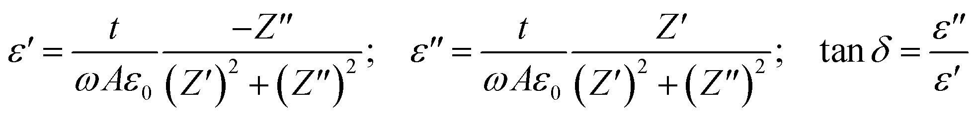
The complex impedance spectroscopy (CIS) technique has been extensively used to study the physical processes determining the electrical and dielectric properties of materials. It is used to separate the contributions of grains and grain boundaries to the transport properties of materials.53 The variation of impedance parameters as a function of frequency and temperature can be appropriately modelled with equivalent circuits, which will assist the researcher in determining the responsible physical processes.54–58 CIS allows the study of conductivity as a function of frequency, modulus spectra, relative permittivity and dielectric losses. The terms are expressed as follows,
 | (1) |
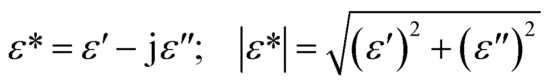
In this study, the relative permittivity (dielectric constant ε′) and the dielectric losses (tanδ) were determined from complex impedance Z* data (Z* = Z′ + jZ′′) using the following expressions:59
 | (2) |
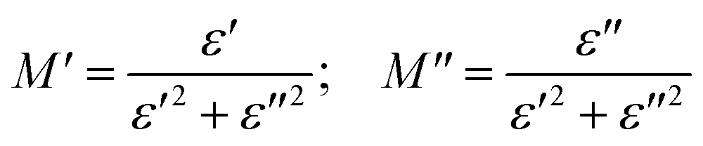
The electrical properties of the materials are analyzed in terms of complex modulus analysis to magnify the dynamic aspects such as AC and DC conductivity, hopping mechanism, etc. present in the sample. The complex modulus can be described as follows
| M* = 1/ε* = jωC0Z* = M′ + jM′′ | (3) |
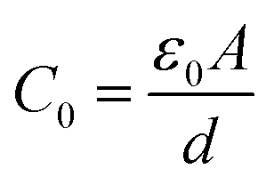 is the geometric capacitance (where ε0 = vacuum permittivity, A = surface, d = thickness).
The real and imaginary parts of the complex module are expressed as following:
 | (4) |
3. Materials and methods
Ba(Zr0.9Ti0.1)O3, (Ba0.9La0.067)(Zr0.9Ti0.1)O3 and (Ba0.9Sm0.067)(Zr0.9Ti0.1)O3 powders (denoted as BZT, BLaZT and BSmZT, respectively) were prepared by conventional high temperature solid state processing. High purity BaCO3, La2O3, Sm2O3, ZrO2 and TiO2 were used as starting materials. The rare earth oxides were heated at 850 °C for 2 h before weighing. The materials were weighed in stoichiometric amounts according to the reaction below and mixed by ball milling in ethanol for 1 h using zirconia balls.
The wet mixtures were then dried at 100 °C for 12 h and calcined at 1350 °C, 6 h in air. After being ground and dried again, 6 wt% polyvinyl alcohol (PVA) was added to the resulting powder and then pressed into the mold (12 mm diameter and 2 mm thickness). Finally, in order to remove the binder, the green pellets were held at 700 °C for 1 hour and then sintered at 1450 °C for 6 hours in air. After the sintering process, the experimental densities of the prepared ceramics were measured by the Archimedes method.
The identification of the crystalline structure of the powders was performed by X-ray diffraction (XRD) using a θ/2θ diffractometer fitted with a fast detector (Bruker D8, CuKα1, Linkeye detector) at room temperature (293 K, 0.015° per step, 10–120° 2θ range, scanning speed of 1° min−1). The lattice parameters, atomic positions, occupation rates, and thermal agitation factors were refined by the Rietveld method using the Jana 2006 software.60 The crystallite size “D” was estimated for the strongest diffraction peak using the Scherrer equation.61 Before electrical measurements, the sintered ceramic was painted with a silver paste and annealed for 30 minutes at 300 °C to adhere the silver paste on the sample and then cooled to room temperature before taking any measurement. The relative permittivity, dielectric losses (tanδ), the real and imaginary part of impedance and phase angle were determined using a BioLogic impedance analyzer (MTZ-35) over the frequency range of 10 Hz to 1 MHz.
4. Results and discussion
4.1 Structural study
The X-ray diffraction (XRD) plots of the BZT, BLaZT and BSmZT powders registered at room temperature in the 2θ range varying between 20 and 80° are shown in Fig. 1a. All the samples have a perovskite structure and no second phase can be detected, indicating that (RE3+ = La3+, Sm3+) has diffused into the structure to form a solid solution in which RE3+ = La3+, Sm3+ occupies the A site of the perovskite structure.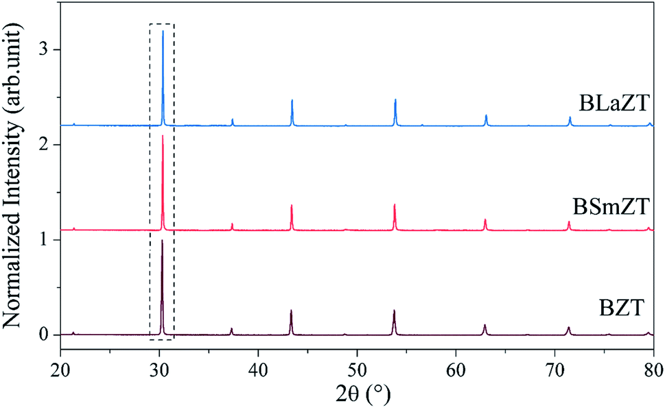 | ||
| Fig. 1 XRD diffraction diagrams of the BZT, BLaZT and BSmZT powders calcined at 1350 °C (a); (b) the magnification of (a) in the range of 30° to 30.8°. | ||
We refined the X-ray diffraction patterns and found that all the samples were single-phase with the centrosymmetric Pmm space group (Fig. 2).
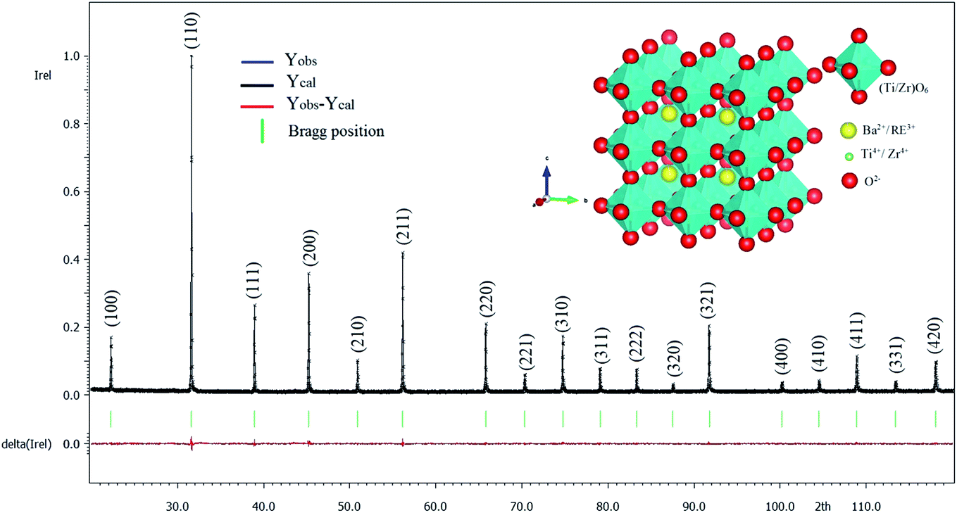 | ||
| Fig. 2 X-ray diffraction refinement for BLaZT powder, and crystal structure of BLaZT sample drawn with the help of “VESTA” software in Pmm space group. | ||
Fig. 2 shows the Rietveld refinement for the compound BLaZT to illustrate the quality of the refinement in the Pmm space group. All diffraction peaks (hkl) are listed, with their intensity and shape reproduced satisfactorily using the refined parameters. The fit between the experimental and calculated models is relatively good, the quality of the refinements is sufficient to discuss the proposed structural model and study the structural parameters in more detail.
The refined cell parameters of the compounds BZT, BSmZT and BLaZT are respectively 4.18061(11), 4.17226(11) and 4.17882(12). This result suggests that the unit cell volume decreases when rare earths are inserted into the A site. The reduction of the unit cell volume is on the basis of the difference in ionic radius between Ba2+ and RE3+. According to the Shannon's database,62 the effective ion radius for coordination 12 is 1.61 Å and (1.36 Å and 1.24 Å) for Ba2+ and (RE3+ = La3+ and Sm3+) ions, respectively. Consequently, the reduction in unit cell volume can be attributed to the substitution of RE3+ for Ba2+.
The crystal structure of the studied BLaZT compound designed with the help of “VESTA” software in Pmm space group is given in the inset of Fig. 2. It is obviously noticed that the cations Ti4+ and Zr4+ form with the oxygen anions regular (Ti/Zr)O6 octahedra, these are not distorted due to the higher symmetry of the cubic Pmm space group.9,63,64 The (Ti/Zr)O6 octahedra are connected in three dimensions by oxygen anions. In addition, Ba2+ and La3+ are surrounded by 12 oxygen anions, giving (Ba/La)O12 polyhedra.
The refined cell parameters and the reliability factors are given in Table S1.† The refined structural parameters (atomic positions, thermal agitation factors, and occupation rates) are presented in Table S2.† The selected bond distances and angles are summarized in Table S3.†
4.2 Density and microstructure of ceramic samples
The relative density (ρr) of the prepared ceramics was determined using the following equation61,65| ρr = ρm/ρt | (5) |
The relative density ρr is defined as the ratio between the measured density (ρm = m/v) and the theoretical density (ρt = ZM/V0Na), where m, v, M, V0 and Na are the mass of pellet, volume of pellet, molar mass, volume of unit cell and Avogadro's constant.
The densities of the prepared ceramics are shown in Table 1. The relative densities of the BZT, BLaZT, and BSmZT ceramics are 94.01%, 95.59%, and 95.74%, respectively, suggesting that all samples are well densified.
| Composition (x) | ρm (g cm−3) | ρt (g cm−3) | ρr (%) |
|---|---|---|---|
| BZT | 5.817 | 6.012 | 96.92 |
| BLaZT | 5.854 | 6.117 | 95.68 |
| BSmZT | 5.846 | 6.087 | 96.05 |
The microstructure of the BZT, BLaZT and BSmZT pellets sintered at 1450 °C for 6 h together and the results of grain size analysis are shown in Fig. 3. The SEM images presented in Fig. 3 show a homogeneous distribution of unequal size on the totality of the surfaces of all the ceramics. The absence of voids suggests that the samples are well densified, in agreement with the measured relative densities (see Table 1). The histograms of Fig. 3 indicate that the average grain sizes calculated using ImageJ software for BZT, BLaZT and BSmZT ceramics are respectively 1.19, 2.32 and 1.71 μm.
 | ||
| Fig. 3 SEM images of the surface of BZT, BLaZT and BSmZT ceramics and associated grain size distributions. | ||
4.3 Study of dielectric properties
Fig. 4a–c illustrates the variation of the relative permittivity for BZT, BLaZT and BSmZT ceramics as a function of frequency for different temperatures. It can be observed that the relative permittivity decreases progressively as the frequency increases from 10 Hz to 100 Hz and is approximately constant at frequencies above 100 Hz for BZT ceramic but for BLaZT and BSmZT ceramics the value of the relative permittivity becomes constant at frequencies above 1 kHz. It is well known that as the frequency increases, the relative permittivity decreases gradually, which is a common characteristic of dielectric materials. The high permittivity in the low frequency region is caused by the different types of polarization present in these materials, including dipolar, atomic, ionic, electronic, etc.66,67 For high frequencies, the relative permittivity decreases and reaches a plateau, this behavior suggests the presence of charged species (grain boundary effect, oxygen vacancies.) which are unable to follow the variation of the applied alternating electric field for high frequencies.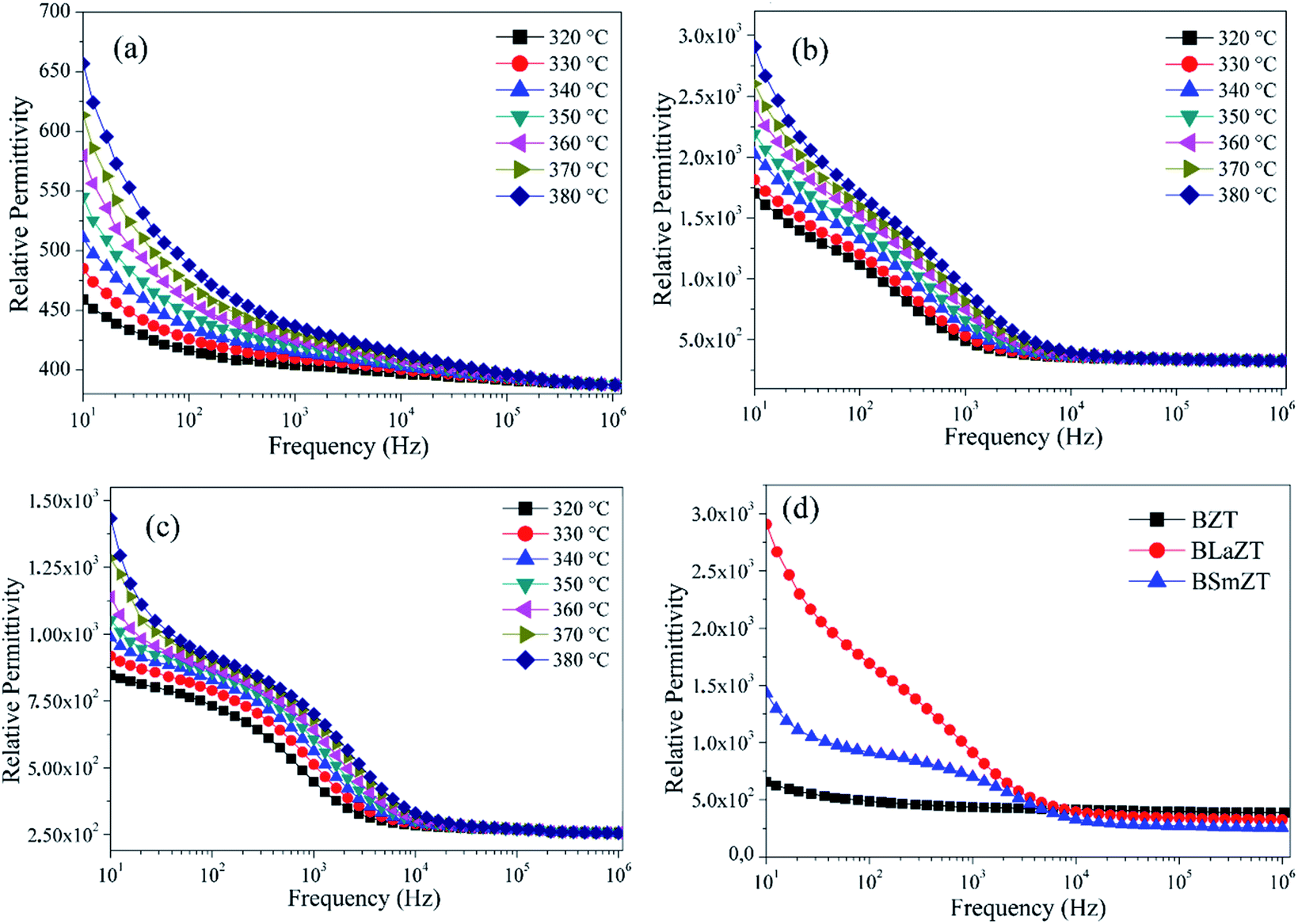 | ||
| Fig. 4 Relative permittivity at different temperatures for; (a) BZT, (b) BLaZT, (c) BSmZT and (d) comparison of relative permittivity for BZT, BLaZT and BSmZT ceramics at 380 °C. | ||
For BLaZT and BSmZT ceramics (Fig. 4b and c), it is obvious that the (ε′) spectra shows two relaxation processes in the low- and high-frequency domain at all temperatures. The shifting of relaxation peak corresponds to the relaxation process towards higher frequencies with increase in temperature evidenced a thermally activated dielectric relaxation.68 These two relaxations can be clearly visualized from (Fig. 14) modulus formalism (M′′ vs. frequency plots). It is suggested that the low frequency dielectric relaxation with high (ε′) values may be caused by extrinsic contribution such as space charge localization at the grain boundaries, electrode interface effect and some intrinsic effects such as voids/dislocations, defect complex or both may be involved in this process.69,70
Fig. 4d shows the relative permittivity of BZT, BLaZT and BSmZT ceramics at 380 °C, their values being 436.75, 913.81, and 701.21 at 1 kHz respectively. We notice that the relative permittivity of rare earth doped BZT ceramics are higher than that of BZT, this is due to the insertion of rare earths in the A site of the perovskite structure.
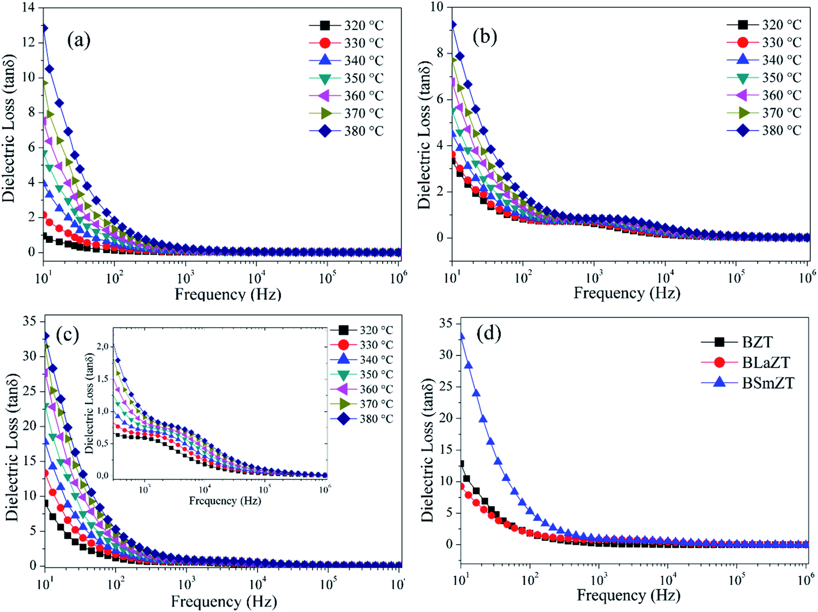
Fig. 5a–c shows the variation of the dielectric loss (tanδ) with frequency at different temperatures, it presents the same behavior as that of the relative permittivity (ε′), i.e. it decreases with the increase of the frequency. This decrease in dielectric loss (tanδ) with increasing frequency is attributed to the phenomenon of dipolar relaxation. The space charges are not able to follow the high frequency of the applied electric field and go through relaxation.71 The increase in dielectric loss values as a function of temperature may be due to thermally activated charge carriers. However, the origin of this behavior must be identified by complex impedance spectroscopy, in terms of analysis of the real and imaginary part of the complex impedance, analysis of the AC conductivity and study of the dielectric modulus.
 | ||
| Fig. 5 Dielectric losses at different temperatures for; (a) BZT, (b) BLaZT, (c) BSmZT and (d) comparison of dielectric losses (tanδ) for BZT, BLaZT and BSmZT ceramics at 380 °C. | ||
Fig. 5d illustrates the dielectric loss tan(δ) values for the BZT, BLaZT and BSmZT ceramics at 380 °C as a function of frequency. The values of tan(δ) at 1 kHz are 0.2466, 0.8432, and 0.9771, respectively.
4.4 Complex impedance analysis (CIA)
Fig. 6 shows Nyquist plots for BZT, BLaZT and BSmZT ceramics at different temperatures, and a comparison of the diagrams at 380 °C. As predicted, the diagrams appear more or less as semicircles, with their center above the real axis. With increasing temperatures, these semicircles become more complete in the measured frequency range (10 Hz to 1 MHz). Since the intersection of the semicircle on the real axis (Z′) directly corresponds to the global circuit resistance “R”, this value has a strong effect on the magnitude of real and imaginary part of the impedance.72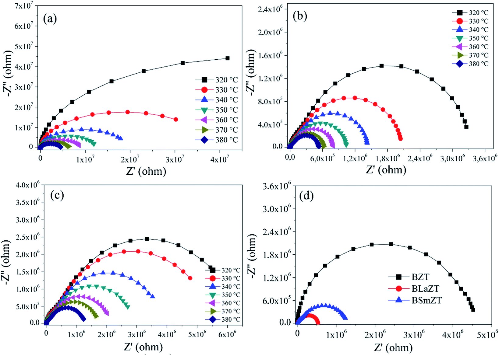 | ||
| Fig. 6 Complex impedance diagram at different temperatures for; (a) BZT, (b) BLaZT, (c) BSmZT and (d) comparison of diagrams for BZT, BLaZT and BSmZT ceramics at 380 °C. | ||
For BZT ceramics the Nyquist diagram (Fig. 6a) shows a single semicircular arc up to 380 °C representing a grain contribution, but for BLaZT and BSmZT ceramics (Fig. 6b and c) we observe the appearance of two overlapping semicircular arcs suggesting the contribution of grains and grain boundaries. Obviously, the diagrams (Fig. 6d) show that the radius of the semicircle decreases, i.e. the resistance decreases with the insertion of rare earths in the perovskite A.
However, fitting of the experimental data with the suitable equivalent electrical circuit, indicated that the data are in good agreement with the series connection of two cells, associated with grains and grain boundaries effects respectively for BLaZT and BSmZT ceramics. For BZT ceramics, the equivalent circuit used to describe the electrical properties is composed of a single branch, which represent the electrical properties of grains. In addition, the MT-Lab software can be used to adjust the parameters of each element in the equivalent circuit shown in Fig. 7.
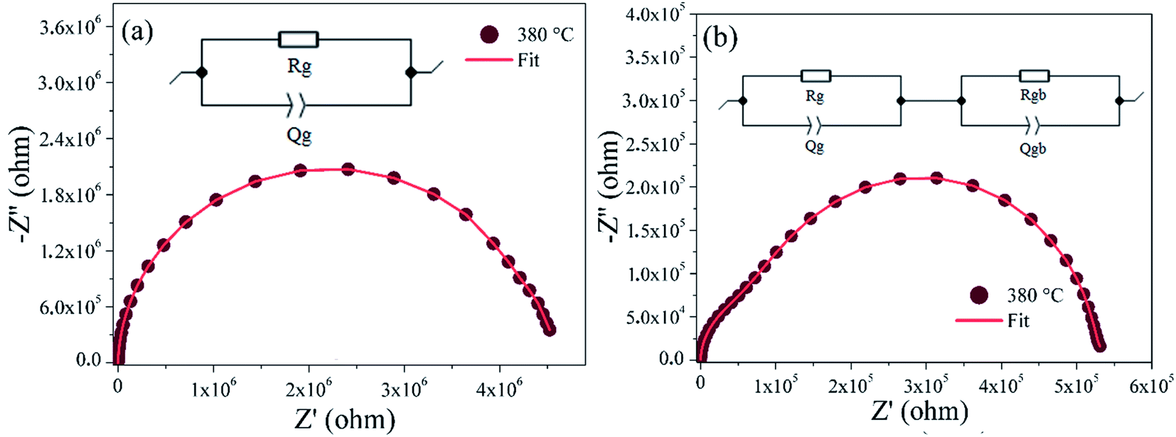 | ||
| Fig. 7 Adjusted Nyquist diagram for: (a) BZT, and (b) BLaZT at 380 °C. The solid red lines show the data adjusted with the MT-Lab software. | ||
We used a series combination of two parallel circuits to characterize respectively the effect of grains and grain boundaries for the rare earth-doped BZT ceramics. In the first parallel circuit corresponding to the grain contribution, Rg and Qg correspond to the grain resistance and the constant phase element. In the second parallel circuit, Rgb and CPE were used as grain boundary resistance and constant phase element.
A constant phase element (CPE) is added into the circuit, because of the non-ideal capacitive behavior. The constant phase element (Q) is estimated by the following relationship:58,73–75
| C = (R1−αQ)1/α | (6) |
For an ideal resistor and an ideal capacitor, the “α” values are respectively zero and one.76 A good agreement between the experimental data and the calculated values gives us confidence in the proposed equivalent circuits. The various adjusted parameters are presented in Table S4.† The values of Rg and Rgb decrease when rare earths (RE = La, Sm) are introduced into the A-site of the perovskite structure. The decrease in grain resistance with the substitution of rare earths in the BZT lattice may be due to the increase in grain size in the (Ba1−xRE2x/3)(Zr0.9Ti0.1)O3 ceramics (see Fig. 3). In another way, the values of Rg and Rgb decrease with the increasing temperatures for all ceramics, showing the occurrence of a thermally activated conduction mechanisms in the grains and at the grain boundaries.
4.5 Conductivity study
In general, the weakly bound charge carriers migrate in dielectric compounds, when the electric field is applied, which is called electrical conduction. The conduction process is usually dominated by anions/cations or holes/electrons or oxygen vacancies. Usually, in perovskites, the electrical polarization is considered to be the result of vacancies (oxygen), polarons and electrons liberated by the ionization of vacancies (oxygen).77Conductivity values were calculated from the dielectric data using the relationship:
|
σAC = ωε0εrtanδ
| (7) |
The AC conductivity (Fig. 8a–c) increases with increasing frequency for all temperatures. The AC conductivity at each measured temperature presents two separate regions. For low frequencies, a first region is observed where the conductivity does not change with frequency. For the second region, the conductivity increases with increasing frequency. This type of AC conductivity can be explained by Jonscher's power law.78,79
| σAC = σDC + Aωs | (8) |
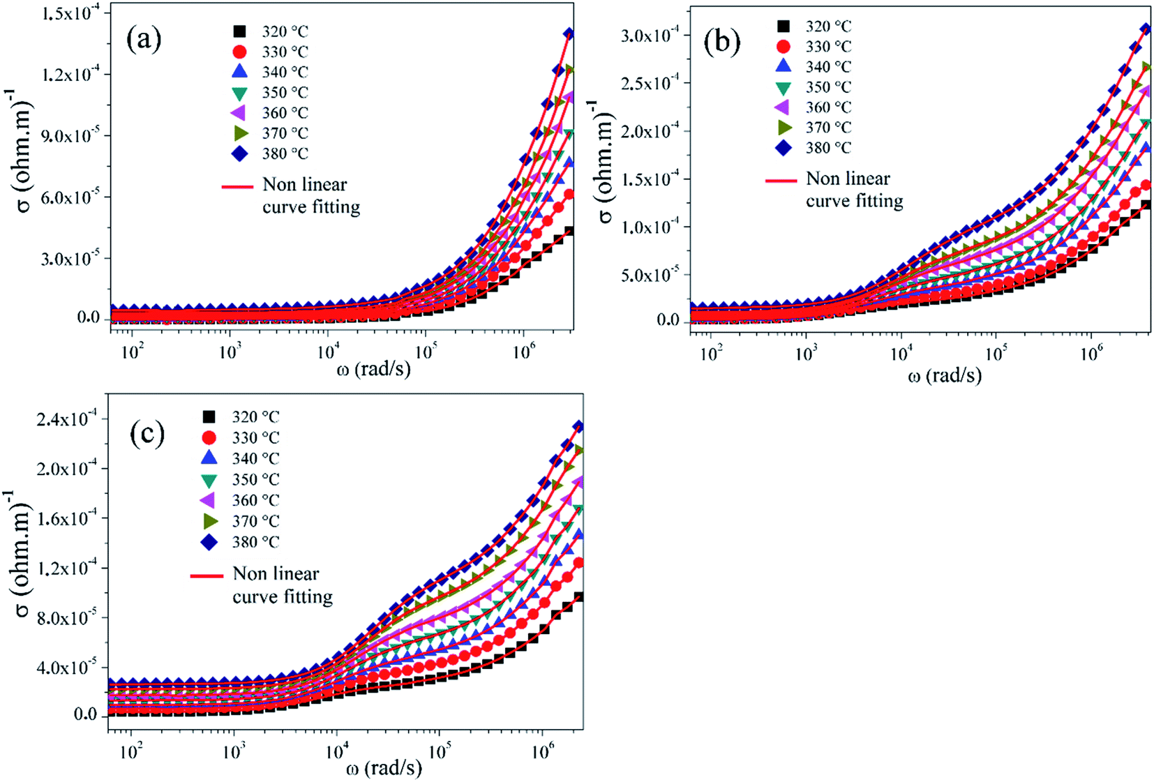 | ||
| Fig. 8 AC conductivity as a function of frequency at different temperatures for; (a) BZT, (b) BLaZT, and (c) BSmZT. | ||
Funke has explained80 the physical meaning of the numerical values of the “s” parameter. s ≤ 1 means that the hopping motion involves a translational motion with a sudden hopping, whereas s > 1, means that the motion involves localized hopping without the species leaving the neighborhood.
In particular, in the situation of structurally disordered materials, if an ion hops to a neighboring vacant site, there is a high probability that the ion will return to its previous position (an unsuccessful hop). However, if the neighborhood becomes relaxed relative with respect to the ion's position, the ion will remain in the new site (successful hop). The conductivity in the low frequency region is associated with successful hops. In the low frequency range (plateau region), the conductivity (σDC), is entirely determined by successful hops. At higher frequencies, above the plateau, many hops are unsuccessful, and as the frequency increases, the number of these unsuccessful hops increases. The change in the ratio of successful to unsuccessful hops results in dispersive conductivity.81
By fitting eqn (8) to the experimental data, it has been observed that the experimental results do not follow the Jonscher power law for BLaZT and BSmZT ceramics. This disagreement may be attributed to the presence of two different types of charge carriers hoping near the grains and grain boundaries. Subsequently, the modified Jonscher power law (eqn (9)) was used to correctly explain the AC conductivity spectra of BLaZT and BSmZT ceramics (Fig. 9b and c).
| σAC = σDC + A1ωs1 + A2ωs2 | (9) |
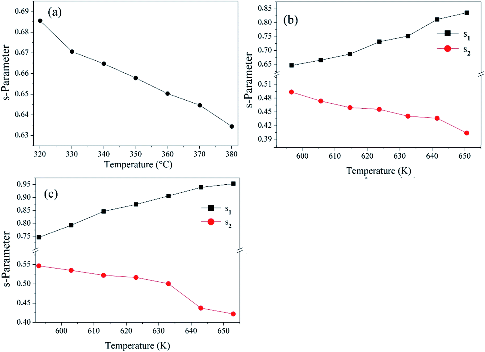 | ||
| Fig. 9 Variation of the “s” parameter with temperature for; (a) BZT, (b) BLaZT, and (c) BSmZT. | ||
The term A1ωs1 represents the dispersive region due to the hopping of charge carriers in the grain, while A2ωs2 characterizes the hopping of charge carriers in the grain boundaries.
The fit parameters σDC, A1, s1, A2, and s2 calculated from the nonlinear fit are presented in Table S5.† It is evident that σDC increases with temperature for all ceramics in the selected temperature range which suggests the semiconducting behavior of our compounds. This increase can be attributed to the reduction of the encountered barriers for the transport of charge carriers by the thermal energy effect. On the other hand, it shows that if rare earths (RE = La, Sm) are inserted in the A site of the BZT structure, the conductivity increases. This improvement of the electrical conductivity can be associated to the substitution of Ba by (RE = La, Sm), this heterogeneous substitution leads to the creation of barium vacancies  .
.
The conduction mechanism in BZT, BLaZT and BSmZT compounds was determined by analyzing the temperature dependence of the “s” parameter. From Fig. 9a–c, the behavior of “s” changes with the insertion of rare earths into the A site of the BZT structure and also with increasing temperature. A correlation between the conduction mechanism and s(T) behavior could suggest an appropriate model of this conduction mechanism.82 Based on two different processes, the classical hopping over a potential barrier and the quantum-mechanical tunneling, or a combination of both, it has been supposed that the responsible charge carriers could be electrons or ions.83 These different models have been determined based on the behavior of the parameter “s”.
In fact, when the exponent “s” decreases with increasing temperature, the correlated barrier hopping (CBH) is the appropriate model.84 As the exponent “s” is practically constant (equal to 0.8) and independent of temperature or increases slightly with temperature, the most appropriate model is the Quantum Mechanical Tunneling (QMT).85 When the exponent depends on both temperature and frequency and decreases with increasing temperature to a minimum value, after increases as temperature increases, the model is Overlapping Large-Polaron Tunneling (OLPT).86 Finally, if the exponent “s” increases with the increase in temperature, the corresponding model is Small Polaron Tunneling without overlap (NSPT).82
To identify the appropriate mechanism for conductivity, the variation of the exponent “s” with temperature was represented in Fig. 9.
For BZT compound (Fig. 9a), “s” decreases as the temperature increases. This behavior is in good agreement with the Correlated Barrier Hopping (CBH) model. Therefore, based on this model, AC conductivity is a result of the hopping of charge carriers between two sites over the potential barrier separating them, because of thermal activation.87
The BLaZT and BSmZT samples (Fig. 9b and c), present two different behaviors for the parameter “s”:
• “s1” increases with the rise in temperature. This evolution can therefore be explained by the Small Polaron Tunneling without overlap (NSPT).
• “s2” decreases with increasing temperature. This evolution can therefore be explained by the Correlated Barrier Hopping (CBH).
Fig. 10 presents the variation of ln(σDC) with the inverse of the temperature (103/T), which leads to the value of the activation energy for the electrical conduction of BZT, BLaZT and BSmZT ceramics, calculated by Arrhenius' law.
|
σDC = σ0exp(−Ea/kBT)
| (10) |
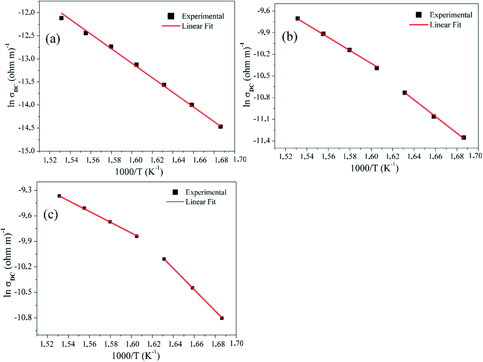 | ||
| Fig. 10 Conductivity ln(σDC) as a function of 1000/T for; (a) BZT, (b) BLaZT, and (c) BSmZT ceramics. | ||
| Compound | Ea/eV (grain) | Ea/eV (grain boundary) |
|---|---|---|
| BZT | 1.161 ± 0.023 | — |
| BLaZT | 1.057 ± 0.029 | 0.766 ± 0.021 |
| BSmZT | 1.064 ± 0.024 | 0.836 ± 0.022 |
For BZT ceramics (see Fig. 10a), we have found a single activation energy which is associated with grain contribution, but for BLaZT and BSmZT ceramics (Fig. 10b and c), two activation energies have been obtained, corresponding to the grains and grain boundaries, respectively. It should be noted that the activation energy of the grains is higher than that of the grain boundaries. This signifies that the grains have a higher resistance than the grain boundaries, as previously obtained from Nyquist plots (see Table S4†).
In ferroelectric oxides, the thermal activation energy is strongly related to the concentration of oxygen vacancies (OVs). A stoichiometric perovskite ABO3 has an activation energy Ea = 2 eV, while the value of Ea is 1 eV for ABO2.95 and 0.5 eV for ABO2.90.88,89 From Table 2, the values of the activation energy Ea of the grain and grain boundary are smaller than 2 eV, which indicates that oxygen vacancies are responsible for the conduction mechanism in BZT, BLaZT and BSmZT ceramics. Furthermore, it is known that the most mobile ionic species in oxide materials (perovskite, tungsten bronze lattice) are single and double ionized oxygen vacancies. It has often been mentioned that the activation energy of single ionized oxygen vacancies is about (0.3–0.5 eV) and about (0.6–1.2 eV) for double ionized oxygen vacancies.59,65,90
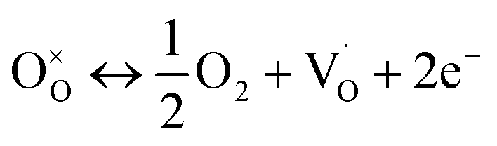
Oxygen vacancies are considered as one of the mobile charge carriers and, mainly in titanates, the ionization of oxygen vacancies creates conduction electrons, a process that is described by the Kröger–Vink notation.91
 | (11) |
Oxygen vacancies (OVs) can easily be created in oxide materials by the loss of oxygen from the crystal lattice during heating at elevated temperatures (typically >1300 °C).92
The single and double ionized oxygen vacancies will create the conducting electrons, written as
 | (12a) |
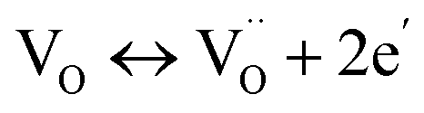 | (12b) |
Returning to the chemical composition of the studied perovskite ceramics, we point out that the substitution of Ba2+ by La3+ or Sm3+ could induce the creation of some defects, this heterovalent substitution can be expressed by the Kröger–Vink notation;
 | (13) |
 is necessary for charge neutrality in the perovskite structure. Consequently, the second activation energy that was not detected in BZT ceramics is due to the creation of Barium vacancies
  in the BLaZT and BSmZT structure. In addition, our Ea results for grains and grain boundaries (see Table 2) are very close to the activation energy of the ion conductivity induced by doubly ionized oxygen vacancies (OVs) in perovskite and tungsten bronze type ferroelectric oxides reported by many authors.57,59,65,71,73,93,94 Therefore, we can realistically conclude that the conducting species in BZT, BLaZT and BSmZT ceramics are double ionized oxygen vacancies (OVs).
| Compound | Ea/eV (grain) | Ea/eV (grain boundary) |
|---|---|---|
| BZT | 1.166 ± 0.021 | — |
| BLaZT | 0.906 ± 0.024 | 0.831 ± 0.022 |
| BSmZT | 0.968 ± 0.027 | 0.887 ± 0.023 |
4.6 Complex electrical modulus
The complex analysis of the dielectric modulus is a practical tool for studying electrical transport phenomena in ceramics and for distinguishing the microscopic processes responsible for dielectric relaxation.95 The complex dielectric modulus, M*, is given by the inverse of the complex dielectric constant. The modulus data were calculated by using eqn (4).The variation of the imaginary part of the modulus M′′ as a function of frequency is shown in Fig. 11a–c. The variation of M′′ as a function of frequency is characterized by a single peak for the BZT compound (Fig. 11a) and two relaxation peaks for the rare-earth-doped BZT compounds (Fig. 11b and c), one asymmetric peak at low frequency and the other at high frequency which is fundamentally due to the relaxation process of grains and grain boundaries, respectively. We can observe that the position of the relaxation peaks moves to higher frequencies when the temperature increases. The low frequency side of the imaginary part of the modulus defines the range in which the charge carriers are mobile over long distances.
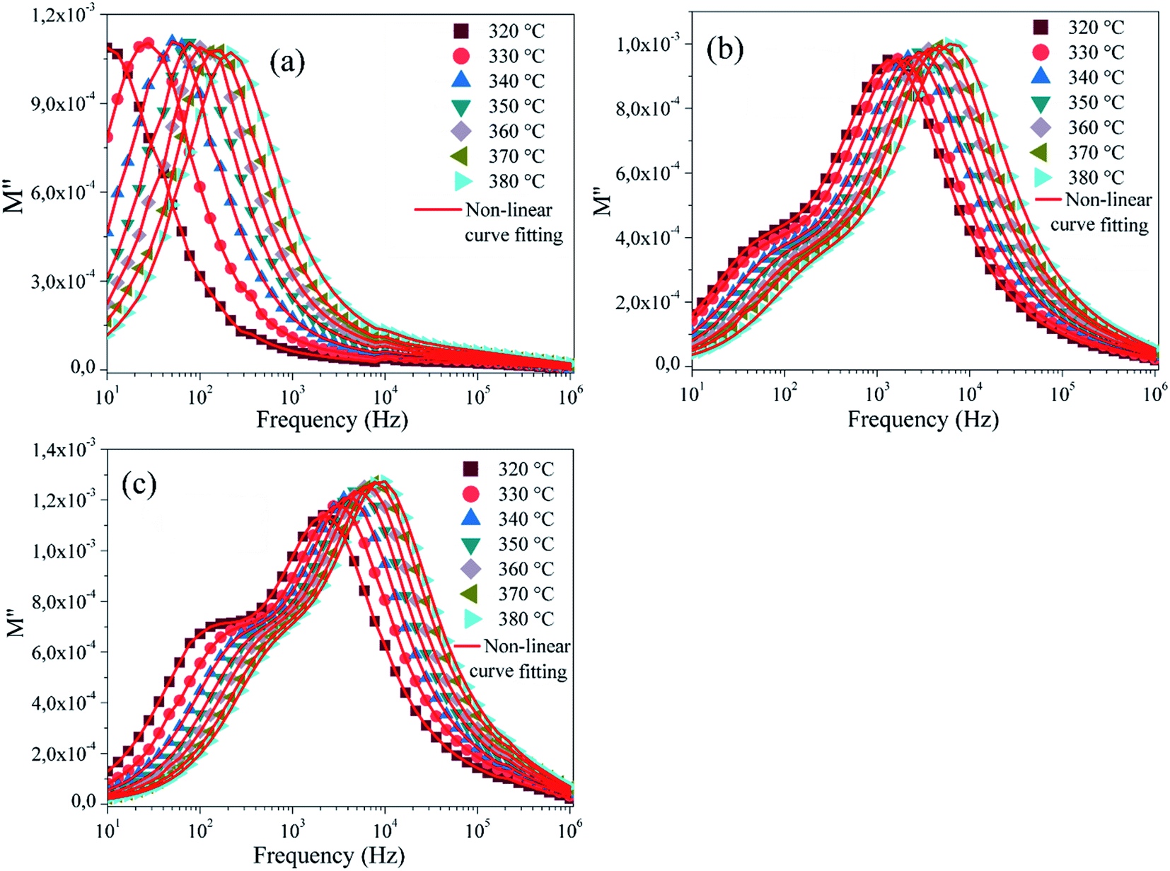 | ||
| Fig. 11 Imaginary part of the modulus M′′ as a function of frequency at different temperatures for; (a) BZT, (b) BLaZT, (c) BSmZT and (d) The plot of β-parameter versus temperature. | ||
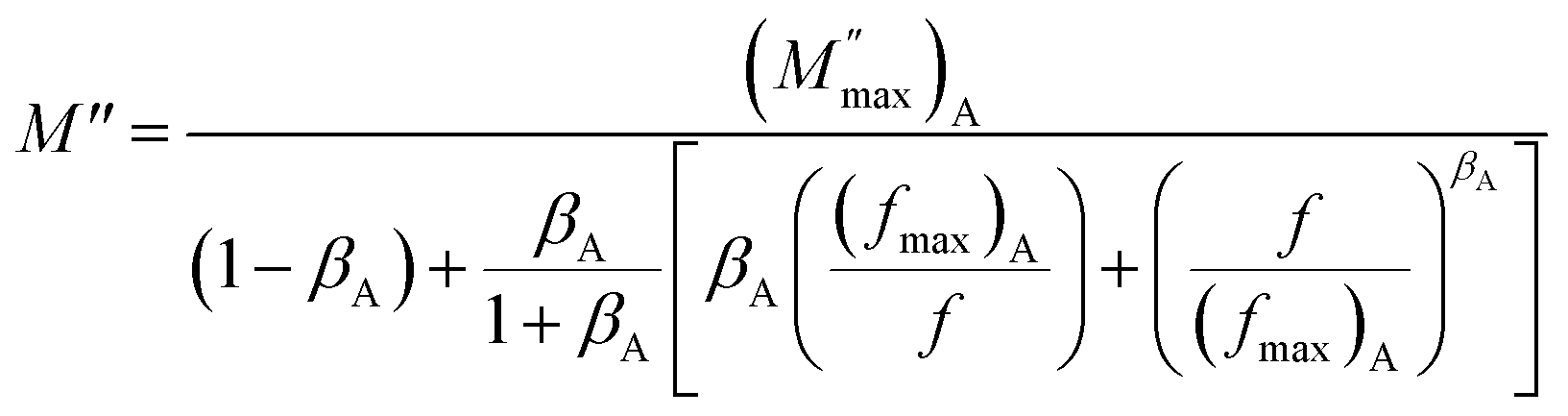
In order to identify some characteristic parameters of the charge carriers such as their activation energy and relaxation frequency, numerical fitting of modulus spectra is interesting. Bergman has suggested a function that describes the variation of the imaginary part of the modulus M′′ in the frequency domain.96
 | (14) |
 | (15) |
 and
and  are the peak values of M′′ for relaxation A and relaxation B, respectively, and (fmax)A and (fmax)B are the corresponding relaxation frequencies. For an ideal Debye type relaxation, β = 1 and for non-Debye type relaxation, (0 < β < 1).
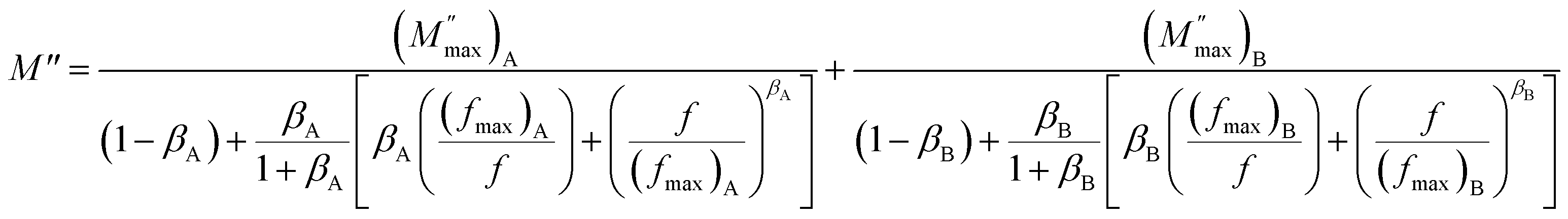
By fitting eqn (14) to the experimental data, it was observed that the experimental results do not follow the Kohlrausch–Williams–Watts function proposed by Bergman for BLaZT and BSmZT ceramics. This disagreement can be attributed to the presence of two different types of relaxations. Subsequently, the modified Kohlrausch–Williams–Watts (KWW) function (eqn (15)) was used to correctly explain the spectra of the imaginary part of the M′′ modulus of BLaZT and BSmZT ceramics (Fig. 11b and c).
The red lines in Fig. 11 represent the fitting of testing data based on eqn (14) and (15). The results in Fig. 12 indicate that the value of (β) increases with increasing temperature, and for all three ceramics the β values are between 0 and 1 (0 < β < 1). These results confirm that the relaxation process is non-Debye type in BZT, BLaZT and BSmZT ceramics.
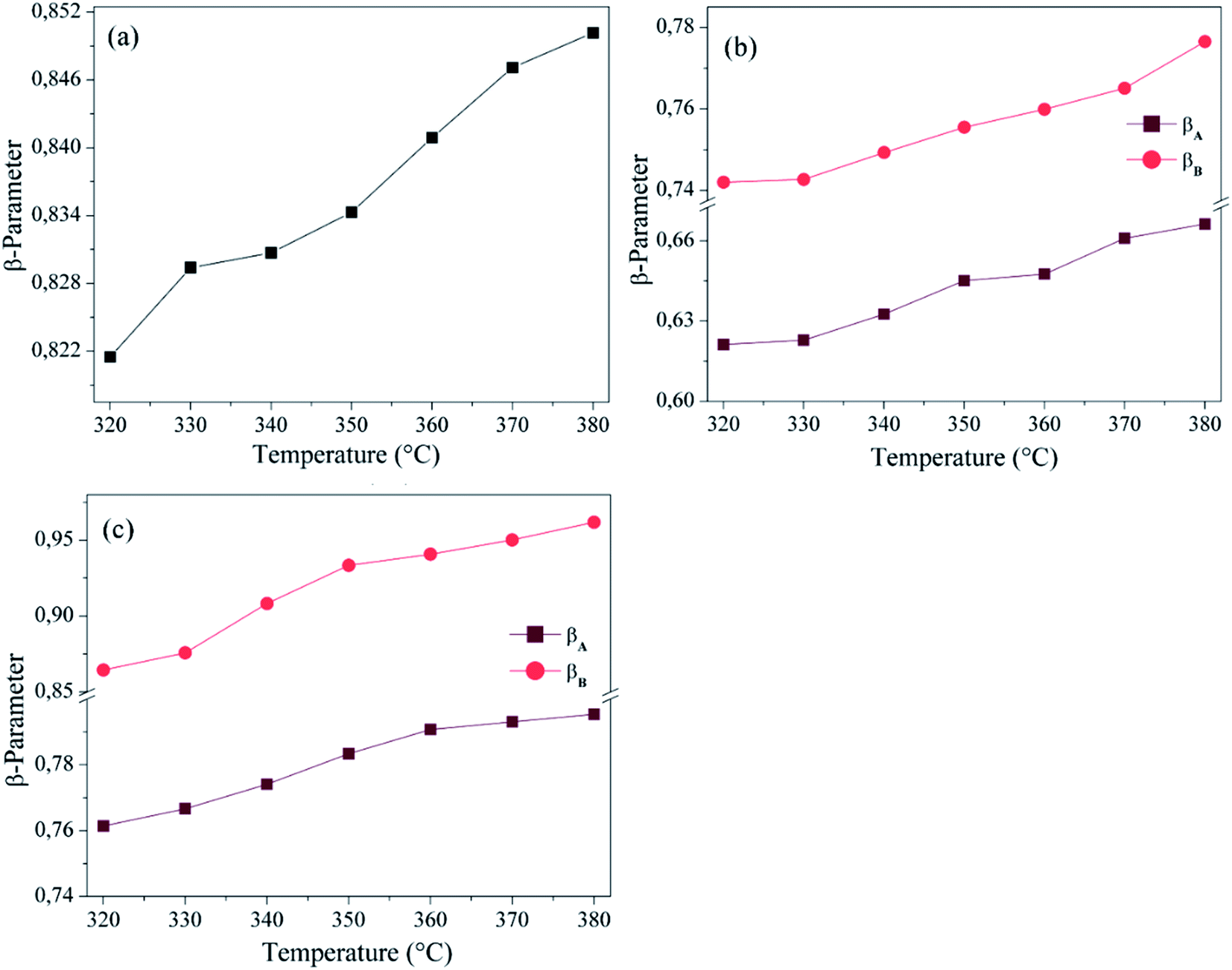 | ||
| Fig. 12 The plot of β-parameter versus temperature; (a) BZT, (b) BLaZT, (c) BSmZT. | ||
To confirm the possible contribution of grain and grain boundary, the  peak of the imaginary part of module was decomposed by Gaussian–Lorentzian curve fit at 380 °C (Fig. 13a and b). It is an effective strategy for identifying the dielectric responses from grain, grain boundary and electrode effect although with very small differences.73,97
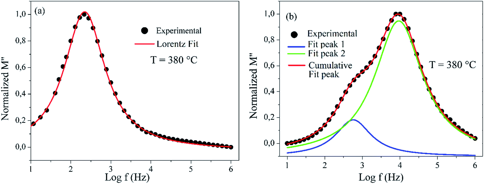 | ||
| Fig. 13 Deconvolution of M′′ spectra of; (a) BZT and (b) BLaZT ceramics distinguishing the overlapped peaks. | ||
From Fig. 13, for BZT ceramics we can see that we have only the grain contribution but for BLaZT and BSmZT ceramics, the  peak is the result of two overlapping peaks. The peak in blue represents the grain contribution, while the peak in green represents the grain boundary contribution. These results were confirmed by fitting the Nyquist plots with circuits corresponding to the grain contribution only for BZT ceramics and grain and grain boundary contribution in the case of BLaZT and BSmZT ceramics (see Fig. 7).
The variation of the relaxation time (τ) as a function of 103/T for BZT, BLaZT and BSmZTceramics in the high-temperature region is presented in Fig. 14 (calculated from the imaginary part of modulus pattern). These plots follow the Arrhenius relation: τ = τ0exp(−Ea/kBT), where the symbols have their usual meanings and the process thermally activated. The values of the activation energy found from linear fit are presented in the Table 3.
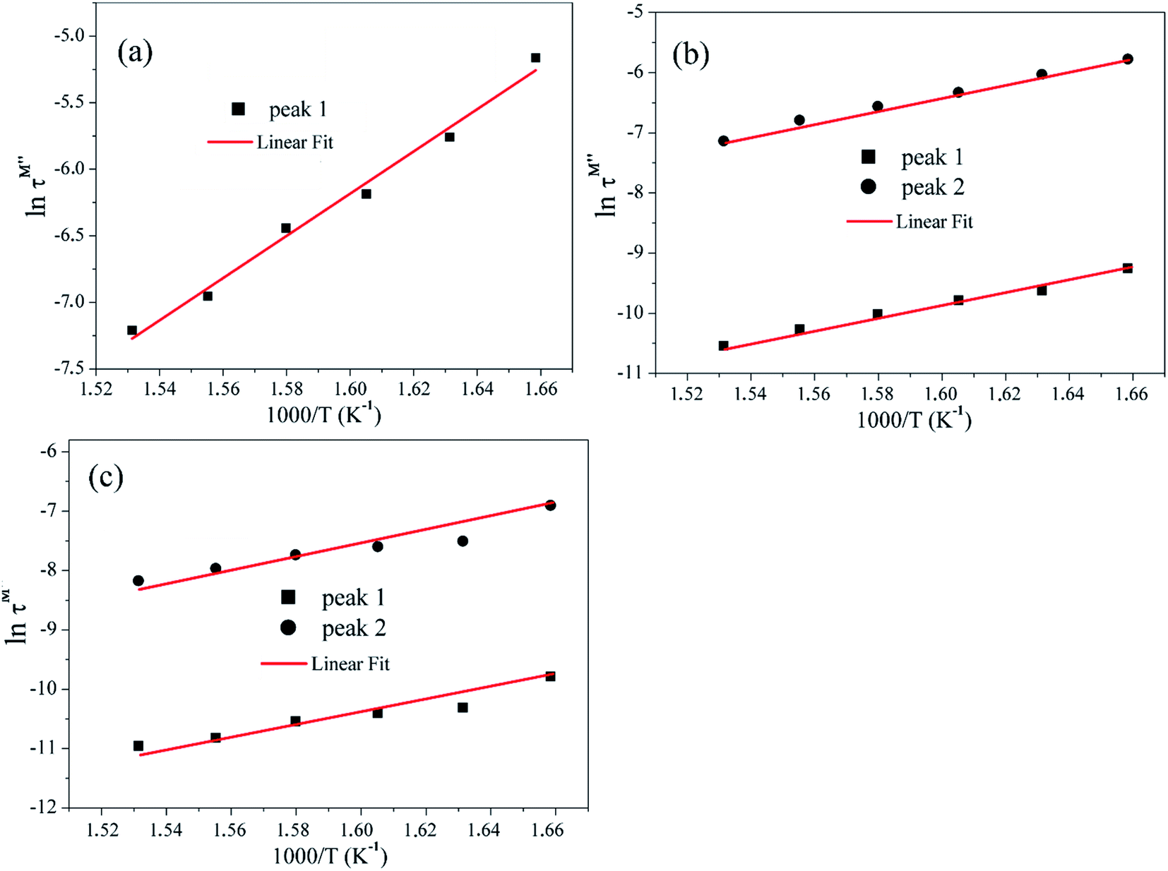 | ||
| Fig. 14 Variation of ln(τ) with 103/T for; (a) BZT, (b) BLaZT and (c) BSmZT ceramics. | ||
The spectrum of the complex modulus of M′′ versus M′ at various temperatures for the BZT, BLaZT and BSmZT ceramics is illustrated in Fig. 15. The Fig. 15a shows only one semicircular arc behavior for BZT ceramics which means that we have only the contribution of the grains. For the BLaZT and BSmZT ceramics (Fig. 15b and c), the data reveals two well resolved semicircles: the first semicircle at low frequency represents the capacitive effect of the grain boundaries and the second at high frequency represents the capacitive effect of the grains at all measured temperatures (320–380 °C). This behavior has been visualized by the Nyquist plot (Fig. 7) and from the variation of the imaginary part of the modulus as a function of frequency (Fig. 11).
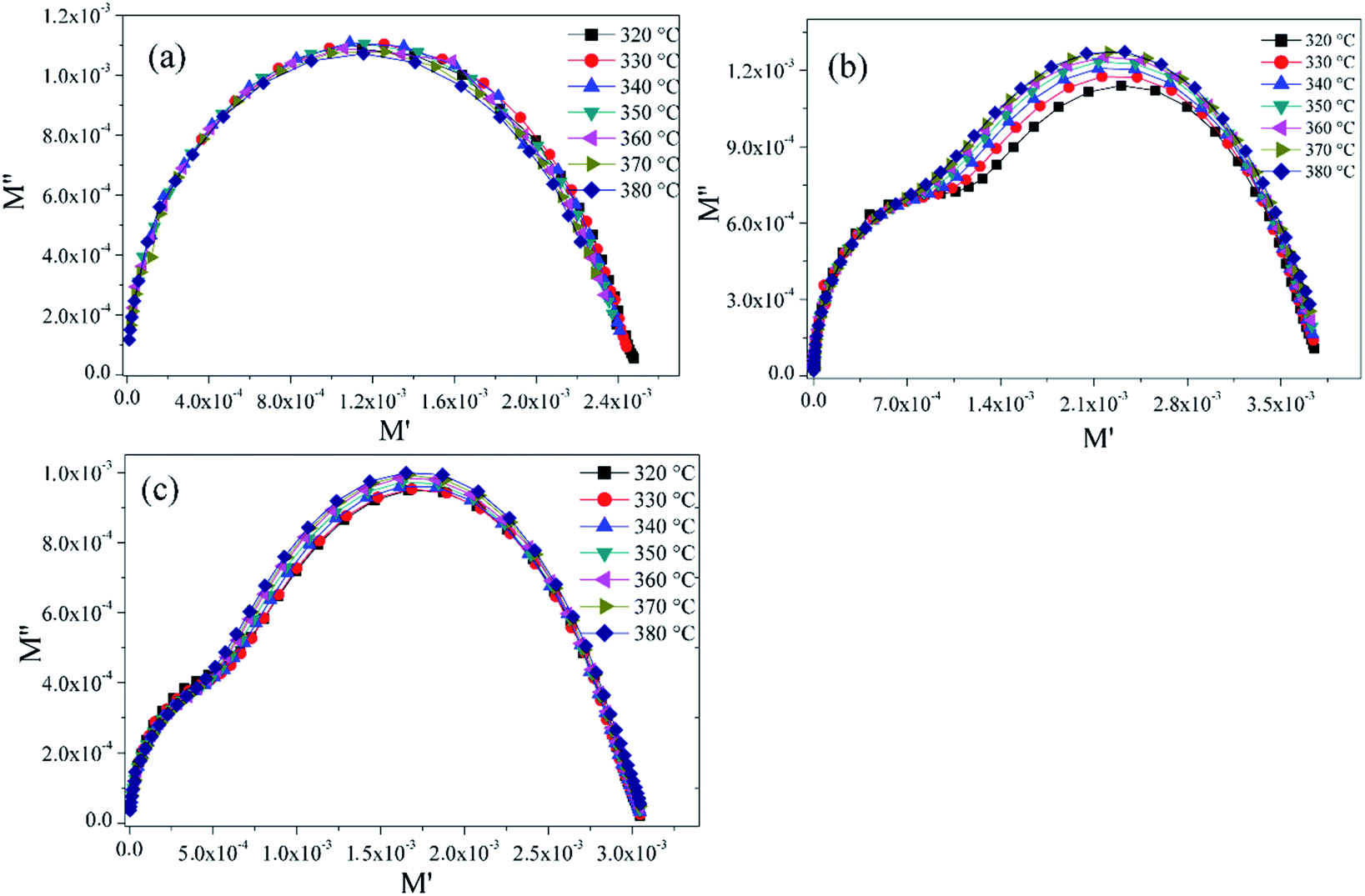 | ||
| Fig. 15 Complex modulus spectrum at different temperatures for; (a) BZT, (b) BLaZT, and (c) BSmZT. | ||
5. Conclusion
Ba(Zr0.9Ti0.1)O3 and ((Ba0.9RE0.067)(Zr0.9Ti0.1)O3, RE3+ = La3+, Sm3+) are prepared at high calcination temperature (1350 °C for 6 hours) by a solid state reaction method. Analysis of the XRD data by the Rietveld method showed a perovskite structure with the Pmm space group for all samples and confirmed that the cubic crystal structure is not modified by rare earths doping in the BZT structure. The SEM images showed a homogeneous microstructure consisting of unequal sized grains, high densification, and low porosity. The average grain size was in the range of 1.19–2.32 μm. The Cole–Cole diagrams of −Z′′ vs. Z′ and M′′ vs. M′ show that the electrical response of BZT ceramics doped with rare earths (Ba0.9RE0.067)(Zr0.9Ti0.1)O3, is due to grain and grain boundary effects and for Ba(Zr0.9Ti0.1)O3 ceramics, it was found that the grains only contributed to the conduction process. The conduction process for the Ba(Zr0.9Ti0.1)O3 sample is dominated by the Correlated Barrier Hopping (CBH) model, but for (Ba0.9RE0.067)(Zr0.9Ti0.1)O3 compounds the conduction is dominated by the Correlated Barrier Hopping (CBH) model at the grains and by the Small Polaron Tunneling without overlap (NSPT) model at the grain boundaries. The activation energies obtained from DC conductivity are comparable to these of modulus spectra, indicating that the conduction process and relaxation phenomena are associated to the same origin.
Conflicts of interest
There are no conflicts to declare.Acknowledgements
We are very grateful to “Centre Européen de la Céramique Limoges” for their help and support in the process of samples testing in this work. We thank greatly the anonymous reviewers for their careful review and valuable suggestions on the manuscript. Department of Chemistry – Multidisciplinary Faculty (FPN), is acknowledged for practical assistance with the recording of the spectral analysis.References
- A. Bokov and Z.-G. Ye, J. Mater. Sci., 2006, 41, 31–52 CrossRef CAS.
- X. Hao, J. Adv. Dielectr., 2013, 3, 1330001 CrossRef.
- A. Petraru, J. Schubert, M. Schmid and C. Buchal, Appl. Phys. Lett., 2002, 81, 1375–1377 CrossRef CAS.
- Y. Slimani, A. Selmi, E. Hannachi, M. Almessiere, M. Mumtaz, A. Baykal and I. Ercan, J. Mater. Sci.: Mater. Electron., 2019, 30, 13509–13518 CrossRef CAS.
- Y. Slimani, A. Selmi, E. Hannachi, M. Almessiere, A. Baykal and I. Ercan, J. Mater. Sci.: Mater. Electron., 2019, 30, 9520–9530 CrossRef CAS.
- B. Steinfeld, J. Scott, G. Vilander, L. Marx, M. Quirk, J. Lindberg and K. Koerner, J. Behav. Health Serv. Res., 2015, 42, 504–518 CrossRef PubMed.
- Y. Slimani, M. Almessiere, S. E. Shirsath, E. Hannachi, G. Yasin, A. Baykal, B. Ozcelik and I. Ercan, J. Magn. Magn. Mater., 2020, 510, 166933 CrossRef CAS.
- B. Luo, X. Wang, E. Tian, H. Song, G. Li and L. Li, J. Alloys Compd., 2017, 708, 187–193 CrossRef CAS.
- H. Trabelsi, M. Bejar, E. Dhahri, M. Valente and M. Graça, Phys. E, 2019, 108, 317–325 CrossRef CAS.
- D. Karoblis, A. Zarkov, K. Mazeika, D. Baltrunas, G. Niaura, A. Beganskiene and A. Kareiva, Ceram. Int., 2020, 46, 16459–16464 CrossRef CAS.
- Y.-H. Dong, H. Xian, J.-L. Lv, C. Liu, L. Guo, M. Meng, Y.-S. Tan, N. Tsubaki and X.-G. Li, Mater. Chem. Phys., 2014, 143, 578–586 CrossRef CAS.
- K. Tan, H. Rahman and H. Taib, Mater. Chem. Phys., 2020, 254, 123433 CrossRef CAS.
- V. Bhide, M. Hegde and K. Deshmukh, J. Am. Ceram. Soc., 1968, 51, 565–568 CrossRef CAS.
- S. Gupta, C. Harendranath and A. Kulkarni, Ceram. Int., 1997, 23, 191–196 CrossRef CAS.
- J. Yoo, Y. Lee, K. Yoon, S. Hwang, S. Suh, J. Kim and C. Yoo, Jpn. J. Appl. Phys., 2001, 40, 3256 CrossRef CAS.
- S. Smail, M. Benyoussef, K. Taïbi, N. Bensemma, B. Manoun, M. El Marssi and A. Lahmar, Mater. Chem. Phys., 2020, 252, 123462 CrossRef CAS.
- L. Liu, S. Zheng, Y. Huang, D. Shi, S. Wu, L. Fang, C. Hu and B. Elouadi, J. Phys. D: Appl. Phys., 2012, 45, 295403 CrossRef.
- S. Zheng, D. Shi, L. Liu, G. Li, Q. Wang, L. Fang and B. Elouadi, J. Mater. Sci.: Mater. Electron., 2014, 25, 4058–4065 CrossRef CAS.
- Q.-J. Liu, N.-C. Zhang, F.-S. Liu, H.-Y. Wang and Z.-T. Liu, Opt. Mater., 2013, 35, 2629–2637 CrossRef CAS.
- T. Maiti, R. Guo and A. Bhalla, Appl. Phys. Lett., 2006, 89, 122909 CrossRef.
- Z. Yu, C. Ang, R. Guo and A. Bhalla, Appl. Phys. Lett., 2002, 81, 1285–1287 CrossRef CAS.
- X. Tang, K.-H. Chew and H. Chan, Acta Mater., 2004, 52, 5177–5183 CrossRef CAS.
- B. Asbani, J.-L. Dellis, A. Lahmar, M. Courty, M. Amjoud, Y. Gagou, K. Djellab, D. Mezzane, Z. Kutnjak and M. El Marssi, Appl. Phys. Lett., 2015, 106, 042902 CrossRef.
- H. Kaddoussi, Y. Gagou, A. Lahmar, J. Belhadi, B. Allouche, J.-L. Dellis, M. Courty, H. Khemakhem and M. El Marssi, Solid State Commun., 2015, 201, 64–67 CrossRef CAS.
- H. Kaddoussi, A. Lahmar, Y. Gagou, J.-L. Dellis, H. Khemakhem and M. El Marssi, Ceram. Int., 2015, 41, 15103–15110 CrossRef CAS.
- Y. Bai, X. Han and L. Qiao, Appl. Phys. Lett., 2013, 102, 252904 CrossRef.
- H. Kaddoussi, A. Lahmar, Y. Gagou, B. Manoun, J. Chotard, J.-L. Dellis, Z. Kutnjak, H. Khemakhem, B. Elouadi and M. El Marssi, J. Alloys Compd., 2017, 713, 164–179 CrossRef CAS.
- H. Kaddoussi, Y. Gagou, A. Lahmar, B. Allouche, J. Dellis, M. Courty, H. Khemakhem and M. El Marssi, J. Mater. Sci., 2016, 51, 3454–3462 CrossRef CAS.
- M. Benyoussef, J. Belhadi, A. Lahmar and M. El Marssi, Mater. Lett., 2019, 234, 279–282 CrossRef CAS.
- H. Cheng, J. Ouyang, Y.-X. Zhang, D. Ascienzo, Y. Li, Y.-Y. Zhao and Y. Ren, Nat. Commun., 2017, 8, 1–7 CrossRef.
- A. A. Instan, S. P. Pavunny, M. K. Bhattarai and R. S. Katiyar, Appl. Phys. Lett., 2017, 111, 142903 CrossRef.
- V. S. Puli, D. K. Pradhan, D. B. Chrisey, M. Tomozawa, G. Sharma, J. Scott and R. S. Katiyar, J. Mater. Sci., 2013, 48, 2151–2157 CrossRef CAS.
- D. Shan, Y. Qu and J. Song, Solid State Commun., 2007, 141, 65–68 CrossRef CAS.
- Y. Wang, L. Li, J. Qi and Z. Gui, Ceram. Int., 2002, 28, 657–661 CrossRef CAS.
- T. Badapanda, S. Rout, S. Panigrahi and T. P. Sinha, Curr. Appl. Phys., 2009, 9, 727–731 CrossRef.
- T. Badapanda, S. Rout, L. Cavalcante, J. Sczancoski, S. Panigrahi, T. P. Sinha and E. Longo, Mater. Chem. Phys., 2010, 121, 147–153 CrossRef CAS.
- T. Badapanda, S. Rout, S. Panigrahi, T. P. Sinha and S.-I. Woo, Ferroelectrics, 2009, 385, 6177–6186 CrossRef.
- M. Ganguly, S. Rout, C. Ahn, I. Kim and M. Kar, Ceram. Int., 2013, 39, 9511–9524 CrossRef CAS.
- S. B. Reddy, K. P. Rao and M. R. Rao, J. Alloys Compd., 2011, 509, 1266–1270 CrossRef CAS.
- K. Aliouane, A. Guehria-Laidoudi, A. Simon and J. Ravez, Solid State Sci., 2005, 7, 1324–1332 CrossRef CAS.
- R. Sagar, P. Hudge, S. Madolappa, A. Kumbharkhane and R. Raibagkar, J. Alloys Compd., 2012, 537, 197–202 CrossRef CAS.
- R. Sagar and R. Raibagkar, J. Alloys Compd., 2013, 549, 206–212 CrossRef CAS.
- Y. Zhang, J. Hao, C. L. Mak and X. Wei, Opt. Express, 2011, 19, 1824–1829 CrossRef CAS PubMed.
- P. Yongping, Y. Wenhu and C. Shoutian, J. Rare Earths, 2007, 25, 154–157 CrossRef.
- L. Ben and D. C. Sinclair, Appl. Phys. Lett., 2011, 98, 092907 CrossRef.
- J. Wu, L. Li, W. Espinosa and S. Haile, J. Mater. Res., 2004, 19, 2366–2376 CrossRef CAS.
- G. N. Bhargavi, A. Khare, T. Badapanda and M. S. Anwar, Appl. Phys. A: Mater. Sci. Process., 2018, 124, 1–9 CrossRef.
- L. Li, M. Wang, D. Guo, R. Fu and Q. Meng, J. Electroceram., 2013, 30, 129–132 CrossRef CAS.
- M. J. Haque, M. S. Mostari, S. R. Ankur and M. S. Rahman, Results Mater., 2021, 10, 100176 CrossRef CAS.
- Z. Sun, Y. Pu, Z. Dong, Y. Hu, X. Liu and P. Wang, J. Mater. Sci.: Mater. Electron., 2014, 25, 1828–1835 CrossRef CAS.
- B. C. Das, M. Matin and A. A. Hossain, J. Mater. Sci.: Mater. Electron., 2021, 32, 4916–4936 CrossRef CAS.
- F. A. Ismail, R. A. M. Osman and M. S. Idris, AIP Conf. Proc., 2016, 1756, 090005 CrossRef.
- B. Behera, P. Nayak and R. Choudhary, Mater. Chem. Phys., 2007, 106, 193–197 CrossRef CAS.
- P. Ganguly and A. Jha, Phys. B, 2010, 405, 3154–3158 CrossRef CAS.
- A. K. Behera, N. Mohanty, S. Satpathy, B. Behera and P. Nayak, Acta Metall. Sin., 2015, 28, 847–857 CrossRef CAS.
- P. Gupta, P. Mahapatra and R. Choudhary, J. Phys. Chem. Solids, 2020, 137, 109217 CrossRef CAS.
- M.-D. Li, X.-G. Tang, S.-M. Zeng, Y.-P. Jiang, Q.-X. Liu, T.-F. Zhang and W.-H. Li, J. Materiomics, 2018, 4, 194–201 CrossRef.
- A. Yadav, S. P. Mantry, M. Fahad and P. Sarun, Phys. B, 2018, 537, 290–295 CrossRef CAS.
- A. Bendahhou, K. Chourti, R. El Bouayadi, S. El Barkany and M. Abou-Salama, RSC Adv., 2020, 10, 28007–28018 RSC.
- V. Petříček, M. Dušek and L. Palatinus, Z. Kristallogr. - Cryst. Mater., 2014, 229, 345–352 CrossRef.
- M. Arshad, H. Du, M. S. Javed, A. Maqsood, I. Ashraf, S. Hussain, W. Ma and H. Ran, Ceram. Int., 2020, 46, 2238–2246 CrossRef CAS.
- R. D. Shannon, Acta Crystallogr., Sect. A: Cryst. Phys., Diffr., Theor. Gen. Crystallogr., 1976, 32, 751–767 CrossRef.
- Z. Chchiyai, F. El Bachraoui, Y. Tamraoui, L. Bih, A. Lahmar, A. Faik, J. Alami and B. Manoun, Mater. Chem. Phys., 2021, 262, 124302 CrossRef CAS.
- P. P. Sukul, M. K. Mahata, U. K. Ghorai and K. Kumar, Spectrochim. Acta, Part A, 2019, 212, 78–87 CrossRef CAS PubMed.
- S. Wu, C. Sun, X. Yang, C. Hu, L. Liu and L. Fang, Ceram. Int., 2020, 46, 9240–9248 CrossRef CAS.
- Z. Guo, S. Wu, C. Hu, L. Liu and L. Fang, J. Alloys Compd., 2019, 773, 470–481 CrossRef CAS.
- C. Hu, Z. Sun, Q. Zhu, L. Fang and L. Liu, J. Mater. Sci.: Mater. Electron., 2015, 26, 515–520 CrossRef CAS.
- J. Wu, C.-W. Nan, Y. Lin and Y. Deng, Phys. Rev. Lett., 2002, 89, 217601 CrossRef PubMed.
- M. Abbate, J. Fuggle, A. Fujimori, L. Tjeng, C. Chen, R. Potze, G. Sawatzky, H. Eisaki and S. Uchida, Phys. Rev. B: Condens. Matter Mater. Phys., 1993, 47, 16124 CrossRef CAS PubMed.
- S. Rani, N. Ahlawat, R. Punia, K. M. Sangwan and S. Rani, Ceram. Int., 2018, 44, 5996–6001 CrossRef CAS.
- B. Arya and R. Choudhary, Ceram. Int., 2020, 46, 4222–4234 CrossRef CAS.
- D. C. Sinclair and A. R. West, J. Appl. Phys., 1989, 66, 3850–3856 CrossRef CAS.
- S. Rani, N. Ahlawat, R. Punia, K. M. Sangwan and P. Khandelwal, Ceram. Int., 2018, 44, 23125–23136 CrossRef CAS.
- J. Joshi, D. Kanchan, M. Joshi, H. Jethva and K. Parikh, Mater. Res. Bull., 2017, 93, 63–73 CrossRef CAS.
- J. R. Macdonald and E. Barsoukov, History, 2005, 1, 1–13 Search PubMed.
- J. R. Macdonald, Solid State Ionics, 1984, 13, 147–149 CrossRef CAS.
- V. Purohit and R. Choudhary, Mater. Chem. Phys., 2020, 256, 123732 CrossRef CAS.
- A. K. Jonscher, Nature, 1977, 267, 673–679 CrossRef CAS.
- D. K. Pradhan, B. Behera and P. R. Das, J. Mater. Sci.: Mater. Electron., 2012, 23, 779–785 CrossRef CAS.
- K. Funke, Solid State Ionics, 1988, 28, 100–107 CrossRef.
- A. Tammam, D. Gawad and M. Mostafa, J. Phys. Chem. Solids, 2021, 149, 109787 CrossRef CAS.
- Y. Marouani, J. Massoudi, M. Noumi, A. Benali, E. Dhahri, P. Sanguino, M. Graça, M. Valente and B. Costa, RSC Adv., 2021, 11, 1531–1542 RSC.
- M. B. Bechir, K. Karoui, M. Tabellout, K. Guidara and A. B. Rhaiem, J. Alloys Compd., 2014, 588, 551–557 CrossRef.
- S. Mollah, K. Som, K. Bose and B. Chaudhuri, J. Appl. Phys., 1993, 74, 931–937 CrossRef CAS.
- M. Pollak, Philos. Mag., 1971, 23, 519–542 CrossRef CAS.
- M. Megdiche, C. Perrin-Pellegrino and M. Gargouri, J. Alloys Compd., 2014, 584, 209–215 CrossRef CAS.
- S. Elliott, Adv. Phys., 1987, 36, 135–217 CrossRef CAS.
- R. Muhammad, A. Khesro and M. Uzair, J. Electron. Mater., 2016, 45, 4083–4088 CrossRef CAS.
- J. Scott and M. Dawber, Appl. Phys. Lett., 2000, 76, 3801–3803 CrossRef CAS.
- A. Bendahhou, P. Marchet, S. El Barkany and M. Abou-salama, J. Alloys Compd., 2021, 160716 CrossRef CAS.
- T. Badapanda, V. Senthil, S. Rout, S. Panigrahi and T. Sinha, Mater. Chem. Phys., 2012, 133, 863–870 CrossRef CAS.
- U. Balachandran, B. Odekirk and N. Eror, J. Mater. Sci., 1982, 17, 1656–1662 CrossRef CAS.
- G. Singh, V. Tiwari and P. Gupta, J. Appl. Phys., 2010, 107, 064103 CrossRef.
- X. Chen, Y. Sun and X. Zheng, J. Eur. Ceram. Soc., 2003, 23, 1571–1575 CrossRef CAS.
- Y. Wong, J. Hassan and M. Hashim, J. Alloys Compd., 2013, 571, 138–144 CrossRef CAS.
- R. Bergman, J. Appl. Phys., 2000, 88, 1356–1365 CrossRef CAS.
- J. C. Abrantes, J. A. Labrincha and J. R. Frade, Mater. Res. Bull., 2000, 35, 727–740 CrossRef CAS.
Footnote |
| † Electronic supplementary information (ESI) available. See DOI: 10.1039/d2ra01483a |
| This journal is © The Royal Society of Chemistry 2022 |