
 Open Access Article
 This Open Access Article is licensed under a Creative Commons Attribution-Non Commercial 3.0 Unported Licence
Various defects in graphene: a review
Mahesh Datt Bhatt a,
Heeju Kimab and
Gunn Kim*ab
a,
Heeju Kimab and
Gunn Kim*ab
aHybrid Materials Center, Sejong University, Seoul 05006, Korea. E-mail: gunnkim@sejong.ac.kr
bDepartment of Physics and Astronomy, Sejong University, Seoul 05006, Korea
First published on 3rd August 2022
Abstract
Pristine graphene has been considered one of the most promising materials because of its excellent physical and chemical properties. However, various defects in graphene produced during synthesis or fabrication hinder its performance for applications such as electronic devices, transparent electrodes, and spintronic devices. Due to its intrinsic bandgap and nonmagnetic nature, it cannot be used in nanoelectronics or spintronics. Intrinsic and extrinsic defects are ultimately introduced to tailor electronic and magnetic properties and take advantage of their hidden potential. This article emphasizes the current advancement of intrinsic and extrinsic defects in graphene for potential applications. We also discuss the limitations and outlook for such defects in graphene.
1. Introduction
Carbon is essential for life on Earth. It is also important in various technical applications, from pharmaceuticals to synthetic materials. The carbon atom tends to create extensive networks of covalent connections with other elements as well as with itself. It features many different orbital hybridizations. Elemental carbon exists in two natural allotropes: (i) diamond containing sp3-hybridized carbon atoms and (ii) graphite containing sp2-hybridized carbon atoms. However, in the late 20th and early 21st centuries, fullerenes,1 carbon nanotubes,2 and graphene3 were discovered one after another.Wallace first investigated single-layer graphene in 1947 theoretically.4 However, it was first isolated and identified in 2004,3 though they credit Hans-Peter Boehm and his co-workers for the experimental discovery of graphene in 1962.5,6 Each carbon atom in graphene bonds three nearest-neighbor carbon atoms with sp2 hybridization of 2s, 2px, and 2py orbitals, and 2pz orbital forms a delocalized π and π* bands perpendicular to the graphene plane. The π and π* bands cross the Dirac point. Graphene has attractive physical properties since the two bands have an almost linear dispersion near the Dirac point. As a result, a vast number of experimental and theoretical research have focused on the applications of graphene in sensors,7–9 nano-electronic devices,10,11 spin devices,12 catalysis,13 and energy storage.14–16
The edge shapes of graphene nanoribbons (GNRs) are very diverse, but the most representative ones are armchairs and zigzag edges.17,18 The edge geometry is a key parameter that determines the electronic properties of GNRs.19–22 One of the exciting properties of graphene is its intrinsic magnetism related to p electrons, which is advantageous over d- or f-electron-based magnetism because of weak spin–orbit interaction and long electron spin coherence time. Although the pristine two-dimensional (2D) infinite graphene is non-magnetic, theories predict and experiments confirm the magnetic moments of zigzag-edged GNRs.22–25 In this way, pristine graphene shows excellent electronic and magnetic properties at room temperature. However, its zero-band gap does not support the switching operation of graphene-based transistors with a sufficiently high on-off ratio. Therefore, pristine graphene should be modified with some defects for its applications in various electronic devices.26 Defects in three-dimensional (3D) bulk crystals have been extensively studied for a long time; however, defects in 2D materials were not considered until 2004, when single-layer graphene was first isolated using mechanical exfoliation.3 The defects in 2D materials were fabricated using different experimental techniques such as chemical vapor deposition (CVD), epitaxial growth, particle irradiation, and chemical functionalization. Dopants change the local electronic structure by injecting charge into the carbon materials. The weaker bond around the defect affects thermal conductivity and mechanical strength. Since carbon atoms have several types of orbital hybridization, stable graphene structures with various defects can be created. Various functionalizations can be used to make GNRs ferromagnetic, antiferromagnetic semimetals, metals, or semiconductors with a wide bandgap.27–30 Understanding the physical properties of defects in graphene is a vital goal of applied physics.
Creating carbon vacancies or chemical doping can alter the uniform charge distribution of graphene surfaces and improve the stability of supported metals,26,31–34 resulting in modifying the electronic structure and magnetic properties of graphene systems. If the number of missing atoms is even, the carbon atoms could be fully reconstructed, leaving no dangling bonds. However, if odd numbers of atoms are missing, dangling bonds render the graphene more unstable and reactive. A single metal (Al, Cu, Au, and Pt) atom bonded to the monovacancy in graphene nanosheets act as highly active catalysts for carbon monoxide (CO) oxidation according to computational simulations.35–42 For example, some theoretical studies investigated the formation configurations and catalytic properties of more than one heteroatom co-doped graphene sheet for oxygen reduction reactions.43–46 However, in experiments, atom-scale control of the monovacancy formation is quite tricky, and the natural graphene may contain impurities in preparation processes. Single vacancy defects in graphene have grown much attention.47–55 Moreover, ring defects and vacancy complexes are also of interest.56–66 One-dimensional (1D) arrays of topological ring defects have been explored theoretically,67,68 and ring defect arrays have been imaged experimentally.69 Experiments and theory have intensely studied the effects of single vacancy defects on graphene's mechanical, electrical, and magnetic properties.70 Some computational studies predicted that the vacancy defects would reduce Young's modulus of graphene.54,55,66,71 However, experiments showed that dilute concentrations of single vacancies could harden graphene.72,73 Large concentrations of single vacancies are expected to weaken graphene. In addition, single vacancies induce the local spin magnetic moment owing to the dangling bond of a single vacancy.48,54,74 Although the topological 555–777 defect75 was more stable than separate two monovacancies, there is a lack of investigation into non-metal atom modified divacancy (555–777) structured graphene sheet. Li et al.76 investigated the cooperative interaction of Fe impurity atom bonded to three nitrogen substitutional defects (FeN3) aided for the adsorption of CO molecules. They found that the Fe atom is a low-cost, environmentally benign, readily available, and highly efficient catalyst.42–46,76–80 Previous studies reported the catalytic activity of single-atom Fe-supported graphene,81 the divacancy in graphene,82 and graphene oxide.79 More detailed investigations into ground-state and excited-state electronic structures with single and double vacancies in graphene have been done using density functional theory (DFT).83–87
It is well known that atomic defects induce magnetism88–92 and change local structural configurations.91,92 Metal atom intercalation beneath graphene93–95 improves molecular adsorption.96 The molecular assembly on the surface97,98 also modifies the electronic properties of graphene.99,100 Hu et al.95 investigated both in-plane and off-plane defects in epitaxial graphene on the SiC substrate by doping Bi atoms during the graphene growth process. Theoretical studies reported the defect penetration process of Li, H, Si, and Cu atoms through different defects in epitaxial graphene on SiC (0001).101–104
Recently, the extended line defect in graphene has been observed.69,105,106 The extended line defects divide graphene into domains with different orientations and thus affect the electronic, thermal, and magnetic properties of graphene sheets. It has been theoretically reported that the electronic transport behaviors of graphene sheets and GNRs vary remarkably with embedded line defects, and they act as a filter to produce a valley-polarized beam of electrons or holes.26,28,107–110 Kou et al.109 demonstrated a weak ferromagnetic ground state with spin-polarized electrons localized along the extended line defects embedded in graphene. They found that the magnetic moment of graphene with the line defects can be tuned by applying in-plane strain.
In this review, we present various studies of structural defects in graphene for their use in potential applications. In the second section, we introduce many types of defects in graphene. Finally, we discuss the key challenges and outlook for the advancements of structural defects in graphene. Although many review articles on different aspects of graphene, such as synthesis, properties, and applications, are published, there is an opportunity to review the latest advancement of structural defects in graphene for their use in potential applications using both experimental and theoretical approaches. In this sense, this review is expected to understand the role of structural defects in graphene and consequently help investigate graphene defects for potential applications.
2. Defects in graphene
Several experimental studies have demonstrated native or physically introduced defects in graphene using transmission electron microscopy (TEM)111–115 and scanning tunneling microscopy.116 Graphene has two types of defects: (i) natural defects known as intrinsic defects in graphene, such as Stone–Wales defects, single-vacancy defects, multiple-vacancy defects, line defects, and carbon adatoms; and (ii) physically introduced defects known as extrinsic defects in graphene, which are foreign adatoms and substitutional impurities. Point defects such as vacancies or interstitial atoms are typically zero-dimensional (0D). The concept of dislocations is based on one-dimensional (1D) line defects. Grain boundaries or stacking faults are 2D defects. Inclusions and voids are 3D defects. Each defect in graphene has specific mobility, generally governed by an activation barrier that depends on the type of defect and thus increases exponentially with temperature.2.1 Stone–Wales defects
A Stone–Wales (SW) defect is a crystallographic defect that occurs when the connectivity of two-bonded carbon atoms changes, causing them to rotate by 90° relative to the midpoint of their bond (Fig. 1).26,64,114,117 For the SW (5775) defect, two pentagons, and two heptagons are generated from four hexagons in graphene or carbon nanotubes after rotation of one of the C–C bonds by 90° with a formation energy of about 5 eV and an activation energy barrier of about 10 eV using DFT methods (Fig. 1c).63,64 The SW structure has a high restoration barrier of about 7 eV.64,117–123 As a result, it is challenging to restore to its perfect hexagonal network structure, even at high temperatures, once the SW defect is formed, indicating that the formation of the SW defects is a termination step for graphene growth. Rapid cooling from high temperatures or electron beam irradiation can cause SW defects.26,58 Wang et al.124 proposed that adsorption of the carbon adatom could be used as an effective catalyst for the SW-healing in the post-treatment of graphene by reducing the restoration barrier to a lower value of about 0.86 eV. Openov et al.118 reported wavy sine and cosine-like distortions of SW defects in graphene of the amplitude of 1 (Fig. 1d). The SW defects behave as preferential adsorption centers for hydrogen and other chemical elements,125,126 which is important for several applications.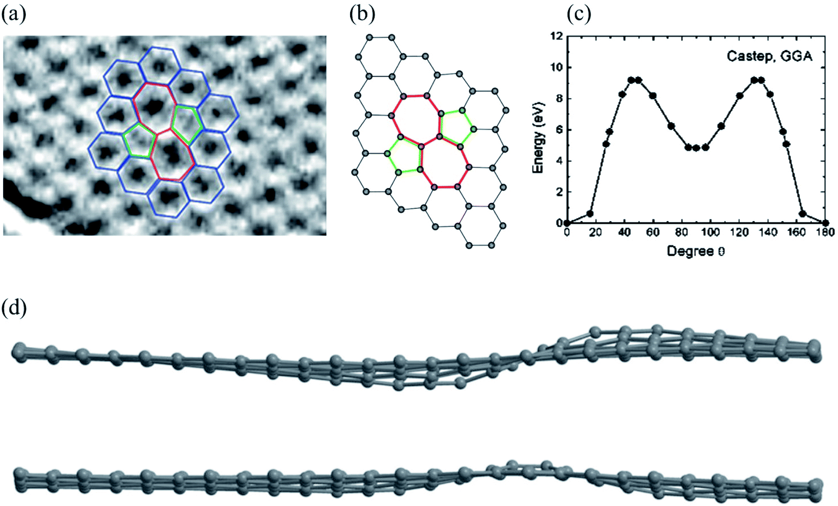 | ||
| Fig. 1 Stone–Wales defect SW (5775): (a) experimental TEM image. Reprinted from ref. 113. Copyright 2008 American Chemical Society; (b) DFT calculated image. Reprinted from ref. 26. Copyright 2010 American Chemical Society; (c) DFT calculated energy barrier for bond rotation. Reprinted from ref. 64. Copyright 2005 American Chemical Society; (d) DFT calculated image of sine and cosine like configurations. Reprinted from ref. 118. Copyright 2015 Pleiades Publishing Ltd. | ||
The SW defect has a calculated penetration barrier below 1 eV and an H+-over-D+ selectivity of 7 at room temperature, while hydrogenation also reduces the penetration barrier with significantly lower isotope selectivity.127 A carbon vacancy and the SW defect play significant roles in the observed p-type behavior, changes in electrical or optoelectronic characteristics, and degradation of graphene under ambient gases (N2, O2, Ar, and CO2) or atmospheric oxygen.128 The single vacancy and SW defects could decrease the current through the graphene nanodevices using the ballistic transport model, accompanied by defect-induced electron transmission peaks,129 signifying that this method can hopefully be used to study the influence of multiple vacancy chains on the electronic transport properties of graphene nanodevices.130 For the zigzag-direction loading, slip nucleates in the SW defect through the formation of two pentagons and a twisted hexagon. In contrast, for the armchair-direction loading, healing, generation, and pentagon–heptagon pair separation of the SW defect occur via 90° rotation of the C–C bond.131 There are two distinct orientations of the SW defects, namely, types I and II, caused by the 90° rotation of the C–C bond in different directions. Ebrahimi et al.132 studied the effects of the orientations and concentrations of the SW defects on the thermal conductivity of zigzag and armchair GNRs using the reverse nonequilibrium molecular dynamics method. It is found that the thermal conductivity of GNRs with two different chirality cases reaches its minimum in the range of 0.1–0.7% defect concentration, with more significant thermal conductivity of zigzag GNRs with type II defects than the GNRs with type I defects at high concentrations of the SW defects.
The SW defect in graphene is expected to modify its vibration and be seen in its Raman spectrum. The introduction of SW defects in graphene is also expected to affect the mechanical properties of graphene. Molecular dynamics (MD) simulations predicted that SW defects dramatically reduce the strain failure and the intrinsic strength of the monolayer graphene sheet. The SW defects in graphene can modify its physical properties and change its chemical properties by acting as active sites for the adsorption of other atoms and molecules and increasing the local chemical reactivity. DFT calculations predicted that SW defects in graphene strongly influence hydrogen chemical reactivity.133 Similarly, SW defects in graphene can enhance the adsorption of Li, Na, K, and Ca atoms because of better electron transfer between the adatom and the defective graphene sheet. Therefore, SW defects in graphene are much more suitable for its use in transistors, hydrogen storage, and high-capacity anode material in metal (Li, Na, K, and Ca)-ion batteries.62,134–138
2.2 Single vacancy defects
A single vacancy (SV) in graphene is generated by missing a single carbon atom. Previous experimental and theoretical studies have observed single vacancies (SV) in graphene using TEM112,113 and STM.49,139,140 Fig. 2 shows a TEM image of the single vacancy defect and the corresponding atomic model.26,114 Because of the Jahn–Teller distortion, two of three dangling bonds are saturated and pointed towards the missing atom. One of them always remains because of geometrical reasons. The monovacancy with such a dangling bond requires higher formation energy of 7.5 eV than the Stone–Wales defect, and the corresponding migration barrier is ∼1.3 eV at 100–200 °C.84,141 Many theoretical studies have been devoted to the diffusion of vacancies and the structural changes produced in graphene.49,85,142 The magnetic moment arising from an SV is attributed to the presence of unpaired electrons created by removing a carbon atom.85 DFT calculations for an SV showed that the presence of the vacancy produces a pentagon-like structure because of the formation of a weak covalent bond between two atoms surrounding the vacancy. Among the three dangling bonds, the third bond plays a vital role in creating the magnetic moment of about 1.04 μB in pure nonmagnetic graphene.85 The experimentally determined magnetic moments of graphene with vacancies and traces of room temperature ferromagnetism are still disputatious and debatable.143–146 Valencia et al.147 predicted a magnetic moment of 2 μB for the SV in graphene. They found that periodic arrays of single vacancies may provide interesting spin–spin interactions because of the specific symmetry of the graphene lattice. Kim et al.148 studied the effect of vacancies and tensile strain on the quality factor for mass sensing using graphene monolayers with an SV at the center. Therefore, the effect of multiple SVs and their randomly distributed positions on graphene nanosheets' performance needs more consideration. Graphene sheets in zigzag and armchair directions exhibit slightly different Young's moduli ranging from 1.20 to 1.10 TPa in the zigzag direction and from 1.12 to 1.09 TPa in the armchair direction using continuum modeling.149 Repeating vacancy or divacancies in GNR induce metallization and magnetization in nonmagnetic semiconducting nanoribbons because of the spin polarization of local defect states. The antiferromagnetic ground state of semiconducting zigzag ribbons can change to a ferrimagnetic state upon creating vacancy defects.113 Defects significantly influence the mechanical properties of graphene. Wang et al.150 investigated the mechanical behaviors of defective graphene sheets with vacancies using MD simulations. They found that vacancies cause a considerable loss of strength, and the fracture strength is sensitive to the loading directions and temperature. | ||
| Fig. 2 Single vacancy defect in graphene: (a) experimental TEM image. Reprinted with permission from ref. 113. Copyright 2008 American Chemical Society and (b) atomic structure as obtained from DFT calculations. Reprinted with permission from ref. 26. Copyright 2010 American Chemical Society. | ||
Carpenter et al.151,152 reported the vacancy-induced amorphization and the mechanical properties of irradiated single-layer graphene using MD simulations. They found a critical range of vacancy concentrations, leading to a qualitative change in the fracture response from brittle to ductile. The fracture strength of graphene is lost by about 17.7% because of a single vacancy. Despite the recent progress, little is known about the evolution of defective graphene morphology during tension.153 SV and SW defects can be created when rapid quenching occurs or when the graphene is irradiated. Some researchers have extensively investigated these defects.65,154,155 A recent study has determined that the activation energy for the diffusion of a single vacancy in graphene is extremely sensitive to in-plane uniaxial strain, both parallel and perpendicular to the direction of the hopping motion of a single vacancy, with the barrier doubled or halved with a respective tensile or compressive strain of just 2–3%55,156 in applications of investigating the elastic properties of graphene.
2.3 Multiple vacancy defects
Double vacancy (DV) means either coalescence of two single vacancies (SVs) or removal of two neighboring carbon atoms. DV can be reconstructed, resulting in two pentagons and one octagon labeled the 5–8–5 defect. Fig. 3 shows the atomic structures of divacancies obtained by DFT and experimental TEM images.157 Previous studies reported the formation energy of about 8 eV for DV, which is 4 eV per atom, comparatively less than that of an SV.84,141 It means that the DV is energetically more stable than the SV. In the presence of dangling bonds, the material becomes very unstable and tends to chemically bond with impurity atoms or molecules. The SV defect causes a dangling bond, whereas the 5–8–5 defect causes only local deformation. As a saturated eight-membered ring compound, a cyclooctane molecule, (CH2)8, also has a non-planar structure that looks like a crown or a boat. Since the 5–8–5 defect also has a considerable local curvature, the system is changed to the 555–777 or 5555–6–7777 defect to reduce the local curvature. Therefore, all three defect structures can be found when observed with TEM, as shown in Fig. 3. The defect transformation will be described in detail later. | ||
| Fig. 3 DV defects in graphene. (a–c) Atomic structures obtained from DFT calculations. Reprinted with permission from ref. 157. Copyright 2016 IOP Publishing. (d–f) Experimental TEM images corresponding to the atomic models in (a–c), respectively. Reprinted with permission from ref. 26. Copyright 2008 American Chemical Society. Here, (a and d) the 5–8–5 defect, (b and e) the 555–777 defect, and (c and f) the 5555–6–7777 defect. | ||
Removing more than two carbon atoms, known as multiple vacancy defects, may lead to larger and more complex defect configurations. In this regard, one would expect to observe a more-or-less random set of vacancies. Therefore, it seems possible for the lattice to reconstruct locally around the vacancies and form a random set of non-hexagonal polygons. Two pentagons and one octagon appear for a fully reconstructed double vacancy, leading to no dangling bond. A collaborative experimental and theoretical study of graphene divacancy revealed a non-hexagonal rearranged flat structure with no magnetic traces.158 The divacancy (DV) and larger vacancies could be frequently created by the current physical and chemical treatment, even though the SV has been more widely studied.50,159–162 TEM results indicate that multiple vacancies, rather than monovacancies, are produced more easily under electron irradiation conditions.111 Theoretical calculations at different levels of theory also point out that the formation energies of the DV in carbon nanotubes and graphene are much lower than monovacancy (SV) formation energies.57,87,141,163,164 The presence of more than one vacancy and their mutual relationship significantly alters the magnetization phenomenon in graphene because of the creation of sublattice imbalance.75,165,166 Wang et al.130 systematically investigated the electronic transport properties of various defects in graphene, such as SW defect, SV, DV, and multiple vacancy chains using first-principles calculations combined with the non-equilibrium Green's function method. They found that some defect-induced electronic states can enormously enhance the transport of electrons between electrodes at certain energy levels. In contrast, others are only localized around the defect sites and could be identified using a small source-drain voltage and sweeping the gate voltage applied to the graphene field-effect transistors.
Lee et al.57 reported the spontaneous reconstruction and transformation of the 5–8–5 defect into a more stable form of the 555–777 defect consisting of three pentagon/heptagon pairs. Kim et al.75 also studied the same transformation and reported that the activation energy barrier of the change of 5–8–5 into 555–777 defect was around 5.3 eV. Cretu et al.167 showed that the formation energy of the 5555–6–7777 defect (formed by a bond rotation from the 555–777 of 30° for the graphene sheet and consisting of four pentagons and four heptagons recently observed in a few TEM experiments58,168) lies in between that of forms 5–8–5 and 555–777. The rotation barrier is around 6 eV. All these migration steps are undoubtedly interesting in understanding the behavior of defects in graphene, but the picture is still probably quite incomplete.
Recent studies have revealed that multiple vacancies in graphene can create substantial and inhomogeneous displacement strain that extends far into the surrounding lattice. This is caused by the reconstruction induced by the pair-wise removal of dangling bonds.66,108,169–171 Moreover, in a regular arrangement, multiple divacancies can form chain-like line defects, known as extended line defects (ELDs). Four types of extended line defects (5–8–5, 55–77, and 555–777 defects for armchair GNRs, 48 defects for zigzag GNRs) were mainly observed in experiments,58,172 and the formation of chain structure could be controlled precisely.69 The influence of the 5–8–5, 55–77, and 555–777 ELDs on the thermal transport properties of the armchair graphene nanoribbon was also reported.173
2.4 Carbon adatom defects
When a carbon adatom is adsorbed on a defect-free graphene sheet, forming two covalent C–C bonds between the adatom and the underlying carbon atoms in the graphene sheet, the adsorption energy of the C adatom is about 1.5–2.0 eV with the migration barrier of ∼0.4 eV.174,175 The adsorption position of the C adatom is a bridge site between two carbon atoms in the graphene sheet.176 Since the triangular structure caused by the adsorbed carbon atom is unstable, the adsorbed atom moves quickly on the graphene surface with a high-speed migration rate. Therefore, it is challenging to capture the C adatoms using microscopic techniques such as TEM, STM, etc. There is no relevant research on the experimental observation of carbon adatoms on the graphene surface. However, based on the earlier studies on the activation mechanism of activated carbon, carbon and oxygen atoms can migrate on the surface of the carbon layer. Therefore, the existence of out-of-plane carbon adatoms can be confirmed. On the other hand, carbon adatoms are generated under electron irradiation in aberration-correlated transmitted electron microscopy (AC-TEM) or as contaminants in the growth of graphene.111,177,178 The adatoms are viewed to form a bridge-like structure on the graphene surface under TEM,111 and bridging atoms can be found in reconstructions of vacancies (odd vacancies).177 Such adatoms can catalyze the formation and dissociation of bonds in graphene because of their undercoordination for bulk sp2 carbon atoms. Still, their precise role and observation in common compound defects in graphene remain unclear.179 Ataca et al.180 investigated the adsorption of carbon adatoms on graphene and its nanoribbons using DFT methods. They found that carbon adatoms prefer to adsorb to the bridge sites and modify graphene's electronic and magnetic properties. The adsorption site geometry with carbon adatom and charge density contour plots in the lateral plane and a vertical plane (perpendicular to the x-axis) are shown in Fig. 4a–d. Band structures and corresponding density of states calculated for a 2 × 2 supercell are demonstrated in Fig. 4e. The binding energy was the maximum at the bridge site (Fig. 4a). The top site adsorption was observed with a local minimum of 0.3 eV higher energy (Fig. 4b). The C–C bond elongated below C′, and its charge was slightly delocalized (Fig. 4c and d). The charge density analysis indicated that the orbitals of C′ are combined with π and π* orbitals of bare graphene, forming new bands near the Fermi level (Fig. 4e). The flat band driven from perpendicular sp2 orbitals was filled and gave rise to a peak at an energy of ∼2 eV below the Fermi level in the total density of states. Bands generated from hybridizing other sp2 orbitals of C′ with the π and π* states of graphene occurred near the Fermi level and attributed a metallic character. The band above The Fermi level was generated because of an antibonding combination of p-orbital of C′ perpendicular to the C–C′–C plane and π* states of graphene. Wang et al.124 investigated the adsorption of carbon adatoms in graphene via a mechanically different process. They found a relatively tiny restoration barrier of about 0.87 eV using DFT methods, which could make the SW-healing experimentally accessible. Subsequently, the C-adatom can migrate very quickly on the graphene surface. They claimed that their proposed carbon-adatom catalytic mechanism played a crucial role in healing the SW defect during the growth of graphene.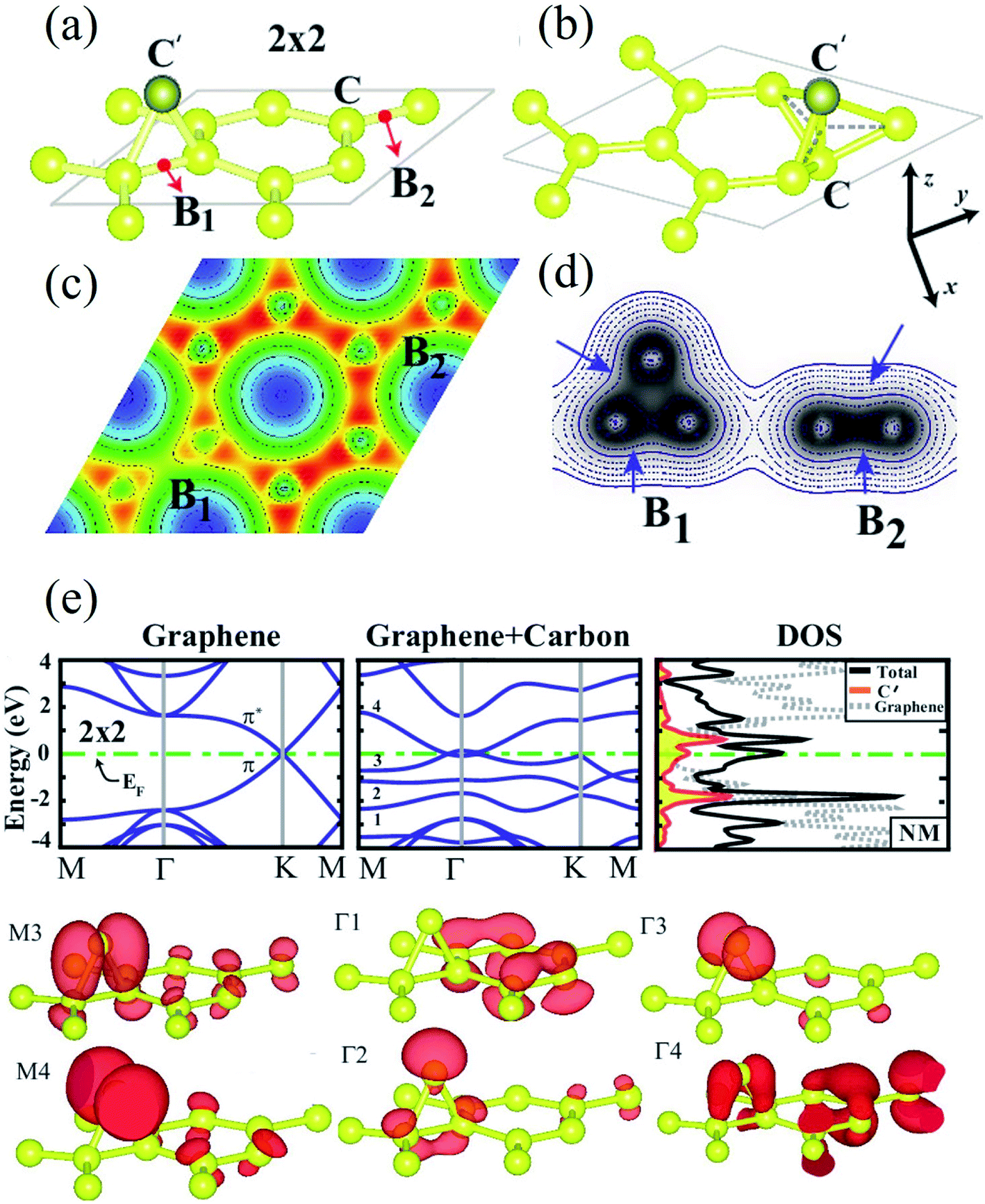 | ||
| Fig. 4 (a) The bridge site bonding geometry of carbon adatom C′; (b) adsorption geometry of carbon adatom C′ at the top site; and (c) charge density contour plots in the (x, y) plane as well as (d) in a vertical plane (perpendicular to the x-axis) for bridge site bonding. (e) Band structures and corresponding density of states calculated for a 2 × 2 supercell. Reprinted with permission from ref. 180. Copyright 2011 American Institute of Physics. | ||
Zhang et al.157 reported that a developed three-center tight-binding model for carbon181 exhibits excellent band structures, binding energies, and other properties of various carbon crystalline structures and surfaces in excellent agreement with first-principles calculations and experimental results available in the literature. They also searched for the stable forms of vacancies and embedded atoms of various sizes and made systematic calculations to understand better the stable structures and energies of various vacancy and embedded-atom defects in graphene. Consequently, the structural change during the initial stages of activation will help tune the processing of such out-of-plane carbon adatoms to different applications for molecular sieving,182 gas storage,183 catalysis,184 hydrogen storage,185 and lithium-ion batteries.186
2.5 Foreign adatom defects
During the process, metal atoms or oxygen-containing functional groups are incorporated into the surface of graphene during the CVD or by a strong oxidation method. The effect of a foreign (noncarbon) adatom on graphene properties depends on the bonding between the adatom and graphene. Such impurity atoms on the graphene layer are bonded with the nearest carbon atoms with covalent bonding or weak van der Waals interaction.187 Dispersive forces increase the adsorption strength by 0.35 eV. Because the bond between foreign impurity atoms and graphene is weak, the impurity atoms can move on the graphene surface.167,188,189 However, few experimental studies have reported the migration of foreign impurity atoms.Low migration barriers in the range of 0.2–0.8 eV have been found in theoretical investigations, implying high adatom mobility at room temperature.190 Many researchers have performed DFT calculations of the adsorption of various metal atoms191–205 to investigate energetically stable adsorption sites and their effects on graphene's structural, electronic, and magnetic properties. When Au atoms are bonded to graphene, electrons are transferred from graphene to Au atoms, making the graphene p-doped. When the other transition metal (TM) atoms are attached to graphene, electrons are transferred from the TM atoms to the graphene, and the graphene becomes n-doped. Early TM atoms show significant magnetism to graphene since fewer than five electrons are filled in the d shell. In contrast, the local magnetic moments of late TM atoms with more than five electrons in the d shell decrease.206 The work function of metal-doped graphene falls with increasing metal adatom concentration and becomes saturated at specified values. The saturation values of the work function for Cs-, Rb-, K-, Na-, and Li-doped graphene sheets were 2.05, 2.18, 3.24, 2.42, and 2.49 eV, respectively. When electrons move from the metal dopant to the clean graphene, the graphene becomes n-doped, and the Fermi energy rises above the Dirac point for all metal atoms investigated. Then, the work function is significantly reduced.207,208
Recent experimental studies on graphene have focused on the interaction of transition metals with graphene on the atomic scale, and various experimental tools have been utilized.188,209–214 One of the important tools to probe the resonant effects between graphene and metal nanoparticles (NPs) is surface-enhanced Raman spectroscopy (SERS). Significant Raman enhancements for various laser excitations have been reported due to near-field plasmonic effects near metal NPs and graphene.215,216 Urich et al.209 studied the enhanced electron–phonon interaction by monitoring the surface plasmon resonance effect in the Ag–graphene hybrid structure. Park et al.217 investigated the Au NPs–graphene–Au film junction (hybrid system) to identify the layer breathing mode and other out-of-plane phonon modes of few-layer graphene through SERS. Zandiatashbar et al.72 utilized a modified oxygen plasma technique to incorporate defects in pristine graphene in a controlled fashion. They also used Raman spectroscopy and transmission electron microscopy to characterize the defects, then used AFM nano-indentation to quantify the stiffness and strength of defective graphene experimentally. Finally, they theoretically used finite element modeling and molecular simulations to understand such behavior. They found graphene sheets with defects were more rugged and structurally robust than previous results. Very sensitive thermal and electrical transport in graphene is observed for disruptions in the sp2-bonding network. One significant result is that defective graphene's breaking strength is only 14% smaller than its new counterpart in the sp3-defect regime.
Meanwhile, understanding the role of Cu vapor in the graphene growth process is essential to developing a reliable synthesis method for high-quality graphene. However, only a few studies218,219 examined the effects of Cu vapor on graphene growth. Lee et al.220 investigated the effects of Cu vapor on the growth of CVD graphene on a Cu surface. They found that the high partial pressure of Cu vapor enlarges the graphene grains by reducing the surface concentration of the carbon adatoms that participate in graphene growth. Also, the presence of Cu vapor favors the selective etching of oxygen functionalized carbons in graphene, thus increasing the efficiency of healing graphene defects by CH4. They claimed a higher charge carrier mobility of 14![[thin space (1/6-em)]](https://www.rsc.org/images/entities/char_2009.gif) 700 cm2 V−1 s−1 than exfoliated graphene by continuously supplying Cu vapor during CVD. Since adatoms' properties are highly dependent on the adsorption configuration (e.g., isolated vs. clustered), it is essential to understand these effects (configuration-dependent properties and migration) from a theoretical perspective and be able to test them experimentally.
700 cm2 V−1 s−1 than exfoliated graphene by continuously supplying Cu vapor during CVD. Since adatoms' properties are highly dependent on the adsorption configuration (e.g., isolated vs. clustered), it is essential to understand these effects (configuration-dependent properties and migration) from a theoretical perspective and be able to test them experimentally.
2.6 Substitutional impurity defects
Substitutional impurities can be generated by incorporating foreign atoms so that the removal of a carbon atom creates a vacancy filled by a foreign atom. Substitutional doping of graphene is an efficient and widely used method to tailor graphene's electronic and magnetic properties. Foreign atom impurities are either metal or non-metal elements. In this case, the impurity atoms replace one, two, or more carbon atoms. For non-metal impurities, boron or nitrogen atoms are of considerable interest because impurities shift the position of the Fermi level and change the electronic structure of graphene.133 Nitrogen and boron are commonly used as electron donors or acceptors in graphene because their atomic sizes are closer to carbon and readily fit the graphitic lattices.221,222 The covalent bonds between the N or B atoms and neighboring C atoms ensure that doped graphene possesses long-term thermal and chemical stability. On the other hand, the migration of Au and Pt atoms, most likely at substitutional sites in graphene layers, has been the subject of an in situ study by electron microscopy.188 Substitutional defects have been found in transition metal dichalcogenides in the electron beam irradiation process by introducing other atomic species into the TEM chamber. The local density of states shows that N, P, As, and Sb atoms behave as acceptors, whereas F, Cl, Br, and I atoms are likely to be donors. The isoelectronic atoms, such as O, Se, or Te atoms, did not produce any localized states, signifying that they could heal the electronic structure of transition metal dichalcogenides with chalcogen vacancies.223Both experimental and theoretical studies reported that the heteroatoms (N, B, or S) could modify the electrical properties of graphene with efficient catalytic properties for oxygen reduction reaction (ORR) because of the polarized distribution of spin and charge densities by doped heteroatoms.34,224–230 Because DFT is an effective method for studying the electronic properties of catalytic materials and ORR mechanisms, it was used to investigate the ORR mechanisms in various catalytic materials.231–233 The ORR mechanisms on carbon-supported Fe or Co-phthalocyanine in alkaline media were also investigated. Prof. Lv and Prof. Yamada nicely explained nitrogen in graphene and graphene nanoribbons.234–236 In particular, Prof. Lv shows a nice microscope image of the nitrogen-containing defects.234 In the literature, Prof. Yamada summarizes the types of oxygen-and nitrogen-containing functional groups.235–237 Chen et al.238 performed DFT calculations to study the ORR mechanisms on graphene, nitrogen-doped graphene, and cobalt–graphene–nitride systems.232,239 Bhatt et al.43 comparatively investigated the ORR mechanisms on Al-doped X-graphene (X = N, P, and S) electrocatalysts in the acidic medium in a fuel cell cathode. They found that Al-doped N- and P-graphene sheets are energetically more favorable than Al-doped S-graphene catalysts for enhanced and stable ORR via four-electron transfer pathways in an acidic environment. Prof. Nakamura and Prof. Ozaki also investigated ORR in nitrogen-doped carbon materials for fuel cell applications.240–243 Using STM, Zhao et al.244 reported images of individual nitrogen atoms doped in monolayer graphene. Measurements using X-ray photoelectron spectroscopy and near-edge X-ray absorption fine structure spectroscopy confirmed the presence of N dopants in graphene lattices as well as the formation of in-plane N–C bonds, indicating that the nitrogen atoms were substituted into the graphitic matrix. STM images (Fig. 5a) and simulations (Fig. 5b) reveal that a fraction of the extra electrons of the nitrogen atom delocalized into the graphene lattice, leading to the triangular shape of the individual N dopant sites. Because STM is sensitive to DOS near the Fermi level, resolving the atomic structure of topological defects involving delocalized electrons remains difficult. Marangoni et al.245 synthesized an N-doped chevron GNR (cGNR) decorated alternatively with electron-rich carbazole groups (pentagon) and electron-deficient phenanthridine (hexagon) at the convex protrusions of the cGNRs, as shown in Fig. 5c and d. Previous research found substitutional Ni impurities in single-walled carbon nanotubes (SWCNT) and graphitic particles.246 Ushiro et al.247 reported that Ni substitutional defects are present in SWCNT samples even after careful purification. According to their analysis of the X-ray absorption data, the most likely configuration was the one in which the Ni atom replaces a carbon atom, as shown in Fig. 5e,41 and four nitrogen doping configurations usually observed on graphene catalysts.248
 | ||
| Fig. 5 Substitutional doping of graphene and graphene nanoribbons: (a) STM image of graphene on copper foils with a single graphitic N dopant and (b) simulated STM image of graphene with a single graphitic N dopant. Reproduced with permission from ref. 244. Copyright 2011 American Association for the Advancement of Science; (c) schematic of nitrogen-doped chevron GNR with highlighted carbazole (yellow) and phenanthridine (orange)rings and (d) Nc-AFM image of a cGNR on Au (111) with the phenanthridine and carbazole groups highlighted with yellow and orange rings. Reproduced with permission from ref. 245. Copyright 2016 Wiley-VCH; (e) typical geometry of transition 3d, 4d, and 5d substitutional metal atoms in graphene. Reproduced with permission from ref. 41. Copyright 2016 Royal Society of Chemistry; (f) four nitrogen doping configurations usually observed on graphene catalysts. Reproduced with permission from ref. 249. Copyright 2018 https://www.mdpi.com/journal/catalysts; (g) HRTEM images of pristine graphene and oxidized graphene after 5 hours of oxidation at 493, 513, and 533 K. Reproduced with permission from ref. 250. 2014 American Chemical Society; (h) side views of relaxed structures of a single TM (M = Fe, Co, Ni, or Cu) atom and TM (M1 or M2 = Co, Fe, Ni, or Cu) pairs with antisymmetric and symmetric forms. C or N atoms are represented by blue balls in the schematic diagram. Reproduced with permission from ref. 248. Elsevier Ltd. 2021 Copyright. | ||
Substitution of magnetic transition metals is also expected to strongly affect the magnetic properties of graphene nanostructures. For example, transition metals like Fe, Ni, or Co are among the most common catalysts used to produce SWCNT.249 Rodriguez-Manzo et al.251 also investigated the possibility of creating individual vacancies at desired locations in carbon nanotubes using electron beams. When combined with the observed stability of substitutional impurities, such an ability may provide a route to fabricating new devices incorporating substitutional impurities in certain locations or arranged in particular ways. Si impurities can further pick up various atoms from the environment. Recent experimental studies have reported the presence of individual defects formed by the occurrence of silicon and nitrogen impurities.252,253 Zhou et al.252,253 showed that surface plasmons are locally enhanced at silicon and silicon-nitrogen impurities. Therefore, in principle, such silicon impurities in graphene could be used as plasmonic waveguides with potential applications in optoelectronic devices.254 Electronic transport in systems with silicon point defects has been studied in ribbon geometry.255 In addition, Cheng et al.256 studied the electronic and transport properties of the SiNx defects in armchair nanoribbons. However, it is unclear about the transport properties of realistic two-dimensional graphene systems with numerous randomly positioned defects. Ervasti et al.257 reported that many nitrogen-doped silicon impurities exhibited finite spin moments with graphene-based spintronics applications and evaluated the spin-dependent electronic and transport properties of the most stable defects. The doping of graphene with transition metals and their spintronics applications is underway. Thus, the study of magnetic substitutional impurities is vital for a theoretical understanding of magnetism for atomic defects in graphene and for explaining experiments in progress that dope graphene with elements of the traditional magnetic bulks (Fe, Co, and Ni). Previously, substitutional 3d transition metal atoms in a graphene layer were computed, and a simple model was proposed to explain their bonding and magnetism.190,258 Some researchers claimed that the ORR active sites are the M–Nx impurities in M–Nx/C catalysts.259,260 He et al.261 reported the performance of MNx/C in the order of FeNx/C < CoNx/C < NiNx/C < CuNx/C.260,262 They suggested that O2 and OH adsorption energies represent the ORR catalytic activity and stability for MNx/C electrocatalysts. Zhang et al.263 performed both experimental and DFT investigations on transition metal (Fe, Co, Ni, Cu) phthalocyanines as electrocatalysts for ORR and concluded O2 and OH adsorption energies as the catalytic activity and stability, while H2O2 desorption energy as the number of electrons transferred in ORR processes. Bhatt et al.264 performed DFT calculations to investigate the ORR mechanisms on M–N2–G (M = Ti, Cu, Mo, Nb, and Ru) catalysts and found that M–N2–G (M = Ti, Cu, Mo, Nb, and Ru) catalyst surfaces are energetically favorable (exothermic) for ORR through 4-electron transfer pathways to form two water molecules. However, the Cu–N2–G catalyst surface facilitates the formation of unwanted hydrogen peroxide through two-electron transfer pathways. Li et al.265 very recently investigated both the ORR and oxygen evolution reaction (OER) catalytic activities of zinc and nitrogen co-doped graphene with different zinc–nitrogen (Zn–N) coordination numbers and configurations and found that both Zn–N coordination numbers and structural configurations influence the ORR and OER activities on ZnNx sites. They concluded that the O-p orbital shows moderate hybridization strength with the N-p and Zn-d orbitals in O-adsorbed ZnN4 systems, thus facilitating electrocatalytic reactions. The vacancy defects have been introduced by heat-treating graphite oxide253 and graphene under oxygen in the literature.254 A schematic diagram of single and two metal atoms on graphene is shown in Fig. 5h.248 Li et al.266 investigated a metal-defect-free electrocatalyst-driven oxygen reduction reaction in acid electrolyte using experimental and computational methods. Their results reveal that the pentagonal S defect is essential for the ORR in acidic electrolytes because it remarkably increases reactivity. One graphitic-type N in the meta-position of the pentagon defect further significantly improves the reactivity due to locally precise control of the electronic structure, thus forming highly active sites for ORR in acid. Fig. 6 shows the synthesis process and the morphology with active sites.266
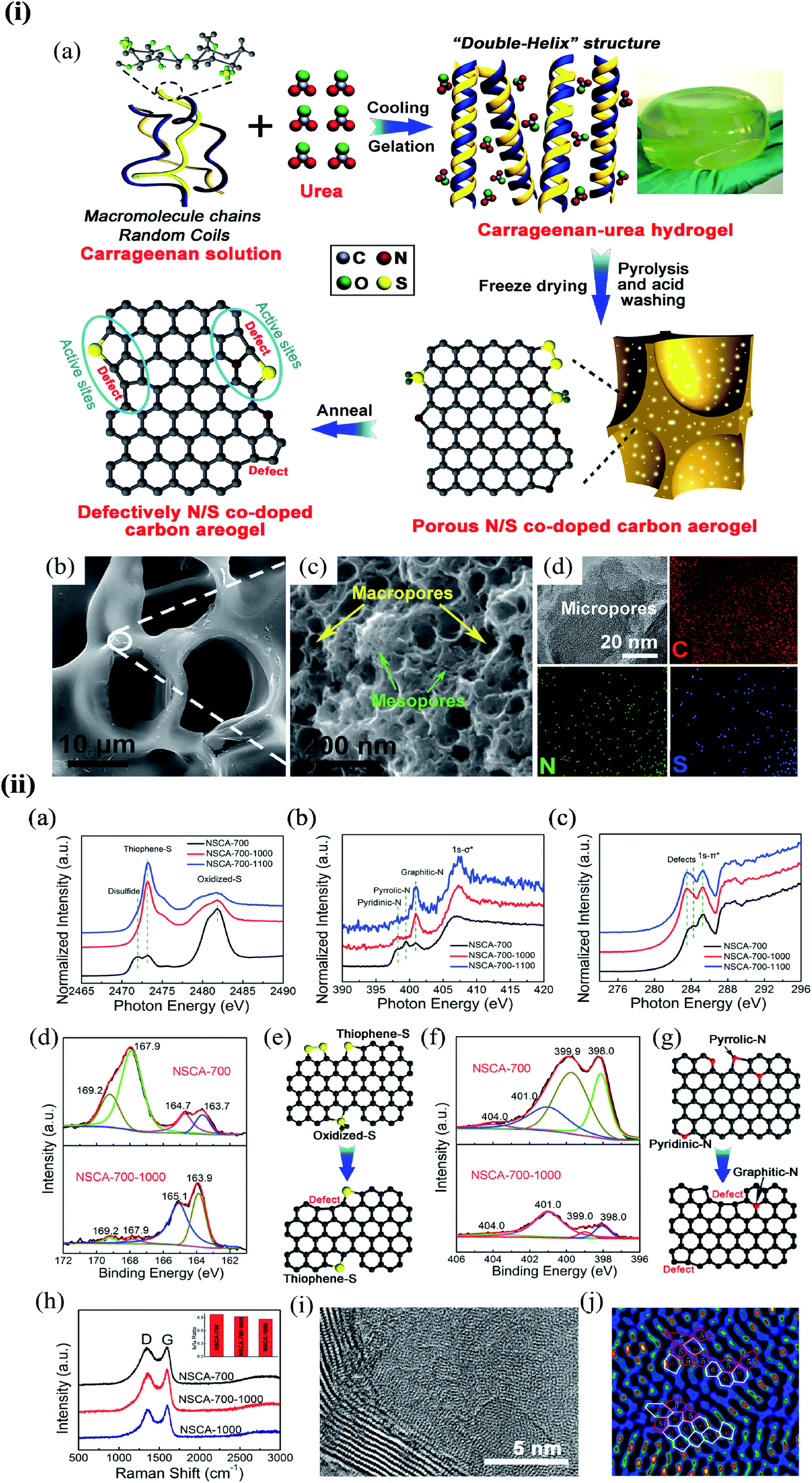 | ||
| Fig. 6 (i) The synthesis process and morphology of N-modified S-defect carbon aerogel: (a) schematic illustration of the synthesis process; (b and c) low-resolution (b) and high-resolution (c) FESEM images of NSCA-700-1000 and (d) TEM image and the corresponding EDS mapping for C, N, and S elements of NSCA-700-1000. Reprinted with permission of ref. 266. Copyright 2018 Elsevier Inc. (ii) Characterization of NSCA: (a–c) S K-edge (a), N K-edge (b), and C K-edge (c) XAS spectra of NSCA-700, NSCA-700-1000, and NSCA-700-1100. (d and f) The high-resolution XPS spectra of NSCA: (d) S 2p and (f) N 1s. (e and g) Schematic illustration of the conversion of the heteroatom dopant through annealing treatment: (e) S dopant and (g) N dopant. (h) Raman spectra of NSCA-700, NSCA-700-1000, and NSCA-1000. (i and j) STEM (i) and the corresponding filtered images (j) of NSCA-700-1000. Reprinted with permission of ref. 266. Copyright 2018 Elsevier Inc. | ||
A schematic illustration of the synthesis process is shown in Fig. 6i(a). Field emission scanning electron microscopy (FESEM) images show that all the samples have a 3D self-supporting core network structure (Fig. 6i(b). Small-sized macropores and mesopores with interconnected structures can be observed in the wall of the network (Fig. 6i(c) NSCA-700-1000)), delivering a large specific surface area. The porous structure and high surface area can supply a high density of exposed active sites and promotes mass transport. Transmission electron microscopy (TEM) – energy dispersive X-ray spectroscopy (EDS) elemental mappings show that the doped S and N atoms partially remain in the carbon aerogels after annealing at 1000 °C (Fig. 6i(d)). S K-edge X-ray absorption structure (XAS) spectra indicate that NSCA-700-1000 and NSCA-700-1100 mainly contain thiophene S as the dibenzothiophene-like structure (2473.3 eV). Oxidized S (2481.8 eV) and disulfide (2472.0 eV) structures in NSCA-700 were removed or transformed into thiophene S (Fig. 6ii(a)).
2.7 One- and two-dimensional defects (topological defects)
The concept of dislocations is based on 1D line defects. Grain boundaries or stacking faults are 2D defects. Besides, various types of edge terminations exist in 2D materials, and applying strain can also modify the structure of graphene. Such defects in the bilayer and multilayer graphene are also essential. A one-dimensional defect has been observed in several experimental studies of graphene.72,73 Some of them in graphene resemble dislocations in a conventional crystal. However, the traditional concept requires a Burgers vector and a dislocation line, which only appear in a three-dimensional crystal.1 Various 1D or 2D defects will be discussed in the following sessions.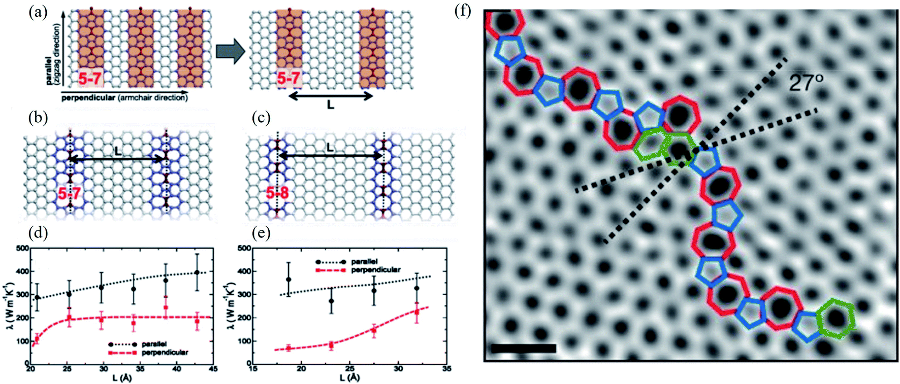 | ||
| Fig. 7 Effect of line defects on thermal conductivity of a graphene monolayer: (a) arrangement of 5–7 defect lines; equilibrium structures of (b) 5–7 and (c) 5–8 defect lines; thermal conductivity λ of the system with (d) 5–7 and (e) 5–8 line defects as a function of their separation L at T = 300 K. Reproduced with permission from ref. 276. Copyright 2014 American Physical Society. (f) Aberration-corrected annular dark-field scanning transmission electron microscopy (ADF-STEM) of line defects in graphene; scale bars: 5 Å. Reprinted with permission from ref. 269. Copyright 2010 Nature Publishing Group. | ||
Line defects, including grain boundaries and wrinkles, are commonly seen in graphene grown by CVD, which is believed to alter the graphene's electrical and mechanical properties. Unfortunately, it is challenging to directly distinguish grain boundaries from wrinkles because of their similar morphologies. Long et al.277 reported high-resolution Kelvin potential force microscopy (KPFM) to measure the work function distribution of graphene line defects and found the different work functions of grain boundaries, standing-collapsed wrinkles, and folded wrinkles. They concluded that the unique work function distribution of each type of line defect originated from the doping effect induced by the SiO2 substrate using classical and quantum molecular dynamics simulations. Ramiro Marcelo dos Santos et al.278 recently investigated the effects of the different numbers of line defects of substitutional nitrogen or silicon atoms on the penta-graphene electronic behavior. They found that such doping can induce semiconducting, semi-metallic, or metallic behavior depending on the doping atom and targeted hybridization (sp2 or sp3-like carbons). They concluded that nitrogen doping of sp2-like carbon atoms could produce a bandgap modulation between semi-metallic and semiconducting behavior.
Recent STM measurements have shown that the o–p line defect exhibits excellent electronic properties.69,279 However, its mechanical properties are largely unknown.280 Substitutional nitrogen doping has been done via CVD or electrochemical treatment.281–283 The effect of nitrogen doping on the electronic properties of pristine or point-defected graphene has been widely studied from both the experimental and computational sides [241, 311–313].221,283–286 However, few studies have addressed doping in extended line defects.287,288 Brito et al.288 have shown that nitrogen doping is more favorable near a line defect than in the graphene region based on formation energies using DFT. Berger et al.289 addressed the effects of nitrogen and boron doping on the electronic and mechanical properties of h–p and o–p line defects in graphene employing full-potential DFT by investigating the fact that doping primarily affects the occupation of the frontier orbitals, i.e., occupation through n-type doping or local substitution with nitrogen increases the ultimate tensile strength remarkably. What will happen in the presence of two or more line defects? Motivated by finding an efficient realization of the high valley polarization, Liu et al.290 studied the electron transmission coefficient in the presence of several line defects. They discovered a noticeable change in transmission coefficients with varying distances between two-line defects with temperature insensitivity. Polarization could be used for information processing much as the electron spin degree of freedom is used in spintronics, with the added benefit of temperature insensitivity. Two methods have been suggested for lifting the degeneracy and thus achieving graphene valley polarization: (i) by applying an external magnetic field and (ii) by modifying the lattice. The first method requires very high magnetic fields and low temperatures or optical pumping by circularly polarized light to generate and detect valley polarized currents. The second method is more compatible with modern electronic synthesis but requires a practical way of generating functional atomic-scale structures and a compact scheme for operating the device.291–297
Remarkably, extended line defects induce charge redistribution in their surroundings and could thus behave as a metallic wire embedded in a graphene sheet.69 As a result, when compared to isolated defects associated with electron scattering and heat generation,298 such topological defects may improve graphene's electronic transport properties.107,279,280,299 However, these properties generally depend on the relative orientation between the grain boundary and transport direction.300–302 It was shown that the interaction between graphene and electron acceptor molecules increases the device's conductivity. In contrast, electron donors induce a decrease in conductivity, which has also been experimentally observed for various molecules.303–308 Nonetheless, the interaction between graphene and closed-shell molecules tends to be relatively weak, implying a low signal-to-noise ratio. Zhang et al. investigated whether the sensitivity of graphene-based nanosensors could be improved by introducing dopants or vacancies.309,310 However, such an improvement to graphene-based gas sensors comes at the cost of significantly larger adsorption energies of the target molecules and, consequently, an increase in recovery time. Hence, a suitable sensor should have three essential features: (i) a small but not negligible binding energy, (ii) significant sensitivity, and (iii) significant selectivity to different gases.311–313
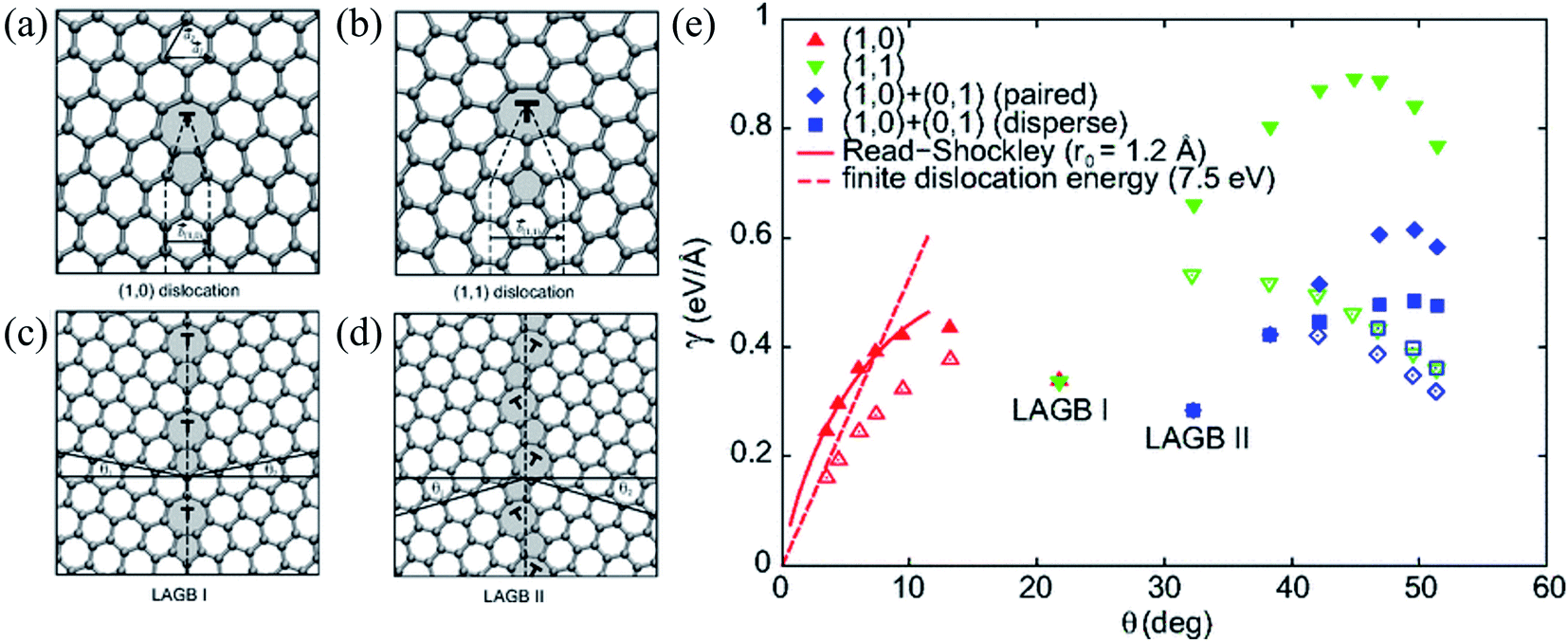 | ||
| Fig. 8 (a and b) Atomic structures of (1, 0) and (1, 1) dislocations. The dashed lines delimit the semi-infinite strips of graphene introduced at the dislocation core. Non-hexagonal rings are shaded. (c and d) Atomic structures of the y = 21.81 (LAGB I) and the y = 32.21 (LAGB II) symmetric large-angle grain boundaries, respectively. The dashed lines show the boundary lines and the solid lines definite angles y1 and y2 (y = y1 + y2) defining orientations of the graphene grains. (e) Grain-boundary energy per unit length g as a function of misorientation angle y for various flat (filled symbols) and buckled (open symbols) grain-boundary structures. The two energetically favorable large-angles grain boundaries, LAGB I and LAGB II, are labeled. The dashed curves show the asymptotic linear dependence of g for the buckled small-angle armchair grain boundaries (Ef = 7.5 eV). Reprinted with permission from ref. 299. Copyright 2010 American Physical Society. | ||
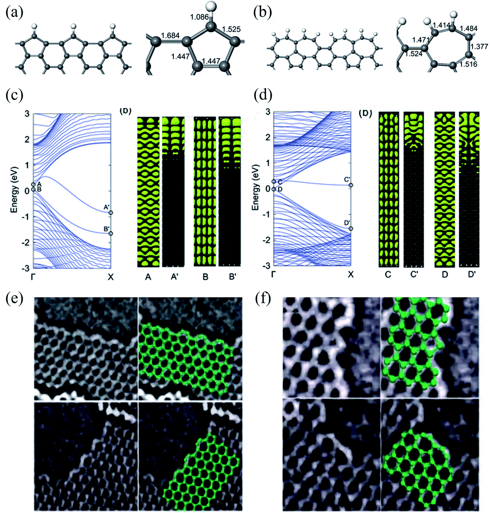 | ||
| Fig. 9 Relaxed geometries of reconstructed armchair graphene edges: (a) pentagonal armchair edge with missing carbon atoms [ac(56)] and (b) reconstructed armchair edge in which two heptagons created by the Stone–Wales transformation share a side [ac(677)]. The bond lengths (in Å) at the graphene edges are shown in the right panel. (c) Band structure of a GNR with an ac(56) edge (left panel), and electronic densities of two edge-related states (right panel). The labels A(B) and A′(B′) indicate electronic densities in the same band at Γ and X, respectively. (d) Band structure of a GNR with the ac(677) edge (left panel), and electronic densities of two edge-related states (right panel). The labels C(D) and C′(D′) indicate electronic densities in the same band at Γ and X, respectively. Reprinted with permission from ref. 329. Copyright 2008 American Physical Society. Experimental evidence of: (e) zigzag edge reconstruction and (f) armchair edge reconstruction. Reprinted with permission from ref. 332. Copyright 2009 American Physical Society. | ||
Therefore, to better understand the edge effects on the band structure of GNRs theoretically, one should either develop more accurate calculations than those for standard ZGNRs and AGNRs20,335 or consider the real structure of the edges.329,332,336 The edge defects in graphene nanoribbons were observed via Raman spectra,337,338 STM,339 and high-resolution electronic transmission microscopy.115,340,341 The edge disorder leads to the conduction gap in the GNRs.342 Li et al.343 reported that the current–voltage characteristic is reduced in vacancy on the edge of ZGNR and induces the conductance gap near the Fermi energy using DFT. The edge disorder leads to the metal–semiconductor transformation in the ZGNR. However, it changes the properties of AGNRs slightly.344 On the other hand, the GNRs are affected by the dephasing process because of thermal environmental fluctuations and electron–electron interaction. As a result, decoherence transport is needed to obtain realistic results.345 The Büttiker probe model346 or self-consistent Born approximation347 can use the dephasing scattering processes in non-equilibrium Green function formalism. It is well known that the surface plasmon resonance frequency in GNRs is a function of the width and the carrier density of the ribbons.348 Although challenging to characterize at the nanoscale, the inactive edge has been evidenced by Raman spectroscopy349 and microwave atomic force microscopy350,351 to show different characteristics than in the basal plane. In addition, Fei et al.352 also reported that the carrier density is enhanced near the sample edge using near-field infrared nanoimaging in exfoliated graphene. The patterned graphene edges have profound effects on doping, scattering, and plasmon reflection, presumably caused by edge defects and roughness353 using the lithographically patterned CVD technique. Edge states introduced on GNRs using lithography constantly change the background charge density.354 Therefore, graphene edges are assumed to be efficient doping centers through the passivation and functionalization of the edges.355 The effect of the vacancy edge defect (bonds breaking between carbon atoms) of a graphene sheet on the Raman spectrum was studied by Ten et al.,356 and they found common changes in the Raman spectrum for the presence of nitrogen and oxygen atoms. A steric effect decreased the stretching vibration q (CH) frequency, which appeared in 2700 cm−1 and corresponded to the 2D vibration. The vacancy edge defect modeling results for the nitrogen-doped graphene sheet fragment functionalized by oxygen atoms were compared with experimental TEM data.113,115
Moreover, Park et al.330 investigated the roles of the pseudospin and the valley degeneracy in electron scattering at graphene edges using experimental techniques such as STM and theoretical analyses. They discovered that charge density modulations of short-wavelength oscillations and gradually decaying beat patterns strongly correlate with pseudospin and valley degeneracy. Furthermore, they claimed that the armchair edge exhibits nearly perfect intervalley scattering with variation in pseudospin. In contrast, the zigzag edge shows intervalley scattering only with the change in pseudospin orientation. They also simulated the armchair edge with pentagons332 and found an atomic-scale node-like structure in the y-axis direction. The zigzag edge, however, was not found to have a periodic modulation like a node.
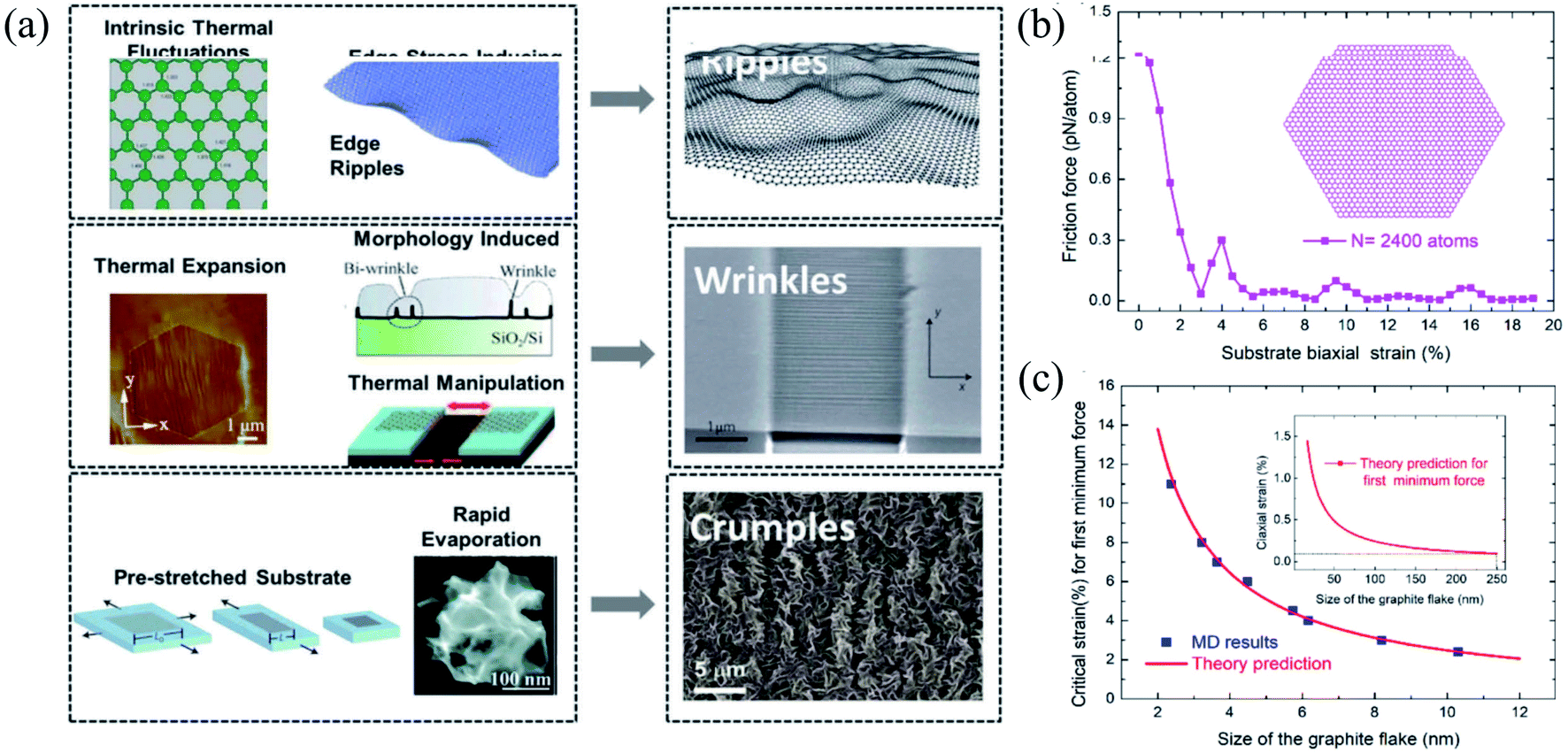 | ||
| Fig. 10 (a) Three types of corrugations: ripples, wrinkles, and crumples. Reprinted with permission from ref. 372. Copyright 2015 they published by Elsevier Ltd. (b and c) Size effects of the flake on friction under different biaxial stretching strains in the substrate: (b) flake containing 2400 atoms and (c) MD simulations versus theories of the critical strain for first minimum friction. Reprinted with permission from ref. 385. Copyright 2019 the American Chemical Society. | ||
As a result, it does not show any piezoelectric behavior; however, several experimental and theoretical studies have shown the modification or engineering of graphene to achieve a piezoelectric response.406 Wang et al.407 reported the in-plain direct piezoelectric effect when in-plain biaxial strain is applied using the AFM tip on graphene membranes across the supported/suspended graphene boundary, and band bending occurs because of biaxial strain. Graphene grown on metallic substrates often shows a periodic superstructure. Periodic height modulations have been measured in suspended graphene samples because of the mismatch between the expansion coefficients of graphene and substrate. Strains in suspended samples can be expected during the fabrication process. Many suspended samples show scrolls that induce significant curvatures and elastic strains.408 Recently, Hsu et al.409 reported an approach to manipulating the topological states by applying strain at room temperature and found an induced giant pseudo-magnetic field (up to ∼800 T) in strained graphene.
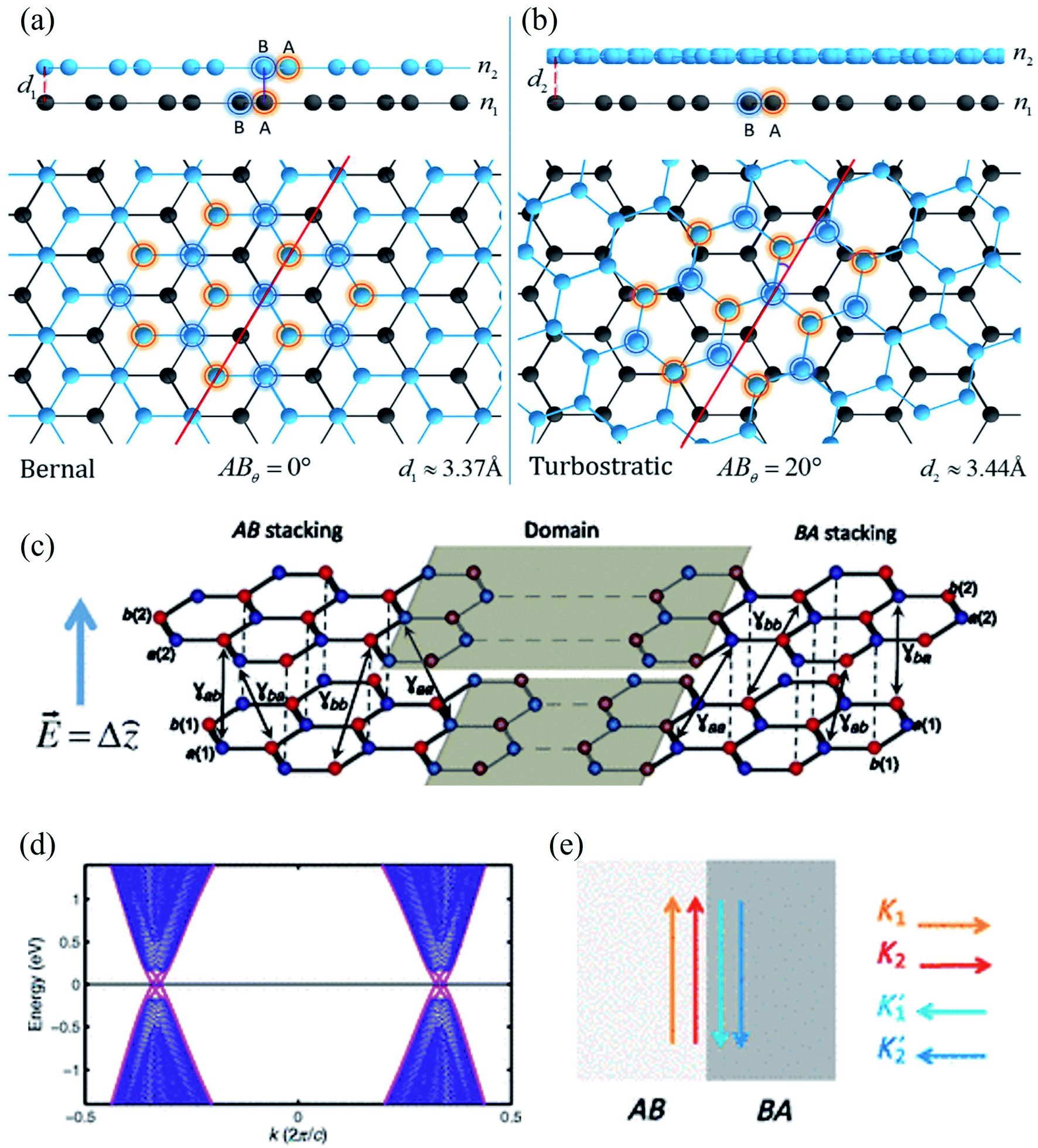 | ||
| Fig. 11 (a) Bernal phase, or AB stacked, BLG and (b) turbostratic-stacked BLG. Reprinted with permission of ref. 424. Copyright 2020 Nature publishing group. (c) A typical AB–BA stacked BLG under strain, (d) the resulting band structure, and (e) schematics of valley-momentum-locked edge states at a tilt boundary. Reprinted with permission from ref. 425. Copyright 2013 the American Physical Society. | ||
Ochapski et al.428 investigated the influence of the defect density in multilayer graphene sheets (prepared via CVD on Ni substrates) on Li intercalation at room temperature using X-ray photoelectron spectroscopy. They found that Li intercalation is independent of the amount of defect induced, and the edges of the graphene flakes are dominant sites for Li adsorption in multilayer graphene. Castro and co-workers429 reported the occurrence of localized states at zigzag edges of N-layer graphene using the tight-binding method. They found the surface states in a single plane in monolayer graphene, finite-amplitude states over the two first or last layers of the stacked bilayer graphene, finite-amplitude states over three consecutive layers, etc. Multilayer graphene edge states were observed because of the next-nearest-neighbor interlayer hopping.
On the other hand, Choi et al.430 investigated monovacancy-induced magnetism in graphene bilayers using DFT methods. Because of the interlayer charge transfer from the adjacent defect-free layer to the vacant layer, spin magnetic moments localized at the vacancy sites of two types of Bernal-stacked graphene bilayers with a monovacancy (B1, B2) decrease by about 10% more than those of a graphene monolayer with a monovacancy. The relaxed structures, spin density plots, band structures, and DOSs of the upper layers of B1, B2, and M are shown in Fig. 12. The Bernal-stacked (AB-type) graphene layer with a single vacancy and a graphene monolayer with a single vacancy are shown in Fig. 12a. The spatial localization of spin densities near the vacancy site and their distributions with mirror symmetry with respect to the y-axis are shown in Fig. 12b. Magnetic moments of 1.31 and 0.04 μB were computed for B1, 1.35 and 0.04 μB for B2, and 1.52 μB for M, respectively. The comparison 2 of band structures among B1, B2 and M was shown in Fig. 12c. The DOSs of the upper layer in graphene bilayers with a single vacancy are shown in Fig. 12d. In Fig. 12c and d, the contributions of spin-up and spin-down electrons were represented by red and black for B1 and M and blue and green for B2 and M, respectively. The band structure showed the localized sp2 dangling bond states at an energy of ∼0.5 eV below the Femi level and quasi-localized defect states pinned at the Fermi level.430 The DOSs revealed that the magnetic moments mainly originate from the localized sp2 dangling-bond states and the contributions of quasi-localized defect states are minor for all three systems considered. An experimental technique was presented to directly manipulate dislocations in situ nanoscale using scanning electron microscopy to measure fundamental properties such as line tension, defect interaction, and node formation in free-standing bilayer graphene based on stacking order (AB or AC).431 Moon et al.432 demonstrated a layer-engineered exfoliation technique for observing large-scale graphene (mm size) with selective thickness control and adjusting these exfoliated layers with different metal films via the spalling mechanism. Recently, the twisted or stacked bilayer (or multilayer) graphene has been attracted significant attention from both theoretical and experimental researchers because of its extraordinary optical433–436 and electronic properties.437–443 These studies shed light on understanding defect structures in graphene where the number of layers is greater than or equal to 2. It could be crucial to use graphene in nanodevice and nanoengineering techniques.
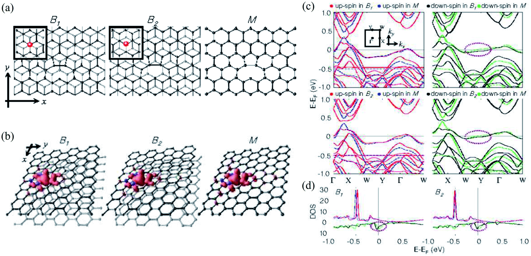 | ||
| Fig. 12 (a) The relaxed structures, (b) spin density plots, (c) band structures and (d) DOS of upper layers of two types of Bernal-stacked graphene bilayers with a single vacancy (B1, B2) and graphene monolayers with a single vacancy (M). Reprinted with permission from ref. 430. Copyright 2008 IOP Publishing Ltd. | ||
3. Summary and outlook
Most of the research on graphene is circumvented around its pristine form. However, inevitable structural defects during the production process affect mechanical, thermal, and electrical properties of graphene and graphene-based nanocomposites. It is hypothetical to obtain a pristine form of graphene because of the method of production, chemical and heat treatment, and electron and ion beam irradiation. Investigating the effect of these defects on graphene's mechanical, thermal, and electrical properties is crucial for fundamental research in nanodevices. For these reasons, researchers shifted their focus to exploring the effect of defects on graphene's mechanical and fracture properties. In addition, charge or spin imbalances between the sublattices of graphene because of its symmetry and zero bandgap characteristics can be created by its interaction with the substrate, which alters its electronic and magnetic properties caused by its modified lattice. Therefore, controlling its interactions with the substrate and the surrounding environment is not easy. Structural modification of the edges, such as bond reconstruction, edge functionalization, passivation, doping, and strain, also tailors the inherent properties of graphene. Moreover, the current focus of the field is on controlling the annealing processes to make defect-free graphene nanostructures. However, a subsequent stage will likely be to create single defects within perfect graphene deliberately (e.g., a small pore, a single step in a zigzag edge, or replacing a single C atom with a Pt atom) with the same level of perfection, which may have several applications, from electronic devices to catalysis.Many fabrication methods for graphene have emerged. However, various kinds of defects, such as vacancies, substitutional impurities, adatoms, and topological defects, are inevitably formed during the growth of graphene because of the imperfection of the graphene production processes. In addition, defects can also be intentionally incorporated into graphene by ion-beam irradiation or chemical treatments. Although the defects in graphene can be helpful in some applications, such as enhancing chemical reactivity and generating magnetism, the defects in graphene can adversely affect thermal conductivity and reduce mechanical strength. Besides, the decrease in the transport properties of graphene has also been attributed to defects. As a result, the large-scale preparation of graphene films with minimal defects has been challenging for commercial applications.
Regarding divacancy's effect on graphene's thermal transport, only the 5–8–5 (two pentagons and one octagon) divacancy was studied. 10% of divacancy defects were reported to reduce the thermal conductivity of graphene by 80%, and the decrease in thermal conductivity of the zigzag graphene nanoribbon is more significant than that of the armchair type for high defect concentration. However, experimental results show that 5–8–5, 555–777 (three pentagons and three heptagons), and 5555–6–7777 (four pentagons, four heptagons, and one hexagon) divacancies are stable and familiar in graphene, and they can propagate in the structure or transform each other. Therefore, it is necessary to systematically study the effect of divacancies with different structures on the thermal transport properties of graphene. In addition, it was found that thermal conductance could be effectively regulated by controlling the orientation or changing the length of the embedded long chain. The decrease in thermal conductance is caused by the change in phonon dispersion and the scattering of defects. However, the influence of 48 extended line defects on the thermal transport properties of the zigzag graphene nanoribbon has not been reported. If we consider the general relevance of divacancies to charge transport in nanotubes, as well as the fact that the 555–777 structure is more stable in graphene than the 5–8–5, it is fascinating to know the answer to questions such as (i) is the 555–777 defect also the most stable configuration in nanotubes? (ii) If not, why is this so, and for what single-walled nanotube diameter will the crossover occur as graphene can be considered infinite diameter tubes? (iii) How does the 555–777 divacancy influence its transport properties? In situ annealing studies of such defects in a dedicated environmental chamber under high-resolution conditions would be rewarding to study the effects of each symmetry-breaking mechanism. Combining tip-enhanced Raman and TEM studies on the same graphene defect could provide unique information about the dynamics of such defects and the changes in the different vibrational modes. A feasibility study using such defects is currently being carried out. However, it is a big challenge to make such defects. The possibility of tailoring the electronic properties of graphene using such defects has been investigated, although control over the precise location remains a challenge. Carbon adatoms can catalyze the formation and dissociation of bonds in graphene because of their under-coordination for bulk sp2 carbon atoms. Still, their exact role and observation of common compound defects in graphene remain unclear.
Most theoretical calculations based on first-principles DFT are limited to a few hundred atoms. At the same time, the accuracy and reliability of the calculation results are questionable when using empirical classical interatomic potentials with many atoms. Therefore, it would be desirable to have a fast computational tool to calculate systems with complex defects and thousands of atoms. In this regard, tight-binding methods can bridge the gap between the first-principles DFT calculations and the simulations using empirical classical potentials. Moreover, the properties of the adatoms adsorbed on the graphene system are strongly dependent on the adsorption configuration (e.g., isolated adatoms versus clusters), so it is crucial not only to understand these effects (configuration-dependent properties and migration) from a theoretical point of view but also to be able to probe them experimentally.
The doping of graphene with transition metals and their spintronics applications is underway. Thus, the study of magnetic substitutional impurities is essential for a theoretical understanding of magnetism for atomic defects in graphene and for explaining experiments in progress that dope graphene with elements of the traditional magnetic bulks (Fe, Co, and Ni). Besides, the origin of electrocatalytic activity and the nature of the electrochemical reaction processes on the M–Nx–G catalysts should be understood to open a new era for the design of graphene-based materials with superior catalytic activity toward electrochemical reactions. Such types of studies would motivate further research in this direction.
The line defect corresponding to grain boundaries in graphene should be paramount. It is well-known that the properties of polycrystalline materials are often dominated by the size of their grains and the atomic structure of the grain boundaries. Still, the role of such systems should be pronounced in graphene, where even a line defect can divide and disrupt a crystal. A more generalized means of forming various types of extended line defects (ELDs), for example, using foreign elements (doped ELDs), is quite demanding. Grain boundaries may govern the transport in such samples. The edges of graphene nanoribbons (GNRs) play a crucial role in modulating their electronic properties. Structural modification of the edges, such as bond reconstruction, edge functionalization, passivation, doping, and strain, leads to alteration of the π-network at the edges. These structural modifications are potential methods to tailor the geometries, stability, electronic properties, spin polarization, spin gap asymmetry, and size of the graphene bandgap. Maximizing the ultimate strength of defected graphene is necessary to optimize it into a versatile energy material. Therefore, a fundamental understanding of such defects' electronic and mechanical properties is essential. The linear defects corresponding to grain boundaries in graphene should be of prime importance because grain boundaries may govern the electronic transport in such samples because of their crucial role in 2D materials. Moreover, the characterization and understanding of the edge atomic structure and termination in graphene and multilayer graphene sheets are vital to future tailoring of the electronic and spin dynamics through controlled edge terminations. Information regarding the system of the intrinsic edges of graphene and multilayer graphene sheets produced via exfoliation is relatively unknown, and further work is needed to build an understanding.
Experimental measurements of the magnetic moment of defective graphene and traces of room temperature ferromagnetism are still limited. These difficulties in observing ferromagnetism in graphene and graphene-based systems are poorly understood and remain debatable. In such conditions, theoretical studies predicting the defective graphene's magnetism using first-principles calculations are appreciable. Unfortunately, graphene's lack of intrinsic magnetism rules out its use for the spin-polarized current generation. One could use ferromagnetic electrodes as intermediates for spin injection, but the efficiency of such a setup is inadequate because of important contact-induced spin relaxation phenomena. Indeed, while AGNRs do not display magnetic ordering, edge-localized magnetic states have been predicted in ZGNRs. However, as these localized states are sensitive to edge roughness, their experimental observation has remained a real challenge for a long time. Although the formation energy of SW defects and the activation energy of SW transformations are reduced by several electron volts at the critical strain, such transformations are still kinetically limited. More significant strains should be applied to observe them experimentally. To heal vacancy defects in graphene in a controlled way would be appreciable. High-temperature thermal annealing, adding foreign atoms, or drawing support from some metal substrates can efficiently remove unwanted defects. However, it is still difficult to regulate the concentration of the defects in the actual experiments, especially for the large area of graphene or batch processing. Therefore, the nature of the healing mechanism should be explored.
Graphene and its derivatives have been used as a substrate for stem cells in regenerative medicine. To use stem cells in transplantation and tissue engineering, it is necessary to stimulate them properly and provide suitable synthetic or natural growth conditions. An additional benefit would be a scaffold material with a controllable and interactive interface with the living cells. Since carbon is an abundant and cheap element, its use for industrial applications would become a part of global sustainability planning by achieving it from CO2 or waste CH4. As a result of their spectacular electronic, thermal, mechanical, and magnetic properties, graphene sheets are expected to offer an exceptional choice in electrochemical energy conversion and storage applications. However, fully realizing their applications in nanoelectronics, sensors, transparent electrodes, energy storage, conversion devices, and biomedicine still requires much fundamental research for the controlled introduction of intrinsic and extrinsic defects in the growth process in the future. This review is expected to understand the vital role of structural defects in graphene and consequently help investigate graphene defects for potential applications.
Conflicts of interest
The authors declare no competing financial interest.Acknowledgements
Basic Science Research Program supported this work through the National Research Foundation of Korea funded by the Ministry of Education (NRF-2020R1A6A1A03043435).References
- H. W. Kroto, J. R. Heath, S. C. O'Brien, R. F. Curl and R. E. Smalley, Nature, 1985, 318, 162–163 CrossRef CAS.
- S. Iijima, Nature, 1991, 354, 56–58 CrossRef CAS.
- K. S. Novoselov, A. K. Geim, S. V. Morozov, D.-e. Jiang, Y. Zhang, S. V. Dubonos, I. V. Grigorieva and A. A. Firsov, Science, 2004, 306, 666–669 CrossRef CAS PubMed.
- P. R. Wallace, Phys. Rev., 1947, 71, 622 CrossRef CAS.
- A. K. Geim, Phys. Scr., 2012, 2012, 014003 CrossRef.
- H.-P. Boehm, A. Clauss, G. Fischer and U. Hofmann, Z. Anorg. Allg. Chem., 1962, 316, 119–127 CrossRef CAS.
- R. Pearce, T. Iakimov, M. Andersson, L. Hultman, A. L. Spetz and R. Yakimova, Sens. Actuators, B, 2011, 155, 451–455 CrossRef CAS.
- T. Kuila, S. Bose, P. Khanra, A. K. Mishra, N. H. Kim and J. H. Lee, Biosens. Bioelectron., 2011, 26, 4637–4648 CrossRef CAS PubMed.
- G. Singh, A. Choudhary, D. Haranath, A. G. Joshi, N. Singh, S. Singh and R. Pasricha, Carbon, 2012, 50, 385–394 CrossRef CAS.
- F. Chen, J. Xia, D. K. Ferry and N. Tao, Nano Lett., 2009, 9, 2571–2574 CrossRef CAS PubMed.
- L.-F. Mao, Nanotechnology, 2009, 20, 275203 CrossRef PubMed.
- E. W. Hill, A. K. Geim, K. Novoselov, F. Schedin and P. Blake, IEEE Trans. Magn., 2006, 42, 2694–2696 Search PubMed.
- M. Kaukonen, A. Krasheninnikov, E. Kauppinen and R. Nieminen, ACS Catal., 2013, 3, 159–165 CrossRef CAS.
- Z. Qin, Z. Li, M. Zhang, B. Yang and R. Outlaw, J. Power Sources, 2012, 217, 303–308 CrossRef CAS.
- G. Wang, B. Wang, X. Wang, J. Park, S. Dou, H. Ahn and K. Kim, J. Mater. Chem., 2009, 19, 8378–8384 RSC.
- M. Pumera, Energy Environ. Sci., 2011, 4, 668–674 RSC.
- Y. Niimi, T. Matsui, H. Kambara, K. Tagami, M. Tsukada and H. Fukuyama, Appl. Surf. Sci., 2005, 241, 43–48 CrossRef CAS.
- Y. Kobayashi, K.-i. Fukui, T. Enoki, K. Kusakabe and Y. Kaburagi, Phys. Rev. B: Condens. Matter Mater. Phys., 2005, 71, 193406 CrossRef.
- D. Klein, Chem. Phys. Lett., 1994, 217, 261–265 CrossRef.
- M. Fujita, K. Wakabayashi, K. Nakada and K. Kusakabe, J. Phys. Soc. Jpn., 1996, 65, 1920–1923 CrossRef CAS.
- R. Saito, M. Fujita, G. Dresselhaus and u. M. Dresselhaus, Appl. Phys. Lett., 1992, 60, 2204–2206 CrossRef CAS.
- Y.-W. Son, M. L. Cohen and S. G. Louie, Phys. Rev. Lett., 2006, 97, 216803 CrossRef PubMed.
- L. Tapasztó, G. Dobrik, P. Lambin and L. P. Biro, Nat. Nanotechnol., 2008, 3, 397–401 CrossRef PubMed.
- S. S. Datta, D. R. Strachan, S. M. Khamis and A. C. Johnson, Nano Lett., 2008, 8, 1912–1915 CrossRef CAS PubMed.
- C. Berger, Z. Song, X. Li, X. Wu, N. Brown, C. Naud, D. Mayou, T. Li, J. Hass and A. N. Marchenkov, Science, 2006, 312, 1191–1196 CrossRef CAS PubMed.
- F. Banhart, J. Kotakoski and A. V. Krasheninnikov, ACS Nano, 2011, 5, 26–41 CrossRef CAS PubMed.
- M. Maruyama, K. Kusakabe, S. Tsuneyuki, K. Akagi, Y. Yoshimoto and J. Yamauchi, J. Phys. Chem. Solids, 2004, 65, 119–122 CrossRef CAS.
- D. Gunlycke, J. Li, J. Mintmire and C. White, Appl. Phys. Lett., 2007, 91, 112108 CrossRef.
- O. Hod, V. Barone, J. E. Peralta and G. E. Scuseria, Nano Lett., 2007, 7, 2295–2299 CrossRef CAS PubMed.
- N. Gorjizadeh, A. A. Farajian, K. Esfarjani and Y. Kawazoe, Phys. Rev. B: Condens. Matter Mater. Phys., 2008, 78, 155427 CrossRef.
- Q. Tang, Z. Zhou and Z. Chen, Nanoscale, 2013, 5, 4541–4583 RSC.
- M. N. Groves, C. Malardier-Jugroot and M. Jugroot, J. Phys. Chem. C, 2012, 116, 10548–10556 CrossRef CAS.
- M. Groves, A. Chan, C. Malardier-Jugroot and M. Jugroot, Chem. Phys. Lett., 2009, 481, 214–219 CrossRef CAS.
- H. Liu, Y. Liu and D. Zhu, J. Mater. Chem., 2011, 21, 3335–3345 RSC.
- Y.-H. Lu, M. Zhou, C. Zhang and Y.-P. Feng, J. Phys. Chem. C, 2009, 113, 20156–20160 CrossRef CAS.
- E. Song, Z. Wen and Q. Jiang, J. Phys. Chem. C, 2011, 115, 3678–3683 CrossRef CAS.
- Q. Jiang, Z. Ao, S. Li and Z. Wen, RSC Adv., 2014, 4, 20290–20296 RSC.
- Y. Tang, Z. Yang and X. Dai, Phys. Chem. Chem. Phys., 2012, 14, 16566–16572 RSC.
- T. Hongwei, F. Wei, W. Rui, L. Huiling and H. Xuri, Mol. Phys., 2015, 113, 3514–3523 CrossRef.
- Y. Tang, Z. Yang and X. Dai, J. Chem. Phys., 2011, 135, 224704 CrossRef PubMed.
- T. Alonso-Lanza, A. Ayuela and F. Aguilera-Granja, Phys. Chem. Chem. Phys., 2016, 18, 21913–21920 RSC.
- A. Ambrosi, S. Y. Chee, B. Khezri, R. D. Webster, Z. Sofer and M. Pumera, Angew. Chem., Int. Ed., 2012, 51, 500–503 CrossRef CAS PubMed.
- M. D. Bhatt, G. Lee and J. S. Lee, J. Phys. Chem. C, 2016, 120, 26435–26441 CrossRef CAS.
- W. Orellana, J. Phys. Chem. C, 2013, 117, 9812–9818 CrossRef CAS.
- S. Gao, X. Wei, H. Liu, K. Geng, H. Wang, H. Moehwald and D. Shchukin, J. Mater. Chem. A, 2015, 3, 23376–23384 RSC.
- Z. Lu, G. Xu, C. He, T. Wang, L. Yang, Z. Yang and D. Ma, Carbon, 2015, 84, 500–508 CrossRef CAS.
- A. Nazari, R. Faez and H. Shamloo, Superlattices Microstruct., 2015, 86, 483–492 CrossRef CAS.
- A. W. Robertson, B. Montanari, K. He, C. S. Allen, Y. A. Wu, N. M. Harrison, A. I. Kirkland and J. H. Warner, ACS Nano, 2013, 7, 4495–4502 CrossRef CAS PubMed.
- O. V. Yazyev and L. Helm, Phys. Rev. B: Condens. Matter Mater. Phys., 2007, 75, 125408 CrossRef.
- L. Rodrigo, P. Pou and R. Pérez, Carbon, 2016, 103, 200–208 CrossRef CAS.
- Y. Ma, P. Lehtinen, A. S. Foster and R. M. Nieminen, New J. Phys., 2004, 6, 68 CrossRef.
- F. Gao and S. Gao, Sci. Rep., 2019, 9, 1–5 CrossRef CAS PubMed.
- I. A. Pašti, A. Jovanović, A. S. Dobrota, S. V. Mentus, B. Johansson and N. V. Skorodumova, Phys. Chem. Chem. Phys., 2018, 20, 858–865 RSC.
- A. Tapia, R. Peón-Escalante, C. Villanueva and F. Avilés, Comput. Mater. Sci., 2012, 55, 255–262 CrossRef CAS.
- A. Fedorov, Z. Popov, D. Fedorov, N. Eliseeva, M. Serjantova and A. Kuzubov, Phys. Status Solidi B, 2012, 249, 2549–2552 CrossRef CAS.
- L. Liu, M. Qing, Y. Wang and S. Chen, J. Mater. Sci. Technol., 2015, 31, 599–606 CrossRef CAS.
- G.-D. Lee, C. Wang, E. Yoon, N.-M. Hwang, D.-Y. Kim and K. Ho, Phys. Rev. Lett., 2005, 95, 205501 CrossRef PubMed.
- J. Kotakoski, A. Krasheninnikov, U. Kaiser and J. Meyer, Phys. Rev. Lett., 2011, 106, 105505 CrossRef CAS PubMed.
- S. T. Skowron, I. V. Lebedeva, A. M. Popov and E. Bichoutskaia, Chem. Soc. Rev., 2015, 44, 3143–3176 RSC.
- W. Zhang, W.-C. Lu, H.-X. Zhang, K. Ho and C. Wang, Carbon, 2016, 110, 330–335 CrossRef CAS.
- L. Wu, T. Hou, Y. Li, K. Chan and S.-T. Lee, J. Phys. Chem. C, 2013, 117, 17066–17072 CrossRef CAS.
- S. N. Shirodkar and U. V. Waghmare, Phys. Rev. B: Condens. Matter Mater. Phys., 2012, 86, 165401 CrossRef.
- J. Ma, D. Alfè, A. Michaelides and E. Wang, Phys. Rev. B: Condens. Matter Mater. Phys., 2009, 80, 033407 CrossRef.
- L. Li, S. Reich and J. Robertson, Phys. Rev. B: Condens. Matter Mater. Phys., 2005, 72, 184109 CrossRef.
- X. Dai, J. Zhao, M. Xie, Y. Tang, Y. Li and B. Zhao, Eur. Phys. J. B, 2011, 80, 343–349 CrossRef CAS.
- R. Dettori, E. Cadelano and L. Colombo, J. Phys.: Condens. Matter, 2012, 24, 104020 CrossRef PubMed.
- H. Yin, X. Shi, C. He, M. Martinez-Canales, J. Li, C. J. Pickard, C. Tang, T. Ouyang, C. Zhang and J. Zhong, Phys. Rev. B, 2019, 99, 041405 CrossRef CAS.
- D. J. Appelhans, Z. Lin and M. T. Lusk, Phys. Rev. B: Condens. Matter Mater. Phys., 2010, 82, 073410 CrossRef.
- J. Lahiri, Y. Lin, P. Bozkurt, I. I. Oleynik and M. Batzill, Nat. Nanotechnol., 2010, 5, 326–329 CrossRef CAS PubMed.
- O. V. Yazyev, Rep. Prog. Phys., 2010, 73, 056501 CrossRef.
- R. Ansari, S. Ajori and B. Motevalli, Superlattices Microstruct., 2012, 51, 274–289 CrossRef CAS.
- A. Zandiatashbar, G.-H. Lee, S. J. An, S. Lee, N. Mathew, M. Terrones, T. Hayashi, C. R. Picu, J. Hone and N. Koratkar, Nat. Commun., 2014, 5, 1–9 Search PubMed.
- G. López-Polín, C. Gómez-Navarro, V. Parente, F. Guinea, M. I. Katsnelson, F. Perez-Murano and J. Gómez-Herrero, Nat. Phys., 2015, 11, 26–31 Search PubMed.
- Y. Li, Z. Zhou, G. Yu, W. Chen and Z. Chen, J. Phys. Chem. C, 2010, 114, 6250–6254 CrossRef CAS.
- Y. Kim, J. Ihm, E. Yoon and G.-D. Lee, Phys. Rev. B: Condens. Matter Mater. Phys., 2011, 84, 075445 CrossRef.
- Q.-K. Li, X.-F. Li, G. Zhang and J. Jiang, J. Am. Chem. Soc., 2018, 140, 15149–15152 CrossRef CAS PubMed.
- M. Lalitha, S. S. Mahadevan and S. Lakshmipathi, J. Mater. Sci., 2017, 52, 815–831 CrossRef CAS.
- Y. Tang, Z. Yang, X. Dai, D. Ma and Z. Fu, J. Phys. Chem. C, 2013, 117, 5258–5268 CrossRef CAS.
- F. Li, J. Zhao and Z. Chen, J. Phys. Chem. C, 2012, 116, 2507–2514 CrossRef CAS.
- H.-p. Zhang, X.-g. Luo, H.-t. Song, X.-y. Lin, X. Lu and Y. Tang, Appl. Surf. Sci., 2014, 317, 511–516 CrossRef CAS.
- P. Wu, P. Du, H. Zhang and C. Cai, Phys. Chem. Chem. Phys., 2015, 17, 1441–1449 RSC.
- Y. Tang, W. Chen, Z. Shen, C. Li, D. Ma and X. Dai, Phys. Chem. Chem. Phys., 2018, 20, 2284–2295 RSC.
- M. Saito, K. Yamashita and T. Oda, Jpn. J. Appl. Phys., 2007, 46, L1185 CrossRef CAS.
- A. El-Barbary, R. Telling, C. Ewels, M. Heggie and P. Briddon, Phys. Rev. B: Condens. Matter Mater. Phys., 2003, 68, 144107 CrossRef.
- P. O. Lehtinen, A. S. Foster, Y. Ma, A. Krasheninnikov and R. M. Nieminen, Phys. Rev. Lett., 2004, 93, 187202 CrossRef CAS PubMed.
- J. M. Carlsson and M. Scheffler, Phys. Rev. Lett., 2006, 96, 046806 CrossRef PubMed.
- R. G. Amorim, A. Fazzio, A. Antonelli, F. D. Novaes and A. J. da Silva, Nano Lett., 2007, 7, 2459–2462 CrossRef CAS PubMed.
- M. M. Ugeda, I. Brihuega, F. Guinea and J. M. Gómez-Rodríguez, Phys. Rev. Lett., 2010, 104, 096804 CrossRef CAS PubMed.
- J. Palacios and F. Ynduráin, Phys. Rev. B: Condens. Matter Mater. Phys., 2012, 85, 245443 CrossRef.
- H. Padmanabhan and B. Nanda, Phys. Rev. B, 2016, 93, 165403 CrossRef.
- Y. Zhang, F. Gao, S. Gao and L. He, Sci. Bull., 2020, 65, 194–200 CrossRef CAS.
- M. G. Menezes and R. B. Capaz, J. Phys.: Condens. Matter, 2015, 27, 335302 CrossRef PubMed.
- Y. Zhou, A. Lii-Rosales, M. Kim, M. Wallingford, D. Jing, M. C. Tringides, C.-Z. Wang and P. A. Thiel, Carbon, 2018, 127, 305–311 CrossRef CAS.
- M. Buettner, P. Choudhury, J. K. Johnson and J. T. Yates Jr, Carbon, 2011, 49, 3937–3952 CrossRef CAS.
- T. Hu, D. Ma, Q. Fang, P. Zhang, X. Liu, R. Wei, Y. Pan, K. Xu and F. Ma, Carbon, 2019, 146, 313–319 CrossRef CAS.
- Z. Yang, S. Bhowmick, F. G. Sen, A. Banerji and A. T. Alpas, Sci. Rep., 2018, 8, 1–13 Search PubMed.
- X.-L. Ye, J. Cai, X.-D. Yang, X.-Y. Tang, Z.-Y. Zhou, Y.-Z. Tan, S.-Y. Xie and L.-S. Zheng, J. Mater. Chem. A, 2017, 5, 24257–24262 RSC.
- P. A. Denis and F. Iribarne, J. Phys. Chem. C, 2013, 117, 19048–19055 CrossRef CAS.
- X. Peng and R. Ahuja, Nano Lett., 2008, 8, 4464–4468 CrossRef CAS PubMed.
- M. G. Menezes, R. B. Capaz and J. L. Faria, Phys. Rev. B: Condens. Matter Mater. Phys., 2010, 82, 245414 CrossRef.
- Y. Orimoto, K. Otsuka, K. Yagyu, H. Tochihara, T. Suzuki and Y. Aoki, J. Phys. Chem. C, 2017, 121, 7294–7302 CrossRef CAS.
- F. Yao, F. Gunes, H. Q. Ta, S. M. Lee, S. J. Chae, K. Y. Sheem, C. S. Cojocaru, S. S. Xie and Y. H. Lee, J. Am. Chem. Soc., 2012, 134, 8646–8654 CrossRef CAS PubMed.
- A. Markevich, R. Jones, S. Öberg, M. Rayson, J. Goss and P. Briddon, Phys. Rev. B: Condens. Matter Mater. Phys., 2012, 86, 045453 CrossRef.
- T. P. Kaloni, M. U. Kahaly, Y. Cheng and U. Schwingenschlögl, J. Mater. Chem., 2012, 22, 23340–23343 RSC.
- J. Coraux, A. T. N ‘Diaye, C. Busse and T. Michely, Nano Lett., 2008, 8, 565–570 CrossRef CAS PubMed.
- J. Červenka, M. Katsnelson and C. Flipse, Nat. Phys., 2009, 5, 840–844 Search PubMed.
- O. V. Yazyev and S. G. Louie, Nat. Mater., 2010, 9, 806–809 CrossRef CAS PubMed.
- B. W. Jeong, J. Ihm and G.-D. Lee, Phys. Rev. B: Condens. Matter Mater. Phys., 2008, 78, 165403 CrossRef.
- L. Kou, C. Tang, W. Guo and C. Chen, ACS Nano, 2011, 5, 1012–1017 CrossRef CAS PubMed.
- X. Lin and J. Ni, Phys. Rev. B: Condens. Matter Mater. Phys., 2011, 84, 075461 CrossRef.
- A. Hashimoto, K. Suenaga, A. Gloter, K. Urita and S. Iijima, Nature, 2004, 430, 870–873 CrossRef CAS PubMed.
- M. H. Gass, U. Bangert, A. L. Bleloch, P. Wang, R. R. Nair and A. Geim, Nat. Nanotechnol., 2008, 3, 676–681 CrossRef CAS PubMed.
- J. C. Meyer, C. Kisielowski, R. Erni, M. D. Rossell, M. Crommie and A. Zettl, Nano Lett., 2008, 8, 3582–3586 CrossRef CAS PubMed.
- J. H. Warner, M. H. Rümmeli, L. Ge, T. Gemming, B. Montanari, N. M. Harrison, B. Büchner and G. A. D. Briggs, Nat. Nanotechnol., 2009, 4, 500–504 CrossRef CAS PubMed.
- Ç. O. Girit, J. C. Meyer, R. Erni, M. D. Rossell, C. Kisielowski, L. Yang, C.-H. Park, M. Crommie, M. L. Cohen and S. G. Louie, Science, 2009, 323, 1705–1708 CrossRef PubMed.
- L. Tapaszto, G. Dobrik, P. Nemes-Incze, G. Vertesy, P. Lambin and L. P. Biro, Phys. Rev. B: Condens. Matter Mater. Phys., 2008, 78, 233407 CrossRef.
- T. Susi, M. Kaukonen, P. Havu, M. P. Ljungberg, P. Ayala and E. I. Kauppinen, Beilstein J. Nanotechnol., 2014, 5, 121–132 CrossRef PubMed.
- L. Openov and A. Podlivaev, Phys. Solid State, 2015, 57, 1477–1481 CrossRef CAS.
- H. F. Bettinger, B. I. Yakobson and G. E. Scuseria, J. Am. Chem. Soc., 2003, 125, 5572–5580 CrossRef CAS PubMed.
- V. H. Crespi, L. X. Benedict, M. L. Cohen and S. G. Louie, Phys. Rev. B: Condens. Matter Mater. Phys., 1996, 53, R13303 CrossRef CAS PubMed.
- M. B. Nardelli, B. I. Yakobson and J. Bernholc, Phys. Rev. B: Condens. Matter Mater. Phys., 1998, 57, R4277 CrossRef.
- C. Ewels, M. Heggie and P. Briddon, Chem. Phys. Lett., 2002, 351, 178–182 CrossRef CAS.
- W.-W. Wang, J.-S. Dang, J.-J. Zheng, X. Zhao, E. Ōsawa and S. Nagase, J. Mater. Chem., 2012, 22, 16370–16375 RSC.
- C. Wang and Y.-h. Ding, J. Mater. Chem. A, 2013, 1, 1885–1891 RSC.
- L. Chen, H. Hu, Y. Ouyang, H. Pan, Y. Sun and F. Liu, Carbon, 2011, 49, 3356–3361 CrossRef CAS.
- L. Chen, J. Li, D. Li, M. Wei and X. Wang, Solid State Commun., 2012, 152, 1985–1989 CrossRef CAS.
- Y. An, A. F. Oliveira, T. Brumme, A. Kuc and T. Heine, Adv. Mater., 2020, 32, 2002442 CrossRef CAS PubMed.
- J. Kumar, Ansh and M. Shrivastava, ACS Omega, 2020, 5, 31281–31288 CrossRef CAS PubMed.
- E. Zaminpayma, M. E. Razavi and P. Nayebi, Appl. Surf. Sci., 2017, 414, 101–106 CrossRef CAS.
- H. Wang, Y. Wang, B. Bai, X. Guo and J. Xue, Appl. Surf. Sci., 2020, 531, 147347 CrossRef CAS.
- X. Long, F. Zhao, H. Liu, J. Huang, Y. Lin, J. Zhu and S. Luo, J. Phys. Chem. C, 2015, 119, 7453–7460 CrossRef CAS.
- S. Ebrahimi and M. Azizi, Mol. Simul., 2018, 44, 236–242 CrossRef CAS.
- D. Boukhvalov and M. Katsnelson, Nano Lett., 2008, 8, 4373–4379 CrossRef CAS PubMed.
- B. Mortazavi and S. Ahzi, Carbon, 2013, 63, 460–470 CrossRef CAS.
- S. Yadav, Z. Zhu and C. V. Singh, Int. J. Hydrogen Energy, 2014, 39, 4981–4995 CrossRef CAS.
- E. J. Duplock, M. Scheffler and P. J. Lindan, Phys. Rev. Lett., 2004, 92, 225502 CrossRef PubMed.
- D. Datta, J. Li, N. Koratkar and V. B. Shenoy, Carbon, 2014, 80, 305–310 CrossRef CAS.
- D. Datta, J. Li and V. B. Shenoy, ACS Appl. Mater. Interfaces, 2014, 6, 1788–1795 CrossRef CAS PubMed.
- Y. Zhang, S.-Y. Li, H. Huang, W.-T. Li, J.-B. Qiao, W.-X. Wang, L.-J. Yin, K.-K. Bai, W. Duan and L. He, Phys. Rev. Lett., 2016, 117, 166801 CrossRef PubMed.
- H. Amara, S. Latil, V. Meunier, P. Lambin and J.-C. Charlier, Phys. Rev. B: Condens. Matter Mater. Phys., 2007, 76, 115423 CrossRef.
- A. Krasheninnikov, P. Lehtinen, A. Foster and R. Nieminen, Chem. Phys. Lett., 2006, 418, 132–136 CrossRef CAS.
- D. Midtvedt and A. Croy, J. Phys.: Condens. Matter, 2016, 28, 045302 CrossRef PubMed.
- M. Sepioni, R. Nair, S. Rablen, J. Narayanan, F. Tuna, R. Winpenny, A. Geim and I. Grigorieva, Phys. Rev. Lett., 2010, 105, 207205 CrossRef CAS PubMed.
- Y. Wang, Y. Huang, Y. Song, X. Zhang, Y. Ma, J. Liang and Y. Chen, Nano Lett, 2009, 9, 220–224 CrossRef CAS PubMed.
- M. Sepioni, R. Nair, I.-L. Tsai, A. Geim and I. Grigorieva, Europhys. Lett., 2012, 97, 47001 CrossRef.
- Z. Yue, D. Seo, K. Ostrikov and X. Wang, Appl. Phys. Lett., 2014, 104, 092417 CrossRef.
- A. M. Valencia and M. J. Caldas, Phys. Rev. B, 2017, 96, 125431 CrossRef.
- S. Y. Kim and H. S. Park, Nanotechnology, 2010, 21, 105710 CrossRef PubMed.
- C. Reddy, S. Rajendran and K. Liew, Int. J. Nanosci., 2005, 4, 631–636 CrossRef CAS.
- M. Wang, C. Yan, L. Ma, N. Hu and M. Chen, Comput. Mater. Sci., 2012, 54, 236–239 CrossRef CAS.
- C. Carpenter, A. Ramasubramaniam and D. Maroudas, Appl. Phys. Lett., 2012, 100, 203105 CrossRef.
- C. Carpenter, D. Maroudas and A. Ramasubramaniam, Appl. Phys. Lett., 2013, 103, 013102 CrossRef.
- X. Sun, Z. Fu, M. Xia and Y. Xu, Theor. App. Mech. Lett., 2014, 4, 051002 CrossRef.
- M. Katsnelson and A. Geim, Philos. Trans. Royal Soc. A, 2008, 366, 195–204 CrossRef CAS PubMed.
- A. J. Stone and D. J. Wales, Chem. Phys. Lett., 1986, 128, 501–503 CrossRef CAS.
- A. Fedorov, D. Fedorov, Z. Popov, Y. E. Anan’eva, N. Eliseeva and A. Kuzubov, J. Exp. Theor. Phys., 2011, 112, 820–824 CrossRef CAS.
- W. Zhang, W.-C. Lu, H.-X. Zhang, K. Ho and C. Wang, J. Phys.: Condens. Matter, 2016, 28, 115001 CrossRef PubMed.
- M. M. Ugeda, I. Brihuega, F. Hiebel, P. Mallet, J.-Y. Veuillen, J. M. Gómez-Rodríguez and F. Ynduráin, Phys. Rev. B: Condens. Matter Mater. Phys., 2012, 85, 121402 CrossRef.
- Z. Hou and K. Terakura, J. Phys. Chem. C, 2015, 119, 4922–4933 CrossRef CAS.
- X. Gao, L. Liu, S. Irle and S. Nagase, Angew. Chem., Int. Ed., 2010, 49, 3200–3202 CrossRef CAS PubMed.
- P. Hirunsit, M. Liangruksa and P. Khanchaitit, Carbon, 2016, 108, 7–20 CrossRef CAS.
- A. Lu and B. Pan, Phys. Rev. Lett., 2004, 92, 105504 CrossRef CAS PubMed.
- J. Kotakoski, A. Krasheninnikov and K. Nordlund, Phys. Rev. B: Condens. Matter Mater. Phys., 2006, 74, 245420 CrossRef.
- L. Liu, J. Gao, X. Zhang, T. Yan and F. Ding, Nanoscale, 2014, 6, 5729–5734 RSC.
- W. S. Paz, W. L. Scopel and J. C. Freitas, Solid State Commun., 2013, 175, 71–75 CrossRef.
- E. Santos, S. Riikonen, D. Sánchez-Portal and A. Ayuela, J. Phys. Chem. C, 2012, 116, 7602–7606 CrossRef CAS.
- O. Cretu, A. V. Krasheninnikov, J. A. Rodríguez-Manzo, L. Sun, R. M. Nieminen and F. Banhart, Phys. Rev. Lett., 2010, 105, 196102 CrossRef PubMed.
- J. Kotakoski, J. C. Meyer, S. Kurasch, D. Santos-Cottin, U. Kaiser and A. V. Krasheninnikov, Phys. Rev. B: Condens. Matter Mater. Phys., 2011, 83, 245420 CrossRef.
- B. Wang, Y. Puzyrev and S. T. Pantelides, Carbon, 2011, 49, 3983–3988 CrossRef CAS.
- J. Kotakoski, D. Santos-Cottin and A. V. Krasheninnikov, ACS Nano, 2012, 6, 671–676 CrossRef CAS PubMed.
- J. Lu, Y. Bao, C. L. Su and K. P. Loh, ACS Nano, 2013, 7, 8350–8357 CrossRef CAS PubMed.
- A. R. Botello-Méndez, X. Declerck, M. Terrones, H. Terrones and J.-C. Charlier, Nanoscale, 2011, 3, 2868–2872 RSC.
- H. Huang, Y. Xu, X. Zou, J. Wu and W. Duan, Phys. Rev. B: Condens. Matter Mater. Phys., 2013, 87, 205415 CrossRef.
- Y. H. Lee, S. G. Kim and D. Tománek, Phys. Rev. Lett., 1997, 78, 2393 CrossRef CAS.
- P. O. Lehtinen, A. S. Foster, A. Ayuela, A. Krasheninnikov, K. Nordlund and R. M. Nieminen, Phys. Rev. Lett., 2003, 91, 017202 CrossRef CAS PubMed.
- L. Tsetseris and S. T. Pantelides, Carbon, 2009, 47, 901–908 CrossRef CAS.
- A. W. Robertson, G.-D. Lee, K. He, E. Yoon, A. I. Kirkland and J. H. Warner, Nano Lett., 2014, 14, 3972–3980 CrossRef CAS PubMed.
- J. C. Meyer, C. O. Girit, M. Crommie and A. Zettl, Nature, 2008, 454, 319–322 CrossRef CAS PubMed.
- G.-D. Lee, A. W. Robertson, S. Lee, Y.-C. Lin, J.-W. Oh, H. Park, Y.-C. Joo, E. Yoon, K. Suenaga and J. H. Warner, Sci. Adv., 2020, 6, eaba4942 CrossRef CAS PubMed.
- C. Ataca, E. Aktürk, H. Şahin and S. Ciraci, J. Appl. Phys., 2011, 109, 013704 CrossRef.
- W.-C. Lu, C. Wang, L.-Z. Zhao, W. Qin and K. Ho, Phys. Rev. B: Condens. Matter Mater. Phys., 2015, 92, 035206 CrossRef.
- R. V. Siriwardane, M.-S. Shen, E. P. Fisher and J. A. Poston, Energy Fuels, 2001, 15, 279–284 CrossRef CAS.
- Z. Chen, S. Deng, H. Wei, B. Wang, J. Huang and G. Yu, Front. Environ. Sci. Eng., 2013, 7, 326–340 CrossRef CAS.
- H. Jüntgen, Fuel, 1986, 65, 1436–1446 CrossRef.
- M. Sevilla and R. Mokaya, Energy Environ. Sci., 2014, 7, 1250–1280 RSC.
- A. D. Roberts, X. Li and H. Zhang, Chem. Soc. Rev., 2014, 43, 4341–4356 RSC.
- F. Banhart, Nanoscale, 2009, 1, 201–213 RSC.
- Y. Gan, L. Sun and F. Banhart, Small, 2008, 4, 587–591 CrossRef CAS PubMed.
- J. A. Rodríguez-Manzo, O. Cretu and F. Banhart, ACS Nano, 2010, 4, 3422–3428 CrossRef PubMed.
- A. Krasheninnikov, P. Lehtinen, A. S. Foster, P. Pyykkö and R. M. Nieminen, Phys. Rev. Lett., 2009, 102, 126807 CrossRef CAS PubMed.
- Y. Mao, J. Yuan and J. Zhong, J. Phys.: Condens. Matter, 2008, 20, 115209 CrossRef PubMed.
- H. Sevinçli, M. Topsakal, E. Durgun and S. Ciraci, Phys. Rev. B: Condens. Matter Mater. Phys., 2008, 77, 195434 CrossRef.
- J. Hu, J. Alicea, R. Wu and M. Franz, Phys. Rev. Lett., 2012, 109, 266801 CrossRef PubMed.
- I. Shtepliuk, N. M. Caffrey, T. Iakimov, V. Khranovskyy, I. A. Abrikosov and R. Yakimova, Sci. Rep., 2017, 7, 1–17 CrossRef CAS PubMed.
- N. Dimakis, F. A. Flor, A. Salgado, K. Adjibi, S. Vargas and J. Saenz, Appl. Surf. Sci., 2017, 421, 252–259 CrossRef CAS.
- H. Salehi, M. Moaddeli and P. Amiri, Surf. Sci., 2016, 647, 96–102 CrossRef CAS.
- Y. Tang, Z. Yang and X. Dai, J. Magn. Magn. Mater., 2011, 323, 2441–2447 CrossRef CAS.
- Z. Guan, S. Ni and S. Hu, ACS Omega, 2020, 5, 5900–5910 CrossRef CAS PubMed.
- N. T. T. Tran, D. K. Nguyen, S. Y. Lin, G. Gumbs and M. F. Lin, ChemPhysChem, 2019, 20, 2473–2481 CrossRef CAS PubMed.
- B. A. Barker, A. J. Bradley, M. M. Ugeda, S. Coh, A. Zettl, M. F. Crommie, S. G. Louie and M. L. Cohen, Phys. Rev. B, 2019, 99, 075431 CrossRef CAS.
- B. P. Paudel, N. Pantha and N. P. Adhikari, Journal of Nepal Physical Society, 2015, 3, 24–34 CrossRef.
- N. Pantha, S. Thapa and N. P. Adhikari, Journal of Institute of Science and Technology, 2020, 25, 15–23 CrossRef.
- L. Liu, Z. Zhou, Q. Guo, Z. Yan, Y. Yao and D. W. Goodman, Surf. Sci., 2011, 605, L47–L50 CrossRef CAS.
- R. Thapa, D. Sen, M. Mitra and K. Chattopadhyay, Phys. B, 2011, 406, 368–373 CrossRef CAS.
- A. Fenta, C. Amorim, J. Gonçalves, N. Fortunato, M. Barbosa, J. Araujo, M. Houssa, S. Cottenier, M. Van Bael and J. Correia, J. Phys.: Mater., 2020, 4, 015002 Search PubMed.
- M. Manadé, F. Viñes and F. Illas, Carbon, 2015, 95, 525–534 CrossRef.
- M. Legesse, F. El Mellouhi, E. T. Bentria, M. E. Madjet, T. S. Fisher, S. Kais and F. H. Alharbi, Appl. Surf. Sci., 2017, 394, 98–107 CrossRef CAS.
- N. Yang, D. Yang, L. Chen, D. Liu, M. Cai and X. Fan, Nanoscale Res. Lett., 2017, 12, 1–7 CrossRef CAS PubMed.
- A. Urich, A. Pospischil, M. M. Furchi, D. Dietze, K. Unterrainer and T. Mueller, Appl. Phys. Lett., 2012, 101, 153113 CrossRef.
- Q. M. Ramasse, R. Zan, U. Bangert, D. W. Boukhvalov, Y.-W. Son and K. S. Novoselov, ACS Nano, 2012, 6, 4063–4071 CrossRef CAS PubMed.
- J. Lee, K. S. Novoselov and H. S. Shin, ACS Nano, 2011, 5, 608–612 CrossRef CAS PubMed.
- S. Sarkar, M. L. Moser, X. Tian, X. Zhang, Y. F. Al-Hadeethi and R. C. Haddon, Chem. Mater., 2014, 26, 184–195 CrossRef CAS.
- R. Zan, U. Bangert, Q. Ramasse and K. S. Novoselov, Nano Lett., 2011, 11, 1087–1092 CrossRef CAS PubMed.
- H. Wang, K. Li, Y. Cheng, Q. Wang, Y. Yao, U. Schwingenschlögl, X. Zhang and W. Yang, Nanoscale, 2012, 4, 2920–2925 RSC.
- F. Schedin, E. Lidorikis, A. Lombardo, V. G. Kravets, A. K. Geim, A. N. Grigorenko, K. S. Novoselov and A. C. Ferrari, ACS Nano, 2010, 4, 5617–5626 CrossRef CAS PubMed.
- P. Wang, D. Zhang, L. Zhang and Y. Fang, Chem. Phys. Lett., 2013, 556, 146–150 CrossRef CAS.
- W.-H. Park, M. Jung, J.-S. Moon, S. Hwan Noh, T. Hyeong Kim, M. Ho Joo and K. Ho Park, Appl. Phys. Lett., 2013, 103, 071903 CrossRef.
- H. Kim, I. Song, C. Park, M. Son, M. Hong, Y. Kim, J. S. Kim, H.-J. Shin, J. Baik and H. C. Choi, ACS Nano, 2013, 7, 6575–6582 CrossRef CAS PubMed.
- H.-C. Lin, Y.-Z. Chen, Y.-C. Wang and Y.-L. Chueh, J. Phys. Chem. C, 2015, 119, 6835–6842 CrossRef CAS.
- H. C. Lee, H. Bong, M. S. Yoo, M. Jo and K. Cho, Small, 2018, 14, 1801181 CrossRef PubMed.
- P. Rani and V. Jindal, RSC Adv., 2013, 3, 802–812 RSC.
- C. Wang, K. Schouteden, Q.-H. Wu, Z. Li, J. Jiang and C. Van Haesendonck, Nanotechnology, 2016, 27, 365702 CrossRef PubMed.
- H.-P. Komsa, J. Kotakoski, S. Kurasch, O. Lehtinen, U. Kaiser and A. V. Krasheninnikov, Phys. Rev. Lett., 2012, 109, 035503 CrossRef PubMed.
- Z.-H. Sheng, H.-L. Gao, W.-J. Bao, F.-B. Wang and X.-H. Xia, J. Mater. Chem., 2012, 22, 390–395 RSC.
- S. Wang, L. Zhang, Z. Xia, A. Roy, D. W. Chang, J. B. Baek and L. Dai, Angew. Chem., Int. Ed., 2012, 51, 4209–4212 CrossRef CAS PubMed.
- L. Zhang and Z. Xia, J. Phys. Chem. C, 2011, 115, 11170–11176 CrossRef CAS.
- L. Zhang, J. Niu, L. Dai and Z. Xia, Langmuir, 2012, 28, 7542–7550 CrossRef CAS PubMed.
- S. Yang, L. Zhi, K. Tang, X. Feng, J. Maier and K. Müllen, Adv. Funct. Mater., 2012, 22, 3634–3640 CrossRef CAS.
- I. Y. Jeon, S. Zhang, L. Zhang, H. J. Choi, J. M. Seo, Z. Xia, L. Dai and J. B. Baek, Adv. Mater., 2013, 25, 6138–6145 CrossRef CAS PubMed.
- L. Zhang, J. Niu, M. Li and Z. Xia, J. Phys. Chem. C, 2014, 118, 3545–3553 CrossRef CAS.
- R. A. Sidik, A. B. Anderson, N. P. Subramanian, S. P. Kumaraguru and B. N. Popov, J. Phys. Chem. B, 2006, 110, 1787–1793 CrossRef CAS PubMed.
- E. Vayner and A. B. Anderson, J. Phys. Chem. C, 2007, 111, 9330–9336 CrossRef CAS.
- L. Yu, X. Pan, X. Cao, P. Hu and X. Bao, J. Catal., 2011, 282, 183–190 CrossRef CAS.
- R. Lv, Q. Li, A. R. Botello-Méndez, T. Hayashi, B. Wang, A. Berkdemir, Q. Hao, A. L. Elías, R. Cruz-Silva and H. R. Gutiérrez, Sci. Rep., 2012, 2, 1–8 Search PubMed.
- Y. Yamada, J. Kim, S. Matsuo and S. Sato, Carbon, 2014, 70, 59–74 CrossRef CAS.
- Y. Yamada, H. Tanaka, S. Kubo and S. Sato, Carbon, 2021, 185, 342–367 CrossRef CAS.
- Y. Yamada, H. Yasuda, K. Murota, M. Nakamura, T. Sodesawa and S. Sato, J. Mater. Sci., 2013, 48, 8171–8198 CrossRef CAS.
- R. Chen, H. Li, D. Chu and G. Wang, J. Phys. Chem. C, 2009, 113, 20689–20697 CrossRef CAS.
- K. A. Kurak and A. B. Anderson, J. Phys. Chem. C, 2009, 113, 6730–6734 CrossRef CAS.
- D. Guo, R. Shibuya, C. Akiba, S. Saji, T. Kondo and J. Nakamura, Science, 2016, 351, 361–365 CrossRef CAS PubMed.
- K. Takeyasu, M. Furukawa, Y. Shimoyama, S. K. Singh and J. Nakamura, Angew. Chem., Int. Ed., 2021, 60, 5121–5124 CrossRef CAS PubMed.
- T. Ishii, M. Philavanh, J. Negishi, E. Inukai and J.-i. Ozaki, ACS Catal., 2022, 12, 1288–1297 CrossRef CAS.
- S.-F. Huang, K. Terakura, T. Ozaki, T. Ikeda, M. Boero, M. Oshima, J.-i. Ozaki and S. Miyata, Phys. Rev. B: Condens. Matter Mater. Phys., 2009, 80, 235410 CrossRef.
- L. Zhao, R. He, K. T. Rim, T. Schiros, K. S. Kim, H. Zhou, C. Gutiérrez, S. Chockalingam, C. J. Arguello and L. Pálová, Science, 2011, 333, 999–1003 CrossRef CAS PubMed.
- T. Marangoni, D. Haberer, D. J. Rizzo, R. R. Cloke and F. R. Fischer, Chem.–Eur. J., 2016, 22, 13037–13040 CrossRef CAS PubMed.
- F. Banhart, J.-C. Charlier and P. Ajayan, Phys. Rev. Lett., 2000, 84, 686 CrossRef CAS PubMed.
- M. Ushiro, K. Uno, T. Fujikawa, Y. Sato, K. Tohji, F. Watari, W.-J. Chun, Y. Koike and K. Asakura, Phys. Rev. B: Condens. Matter Mater. Phys., 2006, 73, 144103 CrossRef.
- M. D. Bhatt and G. Kim, Appl. Surf. Sci., 2021, 569, 150999 CrossRef.
- N. Zhou, N. Wang, Z. Wu and L. Li, Catalysts, 2018, 8, 509 CrossRef.
- Y. Yamada, K. Murota, R. Fujita, J. Kim, A. Watanabe, M. Nakamura, S. Sato, K. Hata, P. Ercius and J. Ciston, J. Am. Chem. Soc., 2014, 136, 2232–2235 CrossRef CAS PubMed.
- J. A. Rodriguez-Manzo and F. Banhart, Nano Lett., 2009, 9, 2285–2289 CrossRef CAS PubMed.
- W. Zhou, M. D. Kapetanakis, M. P. Prange, S. T. Pantelides, S. J. Pennycook and J.-C. Idrobo, Phys. Rev. Lett., 2012, 109, 206803 CrossRef PubMed.
- W. Zhou, J. Lee, J. Nanda, S. T. Pantelides, S. J. Pennycook and J.-C. Idrobo, Nat. Nanotechnol., 2012, 7, 161–165 CrossRef CAS PubMed.
- F. Bonaccorso, Z. Sun, T. Hasan and A. Ferrari, Nat. Photonics, 2010, 4, 611–622 CrossRef CAS.
- A. Lopez-Bezanilla, W. Zhou and J.-C. Idrobo, J. Phys. Chem. Lett., 2014, 5, 1711–1718 CrossRef CAS PubMed.
- C.-p. Cheng, H.-f. Hu, Z.-j. Zhang, Q. Liu, Y. Chen and P. Peng, Mod. Phys. Lett. B, 2014, 28, 1450229 CrossRef CAS.
- M. M. Ervasti, Z. Fan, A. Uppstu, A. V. Krasheninnikov and A. Harju, Phys. Rev. B: Condens. Matter Mater. Phys., 2015, 92, 235412 CrossRef.
- E. J. Santos, A. Ayuela and D. Sánchez-Portal, New J. Phys., 2010, 12, 053012 CrossRef.
- J. Maruyama, N. Fukui, M. Kawaguchi and I. Abe, J. Power Sources, 2008, 182, 489–495 CrossRef CAS.
- V. Bambagioni, C. Bianchini, J. Filippi, A. Lavacchi, W. Oberhauser, A. Marchionni, S. Moneti, F. Vizza, R. Psaro and V. Dal Santo, J. Power Sources, 2011, 196, 2519–2529 CrossRef CAS.
- Q. He, X. Yang, R. He, A. Bueno-López, H. Miller, X. Ren, W. Yang and B. E. Koel, J. Power Sources, 2012, 213, 169–179 CrossRef CAS.
- R. Yang, K. Stevens and J. Dahn, J. Electrochem. Soc., 2007, 155, B79 CrossRef.
- Z. Zhang, S. Yang, M. Dou, H. Liu, L. Gu and F. Wang, RSC Adv., 2016, 6, 67049–67056 RSC.
- M. D. Bhatt, G. Lee and J. S. Lee, Electrochim. Acta, 2017, 228, 619–627 CrossRef CAS.
- Y. Li, R. Hu, X. Wan, J. X. Shang, F. H. Wang and J. Shui, Adv. Theory Simul., 2020, 3, 2000054 CrossRef CAS.
- D. Li, Y. Jia, G. Chang, J. Chen, H. Liu, J. Wang, Y. Hu, Y. Xia, D. Yang and X. Yao, Chem, 2018, 4, 2345–2356 CAS.
- N. Zhang, B. Zhou, D. Li, D. Qi, Y. Wu, H. Zheng and B. Yang, Nanomaterials, 2022, 12, 1044 CrossRef CAS PubMed.
- S. Malola, H. Häkkinen and P. Koskinen, Phys. Rev. B: Condens. Matter Mater. Phys., 2010, 81, 165447 CrossRef.
- P. Y. Huang, C. S. Ruiz-Vargas, A. M. Van Der Zande, W. S. Whitney, M. P. Levendorf, J. W. Kevek, S. Garg, J. S. Alden, C. J. Hustedt and Y. Zhu, Nature, 2011, 469, 389–392 CrossRef CAS PubMed.
- S. Chen, Q. Wu, C. Mishra, J. Kang, H. Zhang, K. Cho, W. Cai, A. A. Balandin and R. S. Ruoff, Nat. Mater., 2012, 11, 203–207 CrossRef CAS PubMed.
- Z. G. Fthenakis and D. Tománek, Phys. Rev. B: Condens. Matter Mater. Phys., 2012, 86, 125418 CrossRef.
- F. Hao, D. Fang and Z. Xu, Appl. Phys. Lett., 2011, 99, 041901 CrossRef.
- A. Bagri, S.-P. Kim, R. S. Ruoff and V. B. Shenoy, Nano Lett., 2011, 11, 3917–3921 CrossRef CAS PubMed.
- Y. Lu and J. Guo, Appl. Phys. Lett., 2012, 101, 043112 CrossRef.
- A. Y. Serov, Z.-Y. Ong and E. Pop, Appl. Phys. Lett., 2013, 102, 033104 CrossRef.
- Z. G. Fthenakis, Z. Zhu and D. Tomanek, Phys. Rev. B: Condens. Matter Mater. Phys., 2014, 89, 125421 CrossRef.
- F. Long, P. Yasaei, R. Sanoj, W. Yao, P. Král, A. Salehi-Khojin and R. Shahbazian-Yassar, ACS Appl. Mater. Interfaces, 2016, 8, 18360–18366 CrossRef CAS PubMed.
- R. M. d. Santos, L. E. d. Sousa, D. S. Galvão and L. A. Ribeiro, Sci. Rep., 2020, 10, 1–8 CrossRef PubMed.
- L. Vicarelli, S. J. Heerema, C. Dekker and H. W. Zandbergen, ACS Nano, 2015, 9, 3428–3435 CrossRef CAS PubMed.
- O. V. Yazyev and Y. P. Chen, Nat. Nanotechnol., 2014, 9, 755–767 CrossRef CAS PubMed.
- D. Wei, Y. Liu, Y. Wang, H. Zhang, L. Huang and G. Yu, Nano Lett., 2009, 9, 1752–1758 CrossRef CAS PubMed.
- X. Wang, X. Li, L. Zhang, Y. Yoon, P. K. Weber, H. Wang, J. Guo and H. Dai, Science, 2009, 324, 768–771 CrossRef CAS PubMed.
- H. Wang, T. Maiyalagan and X. Wang, ACS Catal., 2012, 2, 781–794 CrossRef CAS.
- Y. Li, Z. Zhou, P. Shen and Z. Chen, ACS Nano, 2009, 3, 1952–1958 CrossRef CAS PubMed.
- Y. Fujimoto and S. Saito, Phys. Rev. B: Condens. Matter Mater. Phys., 2011, 84, 245446 CrossRef.
- P. Lambin, H. Amara, F. Ducastelle and L. Henrard, Phys. Rev. B: Condens. Matter Mater. Phys., 2012, 86, 045448 CrossRef.
- N. Ansari, F. Nazari and F. Illas, Phys. Chem. Chem. Phys., 2014, 16, 21473–21485 RSC.
- W. Brito, R. Kagimura and R. Miwa, Phys. Rev. B: Condens. Matter Mater. Phys., 2012, 85, 035404 CrossRef.
- D. Berger and C. Ratsch, Phys. Rev. B, 2016, 93, 235441 CrossRef.
- Y. Liu, J. Song, Y. Li, Y. Liu and Q.-f. Sun, Phys. Rev. B: Condens. Matter Mater. Phys., 2013, 87, 195445 CrossRef.
- D. Gunlycke and C. T. White, Phys. Rev. Lett., 2011, 106, 136806 CrossRef CAS PubMed.
- A. Rycerz, J. Tworzydło and C. Beenakker, Nat. Phys., 2007, 3, 172–175 Search PubMed.
- A. Akhmerov and C. Beenakker, Phys. Rev. Lett., 2007, 98, 157003 CrossRef CAS PubMed.
- Y. Zhang, Z. Jiang, J. Small, M. Purewal, Y.-W. Tan, M. Fazlollahi, J. Chudow, J. Jaszczak, H. Stormer and P. Kim, Phys. Rev. Lett., 2006, 96, 136806 CrossRef CAS PubMed.
- Z. Zhu, A. Collaudin, B. Fauqué, W. Kang and K. Behnia, Nat. Phys., 2012, 8, 89–94 Search PubMed.
- W. Yao, D. Xiao and Q. Niu, Phys. Rev. B: Condens. Matter Mater. Phys., 2008, 77, 235406 CrossRef.
- D. Gunlycke, S. Vasudevan and C. T. White, Nano Lett., 2013, 13, 259–263 CrossRef CAS PubMed.
- S. Haldar, R. G. Amorim, B. Sanyal, R. H. Scheicher and A. R. Rocha, RSC Adv., 2016, 6, 6702–6708 RSC.
- O. V. Yazyev and S. G. Louie, Phys. Rev. B: Condens. Matter Mater. Phys., 2010, 81, 195420 CrossRef.
- A. W. Tsen, L. Brown, M. P. Levendorf, F. Ghahari, P. Y. Huang, R. W. Havener, C. S. Ruiz-Vargas, D. A. Muller, P. Kim and J. Park, Science, 2012, 336, 1143–1146 CrossRef CAS PubMed.
- C. Páez, A. Pereira, J. Rodrigues and N. Peres, Phys. Rev. B: Condens. Matter Mater. Phys., 2015, 92, 045426 CrossRef.
- J. Sun, N. Lin, Z. Li, H. Ren, C. Tang and X. Zhao, RSC Adv., 2016, 6, 1090–1097 RSC.
- F. Schedin, A. K. Geim, S. V. Morozov, E. W. Hill, P. Blake, M. I. Katsnelson and K. S. Novoselov, Nat. Mater., 2007, 6, 652–655 CrossRef CAS PubMed.
- H. E. Romero, P. Joshi, A. K. Gupta, H. R. Gutierrez, M. W. Cole, S. A. Tadigadapa and P. C. Eklund, Nanotechnology, 2009, 20, 245501 CrossRef PubMed.
- G. Ko, H.-Y. Kim, J. Ahn, Y.-M. Park, K.-Y. Lee and J. Kim, Current Applied Physics, 2010, 10, 1002–1004 CrossRef.
- C. Chen, S. Hung, M. Yang, C. Yeh, C. Wu, G. Chi, F. Ren and S. Pearton, Appl. Phys. Lett., 2011, 99, 243502 CrossRef.
- H. J. Yoon, J. H. Yang, Z. Zhou, S. S. Yang and M. M.-C. Cheng, Sens. Actuators, B, 2011, 157, 310–313 CrossRef CAS.
- G. T. Feliciano, C. Sanz-Navarro, M. D. Coutinho-Neto, P. Ordejón, R. H. Scheicher and A. R. Rocha, Phys. Rev. Appl., 2015, 3, 034003 CrossRef.
- Y.-H. Zhang, Y.-B. Chen, K.-G. Zhou, C.-H. Liu, J. Zeng, H.-L. Zhang and Y. Peng, Nanotechnology, 2009, 20, 185504 CrossRef PubMed.
- Y.-H. Zhang, L.-F. Han, Y.-H. Xiao, D.-Z. Jia, Z.-H. Guo and F. Li, Comput. Mater. Sci., 2013, 69, 222–228 CrossRef CAS.
- A. R. Rocha, M. Rossi, A. Fazzio and A. J. da Silva, Phys. Rev. Lett., 2008, 100, 176803 CrossRef CAS PubMed.
- A. Rocha, M. Rossi, A. J. da Silva and A. Fazzio, J. Phys. D: Appl. Phys., 2010, 43, 374002 CrossRef.
- R. G. Amorim, A. Fazzio, A. J. da Silva and A. R. Rocha, Nanoscale, 2013, 5, 2798–2803 RSC.
- B. Yang, H. Xu, J. Lu and K. P. Loh, J. Am. Chem. Soc., 2014, 136, 12041–12046 CrossRef CAS PubMed.
- K. Kim, Z. Lee, W. Regan, C. Kisielowski, M. Crommie and A. Zettl, ACS Nano, 2011, 5, 2142–2146 CrossRef CAS PubMed.
- R. Grantab, V. B. Shenoy and R. S. Ruoff, Science, 2010, 330, 946–948 CrossRef CAS PubMed.
- A. Ferreira, X. Xu, C.-L. Tan, S.-K. Bae, N. Peres, B.-H. Hong, B. Özyilmaz and A. C. Neto, Europhys. Lett., 2011, 94, 28003 CrossRef.
- K. S. Novoselov, D. Jiang, F. Schedin, T. Booth, V. Khotkevich, S. Morozov and A. K. Geim, Proc. Natl. Acad. Sci. U. S. A., 2005, 102, 10451–10453 CrossRef CAS PubMed.
- A. C. Neto, F. Guinea, N. M. Peres, K. S. Novoselov and A. K. Geim, Rev. Mod. Phys., 2009, 81, 109 CrossRef.
- N. M. Peres, Rev. Mod. Phys., 2010, 82, 2673 CrossRef CAS.
- D. Bahamon, A. Pereira and P. Schulz, Phys. Rev. B: Condens. Matter Mater. Phys., 2011, 83, 155436 CrossRef.
- L. Jiang, X. Lv and Y. Zheng, Phys. Lett. A, 2011, 376, 136–141 CrossRef CAS.
- Y. You, Z. Ni, T. Yu and Z. Shen, Appl. Phys. Lett., 2008, 93, 163112 CrossRef.
- L. Brey and H. Fertig, Phys. Rev. B: Condens. Matter Mater. Phys., 2006, 73, 235411 CrossRef.
- M. Ezawa, Phys. Rev. B: Condens. Matter Mater. Phys., 2006, 73, 045432 CrossRef.
- M. Acik and Y. J. Chabal, Jpn. J. Appl. Phys., 2011, 50, 070101 CrossRef.
- V. V. Ilyasov, B. Meshi, V. Nguyen, I. V. Ershov and D. Nguyen, J. Appl. Phys., 2014, 115, 053708 CrossRef.
- Y. Li, Z. Zhou, C. R. Cabrera and Z. Chen, Sci. Rep., 2013, 3, 1–6 Search PubMed.
- C. Park, J. Ihm and G. Kim, Phys. Rev. B: Condens. Matter Mater. Phys., 2013, 88, 045403 CrossRef.
- C. Park, H. Yang, A. J. Mayne, G. Dujardin, S. Seo, Y. Kuk, J. Ihm and G. Kim, Proc. Natl. Acad. Sci. U. S. A., 2011, 108, 18622–18625 CrossRef CAS PubMed.
- N. Marzari and D. Vanderbilt, Phys. Rev. B: Condens. Matter Mater. Phys., 1997, 56, 12847 CrossRef CAS.
- P. Koskinen, S. Malola and H. Häkkinen, Phys. Rev. B: Condens. Matter Mater. Phys., 2009, 80, 073401 CrossRef.
- B. Huang, M. Liu, N. Su, J. Wu, W. Duan, B.-l. Gu and F. Liu, Phys. Rev. Lett., 2009, 102, 166404 CrossRef PubMed.
- C. Reddy, A. Ramasubramaniam, V. Shenoy and Y.-W. Zhang, Appl. Phys. Lett., 2009, 94, 101904 CrossRef.
- K. Nakada, M. Fujita, G. Dresselhaus and M. S. Dresselhaus, Phys. Rev. B: Condens. Matter Mater. Phys., 1996, 54, 17954 CrossRef CAS PubMed.
- T. Wassmann, A. P. Seitsonen, A. M. Saitta, M. Lazzeri and F. Mauri, Phys. Rev. Lett., 2008, 101, 096402 CrossRef PubMed.
- L. Cancado, M. Pimenta, B. Neves, M. Dantas and A. Jorio, Phys. Rev. Lett., 2004, 93, 247401 CrossRef CAS PubMed.
- C. Casiraghi, A. Hartschuh, H. Qian, S. Piscanec, C. Georgi, A. Fasoli, K. Novoselov, D. Basko and A. Ferrari, Nano Lett., 2009, 9, 1433–1441 CrossRef CAS PubMed.
- Y. Niimi, T. Matsui, H. Kambara, K. Tagami, M. Tsukada and H. Fukuyama, Phys. Rev. B: Condens. Matter Mater. Phys., 2006, 73, 085421 CrossRef.
- Z. Liu, K. Suenaga, P. J. Harris and S. Iijima, Phys. Rev. Lett., 2009, 102, 015501 CrossRef PubMed.
- X. Jia, M. Hofmann, V. Meunier, B. G. Sumpter, J. Campos-Delgado, J. M. Romo-Herrera, H. Son, Y.-P. Hsieh, A. Reina and J. Kong, Science, 2009, 323, 1701–1705 CrossRef CAS PubMed.
- M. Evaldsson, I. V. Zozoulenko, H. Xu and T. Heinzel, Phys. Rev. B: Condens. Matter Mater. Phys., 2008, 78, 161407 CrossRef.
- J. Li, Z. Li, G. Zhou, Z. Liu, J. Wu, B.-L. Gu, J. Ihm and W. Duan, Phys. Rev. B: Condens. Matter Mater. Phys., 2010, 82, 115410 CrossRef.
- T. Li and S.-P. Lu, Phys. Rev. B: Condens. Matter Mater. Phys., 2008, 77, 085408 CrossRef.
- R. Golizadeh-Mojarad and S. Datta, Phys. Rev. B: Condens. Matter Mater. Phys., 2007, 75, 081301 CrossRef.
- M. Buttiker, IBM J. Res. Dev., 1988, 32, 63–75 Search PubMed.
- G.-Y. Sun and Y.-j. Zhu, J. Electron. Mater., 2013, 42, 1–9 CrossRef CAS.
- L. Ju, B. Geng, J. Horng, C. Girit, M. Martin, Z. Hao, H. A. Bechtel, X. Liang, A. Zettl and Y. R. Shen, Nat. Nanotechnol., 2011, 6, 630–634 CrossRef CAS PubMed.
- D. Bischoff, J. Güttinger, S. Dröscher, T. Ihn, K. Ensslin and C. Stampfer, J. Appl. Phys., 2011, 109, 073710 CrossRef.
- K. Brockdorf, Z. Ji, N. Engel, J. Myers, S. Mou, H. Huang and Y. Zhuang, Mater. Lett., 2018, 211, 183–186 CrossRef CAS.
- Z. Ji, J. Myers, K. Brockdorf, N. Engel, S. Mou, H. Huang and Y. Zhuang, J. Vac. Sci. Technol., 2018, 36, 05G508 CrossRef.
- Z. Fei, A. Rodin, G. O. Andreev, W. Bao, A. McLeod, M. Wagner, L. Zhang, Z. Zhao, M. Thiemens and G. Dominguez, Nature, 2012, 487, 82–85 CrossRef CAS PubMed.
- Z. Fei, M. Goldflam, J.-S. Wu, S. Dai, M. Wagner, A. McLeod, M. Liu, K. Post, S. Zhu and G. Janssen, Nano Lett., 2015, 15, 8271–8276 CrossRef CAS PubMed.
- V. W. Brar, M. S. Jang, M. Sherrott, J. J. Lopez and H. A. Atwater, Nano Lett., 2013, 13, 2541–2547 CrossRef CAS PubMed.
- K. Brenner, Y. Yang and R. Murali, Carbon, 2012, 50, 637–645 CrossRef CAS.
- G. Ten, A. Y. Gerasimenko, M. S. Savelyev, A. V. Kuksin, P. N. Vasilevsky, E. P. Kitsyuk and V. I. Baranov, Letters on Materials, 2020, 10, 89–93 CrossRef.
- Z. Ni, W. Chen, X. Fan, J. Kuo, T. Yu, A. Wee and Z. Shen, Phys. Rev. B: Condens. Matter Mater. Phys., 2008, 77, 115416 CrossRef.
- N. Mermin, Phys. Rev. B: Condens. Matter Mater. Phys., 2006, 74, 149902 CrossRef.
- N. D. Mermin and H. Wagner, Phys. Rev. Lett., 1966, 17, 1133 CrossRef CAS.
- P. Xu, M. Neek-Amal, S. Barber, J. Schoelz, M. Ackerman, P. Thibado, A. Sadeghi and F. Peeters, Nat. Commun., 2014, 5, 1–7 Search PubMed.
- J. Venables, G. Spiller and M. Hanbucken, Rep. Prog. Phys., 1984, 47, 399 CrossRef.
- M. Zinke-Allmang, L. C. Feldman and M. H. Grabow, Surf. Sci. Rep., 1992, 16, 377–463 CrossRef CAS.
- J. Evans, P. Thiel and M. C. Bartelt, Surf. Sci. Rep., 2006, 61, 1–128 CrossRef CAS.
- A. Fasolino, J. Los and M. I. Katsnelson, Nat. Mater., 2007, 6, 858–861 CrossRef CAS PubMed.
- F. Ding, H. Ji, Y. Chen, A. Herklotz, K. Dörr, Y. Mei, A. Rastelli and O. G. Schmidt, Nano Lett., 2010, 10, 3453–3458 CrossRef CAS PubMed.
- H. Pan and B. Chen, Sci. Rep., 2014, 4, 1–8 Search PubMed.
- V. M. Pereira, A. C. Neto and N. Peres, Phys. Rev. B: Condens. Matter Mater. Phys., 2009, 80, 045401 CrossRef.
- H. Pan, Mater. Chem. Phys., 2017, 189, 111–117 CrossRef CAS.
- Q. Zhao, M. B. Nardelli and J. Bernholc, Phys. Rev. B: Condens. Matter Mater. Phys., 2002, 65, 144105 CrossRef.
- P. Jensen, J. Gale and X. Blase, Phys. Rev. B: Condens. Matter Mater. Phys., 2002, 66, 193403 CrossRef.
- Z. Li, P. Dharap, P. Sharma, S. Nagarajaiah and B. I. Yakobson, J. Appl. Phys., 2005, 97, 074303 CrossRef.
- S. Deng and V. Berry, Mater. Today, 2016, 19, 197–212 CrossRef CAS.
- N. Liu, Z. Pan, L. Fu, C. Zhang, B. Dai and Z. Liu, Nano Res., 2011, 4, 996–1004 CrossRef CAS.
- W. Zhu, T. Low, V. Perebeinos, A. A. Bol, Y. Zhu, H. Yan, J. Tersoff and P. Avouris, Nano Lett., 2012, 12, 3431–3436 CrossRef CAS PubMed.
- S. J. Chae, F. Güneş, K. K. Kim, E. S. Kim, G. H. Han, S. M. Kim, H. J. Shin, S. M. Yoon, J. Y. Choi and M. H. Park, Adv. Mater., 2009, 21, 2328–2333 CrossRef CAS.
- J. Zang, S. Ryu, N. Pugno, Q. Wang, Q. Tu, M. J. Buehler and X. Zhao, Nat. Mater., 2013, 12, 321–325 CrossRef CAS PubMed.
- X. Wang, K. Tantiwanichapan, J. W. Christopher, R. Paiella and A. K. Swan, Nano Lett., 2015, 15, 5969–5975 CrossRef CAS PubMed.
- A. L. Kitt, Z. Qi, S. Rémi, H. S. Park, A. K. Swan and B. B. Goldberg, Nano Lett., 2013, 13, 2605–2610 CrossRef CAS PubMed.
- L. Yang, Y. Guo and Q. Zhang, Diamond Relat. Mater., 2017, 73, 273–277 CrossRef CAS.
- Q. Bai, X. He, J. Bai and Z. Tong, AIP Adv., 2016, 6, 055308 CrossRef.
- P. Yin and M. Ma, ACS Appl. Nano Mater., 2018, 1, 6596–6602 CrossRef CAS.
- X. Lin, H. Zhang, Z. Guo and T. Chang, Tribol. Int., 2019, 131, 686–693 CrossRef CAS.
- K. Wang, W. Ouyang, W. Cao, M. Ma and Q. Zheng, Nanoscale, 2019, 11, 2186–2193 RSC.
- Y. Dong, Z. Duan, Y. Tao, Z. Wei, B. Gueye, Y. Zhang and Y. Chen, Tribol. Int., 2019, 136, 259–266 CrossRef CAS.
- K. Wang, C. Qu, J. Wang, W. Ouyang, M. Ma and Q. Zheng, ACS Appl. Mater. Interfaces, 2019, 11, 36169–36176 CrossRef CAS PubMed.
- Z. H. Ni, T. Yu, Y. H. Lu, Y. Y. Wang, Y. P. Feng and Z. X. Shen, ACS Nano, 2008, 2, 2301–2305 CrossRef CAS PubMed.
- G. Gui, J. Li and J. Zhong, Phys. Rev. B: Condens. Matter Mater. Phys., 2008, 78, 075435 CrossRef.
- M. Huang, T. A. Pascal, H. Kim, W. A. Goddard III and J. R. Greer, Nano Lett., 2011, 11, 1241–1246 CrossRef CAS PubMed.
- R. Ribeiro, V. M. Pereira, N. Peres, P. Briddon and A. C. Neto, New J. Phys., 2009, 11, 115002 CrossRef.
- S.-M. Choi, S.-H. Jhi and Y.-W. Son, Phys. Rev. B: Condens. Matter Mater. Phys., 2010, 81, 081407 CrossRef.
- Z. H. Ni, T. Yu, Y. H. Lu, Y. Y. Wang, Y. P. Feng, Z. X. Shen and T. Low, ACS Nano, 2009, 3, 483 CrossRef CAS.
- M. Farjam and H. Rafii-Tabar, Phys. Rev. B: Condens. Matter Mater. Phys., 2009, 80, 167401 CrossRef.
- S. Souma, Y. Ohmi and M. Ogawa, J. Comput. Electron., 2013, 12, 170–174 CrossRef CAS.
- Y. Wei and R. Yang, Natl. Sci. Rev., 2019, 6, 324–348 CrossRef CAS PubMed.
- D. G. Papageorgiou, I. A. Kinloch and R. J. Young, Prog. Mater. Sci., 2017, 90, 75–127 CrossRef CAS.
- Q. Cao, X. Geng, H. Wang, P. Wang, A. Liu, Y. Lan and Q. Peng, Crystals, 2018, 8, 357 CrossRef.
- E. Cadelano, P. L. Palla, S. Giordano and L. Colombo, Phys. Rev. Lett., 2009, 102, 235502 CrossRef PubMed.
- C. Lee, X. Wei, J. W. Kysar and J. Hone, Science, 2008, 321, 385–388 CrossRef CAS PubMed.
- F. Liu, P. Ming and J. Li, Phys. Rev. B: Condens. Matter Mater. Phys., 2007, 76, 064120 CrossRef.
- I. Y. Sagalianov, T. M. Radchenko, Y. I. Prylutskyy, V. A. Tatarenko and P. Szroeder, Eur. Phys. J. B, 2017, 90, 1–9 CrossRef.
- I. Y. Sahalianov, T. Radchenko, V. Tatarenko and Y. I. Prylutskyy, Ann. Phys., 2018, 398, 80–93 CAS.
- T. Radchenko, I. Sahalianov, V. Tatarenko, Y. Prylutskyy, P. Szroeder, M. Kempiński and W. Kempiński, 2018, arXiv:1712.03424.
- T. M. Radchenko, V. A. Tatarenko, V. V. Lizunov, V. B. Molodkin, I. E. Golentus, I. Y. Sahalianov and Y. I. Prylutskyy, Phys. Status Solidi B, 2019, 256, 1800406 CrossRef.
- T. M. Radchenko, I. Y. Sahalianov, V. A. Tatarenko, Y. I. Prylutskyy, P. Szroeder, M. Kempiński and W. Kempiński, Handbook of Graphene Set, 2019, vol. 1, pp. 451–502 Search PubMed.
- I. Y. Sahalianov, T. M. Radchenko, V. A. Tatarenko, G. Cuniberti and Y. I. Prylutskyy, J. Appl. Phys., 2019, 126, 054302 CrossRef.
- A. Mehmood, N. Mubarak, M. Khalid, R. Walvekar, E. Abdullah, M. Siddiqui, H. A. Baloch, S. Nizamuddin and S. Mazari, J. Environ. Chem. Eng., 2020, 8, 103743 CrossRef CAS.
- X. Wang, H. Tian, W. Xie, Y. Shu, W.-T. Mi, M. Ali Mohammad, Q.-Y. Xie, Y. Yang, J.-B. Xu and T.-L. Ren, NPG Asia Mater., 2015, 7, e154 CrossRef CAS.
- F. Guinea, Solid State Commun., 2012, 152, 1437–1441 CrossRef CAS.
- C.-C. Hsu, M. Teague, J.-Q. Wang and N.-C. Yeh, Sci. Adv., 2020, 6, eaat9488 CrossRef CAS PubMed.
- S. Dai, Y. Xiang and D. J. Srolovitz, Nano Lett., 2016, 16, 5923–5927 CrossRef CAS PubMed.
- J. Hicks, M. Sprinkle, K. Shepperd, F. Wang, A. Tejeda, A. Taleb-Ibrahimi, F. Bertran, P. Le Fèvre, W. De Heer and C. Berger, Phys. Rev. B: Condens. Matter Mater. Phys., 2011, 83, 205403 CrossRef.
- E. S. Morell, P. Vargas, L. Chico and L. Brey, Phys. Rev. B: Condens. Matter Mater. Phys., 2011, 84, 195421 CrossRef.
- G. Tarnopolsky, A. J. Kruchkov and A. Vishwanath, Phys. Rev. Lett., 2019, 122, 106405 CrossRef CAS PubMed.
- M. Anđelković, L. Covaci and F. Peeters, Phys. Rev. Mater., 2018, 2, 034004 CrossRef.
- E. J. Mele, Phys. Rev. B: Condens. Matter Mater. Phys., 2010, 81, 161405 CrossRef.
- B.-L. Huang, C.-P. Chuu and M.-F. Lin, Sci. Rep., 2019, 9, 1–12 CrossRef PubMed.
- C.-Y. Lin, J.-Y. Wu, Y.-H. Chiu, C.-P. Chang and M.-F. Lin, Phys. Rev. B: Condens. Matter Mater. Phys., 2014, 90, 205434 CrossRef.
- D. S. Lee, C. Riedl, T. Beringer, A. C. Neto, K. von Klitzing, U. Starke and J. H. Smet, Phys. Rev. Lett., 2011, 107, 216602 CrossRef PubMed.
- C.-C. Lu, Y.-C. Lin, Z. Liu, C.-H. Yeh, K. Suenaga and P.-W. Chiu, ACS Nano, 2013, 7, 2587–2594 CrossRef CAS PubMed.
- W. Yan, W.-Y. He, Z.-D. Chu, M. Liu, L. Meng, R.-F. Dou, Y. Zhang, Z. Liu, J.-C. Nie and L. He, Nat. Commun., 2013, 4, 1–7 Search PubMed.
- J. S. Alden, A. W. Tsen, P. Y. Huang, R. Hovden, L. Brown, J. Park, D. A. Muller and P. L. McEuen, Proc. Natl. Acad. Sci. U. S. A., 2013, 110, 11256–11260 CrossRef CAS PubMed.
- K. Kim, M. Yankowitz, B. Fallahazad, S. Kang, H. C. Movva, S. Huang, S. Larentis, C. M. Corbet, T. Taniguchi and K. Watanabe, Nano Lett., 2016, 16, 1989–1995 CrossRef CAS PubMed.
- L.-J. Yin, H. Jiang, J.-B. Qiao and L. He, Nat. Commun., 2016, 7, 1–6 Search PubMed.
- J. A. Garlow, L. K. Barrett, L. Wu, K. Kisslinger, Y. Zhu and J. F. Pulecio, Sci. Rep., 2016, 6, 1–11 CrossRef PubMed.
- A. Vaezi, Y. Liang, D. H. Ngai, L. Yang and E.-A. Kim, Phys. Rev. X, 2013, 3, 021018 Search PubMed.
- C. Woods, L. Britnell, A. Eckmann, R. Ma, J. Lu, H. Guo, X. Lin, G. Yu, Y. Cao and R. V. Gorbachev, Nat. Phys., 2014, 10, 451–456 Search PubMed.
- C. Gong, S. Lee, S. Hong, E. Yoon, G.-D. Lee and J. H. Warner, Nanoscale, 2017, 9, 13725–13730 RSC.
- M. W. Ochapski, D. Ataç, J. G. Sanderink, A. Y. Kovalgin and M. P. de Jong, Carbon Trends, 2021, 4, 100045 CrossRef.
- E. V. Castro, N. Peres and J. L. dos Santos, Europhys. Lett., 2008, 84, 17001 CrossRef.
- S. Choi, B. W. Jeong, S. Kim and G. Kim, J. Phys.: Condens. Matter, 2008, 20, 235220 CrossRef PubMed.
- Y.-H. Kim, J. Choi, K.-J. Chang and D. Tománek, Phys. Rev. B: Condens. Matter Mater. Phys., 2003, 68, 125420 CrossRef.
- J.-Y. Moon, M. Kim, S.-I. Kim, S. Xu, J.-H. Choi, D. Whang, K. Watanabe, T. Taniguchi, D. S. Park and J. Seo, Sci. Adv., 2020, 6, eabc6601 CrossRef CAS PubMed.
- P. Schweizer, C. Dolle and E. Spiecker, Sci. Adv., 2018, 4, eaat4712 CrossRef CAS PubMed.
- Q. Ye, J. Wang, Z. Liu, Z.-C. Deng, X.-T. Kong, F. Xing, X.-D. Chen, W.-Y. Zhou, C.-P. Zhang and J.-G. Tian, Appl. Phys. Lett., 2013, 102, 021912 CrossRef.
- R. W. Havener, Y. Liang, L. Brown, L. Yang and J. Park, Nano Lett., 2014, 14, 3353–3357 CrossRef CAS PubMed.
- M. De Corato, C. Cocchi, D. Prezzi, M. J. Caldas, E. Molinari and A. Ruini, J. Phys. Chem. C, 2014, 118, 23219–23225 CrossRef CAS.
- S. K. Jain, V. Juričić and G. T. Barkema, 2D Materials, 2016, 4, 015018 CrossRef.
- S. Shallcross, S. Sharma and O. A. Pankratov, Phys. Rev. Lett., 2008, 101, 056803 CrossRef CAS PubMed.
- R. De Gail, M. Goerbig, F. Guinea, G. Montambaux and A. C. Neto, Phys. Rev. B: Condens. Matter Mater. Phys., 2011, 84, 045436 CrossRef.
- R. Bistritzer and A. MacDonald, Phys. Rev. B: Condens. Matter Mater. Phys., 2011, 84, 035440 CrossRef.
- G. Trambly de Laissardière, D. Mayou and L. Magaud, Nano Lett., 2010, 10, 804–808 CrossRef PubMed.
- L. Meng, W. Yan, L. Yin, Z.-D. Chu, Y. Zhang, L. Feng, R. Dou and J. Nie, J. Phys. Chem. C, 2014, 118, 6462–6466 CrossRef CAS.
- K. K. Saha, M. Drndic and B. K. Nikolic, Nano Lett., 2012, 12, 50–55 CrossRef CAS PubMed.
| This journal is © The Royal Society of Chemistry 2022 |