
 Open Access Article
 This Open Access Article is licensed under a Creative Commons Attribution-Non Commercial 3.0 Unported Licence
Luminescence studies in cadmium telluride nanocrystals grown on glass substrates†
Rakhi Grover *a,
Ritu Srivastavab and
Kanchan Saxenaa
*a,
Ritu Srivastavab and
Kanchan Saxenaa
aAmity Institute of Advanced Research and Studies (Materials and Devices) AIARS (M&D) & Amity Institute of Renewable and Alternative Energy AIRAE, Amity University, Sector 125, Noida, UP 201303, India. E-mail: grover.rakhi@gmail.com; rgrover1@amity.edu
bAdvanced Materials and Device Metrology Division, Council of Scientific and Industrial Research-National Physical Laboratory (CSIR-NPL), Dr K. S. Krishnan Road, New Delhi-110012, India
First published on 20th September 2022
Abstract
The thermal evaporation method can easily be employed to fabricate hybrid inorganic-organic LEDs and the emission properties can be controlled by varying the thickness of the nanocrystalline CdTe film. The fabrication of CdTe nanocrystals on glass substrates was demonstrated using a thermal evaporation method. Films were characterised using various experimental tools, such as SEM, TEM, AFM, UV-Vis and PL spectroscopy. The formation of nanoparticles with diameters from 1.5 nm up to 9 nm was observed in the nanocrystalline thin films. The organic light emitting diodes (OLEDs) based on these nanocrystals as an emissive layer exhibit electroluminescence (EL) in the green to yellow region of the visible spectrum, which is ascribed to the varying size dependent EL from the nanocrystals of CdTe present in the thin film. The method demonstrates an easy and convenient way to incorporate inorganic CdTe nanocrystals inside the organic light emitting devices.
1. Introduction
A number of nanomaterials and their nanocomposites have been explored by researchers worldwide. These materials have attracted scientists' interests for several medical and non-medical applications, including photodegradation of toxic dyes, removal of heavy metals for water purification, photovoltaics and LEDs.1–5 Mesoporous materials have also received widespread interest due to their large surface area which favours applications in opto-electronics and sensor fields.6–8 Interestingly, CdTe nanocrystals (NCs) are being applied in solar cells,9 light-emitting diodes10,11 and biology.12,13 CdTe NCs are beneficial due to their higher valence band energy level and present a low barrier for hole injection from the organic hole injection layer in organic light emitting diodes, while at the same time having a higher sensitivity toward oxidation.14Different methods to synthesize CdTe NCs in aqueous and non-aqueous media have been reported depending on their applications.15–18 However most of them require, in general, the use of expensive, hazardous chemical precursors, high temperatures and long reaction times. Furthermore, in terms of applications in device fabrication, the organic ligand with which the surfaces of the NCs are necessarily coated immediately after synthesis results in a reduction in the quantum efficiency of the photovoltaic device.19
Thermal evaporation is a productive method due to lower material consumption and the cost of operation. A significant amount of work has already been reported on the structural, optical and electrical properties of CdTe thin films,20–22 however, further investigation is still required to optimize these properties, especially for ultra-thin films.
Luminescence-based techniques are well known for the qualitative and quantitative characterization of a number of nanocrystalline and biological samples.23,24 The techniques being fast, easy, selective and sensitive can measure either an increase or decrease in luminescence intensity and, in some cases, a shift in luminescence peaks.25,26 Among these techniques, chemiluminescence results from certain chemical or electrochemical reactions, whereas electroluminescence is a result of the radiative recombination of electrons and holes.
In the present work, light emitting diodes have been fabricated to observe the electroluminescence spectra of the nanocrystals. Hybrid organic–inorganic light emitting devices combine the colour purity and durability of inorganic nanocrystals with the efficiency, flexibility and low processing cost of organic light emitting diodes (OLEDs).27–29 A major enduring challenge is the identification and synthesis of organic lumophores or phosphors compatible with the required device structures, especially in the blue part of the spectrum. Inorganic nanocrystals have certainly emerged as efficient and alternate lumophores as the colour emission can be tuned across the visible spectrum.
In this work, it is demonstrated that CdTe nanocrystal fabrication can easily be achieved on glass substrates via a simple vacuum thermal evaporation method in the absence of any catalyst. The microstructural, optical, and electroluminescent properties were carefully investigated. The organic light emitting diodes (OLEDs) fabricated incorporating such nanocrystals demonstrate light emission in the green to yellow region of the visible spectrum, suggesting their potential application in hybrid OLEDs.
2. Experimental methods
2.1 CdTe nanocrystalline film deposition and characterization
Plain glass plates were used as the starting substrates and were cleaned with deionised water, acetone, trichloroethylene and isopropyl alcohol sequentially for 20 minutes each using an ultrasonic bath, then dried in vacuum. CdTe thin films were deposited onto unheated glass substrates by thermal evaporation of the CdTe powder (Sigma-Aldrich, India, purity 99.99%) in vacuum (10−6 Torr). The growth was carried out at a rate of 0.5–0.8 Å sec−1 at room temperature to form thin films of CdTe with thicknesses of 3.5 nm, 5.5 nm, 7.5 nm, 10 nm and 15 nm. The thicknesses of these films were measured in situ by a quartz crystal thickness monitor. Microstructural analyses were performed by scanning electron microscopy (SEM) (LEO-440, Cambridge, England) and high resolution transmission electron microscopy (HRTEM) (FEI Tecnai G2 F30 STWIN, USA, operated at an electron accelerated voltage of 300 kV). The optical absorbance spectra of the thin films of CdTe were investigated using a UV-Vis spectrophotometer (Shimadzu 2401 PC, Japan) in the range of 200–800 nm and photoluminescence spectra were measured with a Fluorolog (Jobin Yvon – Horiba model-3-11, USA) spectrofluorometer setup. Structural characterisation of the nanocrystalline thin films was carried out by analysis of the glancing incidence X-ray diffraction (GIXRD) pattern using a PANalytical X'pert PRO MRD system with Cu Kα1 radiation (λ = 1.54056 Å) for thin films and a Bruker axs D8 advance diffractometer with Cu Kα1 radiation (λ = 1.54056 Å) for the bulk CdTe powder.2.2 OLED fabrication and characterization
Indium-tin oxide (ITO) (thickness of 120 nm) coated glass plates with a sheet resistance of 20 Ω per □ (Vin Karola, USA) were used as starting substrates and were patterned and cleaned with deionised water, acetone, trichloroethylene and isopropyl alcohol sequentially for 20 min each using an ultrasonic bath, then dried in vacuum.Organic thin films were deposited by vacuum thermal evaporation. Tris-(phenyl-3-methyl-phenyl-amino)-triphenylamine (m-MTDATA) (Sigma-Aldrich, India) (20 nm) was used as the hole injection layer (HIL) and 0.4 wt% 2,3,5,6-tetrafluoro-7,7,8,8-tetracyanoquinodimethane (F4-TCNQ) (Acros Organics, Belgium) doped N,N-di-1-naphthalenyl-N, N-diphenyl-1,1-biphenyl-4,4-diamine (α-NPD) (Sigma-Aldrich, India) (10 nm) was used as the hole transport layer. Different thicknesses of CdTe were deposited to function as inorganic lumophores. 2,2′,2’’-(l,3,5-benzenetriyl)-tris (L-phenyl-l-H-benzimidazole) (TPBi) (Sigma-Aldrich, India) (35 nm) and LiF (1 nm) were deposited over the CdTe nanocrystals as electron transport and electron injection layers, respectively. The thicknesses of these films were measured in situ using a quartz crystal thickness monitor.
Electroluminescence spectra and current density–voltage–luminescence (J–V–L) characteristics were recorded with a high resolution spectrometer (Ocean optics HR-2000 CG UV-NIR) and luminance meter (LMT-1009 interfaced with a Keithley 2400 programmable current–voltage digital source meter), respectively. All measurements were carried out at room temperature under ambient conditions.
3. Results and discussion
3.1 SEM and TEM studies
Scanning electron microscopy (SEM) and transmission electron microscopy (TEM) are the most widely used electron microscopy techniques. SEM consists of an electron gun and electromagnetic lens system to study the surface structure and morphology of solids. TEM is an excellent tool for the microstructural characterization of materials at high magnification and high resolution. SEM images of the thermally evaporated thin films of CdTe on glass substrates are shown in Fig. 1(a) and (b) for thicknesses of 3.5 nm and 5.5 nm, respectively. SEM analyses depict the formation of randomly distributed and randomly shaped nanocrystals at low thicknesses. As the thickness increases, as demonstrated in Fig. 1(b), randomly distributed rod-like nanocrystals become more prominent. These nanocrystals coalesce together, forming small islands in thicker films which could be seen over a large area. As the thickness increases, recrystallization and reorientation of the films take place due to comparatively larger deposition times resulting in randomly distributed rod-like nanostructures. Although substrate coverage increased with the increasing thickness of the films, the appearance of pin-holes in the films also become prominent in the thicker films.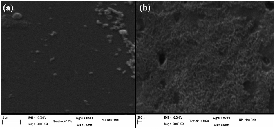 | ||
| Fig. 1 SEM images for (a) 3.5 nm and (b) 5.5 nm thick CdTe films. | ||
High resolution transmission electron microscopy (HRTEM) images of nanocrystal ensembles from thermally evaporated films of CdTe on a carbon film coated grid are shown in Fig. 2(a) and (b). Figures show the lattice fringes of the CdTe nanocrystallites clearly. The shapes of the particles are found to be almost round and distributed throughout the film. XRD patterns for the ultra-thin film of CdTe and bulk CdTe powder were measured (as shown in the ESI†). The intensity of the peaks in the diffraction pattern of the CdTe film was found to be very weak. These peaks were indexed according to the JCPDS data (No.15-0770) of the cubic structure of CdTe. XRD peaks in the pattern at 23.84°, 39.37° and 46.51° correspond to the crystal planes (1 1 1), (2 2 0) and (3 1 1), respectively. The corresponding d spacing values are shown in Fig. 2(a) and (b) which match with the values for bulk CdTe powder.
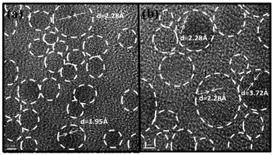 | ||
| Fig. 2 TEM images for (a) 3.5 nm and (b) 5.5 nm thick CdTe films. | ||
Histograms of particle size distribution shown in Fig. 3(a) and (b) were obtained by counting approximately 300 particles in the TEM images shown and in images of nanocrystals obtained on other areas on the grid.
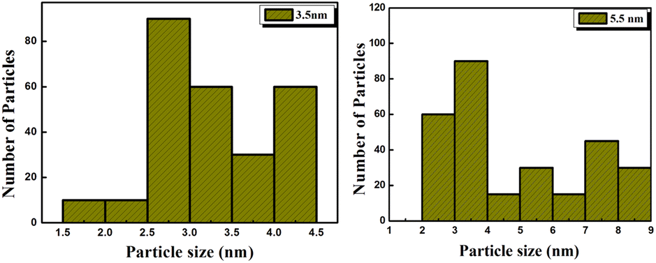 | ||
| Fig. 3 TEM histogram for (a) 3.5 nm and (b) 5.5 nm thick CdTe films. | ||
It was observed that the films consist of randomly oriented fine crystallites of sizes varying between 1.5 nm to 4.5 nm and 2 nm to 9 nm for the 3.5 nm and 5.5 nm thick CdTe films, respectively.
3.2 AFM studies
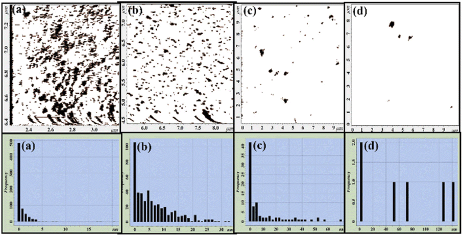
Atomic force microscopy (AFM) is a useful technique to observe high-resolution three-dimensional images of sample surfaces. An AFM instrument probes the sample surface using a cantilever with a sharp tip and measures the changes in force between the probe tip and the sample. Such forces are then measured by the bending of the cantilever as the laser beam is focused on the back of the cantilever and reflected into a photodetector. This instrument has become the most widely used tool for imaging and measuring thin film structures at the nanoscale. Fig. 4 and 5 show the AFM data of the deposited films on glass substrates. The topographical images and the height profiles along the lines drawn in the images are shown in Fig. 4 for (a) 3.5 nm, (b) 5.5 nm, (c) 7.5 nm and (d) 10 nm thick CdTe films. Brighter colours indicate a higher surface. The images clearly depict monolayer islands of nanocrystals of CdTe.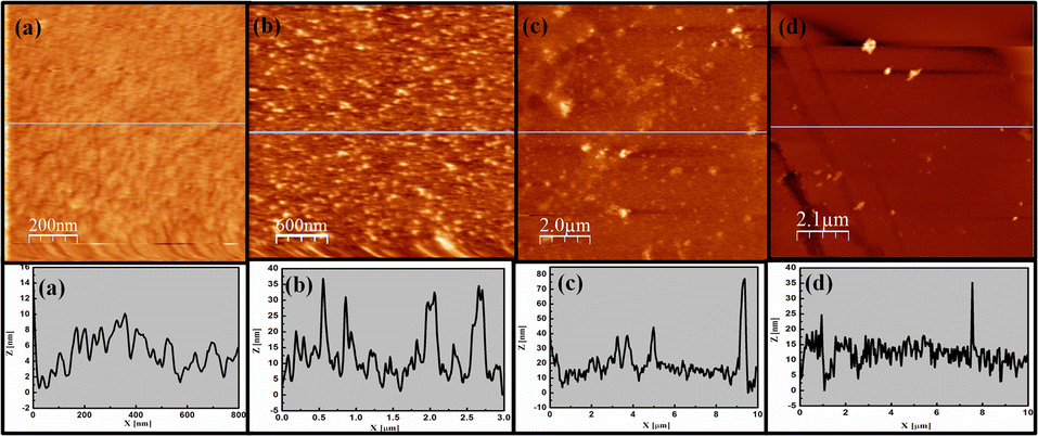 | ||
| Fig. 4 AFM images and the corresponding height profiles for thicknesses of (a) 3.5 nm, (b) 5.5 nm, (c) 7.5 nm and (d) 10 nm. | ||
 | ||
| Fig. 5 Grain analyses and the corresponding size distribution for the thicknesses of (a) 3.5 nm, (b) 5.5 nm, (c) 7.5 nm and (d) 10 nm. | ||
As the film thickness increases, rms roughness values of the films also increase from 2.49 nm to 12.38 nm for the 3.5 nm and 10 nm thick CdTe films, respectively. Fig. 4 also shows the height profiles along the straight lines shown in the images for these thicknesses. Grain analyses and the corresponding size distribution for thicknesses of (a) 3.5 nm, (b) 5.5 nm, (c) 7.5 nm and (d) 10 nm are shown in Fig. 5.
As the film thickness increases, islands grow bigger and particle clustering becomes more prominent. Complete grain analysis data is given in Table 1. As the thickness of the film increases, the number of grains decreases from 678 to only 6, while the average size of a grains increases from 19.72 nm to 46.67 nm for the lowest and highest thicknesses of the film, respectively. Therefore, the microstructural and morphological studies reveal that as the film thickness increases, the average size as well as the rms roughness of the film increases.
| S. No. | Film thickness (nm) | Number of grains | Average size (nm) | rms roughness (nm) |
|---|---|---|---|---|
| A | 3.5 | 678 | 19.72 | 2.49 |
| B | 5.5 | 456 | 21.78 | 7.15 |
| C | 7.5 | 89 | 39.24 | 8.53 |
| D | 10 | 6 | 46.67 | 12.38 |
3.3 UV-Vis and photoluminescence spectra studies
A typical absorption spectrophotometer measures the amount of optical absorption in a material, as a function of wavelength. Whereas, in PL spectroscopy, light of a particular wavelength (usually the peak absorption wavelength) is directed onto a sample, where it is absorbed, and excess energy is imparted to the material. The material then releases the energy absorbed through the emission of light by the process known as photoluminescence. These optical characterizations are useful in determining the electronic structure and properties of materials as they provide the peak light intensity that materials are able to absorb or emit for a certain wavelength. Semiconductor nanocrystals are known to have an absorption edge, which gets shifted towards shorter wavelengths as compared to the bulk material due to size quantization effects. This blue shift is, thus, taken as the indication for the presence of such nanocrystals.CdTe is a direct band gap material which has a band gap energy of ∼1.499 eV. The absorption edge for the bulk hexagonal CdTe is around 826 nm (1.5 eV). The absorption curves from the nanocrystalline thin films (3.5 nm, 5.5 nm, 7.5 nm and 10 nm) of CdTe measured by UV-visible spectrophotometry are shown in Fig. 6(a). From the figure, it is clear that the absorption edge for all the samples is blue shifted as compared to that of bulk CdTe. The absence of a steep onset of absorption in the present case indicates a rather broad band gap distribution and, therefore, a wide particle size distribution. As the bandgap changes with the size, these materials can absorb over a range of wavelengths. Thus, it was not feasible to estimate the particle size distribution from the UV-visible spectra. The blue-shift in the absorption edge indicates an increase in the effective band of the samples. The shift in absorption bands can be understood as the greater the thickness of the CdTe film, the greater the deposition time and, therefore, the bigger the particle in the film.
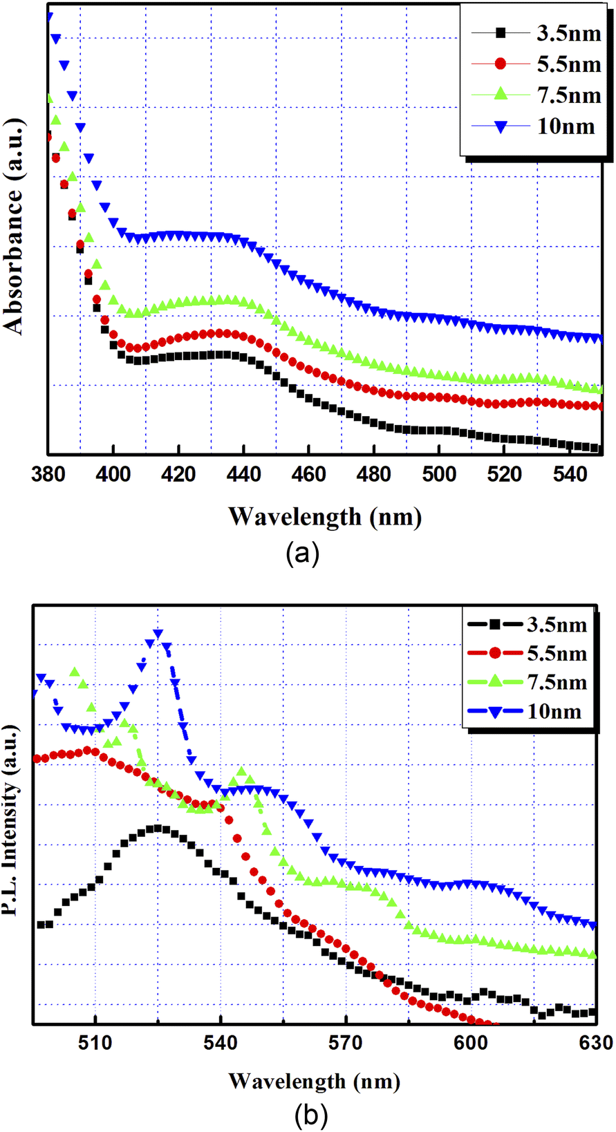 | ||
| Fig. 6 (a) UV-absorption and (b) photoluminescence spectra for the thin films of CdTe. | ||
PL emissions from the nanocrystals (excited at 375 nm) for the 3.5 nm, 5.5 nm, 7.5 nm and 10 nm thick CdTe films on glass substrates are shown in Fig. 6(b). The PL emission peaks were also found to be broad, covering a range of wavelengths from 505 nm to 610 nm, which can be attributed to a large distribution in the particle sizes in the films, as was also observed in microstructural analyses. As the film thickness increases, although broad, the PL emission peaks shift towards higher wavelengths. Increased thicknesses of the films exhibited a large size distribution covering a greater range of particle sizes and hence a greater range of emission wavelengths as compared to the thinner films.
3.4 Electroluminescence studies
To study the electroluminescent properties of the thin films of CdTe, OLEDs with the following device structures were fabricated (the device structure is shown in Fig. 7).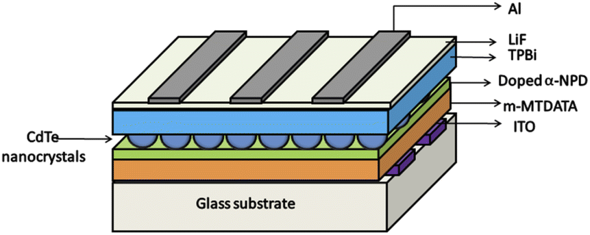 | ||
| Fig. 7 Device structure of the fabricated OLED. | ||
Device (1): ITO/m-MTDATA (20 nm)/doped α-NPD (10 nm)/TPBi (35 nm)/LiF (1 nm)/Al.
Device (2): ITO/m-MTDATA (20 nm)/doped α-NPD (10 nm)/CdTe (x nm)/TPBi (35 nm)/LiF (1 nm)/Al.
Where x= (a) 3.5 nm, (b) 5.5 nm, (c) 7.5 nm and (d) 10 nm.
Fig. 8(a) shows the comparative EL spectra for these devices. The control structure with no CdTe film (device (1)) exhibited two EL peaks at the wavelengths of 445 nm and 480 nm, respectively, which can be attributed to the EL from the organic layers used in the device.
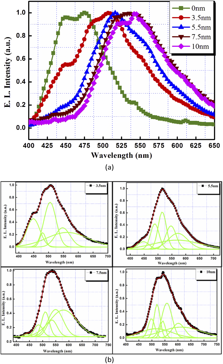 | ||
| Fig. 8 (a) Electroluminescence spectra and (b) deconvoluted electroluminescence spectra for the devices incorporating thin films of CdTe. | ||
For the devices with thin layers of CdTe, broad electroluminescence was observed, as in the PL spectra. Most nanocrystal-based EL devices using organic charge transport layers show emission from both the nanocrystal and polymer layers, due to electron hole recombination in both the components.10,28–30 Therefore, to better resolve the spectra into different peaks, EL spectra were deconvoluted using Gaussian line shape functions, as shown in Fig. 8(b). The devices with ultra-thin layers of CdTe as the emissive layer exhibited EL from organic materials (around 445 nm, 480 nm), as well as new EL peaks identified for different thicknesses as:
(a) CdTe 3.5 nm: 448 nm, 480 nm, 505 nm, 547 nm and 562 nm.
(b) CdTe 5.5 nm: 447 nm, 488 nm, 515 nm, 546 nm, 568 nm and 571 nm.
(c) CdTe 7.5 nm: 440 nm, 484 nm, 510 nm, 535 nm, 549 nm and 579 nm.
(d) CdTe 10 nm: 500 nm, 517 nm, 520 nm, 542 nm, 558 nm, 602 nm and 615 nm.
Therefore, the resulting EL peaks were found to be quite broad, as was also found in the case of the PL spectra of the same thicknesses. When CdTe is incorporated into the EL device, the device emission colour also changes from deep blue (device (1)) to yellow (device (2) with x = 7.5 nm) as shown in Fig. 9. CdTe film thicknesses higher than 10 nm were also tested in these OLEDs to function as an inorganic emissive layer (figure not shown here), but no further shift in EL wavelengths was obtained.
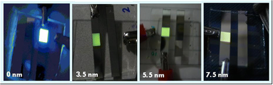 | ||
| Fig. 9 Device photographs exhibiting variations in emission colour and intensity with thickness. | ||
Further, as the CdTe film thickness increases from 3.5 nm to 10 nm, EL peaks shift towards higher wavelengths. This can be understood as an increase in particle size with the increase in film thickness (although the size distribution was broad) and, consequently, the decrease in the bandgap of the CdTe nanocrystals. In addition, as the film thickness increases from 3.5 nm to 10 nm, there is a greater probability of recombination inside the CdTe films. This can be seen in the deconvoluted EL curves of the device with a 10 nm thick CdTe film where no contribution of organic layers is obtained. Therefore, as the CdTe nanocrystals were introduced into the matrix, the emission contribution from the organic molecules decreased and finally diminished when the CdTe film thickness was raised to 10 nm, indicating a direct carrier injection or energy transfer from the organic layers into the CdTe nanocrystals, followed by exciton formation and recombination. This may be due to the trapping of charge carriers by the traps generated by these nanocrystals. Further, the ultra-thin layers of CdTe were sandwiched inside the thick and amorphous layers of ETL and HTL, therefore, the leakage current should not play a significant role in the devices. Also, the incorporation of nanocrystals of CdTe does not show any substantial increase in the current density of these devices as compared to the device having no CdTe film, indicating that there is no substantial contribution of leakage current due to the addition of these layers.
Electroluminescence characterization of OLEDs were performed as tabulated in Table 2. When CdTe is incorporated inside the device, luminance (at 10 V) first increases from 229 Cd m−2 for the control device to 644 Cd m−2 for the device with a 3.5 nm thick CdTe film, and finally decreases to 209 Cd m−2, 148 Cd m−2 and 58 Cd m−2 for the devices with 5.5 nm, 7.5 nm and 10 nm thick CdTe films, respectively. Similarly, the turn-on voltage for the devices first decreased from 5 V for device (1) (with no CdTe film at all) to 3 V for the device with a 3.5 nm thick CdTe film, and then constantly increased to 4 V, 4.6 V and 4.6 V for the devices with 5.5 nm, 7.5 nm and 10 nm thick CdTe films, respectively. Fig. 10(a) and (b) show curves of the current efficiency against voltage and the power efficiency against voltage of the devices, respectively. It can be seen that the incorporation of 3.5 nm CdTe thin films increases the efficiency of the devices, but higher thicknesses of this layer finally decrease the device performance.
| S. No. | CdTe thickness (nm) | Turn-on voltage (V) | Luminance (Cd m−2) at 10V | Current efficiency (Cd A−1) at 10V | Power efficiency (lm W−1) at 10 V |
|---|---|---|---|---|---|
| 1 | 0 | 5 | 229 | 0.1 | 0.03 |
| 2 | 3.5 | 3 | 644 | 1.0 | 0.3 |
| 3 | 5.5 | 4 | 209 | 0.3 | 0.09 |
| 4 | 7.5 | 4.6 | 148 | 0.13 | 0.04 |
| 5 | 10 | 4.6 | 58 | 0.15 | 0.04 |
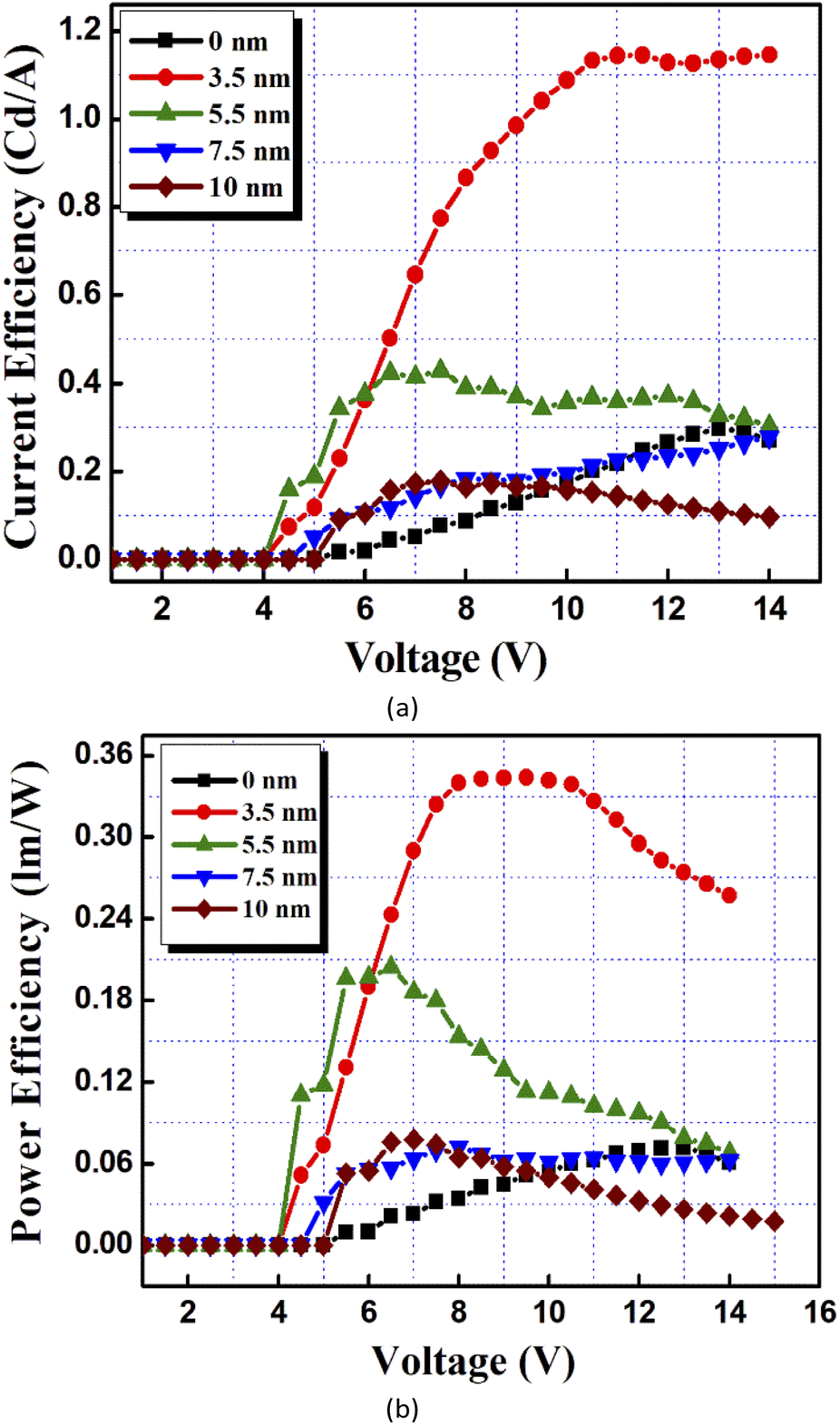 | ||
| Fig. 10 (a) Current efficiency and (b) power efficiency curves for the hybrid organic–inorganic LEDs incorporating the thin films of CdTe. | ||
The current efficiency value achieved at 10 V with device (1) was 0.1 Cd A−1 as compared to 1 Cd A−1, 0.3 Cd A−1, 0.13 Cd A−1 and 0.15 Cd A−1 for the devices with 3.5 nm, 5.5 nm, 7.5 nm and 10 nm thick CdTe films, respectively. Similar results were obtained for the power efficiency of the devices incorporating thin CdTe films, as shown in Table 2. The power efficiency values achieved at 10 V were 0.03 lm W−1 for device (1) as compared to 0.3 lm W−1, 0.09 lm W−1, 0.04 lm W−1 and 0.04 lm W−1 for the devices with 3.5 nm, 5.5 nm, 7.5 nm and 10 nm thick CdTe films, respectively.
This decrease in the efficiency of the device as the CdTe film thickness increases can be attributed to the increased roughness of the thicker CdTe films. AFM analysis of the CdTe films shows that as the thickness increases, and the clustering of the crystallites increase which, in turn, is responsible for the increased roughness and irregular morphology of the thicker films. This results in a higher interfacial resistance and the working voltage of the device becomes higher. Together with the enhanced probability of recombination inside the thick CdTe layers, the films also develop some pin holes or discontinuities in them, as observed from SEM images. This further decreases the efficiency of the devices as the thickness of the CdTe layer increases beyond 3.5 nm. Therefore, the 3.5 nm thick CdTe film provides a higher efficiency of the device as compared to other devices.
Hence the insertion of thin CdTe layer films inside the OLED structure improves the overall performance of the device as compared to the device without the CdTe film. The results indicate the possibility and new way of incorporating thermally evaporated CdTe nanocrystals inside standard OLED structures, which can be further optimized and improved for better performance.
4. Conclusion
Ultra-thin CdTe films were deposited using vacuum thermal evaporation of the bulk CdTe powder. The films were characterised using various techniques and were found to be composed of randomly distributed nanocrystals of CdTe. These ultra-thin films were successfully incorporated inside the standard OLED devices to function as emissive layers. A shift in the EL peak of approximately 40 nm was observed as the thickness of the film increased from 3.5 nm to 10 nm. The device with a 3.5 nm thick CdTe film exhibited the highest efficiency as compared to the devices with thicker films of CdTe, which was attributed to the finest morphology of the 3.5 nm thick CdTe film as compared to the thicker films. Although a saturated emission could not be obtained at either thickness due to a large size distribution of the nanocrystals in the thin films of CdTe, it was demonstrated that ultra-thin films prepared by a convenient thermal evaporation method can easily be employed to fabricate hybrid inorganic–organic LEDs, and the emission properties can be controlled by varying the thickness of the nanocrystalline CdTe film.Author contributions
Conceptualization, R. G.; validation, R. S. and K. S.; writing-original draft preparation, R. G.; writing-review and editing, R. G.; supervision, R. S. and K.·S.Conflicts of interest
There are no conflicts to declare.Acknowledgements
The authors are grateful to Dr Ashok K. Chauhan, Founder President, and Dr V. K. Jain, Distinguished Scientist and Professor, Amity University, Noida, India.References
- M. Naushad, G. Sharma and Z. A. Alothman, J. Cleaner Prod., 2019, 241, 118263 CrossRef CAS.
- A. Mittal, M. Naushad, G. Sharma, Z. A. ALothman, S. M. Wabaidur and M. Alam, Desalin. Water Treat., 2016, 57(46), 21863 CrossRef CAS.
- A. A. Alqadami, M. A. Khan, M. R. Siddiqui and Z. A. Alothman, Microporous Mesoporous Mater., 2018, 261, 198 CrossRef.
- I. Ali, O. M. L. Alharbi, Z. A. Alothman, A. M. Al-Mohaimeed and A. Alwarthan, Environ. Res., 2019, 170, 389 CrossRef CAS PubMed.
- Z. A. Alothman, A. H. Bahkali, M. A. Khiyami, S. M. Alfadul, S. M Wabaidur, M. Alam and B. Z. Alfarhan, Sep. Sci. Technol., 2020, 55(10), 1766 CrossRef CAS.
- Z. A. ALOthman, Materials, 2012, 5, 2874 CrossRef CAS.
- M. A. Khan, A. A. Alqadami, S. M. Wabaidur, M. R. Siddiqui, B. H. Jeon, S. A. Alshareef, Z. A. Alothman and A. E. Hamedelniel, J. Hazard. Mater., 2020, 400, 123247 CrossRef CAS.
- R. Grover, N. Gupta, O. Nanda and K. Saxena, Aligned Zinc Oxide Nanostructures for Dye-Sensitized Solar Cells: A Review, Advances in Solar Power Generation and Energy Harvesting, ed. V. Jain, V. Kumar and A. Verma, Springer Proceedings in Energy. Springer, Singapore, 2020, DOI: DOI:10.1007/978-981-15-3635-9_2.
- S. Liu, S. W. Liu, J. Heng, W. Zhou, Y. Chen, S. Wen, D. Qin, L. Hou, D. Wang and H. Xu, Coatings, 2018, 8, 26 CrossRef.
- A. M. Kadim, Nanomaterials - Toxicity, Human Health and Environment, IntechOpen, London, United Kingdom, 2019, https://www.intechopen.com/chapters/67573.Applications of Cadmium Telluride (CdTe) in Nanotechnology Search PubMed.
- Sh. G. El-sherbiny, S. Wageh, S. M. Elhalafawy and A. A. Sharshar, J. Lumin., 2000, 132, 1957 CrossRef.
- S. Pandey, D. Mukherjee, P. Kshirsagar, C. Patra and D. Bodas, Mater. Today Bio, 2021, 11, 100123 CrossRef CAS PubMed.
- F. Hu, Y. Ran, Z. Zhou and M. Gao, Nanotechnology, 2006, 17, 2972 CrossRef CAS.
- D. Wang, R. Yang, L. Wu, K. Shen and D. Wang, Sol. Energy, 2018, 162, 637 CrossRef CAS.
- Y. Luo, T. Tan, S. Wang, R. Pang, L. Jiang, D. Li, J. Feng, H. Zhang, S. Zhang and C. Li, ACS Appl. Nano Mater., 2022, 5, 401 CrossRef CAS.
- J. Schneider, T. Dudka, Y. Xiong, Z. Wang, N. Gaponik and A. L. Rogach, J. Phys. Chem. C, 2018, 122, 13391 CrossRef CAS.
- A. Shavel, N. Gaponik and A. Eychmüller, J. Phys. Chem. B, 2006, 110, 19280 CrossRef CAS PubMed.
- F. Wang, S. Javaid, W. Chen, A. Wang, M. A. Buntine and G. Jia, Aust. J. Chem., 2021, 74, 179 CrossRef CAS.
- S. M. Farkhani and A. Valizadeh, IET Nanobiotechnol., 2014, 8, 59 CrossRef CAS PubMed.
- S. Chander and M. S. Dhaka, J. Mater. Sci.: Mater. Electron., 2016, 27, 11961 CrossRef CAS.
- S. Chander, A. Purohit, C. Lal and M. S. Dhaka, Mater. Chem. Phys., 2017, 185, 202 CrossRef CAS.
- T. Ablekim, J. N. Duenow, X. Zheng, H. Moutinho, J. Moseley, C. L. Perkins, S. W. Johnston, P. O'Keefe, E. Colegrove, D. S. Albin, M. O. Reese and W. K. Metzger, ACS Energy Lett., 2020, 5, 892 CrossRef CAS.
- S. M. Wabaidur, G. E. Eldesoky and Z. A. Alothman, Luminescence, 2018, 33(3), 625 CrossRef CAS PubMed.
- S. M. Wabaidur, S. M. Alam, Z. A. Alothman and K. Mohsin, Spectrochim. Acta, Part A, 2015, 144, 170 CrossRef CAS.
- R. Grover, R. Srivastava, O. Rana, A. K. Srivastava, K. K. Maurya, K. N Sood, D. S. Mehta and M. N. Kamalasanan, J. Lumin., 2012, 132, 330 CrossRef CAS.
- R. Kumar, R. Srivastava and P. Singh, J. Semicond., 2016, 37, 013001 CrossRef.
- E. Talha and D. H. Volkan, Nanophotonics, 2013, 2, 57 Search PubMed.
- G. Zaiats, S. Ikeda and P. V. Kamat, NPG Asia Mater., 2020, 12, 57 CrossRef CAS.
- A. M. Kadim, J. Nano Res., 2017, 50, 48 CAS.
- H. H. Kim, J. S. Park, I. K. Han, S. O. Won, C. Park, D. K. Hwang and W. K. Choi, Nanoscale, 2016, 8, 19737 RSC.
Footnote |
| † Electronic supplementary information (ESI) available. See https://doi.org/10.1039/d2ra01387h |
| This journal is © The Royal Society of Chemistry 2022 |