
 Open Access Article
 This Open Access Article is licensed under a Creative Commons Attribution-Non Commercial 3.0 Unported Licence
Enhanced power conversion efficiency of an n-Si/PEDOT:PSS hybrid solar cell using nanostructured silicon and gold nanoparticles
Pham Van Trinh *ab,
Nguyen Ngoc Anha,
Nguyen Thi Chamc,
Le Tuan Tuc,
Nguyen Van Haod,
Bui Hung Thanga,
Nguyen Van Chuca,
Cao Thi Thanha,
Phan Ngoc Minhab and
Naoki Fukatae
*ab,
Nguyen Ngoc Anha,
Nguyen Thi Chamc,
Le Tuan Tuc,
Nguyen Van Haod,
Bui Hung Thanga,
Nguyen Van Chuca,
Cao Thi Thanha,
Phan Ngoc Minhab and
Naoki Fukatae
aInstitute of Materials Science, Vietnam Academy of Science and Technology, 18 Hoang Quoc Viet Str., Cau Giay Distr., Hanoi, Vietnam. E-mail: trinhpv@ims.vast.vn; Tel: +84 943190301
bGraduate University of Science and Technology, Vietnam Academy of Science and Technology, 18 Hoang Quoc Viet Str., Cau Giay Distr., Hanoi, Vietnam
cVNU University of Science, Vietnam National University, 334 Nguyen Trai Str., Thanh Xuan Distr., Hanoi, Vietnam
dFaculty of Physics and Technology, TNU-University of Sciences, Tan Thinh Ward, Thai Nguyen City, Vietnam
eInternational Center for Materials Nanoarchitectonics, National Institute for Materials Science, 1-1 Namiki, Tsukuba, Ibaraki 305-0044, Japan
First published on 5th April 2022
Abstract
Herein, the effect of nanostructured silicon and gold nanoparticles (AuNPs) on the power conversion efficiency (PCE) of an n-type silicon/poly(3,4-ethylene dioxythiophene):poly(styrene sulfonate) (n-Si/PEDOT:PSS) hybrid solar cell was investigated. The Si surface modified with different nanostructures including Si nanopyramids (SiNPs), Si nanoholes (SiNHs) and Si nanowires (SiNWs) was utilized to improve light trapping and photo-carrier collection. The highest power conversion efficiency (PCE) of 8.15% was obtained with the hybrid solar cell employing SiNWs, which is about 8%, 20% and 40% higher compared to the devices using SiNHs, SiNPs and planar Si, respectively. The enhancement is attributed to the low reflectance of the SiNW structures and large PEDOT:PSS/Si interfacial area. In addition, the influence of AuNPs on the hybrid solar cell's performance was examined. The PCE of the SiNW/PEDOT:PSS hybrid solar cell with 0.5 wt% AuNP is 8.89%, which is ca. 9% higher than that of the device without AuNPs (8.15%). This is attributed to the increase in the electrical conductivity and localized surface plasmon resonance of the AuNP-incorporated PEDOT:PSS coating layer.
1. Introduction
Currently, solar cells using bulk silicon materials have been used as commercial products.1–3 However, the surface of bulk silicon has high reflectivity under the solar radiation leading to most incident light being reflected; as a result, the PCE of the solar cell is low. Therefore, reducing the reflectivity of silicon has received considerable attention from researchers.4 In order to address this issue, one of the promising methods is fabricating nanostructured silicon.5–7 Indeed, the silicon nanostructure could achieve near-zero anti-reflection over a broad wavelength.8 Moreover, these silicon nanostructures have the ability to trap the incident light and suppress the surface reflection, which is good for photovoltaic devices.9,10 In addition, the silicon nanostructures increase the light absorption ability owing to a large surface area in comparison with bulk silicon.11–14 There are two general approaches to fabricate silicon nanostructures, namely top-down and bottom-up. Several bottom-up methods have been carried out to fabricate silicon nanostructures, such as the chemical vapor deposition method, molecular beam epitaxy technique, and thermal evaporation method.15–17 However, these methods are often difficult to perform due to the complex and expensive equipment are required. The top-down methods are widely used in industry as they are easier and much cheaper than the bottom-up methods. There are three main top-down methods: photolithography, dry etching and wet chemical etching.18–21 Among these top-down methods, photolithography and dry etching are time-consuming and expensive methods, whereas wet chemical etching is simple to perform with low cost. In addition, wet chemical etching is suitable for high quantity production with a large uniform structure.Recently, the hybrid solar cells have been attracting research attention due to their great potential in terms of performance and production costs.1,2,22 The hybrid solar cell structure combines organic and inorganic materials to take advantage of some of the unique properties of both materials.22 The commonly used organic materials are conductive polymers, such as PEDOT:PSS, for the production of hybrid solar cells. In the hybrid structure, PEDOT:PSS acts as a p-type semiconductor and is deposited on top of an inorganic material as an n-type semiconductor (i.e. n-type Si) to create a p–n junction. Si/PEDOT:PSS hybrid solar cells have been developed by some research groups and are expected to replace the current solar cell generations based on bulk silicone materials and solar thin-film. Some serious issues such as the defects in the PEDOT:PSS/Si interface, small p–n junction areas, low optical absorption and carrier recombination could be the major barriers causing the negative effects on the efficiency of the hybrid solar cells.22 There are several proposed approaches to solve the above problems, such as using three-dimensional (3D) Si nanostructures (SiNW, SiNH, SiNPs), to improve the p–n junction area and the optical adsorption, and to add guest materials (AuNPs, Si quantum dots, graphene, graphene quantum dots) to improve the optoelectrical properties of the conductive polymer materials.23–29 However, most of the published works only focused on using single Si nanostructures to enhance the PCE of the fabricated solar cells. There are no papers published to compare the performance among them. Moreover, the presence of metallic nanoparticles (i.e. AuNPs, AgNPs), which acts as plasmonic factors inside the organic layer, has also received considerable attention due to being a potential solution for enhancing the performance of the solar cells.27–33
Thus, in this study, both Si surface modification and AuNP addition were used to improve the PCE of the hybrid solar cells resulting from the reduction in reflectance and the increase in plasmonic effects. The chemical reduction approach was used to prepare AuNPs (∼17 nm) that served as plasmonic enhancement factors. The Si surface was chemically etched to produce three Si nanostructures including SiNPs, SiNHs, and SiNWs, which were then employed as the substrates to compare their effects on the light trapping and the efficiency of the fabricated hybrid solar cells.
2. Experimental
2.1. Materials
Silicon n-type (thickness 525 ± 5 μm, resistivity 1–10 Ω) were purchased from SEHOUNG Wafertech, Korea. Acetone, iso-propanol (IPA), HF, H2SO4 (98%), HNO3 (68%), H2O2, KOH, NaBH4 and AgNO3 were purchased from Shantou Xilong, China. Chloroauric acid (HAuCl4) was purchased from Aldrich-Sigma for synthesizing AuNPs.2.2. Preparation of Si nanostructures
First, the Si substrate was pretreated to remove all the contaminants by ultrasonication in acetone for 5 min and then in isopropanol for 5 min. As a result, the organic contaminant is removed. Second, the inorganic contaminant, together with dust and small-unwashed particles, is removed by ultrasonication in DI water for 5 min. These two steps were repeated three times. Third, the wafer was immersed in piranha solution (H2SO4![[thin space (1/6-em)]](https://www.rsc.org/images/entities/char_2009.gif) :H2O2 4:1) at 140 °C for 10 min. Finally, the Si substrate was cleaned again by DI water then dried under nitrogen gas for preparing Si nanostructures including SiNWs, SiNHs and SiNPs, as shown in Fig. 1.
:H2O2 4:1) at 140 °C for 10 min. Finally, the Si substrate was cleaned again by DI water then dried under nitrogen gas for preparing Si nanostructures including SiNWs, SiNHs and SiNPs, as shown in Fig. 1.
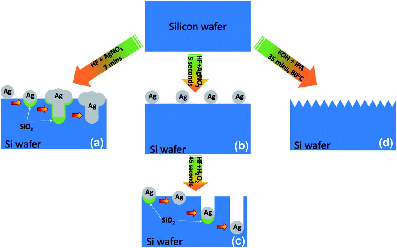 | ||
| Fig. 1 Schematic of the fabrication of: (a) SiNWs, (b and c) SiNHs and (d) SiNPs. | ||
At the cathode:
| Ag+ + e− → Ag |
At the anode:
| Si + 2H2O + 4H+ → SiO2 + 4H+ |
| SiO2 + HF → H2SiF6 + 2H2O |
The complete redox reaction:
| Si + 4Ag+ + 6 HF → 4Ag + H2SiF6 + 4H+ |
In this method, Ag+ was reduced to Ag and deposited on the surface of the Si substrate. The surface silicon atoms were oxidized by releasing an electron or consuming a hole. Subsequently, the silicon oxide was etched by the HF solution, leaving pits on the surface. The Ag nanoparticles that are trapped in these pits continue to sink downward by a continuous process of galvanic displacement of Si.35 After the etching process, the SiO2 layer was removed by HF 5% solution. The excess ions Ag+ and the residual Ag nanoparticles were rinsed with DI water three times for 10 min and then dried with nitrogen gas.
| Si + KOH → K2SiO3 + H2 |
The hydrogen bubbles are released during the anisotropic etching of silicon by KOH, as shown in the equation above. These H2 bubbles tend to stick to the silicon surface, which acts as a local mask to prevent texturing at those positions resulting in a non-homogeneous texture. The IPA enhances the wet ability of the Si surface by lowering surface tension and effectively removing the H2 bubbles.36,37
2.3. Synthesis of AuNPs
The chemical reduction method was used to prepare AuNPs. A NaBH4 (0.1 M) solution was added in 100 mL HAuCl4 (0.2 mM) and magnetically stirred continuously at 600 rpm until the color of the solution changes from yellow to dark red. Then, the as-prepared AuNP solution was centrifuged at 10000 rpm for 10 min and dispersed in deionized water by ultrasonic to prepare an AuNP solution with a concentration of 1 mg/1 mL.
2.4. Fabrication of hybrid solar cell
First, Si substrates modified with different Si nanostructures (SiNWs, SiNHs, and SiNPs) were cleaned with the piranha solution at 130 °C for 40 min and several times with DI water. The Si substrate was submerged in a 2% HF solution for 1 min and coated immediately by a highly conductive polymer comprising PEDOT:PSS, 5% DMSO and 0.1 wt% Zonyl® fluorosurfactant at a speed of 2000 rpm (10 s), followed by an increase to 6000 rpm (60 s). After that, the hybrid structures were annealed at 140 °C for 30 min. For the hybrid solar cell containing AuNPs, 0.5 wt% AuNP was added in the high conductive polymer by ultrasonication and then spin-coated on the surface of the Si nanostructure. Finally, the back electrode was formed by depositing a thin film of 50 nm Ti and 200 nm Ag, and the front electrode contact was made by a finger-typed 250 nm Ag-film.2.5. Characterizations
Field emission scanning electron microscopy was performed to study the morphology of the specimens (FESEM, Hitachi S4800). A JASCO V-770 spectrophotometer was used to obtain the reflectance and absorption spectra. The 4-point technique (Sigma-5+, NPS Inc, Japan) was employed to measure the sheet resistance thin film. A spectral response measurement was used to record the external quantum efficiency (EQE) spectra at wavelengths ranging from 300 to 1100 nm. The PCE of the as-prepared solar cells was determined using a Keithley 2400 source meter under air mass 1.5 global (AM 1.5G) illumination (100 mW cm−2).3. Results and discussions
3.1. Morphology of silicon nanostructures
Fig. 2(a1) and (a2) show the microstructure of the as-prepared SiNPs. As observed, the pyramids in various sizes ranging from 0.2 to 2.5 μm covered the whole surface. This observation could be attributed to the evaporation of IPA during the etching process. The evaporation of iso-propanol leads to the reduction in the concentration of IPA during the etching process, leading to the decrease in the uniformity of the etching process. The surface area of SiNP arrays was estimated by the statistical calculation of SEM images. The top view and cross-section of the SiNH structures are shown in Fig. 2(b1) and (b2), respectively. The whole surface of the Si substrate was covered with silicon nanoholes with an average of roughly 40 nm in diameter and 680 nm in depth. There are presence of some holes that were bent to the left direction, as shown in Fig. 2(b2), suggesting that the Ag nanoparticles changed their direction movement in silicon during the etching process. Fig. 2(b2) not only shows the vertical holes according to the (100) direction but also the horizontal holes according to the (010), (0−10), (001) and (00−1) directions, which are equivalent to the (100) direction. This bending phenomenon could be due to the semispherical side of Ag nanoparticles. It is interesting to note that the absence of AgNPs indicated that the remaining AgNPs were entirely eliminated after the washing processes. The SiNW structure obtained by the one-step etching process is shown in Fig. 2(c1) and (c2). The SiNW array with a length of 720 nm covered the entire Si substrate uniformly. These SiNWs were formed as bundle-like structures due to the van der Waals force between nanowires.38 From the top view image, the different distances between SiNW arrays were observed. This could be due to the agglomeration and/or different sizes of Ag nanoparticles, which acted as the catalyst and reactive places for the etching process.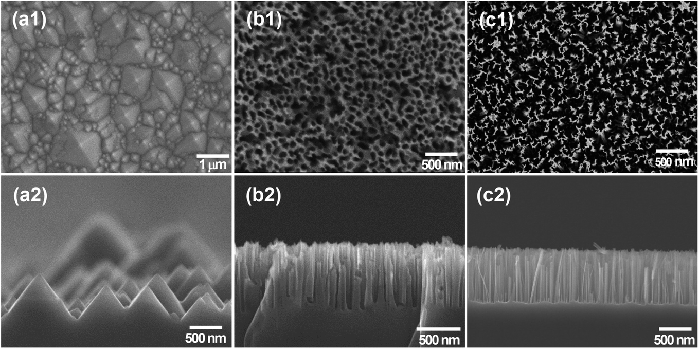 | ||
| Fig. 2 SEM images of the top-viewed and cross sectional viewed (a1 and a2) SiNPs, (b1 and b2) SiNHs and (c1 and c2) SiNWs. | ||
The microstructure of the Si substrate modified with different nanostructures after coating with PEDOT:PSS is shown in Fig. 3. For SiNPs, the conductive polymer was entirely coated on top of the SiNPs. However, the narrow gaps among SiNPs were not penetrated completely by PEDOT:PSS (Fig. 3a). For SiNHs, as observed in Fig. 3b, the PEDOT:PSS was not only thoroughly coated on top of SiNHs but also penetrated fully into the holes. This indicates that the applied spin-coating condition is suitable for fabricating uniform SiNHs/PEDOT:PSS hybrid structures. For SiNWs, the Si/PEDOT:PSS hybrid structures were also prepared, and single SiNW was coated and covered with PEDOT:PSS. The fabrication of homogenous Si/PEDOT:PSS hybrid structures might be a beneficial factor to enhance hybrid solar cell performance.
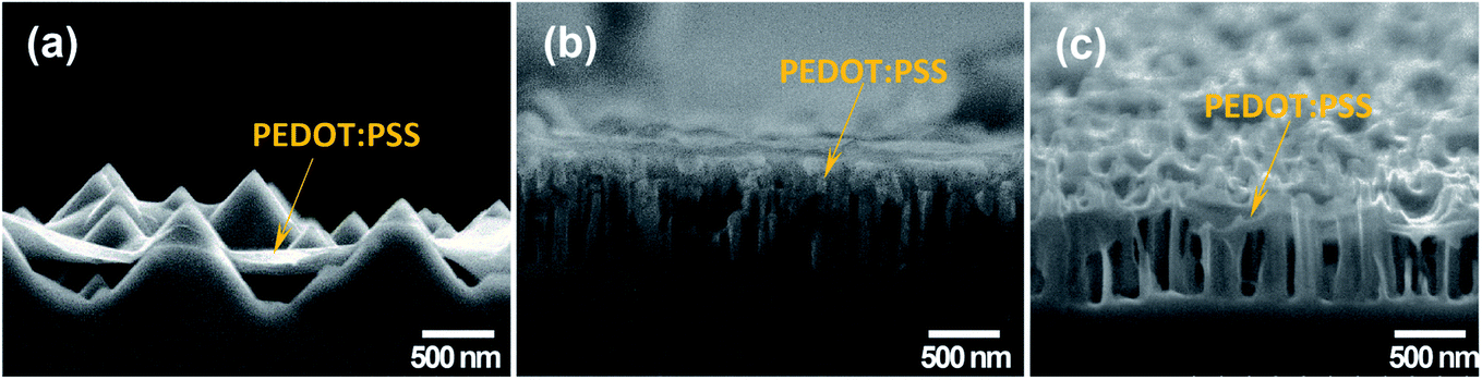 | ||
| Fig. 3 SEM images of (a) SiNPs, (b) SiNHs and (c) SiNWs after PEDOT:PSS coating. | ||
The reflectance spectra in the incident wavelength range 500–1200 nm of planar Si and Si substrates modified with SiNPs, SiNHs and SiNWs are shown in Fig. 4. As can be observed, the reflectance of the planar Si substrate was below 40% and then reduced to 20% for SiNPs. As a result, the reflectance of SiNPs decreased compared to that of the planar Si substrate. The reflectance of the Si substrate significantly reduced when modified with SiNH and SiNWs. The reflectance was determined to be below 10% for both structures. In addition, in the incident wavelength ranging of 300–700 nm, the reflectance of SiNWs exhibited a significant drop of less than 7%. These results indicated that Si substrates modified with nanostructures such as SiNPs, SiNHs, and SiNWs could provide an antireflection substrate by lengthening the effective optical path length of incident light due to light trapping and light scattering.
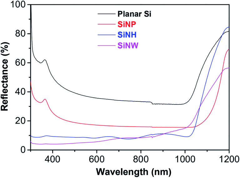 | ||
| Fig. 4 Reflectance spectra of planar Si, SiNPs, SiNHs and SiNWs in the incident wavelength range from 500 to 1200 nm. | ||
The parameters of the as-prepared hybrid solar cell are presented in Fig. 5a and Table 1. Fig. 5 shows the current density–voltage (J–V) characteristics and energy diagram of PEDOT:PSS/Si hybrid solar cells. In this structure, the n-type Si acted as the n-type semiconductor material, the light absorbing layer and the electron-holepairs generating component. The PEDOT:PSS layer operates as the p-type semiconductor material and the hole transport layer. The separation process of the electron–hole pairs occurred at the Si/PEDOT:PSS interfaces (Fig. 5b). The devices that used planar Si substrates had a low performance with a PCE of 5.81%, a Jsc of 25.01 mA cm−2, a Voc of 0.484 V and an FF of 0.48%. The low PCE of the device using planar Si can be due to the high reflectance and small p/n junction area formed by n-Si and PEDOT:PSS (Fig. 5a). The PCE of the devices using SiNPs (6.75%) was enhanced up to 16% compared to the planar Si hybrid solar cell with a Jsc of 25.27 mA cm−2, a Voc of 0.504 V and an FF of 53%. It is worth noting that the performance of the hybrid solar cells was significantly increased when SiNHs and SiNWs were used. The values of the PCE were measured to be 7.53% and 8.15% corresponding to the devices using SiNHs and SiNWs, respectively. The device using SiNWs shows the best performance, which is about 8%, 20% and 40% improvement in the PCE compared to the devices using SiNHs, SiNPs and planar Si, respectively. The enhancement could result from the low reflectance of SiNW structures for enhancing the light absorption and to large p/n junction areas for enhancing the carrier collection efficiency.39–44 Moreover, the increase in the surface roughness of the devices using SiNWs is shown in Fig. 3c. According to several reports, the surface roughness increased leading to the reduction in the hole extraction path and the improvement in the hole collection efficiency, and thus the PCE of hybrid solar cells increased.45–48
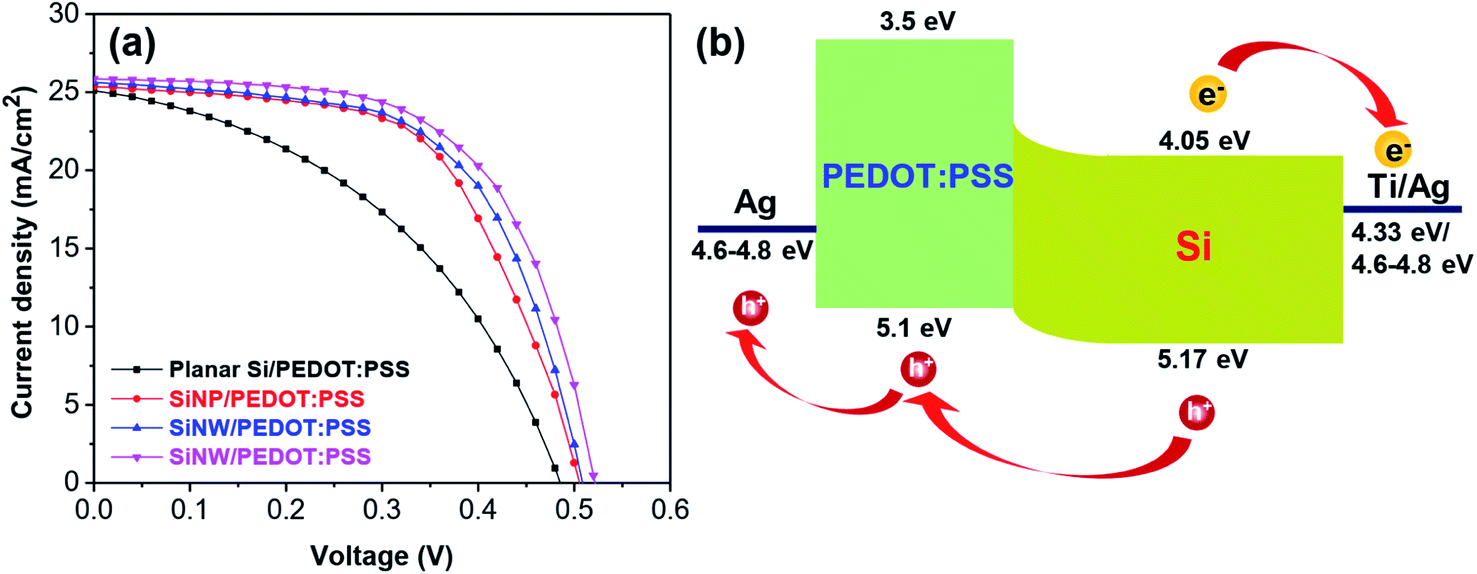 | ||
| Fig. 5 (a) J–V characteristic curves of the hybrid solar cell using planar Si and Si nanostructures and (b) energy diagram of the n-Si/PEDOT:PSS hybrid solar cell. | ||
| No. | Structures | AuNP (wt%) | Jsc (mA cm−2) | Voc (V) | Rs (Ω cm−2) | FF (%) | PCE (%) |
|---|---|---|---|---|---|---|---|
| 1 | Ti/Ag/Planar Si + PEDOT:PSS/Ag | 0 | 25.01 | 0.484 | 5.33 | 48 | 5.81 |
| 2 | Ti/Ag/SiNPs + PEDOT:PSS/Ag | 0 | 25.27 | 0.504 | 4.57 | 53 | 6.75 |
| 3 | Ti/Ag/SiNHs + PEDOT:PSS/Ag | 0 | 25.59 | 0.508 | 2.77 | 58 | 7.53 |
| 4 | Ti/Ag/SiNWs + PEDOT:PSS/Ag | 0 | 25.86 | 0.514 | 2.43 | 61 | 8.15 |
| 5 | Ti/Ag/SiNWs + PEDOT:PSS + AuNP/Ag | 0.5 | 26.23 | 0.531 | 2.12 | 64 | 8.89 |
In order to investigate the effect of AuNPs on the performance of the hybrid solar cells, a concentration of 0.5 wt% AuNP was added in the conducting polymer. AuNPs with an average diameter of 17 nm synthesized by the chemical reduction method was used for the study. The as-prepared AuNPs exhibit an absorption peak at 519 nm, which is assigned to the plasmon resonance absorption of AuNPs (Fig. 6a). The sheet resistance of the PEDOT:PSS/AuNP thin film with a thickness of 50 nm was measured. As a result, the sheet resistance of the PEDOT:PSS/AuNP film was nearly two times lower than that of the pristine PEDOT:PSS thin film (Fig. 6b).
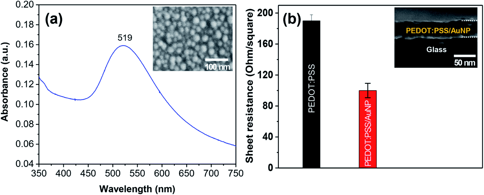 | ||
| Fig. 6 (a) Optical absorption spectra and SEM image of AuNPs synthesized by chemical reduction method (b) sheet resistance of PEDOT:PSS thin films with and without AuNPs. | ||
Fig. 7a shows the structure of SiNW/PEDOT:PSS hybrid solar cell containing AuNPs. The EQE of SiNW/PEDOT:PSS hybrid solar cells containing 0.5 wt% AuNP is shown in Fig. 7b. As a result, the EQE of the hybrid solar cell was improved in a spectrum of 300–600 nm in the presence of AuNPs. The increased EQE might have resulted from the light-trapping effect of AuNPs at wavelengths less than 500 nm and the increase in the optical absorption of the PEDOT:PSS/AuNPs, as discussed in the previous study.25 Furthermore, the presence of AuNPs increased the roughness of the device surface, leading to an increase in EQE.30 Fig. 7c shows the J–V curves of the hybrid solar cells with and without AuNPs. As a result, the performance of the hybrid solar cell containing AuNPs improved compared with the cell without AuNPs. The SiNW/PEDOT:PSS/AuNPs hybrid solar cell has a Jsc of 26.23 mA, a Voc of 0.53, an FF of 0.64 and a maximum PCE of 8.89%, which corresponds to an enhancement of ca. 9% compared to the solar cells without AuNPs (8.15%). The obtained results are in good agreement with other reports.27–30 Lu et al. reported that the PCE of the SiNHs/PEDOT:PSS hybrid solar cell containing AuNPs was determined to be 6.1%, which is an improvement of 27% compared to that of the solar cells without AuNPs.27 Similarly, Sharma et al. also reported a PCE of 8.2% for planar Si/PEDOT:PSS/AuNPs, which is higher than that of the device without AuNPs (7.3%).29 The higher PCE for Si/PEDOT:PSS/AuNP hybrid solar cells was reported by Kim et al. in which a PCE was measured to be 11.19% for the device containing AuNPs by the in situ method, which is approximately 19% higher compared to the device without AuNPs (9.42%).30 Therefore, the incorporation of AuNPs acting as incident light antennas in PEDOT:PSS might improve the performance of hybrid solar cells. The energy might be stored in the localized surface plasmon mode using these antennas. Furthermore, the increase in the electrical conductivity of PEDOT:PSS might be a factor resulting in a higher Voc compared to devices without AuNPs (0.514 V) and consequently a higher PCE.27,29,30 In addition, the increase in PCE could originate from the reduction of the series resistance (Rs) of the device containing AuNPs (2.12 Ω cm2) in comparison with the device without AuNPs (2.43 Ω cm2). According to Otieno et al., the reduction in Rs could be due to the presence of AuNPs, thus leading to the decrease in the work function of the PEDOT:PSS and the decrease of the PEDOT:PSS volume assisting the movement of the holes towards the anode, and thus reduce the effective device resistance.31 The decrease of the Rs encourages the charge collection leading to an increase in the FF from 61 to 64%.49,50 The dark J–V characteristics of the hybrid solar cells with and without AuNPs were shown in Fig. 7d. As a result, the decrease in the leakage current density of the devices confirmed the reduction of the Rs and the increase in the electrical conductivity of PEDOT:PSS caused by adding AuNPs. The hybrid solar cell containing AuNPs exhibited a high current density in forward bias and a better charge collection efficiency, thus leading to the improvement of the PCE.
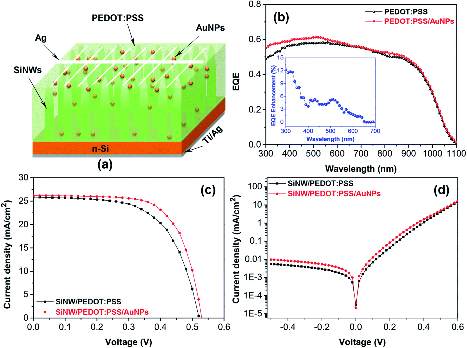 | ||
| Fig. 7 (a) Structure, (b) EQE spectrum, (c) J–V characteristic curves and (d) dark J–V curves of SiNW/PEDOT:PSS/AuNPs hybrid solar cells. | ||
4. Conclusion
We have investigated the effect of nanostructured silicon surface modification and AuNP incorporation in the PEDOT:PSS on the performance of n-Si/PEDOT:PSS hybrid solar cells. The obtained results showed that the hybrid solar cells using nanostructured Si surface modification, such as SiNPs, SiNHs and SiNWs, exhibited a significant improvement in the performance due to the enhancement in light trapping and photo-carrier collection. The highest PCE of 8.15% was obtained with the solar cell using SiNWs as a substrate, which is ca. 40% higher compared to the planar Si solar cell. The hybrid solar cell containing 0.5 wt% AuNPs reached a peak PCE of 8.89%, which shows an improvement of about 9% compared to the device without AuNPs (8.15%). This improvement mainly originated from the increase in electrical conductivity, the reduction in the series resistance and localized surface plasmon resonance of the AuNPs, thus leading to increase FF, Voc and Jsc. Our results suggest that the performance of Si/PEDOT:PSS hybrid solar cells could be improved by the combination of both nanostructured silicon surface modification and AuNP incorporation in the PEDOT:PSS.Conflicts of interest
The authors declare no possible conflict of interests.Acknowledgements
This research is funded by Vietnam National Foundation for Science and Technology Development (NAFOSTED) under grant number 104.06-2018.34.References
- Y. Liu, Y. Li, Y. Wu, G. Yang, L. Mazzarella, P. P. Moya, A. C. Tamboli, K. Weber, M. Boccard, O. Isabella, X. Yang and B. Sun, Mater. Sci. Eng.: R: Reports, 2020, 142, 100579 CrossRef.
- L. L. Yan, C. Han, B. Shi, Y. Zhao and X. D. Zhang, Materials Today Nano, 2019, 7, 100045 CrossRef.
- J. Y. H. Chai, B. T. Wong and S. Juodkazis, Materials Today Energy, 2020, 18, 100539 CrossRef CAS.
- A. J. Baca, K. J. Yu, J. L. Xiao, S. D. Wang, J. Yoon, J. H. Ryu, D. Stevenson, R. G. Nuzzo, A. A. Rockett and Y. G. Huang, Energy Environ. Sci., 2010, 3, 208–211 RSC.
- P. Campbell and M. A. Green, J. Appl. Phys., 1987, 62, 243–249 CrossRef.
- M. K. Sahoo and P. Kale, J. Materiomics, 2019, 5, 34–48 CrossRef.
- S. Kato, Y. Kurokawa, K. Gotoh and T. Soga, Appl. Sci., 2019, 9, 818 CrossRef CAS.
- J. Chen, T. Subramani, W. Jevasuwan, K. C. Pradel and N. Fukata, Nanotechnology, 2019, 30, 344001 CrossRef CAS PubMed.
- S. A. Moiz, A. N. M. Alahmadi and A. J. Aljohani, Energies, 2020, 13(15), 3797 CrossRef.
- T. Subramani, C. C. Hsueh, H. J. Syu, C. T. Liu, S. T. Yang and C. F. Lin, RSC Adv., 2016, 6, 12374–12381 RSC.
- Q. Yang, X. A. Zhang, A. Bagal, W. Guo and C. H. Chang, Nanotechnology, 2013, 24, 235202 CrossRef PubMed.
- R. Venkatesan, J. Mayandi, J. M. Pearce and V. Venkatachalapathy, J. Mater. Sci.: Mater. Electron., 2019, 30, 8676 CrossRef CAS.
- W. Chen and P. R. Cabarrocas, Nanotechnology, 2019, 30, 194002 CrossRef CAS PubMed.
- J. Chen, T. Subramani, W. Jevasuwan, K. Dai, K. Shinotsuka, Y. Hatta and N. Fukata, Nano Energy, 2019, 56, 604–611 CrossRef CAS.
- E. Garnett and P. Yang, Nano Lett., 2010, 10, 1082–1087 CrossRef CAS PubMed.
- R. L. Latu, C. Mouchet, C. Cayron, E. Rouviere and J. P. Simonato, J. Nanopart. Res., 2008, 10, 1287–1291 CrossRef.
- H. Pan, S. Lim, C. Poh, H. Sun, X. Wu, Y. Feng and J. Lin, Nanotechnology, 2005, 16, 417–421 CrossRef.
- S. K. Srivastava, P. K. Singh, V. N. Singh, K. N. Sood, D. Haranath and V. Kumar, Physica E, 2009, 41, 1545–1549 CrossRef CAS.
- J. Mart and R. Garcia, Nanotechnology, 2010, 21, 245301 CrossRef PubMed.
- Y. Q. Fu, A. Colli, A. Fasoli, J. K. Luo and A. J. Flewitt, J. Vac. Sci. Technol. B, 2009, 27, 1520–1526 CrossRef CAS.
- K. Q. Peng, Y. Yan, S. P. Gao and J. Zhu, Adv. Mater., 2002, 14, 1164–1167 CrossRef CAS.
- Z. Sun, Y. He, B. Xiong, S. Chen, M. Li, Y. Zhou, Y. Zheng, K. Sun and C. Yang, Angew. Chem., Int. Ed., 2021, 60, 5036 CrossRef CAS PubMed.
- R. Shen, Z. Sun and Y. Zhou, et al., Prog. Photovolt. Res. Appl., 2022, 1–9, DOI:10.1002/pip.3540.
- S. H. Chen, T. C. Wei, T. Y. Wu and C. Y. Chen, Mater. Lett., 2022, 307, 130967 CrossRef CAS.
- P. V. Trinh, N. N. Anh, N. T. Bac, C. T. Anh, N. V. Hao, L. H. Chi, B. H. Thang, N. V. Chuc, P. N. Minh and N. Fukata, Mater. Sci. Semicond. Process., 2022, 137, 106226 CrossRef.
- N. A. Nguyen, V. H. Nguyen, V. N. Pham, T. T. Le and V. T. Pham, Adv. Natural Sci.: Nanosci. Nanotechnol., 2021, 12(3), 035009 CAS.
- R. Lu, L. Xu, Z. Ge, R. Li, J. Xu, L. Yu and K. Chen, Nanoscale Res. Lett., 2016, 11, 60 CrossRef PubMed.
- M. Sharma, P. R. Pudasaini, F. R. Zepeda, D. Elam and A. A. Ayon, ACS Appl. Mater. Interfaces, 2014, 6, 4356–4363 CrossRef CAS PubMed.
- M. Sharma, R. L. Delgado and A. A. Ayon, Microsyst. Technol., 2018, 24, 543–550 CrossRef CAS.
- W. H. Kim, S. J Sung, K. P. Kim, D. K. Hwang and S. Woo, Sci. Adv. Mater., 2018, 10(4), 560–564 CrossRef CAS.
- F. Otieno, N. P. Shumbula, M. Airo, M. Mbuso, N. Moloto, R. M. Erasmus, A. Quandt and D. Wamwangi, AIP Advances, 2017, 7, 085302 CrossRef.
- E. Susanti, P. Wulandari and Herman, J. Phys.: Conf. Ser., 2018, 1080, 012010 CrossRef.
- O. A. Ghazy, M. M. Ibrahim, F. I. A. Elfadl, H. M. Hosni, E. M. Shehata, N. M. Deghiedy and M. R. Balboul, J. Radiation Res. Appl. Sci., 2015, 8(2), 166–172 CrossRef CAS.
- S. W. Baek, J. Noh, C. H. Lee, B. Kim, M. K. Seo and J. Y. Lee, Sci. Rep., 2013, 3, 1726 CrossRef.
- T. Subramani, C. C. Hsueh, H. J. Syu, C. T. Liu, S. T. Yang and C. F. Lin, RSC Adv., 2016, 6, 12374–12381 RSC.
- S. K. Srivastava, D. Kumar, S. W. Schmitt, K. N. Sood, S. H. Christiansen and P. K. Singh, Nanotechnology, 2014, 25, 175601 CrossRef PubMed.
- M. F. Abdullah, M. A. Alghoul, H. Naser, N. Asim, S. Ahmadi, B. Yatim and K. Sopian, Renew. Sust. Energ. Rev., 2016, 66, 380–398 CrossRef CAS.
- P. K. Basu, A. Khanna and Z. Hameiri, Renewable Energy, 2015, 78, 590–598 CrossRef CAS.
- F. Bai, M. Li, D. Song, H. Yu, B. Jiang and Y. Li, J. Solid State Chem., 2012, 196, 596–600 CrossRef CAS.
- N. N. Anh, N. V. Chuc, B. H. Thang, P. V. Nhat, N. V. Hao, D. D. Phuong, P. N. Minh, T. Subramani, N. Fukata and P. V. Trinh, Global Challenges, 2020, 4(9), 2000010 CrossRef PubMed.
- T. Subramani, J. Chen, Y. Kobayashi, W. Jevasuwan and N. Fukata, ACS Applied Energy Mater, 2019, 2(4), 2637–2644 CrossRef CAS.
- P. V. Trinh, P. N. Hong, B. H. Thang, N. T. Hong, D. V. Thiet, N. V. Chuc and P. N. Minh, Adv. Mater. Sci. Eng., 2017, 2017, 2362056 Search PubMed.
- M. F. Abdelbar, T. A. Fayed, T. M. Meaz, T. Subramani, N. Fukata and E. Z. M. Ebeid, J. Photochem. Photobiol. A: Chem., 2019, 375, 166–174 CrossRef CAS.
- N. Fukata, T. Subramani, W. Jevasuwan, M. Dutta and Y. Bando, Small, 2017, 13(45), 1701713 CrossRef PubMed.
- T. Subramani, J. Chen, Y. L. Sun, W. Jevasuwan and N. Fukata, Nano Energy, 2017, 35, 154–160 CrossRef CAS.
- D. D. S. Fung, L. Qiao, W. C. H. Choy, C. Wang, W. E. I. Sha, F. Xie and S. He, J. Mater. Chem., 2011, 21, 16349–16356 RSC.
- M. H. Hsu, P. Yu, J. H. Huang, C. H. Chang, C. W. Wu, Y. C. Cheng and C. W. Chu, Appl. Phys. Lett., 2011, 98, 073308 CrossRef.
- I. Khatri, Q. Liu, K. Ueno and H. Shirai, Jpn. J. Appl. Phys., 2014, 53, 110305 CrossRef.
- M. Pietsch, S. Jäckle and S. Christiansen, Appl. Phys. A, 2014, 115, 1109–1113 CrossRef CAS.
- J. Zhang, S. T. Lee and B. Sun, Electrochim. Acta, 2014, 146, 845–849 CrossRef CAS.
| This journal is © The Royal Society of Chemistry 2022 |